JP2008198822A - Pattern formation method, electronic device manufacturing method, and electronic device manufacturing apparatus - Google Patents
Pattern formation method, electronic device manufacturing method, and electronic device manufacturing apparatus Download PDFInfo
- Publication number
- JP2008198822A JP2008198822A JP2007033111A JP2007033111A JP2008198822A JP 2008198822 A JP2008198822 A JP 2008198822A JP 2007033111 A JP2007033111 A JP 2007033111A JP 2007033111 A JP2007033111 A JP 2007033111A JP 2008198822 A JP2008198822 A JP 2008198822A
- Authority
- JP
- Japan
- Prior art keywords
- substrate
- region
- liquid material
- electronic device
- gas
- Prior art date
- Legal status (The legal status is an assumption and is not a legal conclusion. Google has not performed a legal analysis and makes no representation as to the accuracy of the status listed.)
- Withdrawn
Links
- 238000000034 method Methods 0.000 title claims abstract description 79
- 238000004519 manufacturing process Methods 0.000 title claims abstract description 67
- 230000007261 regionalization Effects 0.000 title description 5
- 239000000758 substrate Substances 0.000 claims abstract description 172
- 239000011344 liquid material Substances 0.000 claims abstract description 120
- 238000012545 processing Methods 0.000 claims abstract description 61
- 238000012546 transfer Methods 0.000 claims abstract description 19
- 239000010409 thin film Substances 0.000 claims description 75
- 239000002904 solvent Substances 0.000 claims description 47
- 238000010894 electron beam technology Methods 0.000 claims description 37
- 239000000463 material Substances 0.000 claims description 37
- 239000012298 atmosphere Substances 0.000 claims description 33
- XUIMIQQOPSSXEZ-UHFFFAOYSA-N Silicon Chemical compound [Si] XUIMIQQOPSSXEZ-UHFFFAOYSA-N 0.000 claims description 30
- 229910052710 silicon Inorganic materials 0.000 claims description 30
- 239000010703 silicon Substances 0.000 claims description 30
- 230000001678 irradiating effect Effects 0.000 claims description 28
- 239000010408 film Substances 0.000 claims description 25
- 230000008569 process Effects 0.000 claims description 24
- 239000007788 liquid Substances 0.000 claims description 20
- 239000010410 layer Substances 0.000 claims description 17
- 239000005871 repellent Substances 0.000 claims description 15
- 238000010438 heat treatment Methods 0.000 claims description 14
- 238000004320 controlled atmosphere Methods 0.000 claims description 13
- VYPSYNLAJGMNEJ-UHFFFAOYSA-N Silicium dioxide Chemical compound O=[Si]=O VYPSYNLAJGMNEJ-UHFFFAOYSA-N 0.000 claims description 12
- 238000010884 ion-beam technique Methods 0.000 claims description 11
- 230000015572 biosynthetic process Effects 0.000 claims description 10
- 229910052814 silicon oxide Inorganic materials 0.000 claims description 10
- 239000000523 sample Substances 0.000 claims description 8
- 230000002940 repellent Effects 0.000 claims description 7
- 239000011229 interlayer Substances 0.000 claims description 6
- 230000002093 peripheral effect Effects 0.000 claims description 5
- 239000004020 conductor Substances 0.000 claims description 4
- 238000011049 filling Methods 0.000 claims description 3
- 238000005224 laser annealing Methods 0.000 claims description 3
- 230000001590 oxidative effect Effects 0.000 claims description 3
- 238000010030 laminating Methods 0.000 claims description 2
- 238000007670 refining Methods 0.000 claims description 2
- 238000007493 shaping process Methods 0.000 claims 1
- 238000004381 surface treatment Methods 0.000 abstract description 5
- 239000007789 gas Substances 0.000 description 66
- YNQLUTRBYVCPMQ-UHFFFAOYSA-N Ethylbenzene Chemical compound CCC1=CC=CC=C1 YNQLUTRBYVCPMQ-UHFFFAOYSA-N 0.000 description 18
- 229910021420 polycrystalline silicon Inorganic materials 0.000 description 14
- 150000003377 silicon compounds Chemical class 0.000 description 14
- 125000004430 oxygen atom Chemical group O* 0.000 description 12
- 229910052751 metal Inorganic materials 0.000 description 11
- 239000002184 metal Substances 0.000 description 11
- 125000004435 hydrogen atom Chemical group [H]* 0.000 description 10
- 239000010419 fine particle Substances 0.000 description 9
- 125000004429 atom Chemical group 0.000 description 7
- 238000001035 drying Methods 0.000 description 7
- 229910052733 gallium Inorganic materials 0.000 description 6
- 150000002500 ions Chemical class 0.000 description 6
- GYHNNYVSQQEPJS-UHFFFAOYSA-N Gallium Chemical compound [Ga] GYHNNYVSQQEPJS-UHFFFAOYSA-N 0.000 description 5
- 239000001301 oxygen Substances 0.000 description 5
- 229910052760 oxygen Inorganic materials 0.000 description 5
- 238000010586 diagram Methods 0.000 description 4
- 238000011156 evaluation Methods 0.000 description 4
- 229910001338 liquidmetal Inorganic materials 0.000 description 4
- 229910052698 phosphorus Inorganic materials 0.000 description 4
- 239000011574 phosphorus Substances 0.000 description 4
- 229910052715 tantalum Inorganic materials 0.000 description 4
- GUVRBAGPIYLISA-UHFFFAOYSA-N tantalum atom Chemical compound [Ta] GUVRBAGPIYLISA-UHFFFAOYSA-N 0.000 description 4
- IJGRMHOSHXDMSA-UHFFFAOYSA-N Atomic nitrogen Chemical compound N#N IJGRMHOSHXDMSA-UHFFFAOYSA-N 0.000 description 3
- UFHFLCQGNIYNRP-UHFFFAOYSA-N Hydrogen Chemical compound [H][H] UFHFLCQGNIYNRP-UHFFFAOYSA-N 0.000 description 3
- OAICVXFJPJFONN-UHFFFAOYSA-N Phosphorus Chemical compound [P] OAICVXFJPJFONN-UHFFFAOYSA-N 0.000 description 3
- 229910004298 SiO 2 Inorganic materials 0.000 description 3
- 239000006087 Silane Coupling Agent Substances 0.000 description 3
- YXFVVABEGXRONW-UHFFFAOYSA-N Toluene Chemical compound CC1=CC=CC=C1 YXFVVABEGXRONW-UHFFFAOYSA-N 0.000 description 3
- QVGXLLKOCUKJST-UHFFFAOYSA-N atomic oxygen Chemical compound [O] QVGXLLKOCUKJST-UHFFFAOYSA-N 0.000 description 3
- 229910052739 hydrogen Inorganic materials 0.000 description 3
- 239000001257 hydrogen Substances 0.000 description 3
- 238000005468 ion implantation Methods 0.000 description 3
- 238000004528 spin coating Methods 0.000 description 3
- XKRFYHLGVUSROY-UHFFFAOYSA-N Argon Chemical compound [Ar] XKRFYHLGVUSROY-UHFFFAOYSA-N 0.000 description 2
- MYMOFIZGZYHOMD-UHFFFAOYSA-N Dioxygen Chemical compound O=O MYMOFIZGZYHOMD-UHFFFAOYSA-N 0.000 description 2
- 230000008901 benefit Effects 0.000 description 2
- 230000008859 change Effects 0.000 description 2
- 238000006243 chemical reaction Methods 0.000 description 2
- 150000001875 compounds Chemical class 0.000 description 2
- 238000002425 crystallisation Methods 0.000 description 2
- 230000008025 crystallization Effects 0.000 description 2
- -1 gallium ions Chemical class 0.000 description 2
- 125000002887 hydroxy group Chemical group [H]O* 0.000 description 2
- 239000012535 impurity Substances 0.000 description 2
- 239000011261 inert gas Substances 0.000 description 2
- 230000007246 mechanism Effects 0.000 description 2
- 230000003647 oxidation Effects 0.000 description 2
- 238000007254 oxidation reaction Methods 0.000 description 2
- 239000010453 quartz Substances 0.000 description 2
- LZDKZFUFMNSQCJ-UHFFFAOYSA-N 1,2-diethoxyethane Chemical compound CCOCCOCC LZDKZFUFMNSQCJ-UHFFFAOYSA-N 0.000 description 1
- RRQYJINTUHWNHW-UHFFFAOYSA-N 1-ethoxy-2-(2-ethoxyethoxy)ethane Chemical compound CCOCCOCCOCC RRQYJINTUHWNHW-UHFFFAOYSA-N 0.000 description 1
- QGZKDVFQNNGYKY-UHFFFAOYSA-N Ammonia Chemical compound N QGZKDVFQNNGYKY-UHFFFAOYSA-N 0.000 description 1
- 239000004215 Carbon black (E152) Substances 0.000 description 1
- CTQNGGLPUBDAKN-UHFFFAOYSA-N O-Xylene Chemical compound CC1=CC=CC=C1C CTQNGGLPUBDAKN-UHFFFAOYSA-N 0.000 description 1
- 238000003841 Raman measurement Methods 0.000 description 1
- 229910052782 aluminium Inorganic materials 0.000 description 1
- 229910052786 argon Inorganic materials 0.000 description 1
- 239000003795 chemical substances by application Substances 0.000 description 1
- 239000000470 constituent Substances 0.000 description 1
- 238000000151 deposition Methods 0.000 description 1
- 230000008021 deposition Effects 0.000 description 1
- 238000001514 detection method Methods 0.000 description 1
- 230000006866 deterioration Effects 0.000 description 1
- 238000011161 development Methods 0.000 description 1
- 230000018109 developmental process Effects 0.000 description 1
- 229940019778 diethylene glycol diethyl ether Drugs 0.000 description 1
- 229910001873 dinitrogen Inorganic materials 0.000 description 1
- 229910001882 dioxygen Inorganic materials 0.000 description 1
- 239000002612 dispersion medium Substances 0.000 description 1
- 230000000694 effects Effects 0.000 description 1
- 230000002708 enhancing effect Effects 0.000 description 1
- 238000005530 etching Methods 0.000 description 1
- 239000004210 ether based solvent Substances 0.000 description 1
- 125000001153 fluoro group Chemical group F* 0.000 description 1
- 239000011521 glass Substances 0.000 description 1
- 229910052734 helium Inorganic materials 0.000 description 1
- 239000001307 helium Substances 0.000 description 1
- SWQJXJOGLNCZEY-UHFFFAOYSA-N helium atom Chemical compound [He] SWQJXJOGLNCZEY-UHFFFAOYSA-N 0.000 description 1
- 229930195733 hydrocarbon Natural products 0.000 description 1
- 150000002430 hydrocarbons Chemical class 0.000 description 1
- 238000011068 loading method Methods 0.000 description 1
- 230000002934 lysing effect Effects 0.000 description 1
- 238000005259 measurement Methods 0.000 description 1
- 229910052757 nitrogen Inorganic materials 0.000 description 1
- 238000000206 photolithography Methods 0.000 description 1
- 239000012495 reaction gas Substances 0.000 description 1
- 238000001953 recrystallisation Methods 0.000 description 1
- 239000004065 semiconductor Substances 0.000 description 1
- 238000003892 spreading Methods 0.000 description 1
- 230000007480 spreading Effects 0.000 description 1
- 238000000427 thin-film deposition Methods 0.000 description 1
- XLYOFNOQVPJJNP-UHFFFAOYSA-N water Chemical compound O XLYOFNOQVPJJNP-UHFFFAOYSA-N 0.000 description 1
- 238000009279 wet oxidation reaction Methods 0.000 description 1
- 239000008096 xylene Substances 0.000 description 1
Images


Landscapes
- Chemical Vapour Deposition (AREA)
- Electrodes Of Semiconductors (AREA)
- Thin Film Transistor (AREA)
- Recrystallisation Techniques (AREA)
Abstract
【課題】低コストの表面処理方法を提供して、電子装置の試作等に要するコストを削減する。
【解決手段】エネルギービーム照射手段412と、ガス排気手段と、基板10を保持可能な基板保持手段418と、を内部に備える真空処理室402と、ガス供給手段と、ガス排気手段と、基板10を保持可能な基板保持手段418と、を備え、基板保持手段418で保持された基板10上に液材を供給する液材供給手段422とを備える液材供給室404と、真空処理室402と液材供給室404との間を連絡する搬送路と、上記通路を開閉するゲートバルブと、真空処理室402と液材供給室404との間を基板10を搬送可能な搬送手段436と、上記真空処理室および上記液材処理室の少なくともどちらか一方に連通する基板搬入口438と、を備えることを特徴とする電子装置の製造装置。
【選択図】図11An object of the present invention is to provide a low-cost surface treatment method to reduce the cost required for trial production of an electronic device.
A vacuum processing chamber 402 having an energy beam irradiation means 412, a gas exhaust means, and a substrate holding means 418 capable of holding a substrate 10 therein, a gas supply means, a gas exhaust means, and a substrate 10. A liquid material supply chamber 404 including a liquid material supply means 422 for supplying the liquid material onto the substrate 10 held by the substrate holding means 418, and a vacuum processing chamber 402. A transfer path that communicates with the liquid material supply chamber 404; a gate valve that opens and closes the path; a transfer means 436 that can transfer the substrate 10 between the vacuum processing chamber 402 and the liquid material supply chamber 404; An apparatus for manufacturing an electronic device comprising: a substrate carry-in port 438 communicating with at least one of a vacuum processing chamber and the liquid material processing chamber.
[Selection] Figure 11
Description
本発明はパターン形成方法、電子装置の製造方法、および電子装置の製造装置に関する。 The present invention relates to a pattern forming method, an electronic device manufacturing method, and an electronic device manufacturing apparatus.
半導体素子等の電子装置の形成工程における、導電性材料等の機能性材料からなる薄膜のパターンを形成する方法として、液材を滴下する手法が提案されている。ガラス等からなる基板表面に、機能性材料と溶媒とからなる液材を滴下し、溶媒を乾燥除去して薄膜パターンを形成する手法である。従来から薄膜パターンの形成に用いられているフォトリソグラフィー法に比較して、大掛かりな設備を必要とせず、材料の使用量も少なくてすむという利点がある。
しかしながら、滴下された液材は、溶媒を除去するまでの間が不安定な状態にあるため、滴下された液材が基板表面で大きく広がるという問題が生じ得る。また、滴下直後の形状がそのまま膜パターンの輪郭に残ってしまうという問題も生じ得る。かかる問題を抑制する手段として、基板表面のパターンを形成すべき領域以外の領域に撥液性処理を行い、滴下された液材がパターンを形成すべき領域外ヘ広がることを抑制する手法がある。
このような撥液処理としては、例えばシランカップリング剤処理など、表面自由エネルギーの高い化合物を使用する方法が知られている(例えば特許文献1および2を参照)。シランカップリング剤による表面処理は安定的な撥液性領域を形成できるため、その後の滴下工程を自由な雰囲気中で行えると言う利点がある。
As a method for forming a pattern of a thin film made of a functional material such as a conductive material in a process for forming an electronic device such as a semiconductor element, a method of dropping a liquid material has been proposed. In this method, a liquid material composed of a functional material and a solvent is dropped onto a substrate surface made of glass or the like, and the solvent is dried and removed to form a thin film pattern. Compared to a photolithography method conventionally used for forming a thin film pattern, there is an advantage that a large-scale facility is not required and the amount of material used can be reduced.
However, since the dropped liquid material is in an unstable state until the solvent is removed, there may arise a problem that the dropped liquid material spreads greatly on the substrate surface. Further, there may be a problem that the shape immediately after dropping remains in the outline of the film pattern as it is. As a means for suppressing such a problem, there is a method of performing liquid repellency treatment on a region other than the region where the pattern on the substrate surface is to be formed and suppressing the dropped liquid material from spreading outside the region where the pattern is to be formed. .
As such a liquid repellent treatment, a method using a compound having a high surface free energy such as a silane coupling agent treatment is known (see, for example, Patent Documents 1 and 2). Since surface treatment with a silane coupling agent can form a stable liquid-repellent region, there is an advantage that the subsequent dropping step can be performed in a free atmosphere.
しかし、シランカップリング剤による表面処理は薬剤自体が比較的高価であることから、当該手法を用いた電子装置のコスト上昇要因となっていた。また、処理に比較的時間を要するため、電子装置の試作に適用しづらいという問題があった。
本発明はかかる課題を解決するものであり、その目的は、低コストの表面処理方法を提供して、電子装置の試作等に要するコストを削減することである。
However, the surface treatment with a silane coupling agent has been a factor in increasing the cost of an electronic device using the method because the agent itself is relatively expensive. In addition, since processing takes a relatively long time, there is a problem that it is difficult to apply to trial manufacture of an electronic device.
The present invention solves this problem, and an object of the present invention is to provide a low-cost surface treatment method and reduce the cost required for trial manufacture of an electronic device.
上記課題を解決するために、本発明にかかる電子装置の製造装置は、エネルギービーム照射手段と、第1ガス排気手段と、基板を保持可能な第1基板保持手段と、を内部に備える真空処理室と、第1ガス供給手段と、第2ガス排気手段と、上記基板を保持可能な第2基板保持手段と、を備え、上記第2基板保持手段で保持された上記基板上に液材を供給する液材供給手段を備える液材供給室と、上記真空処理室と上記液材供給室との間を連絡する搬送路と、上記搬送路を開閉する第1ゲートバルブと、上記真空処理室と上記液材供給室との間を上記基板を搬送可能な搬送手段と、上記真空処理室および上記液材供給室の少なくともどちらか一方に連通する基板搬入口と、を備えることを特徴とする。 In order to solve the above-described problems, an electronic device manufacturing apparatus according to the present invention includes an energy beam irradiation unit, a first gas exhaust unit, and a first substrate holding unit capable of holding a substrate, in a vacuum process. A chamber, a first gas supply means, a second gas exhaust means, and a second substrate holding means capable of holding the substrate, and a liquid material is placed on the substrate held by the second substrate holding means. A liquid material supply chamber provided with a liquid material supply means for supplying; a transfer path that communicates between the vacuum processing chamber and the liquid material supply chamber; a first gate valve that opens and closes the transfer path; and the vacuum process chamber And a transporting means capable of transporting the substrate between the liquid material supply chamber and a substrate carry-in port communicating with at least one of the vacuum processing chamber and the liquid material supply chamber. .
かかる構成によれば、エネルギービーム照射手段により上記基板上のパターンを形成すべき領域を選択的に照射してダングリングボンドを形成し、当該領域を親液性にできる。そして当該基板を大気に晒すことなく液材供給室へ搬送し、上記領域に液材を滴下し、溶媒を除去することで、上記領域にのみ薄膜を形成できる。したがって、かかる構成により基板表面の処理を簡素化でき、液材の滴下による薄膜パターンの形成を低コストで実施できる。 According to such a configuration, the region on which the pattern on the substrate is to be formed is selectively irradiated by the energy beam irradiation unit to form the dangling bond, and the region can be made lyophilic. And a thin film can be formed only in the said area | region by conveying the said board | substrate to a liquid material supply chamber, without exposing to the air | atmosphere, dripping a liquid material to the said area | region, and removing a solvent. Therefore, the substrate surface treatment can be simplified by such a configuration, and a thin film pattern can be formed at low cost by dropping the liquid material.
好ましくは、上記エネルギービームは第1電子ビームであることを特徴とする。
電子ビームは収束性が高いので、上記パターンを形成すべき領域を高い精度で選択でき、高精細な薄膜パターンを形成できる。
Preferably, the energy beam is a first electron beam.
Since the electron beam has high convergence, the region where the pattern is to be formed can be selected with high accuracy, and a high-definition thin film pattern can be formed.
また、好ましくは、上記真空処理室はガス供給源を備えることを特徴とする。
かかる構成によれば、上記パターンを形成すべき領域以外の領域をエネルギービームで照射してダングリングボンドを形成した後、当該領域に別途ガスを反応させて、当該領域の表面の性質を改質できる。その結果、ダングリングボンドが形成された表面に比べてより安定的な表面を形成することで上記液材供給室中の気体の影響を抑制でき、高精細な薄膜パターンの形成を高い再現性で行うことが可能となる。
Preferably, the vacuum processing chamber includes a gas supply source.
According to such a configuration, after forming a dangling bond by irradiating an area other than the area where the pattern is to be formed with an energy beam, a gas is further reacted to the area to modify the surface properties of the area. it can. As a result, by forming a more stable surface compared to the surface on which dangling bonds are formed, the influence of the gas in the liquid material supply chamber can be suppressed, and high-definition thin film patterns can be formed with high reproducibility. Can be done.
また、好ましくは、上記エネルギービームは収束イオンビームである。
かかる構成により、上記真空処理室内でも薄膜のパターニングが可能となる。また、上記ガス供給源からアシストガスを供給しつつ上記収束イオンビームを照射することで、上記基板表面に薄膜を形成することも可能となる。したがって、上記製造装置内で実施できる工程の範囲を広げることができる。
Preferably, the energy beam is a focused ion beam.
With this configuration, the thin film can be patterned even in the vacuum processing chamber. Further, it is possible to form a thin film on the surface of the substrate by irradiating the focused ion beam while supplying the assist gas from the gas supply source. Therefore, the range of processes that can be performed in the manufacturing apparatus can be expanded.
また、好ましくは、上記電子装置の製造装置は、少なくとも上記レーザービーム照射手段と第3ガス排気手段と前記基板を保持可能な第3基板保持手段とを備えており、第2ゲートバルブを介して上記搬送路と連通するレーザーアニール室をさらに備える。
かかる構成により、上記液材供給室で形成した薄膜に同一装置内でアニール処理を施すことができる。したがって、上記製造装置内で実施できる工程の範囲をさらに広げることができる。
Preferably, the electronic device manufacturing apparatus includes at least the laser beam irradiation unit, a third gas exhaust unit, and a third substrate holding unit capable of holding the substrate, and the second gate valve is interposed therebetween. A laser annealing chamber communicating with the conveyance path is further provided.
With this configuration, the thin film formed in the liquid material supply chamber can be annealed in the same apparatus. Therefore, the range of processes that can be performed in the manufacturing apparatus can be further expanded.
また、好ましくは、上記電子装置の製造装置は、少なくとも加熱手段と第2ガス供給手段と第4ガス排気手段と上記基板を保持可能な第4基板保持手段とを備えており、上記搬送路と第3ゲートバルブを介して連通する加熱室をさらに備える。
かかる構成により、上記液材供給室で形成した薄膜に同一装置内で加熱による酸化処理等を施すことができる。したがって、上記製造装置内で実施できる工程の範囲を広げることができる。
Preferably, the electronic device manufacturing apparatus includes at least a heating unit, a second gas supply unit, a fourth gas exhaust unit, and a fourth substrate holding unit capable of holding the substrate, A heating chamber communicating with the third gate valve is further provided.
With this configuration, the thin film formed in the liquid material supply chamber can be subjected to an oxidation treatment by heating in the same apparatus. Therefore, the range of processes that can be performed in the manufacturing apparatus can be expanded.
また、好ましくは、上記電子装置の製造装置は、第2電子ビームを発生し当該第2電子ビームで上記基板上を照射可能な電子ビーム照射手段と、照射された上記第2電子ビームが上記基板上で反射して生じる第3電子ビームを検出する検出部と、を備える電子顕微鏡室をさらに備える。
かかる構成により電子装置の製造のプロセス途中での寸法の測定や形状の評価等が可能となる。したがって電子装置の試作等に要する時間を短縮できる。
Preferably, the manufacturing apparatus of the electronic device includes an electron beam irradiation unit capable of generating a second electron beam and irradiating the substrate with the second electron beam, and the irradiated second electron beam is the substrate. And an electron microscope chamber including a detection unit that detects a third electron beam that is reflected on the surface.
With such a configuration, it is possible to measure dimensions and evaluate shapes during the process of manufacturing an electronic device. Therefore, the time required for trial manufacture of the electronic device can be shortened.
また、好ましくは、上記電子装置の製造装置は、外部の測定器と電気的に導通し、上記基板上の所定の部分に接触可能なプローブ針と、上記基板を保持可能な第5基板保持手段と、を備え、上記搬送路と第4ゲートバルブを介して連通するナノプローブ室をさらに備える。
かかる構成により電子装置の製造のプロセス途中での特性評価が可能となる。したがって電子装置の試作および評価等に要する時間を短縮できる。
Preferably, the electronic device manufacturing apparatus is electrically connected to an external measuring instrument and can contact a predetermined portion on the substrate, and fifth substrate holding means capable of holding the substrate. And a nanoprobe chamber communicating with the transfer path via a fourth gate valve.
With this configuration, it is possible to evaluate characteristics during the manufacturing process of the electronic device. Therefore, the time required for trial production and evaluation of the electronic device can be shortened.
上記課題を解決するために、本発明にかかるパターン形成方法は、基板上の第1の領域にエネルギービームを照射してダングリングボンドを形成する照射工程と、上記第1の領域に機能性材料と溶媒とを含む液材を滴下する液材滴下工程と、を有し、上記照射工程と上記液材滴下工程との間は、上記基板を大気に晒さずコントロールされた雰囲気中で保持することを特徴とする。雰囲気中で保持することを特徴とする。 In order to solve the above problems, a pattern forming method according to the present invention includes an irradiation step of irradiating an energy beam to a first region on a substrate to form a dangling bond, and a functional material in the first region. And a liquid material dropping step for dropping a liquid material containing a solvent, and holding the substrate in a controlled atmosphere without exposing the substrate to the atmosphere between the irradiation step and the liquid material dropping step. It is characterized by. It is characterized by holding in an atmosphere.
かかるパターン方法によれば、基板上の任意の領域を親液性にして、当該性質を保ったまま当該領域に液材を滴下できる。したがって、高精細なパターンを低コストで形成できる。 According to such a pattern method, an arbitrary region on the substrate can be made lyophilic, and the liquid material can be dropped onto the region while maintaining the property. Therefore, a high-definition pattern can be formed at low cost.
また、上記課題を解決するために、本発明にかかるパターン形成方法は、基板上の第1の領域にエネルギービームを照射してダングリングボンドを形成する照射工程と、上記ダングリングボンドと結合して当該結合により親液性表面を形成する性質を有するガスを供給することにより、機能性材料と溶媒とを含む液材に対する上記第1の領域の親液性を高めるガス処理工程と、上記第1の領域に上記液材を滴下する滴下工程と、を含み、上記照射工程と上記ガス処理工程との間、および上記ガス処理工程と上記滴下工程との間は、上記基板を大気に晒さずコントロールされた雰囲気中で保持することを特徴とする。 In order to solve the above problems, a pattern forming method according to the present invention includes an irradiation step of irradiating a first region on a substrate with an energy beam to form a dangling bond, and combining with the dangling bond. A gas treatment step for increasing the lyophilicity of the first region with respect to a liquid material containing a functional material and a solvent by supplying a gas having a property of forming a lyophilic surface by the bonding; and A dropping step of dropping the liquid material in one region, and the substrate is not exposed to the atmosphere between the irradiation step and the gas treatment step and between the gas treatment step and the dropping step. It is characterized by holding in a controlled atmosphere.
かかるパターン方法によれば、パターンを形成すべき第1の領域をダングリングボンドによるよりも安定的な親液性にできる。そして上記基板をコントロールされた雰囲気中で保持することにより、当該性質が劣化することを抑制しつつ当該基板上に液材を滴下できる。したがって、低コストかつ高い再現性で高精細なパターンを形成できる。 According to such a pattern method, the first region where the pattern is to be formed can be made more lyophilic than the dangling bond. And by hold | maintaining the said board | substrate in controlled atmosphere, a liquid material can be dripped on the said board | substrate, suppressing that the said property deteriorates. Therefore, a high-definition pattern can be formed at low cost and high reproducibility.
また、上記課題を解決するために、本発明にかかるパターン形成方法は、基板上の、第1の領域以外の領域である第2の領域にエネルギービームを照射してダングリングボンドを形成する照射工程と、上記ダングリングボンドと結合して当該結合により撥液性表面を形成する性質を有するガスを供給することにより、機能性材料と溶媒とを含む液材に対する上記第2の領域の撥液性を高めるガス処理工程と、上記第1の領域に上記液材を滴下する滴下工程と、を含み、上記照射工程と上記ガス処理工程との間、および上記ガス処理工程と上記滴下工程との間は、上記基板を大気に晒さずコントロールされた雰囲気中で保持することを特徴とする。 In order to solve the above problems, a pattern forming method according to the present invention is an irradiation that forms a dangling bond by irradiating a second region on the substrate, which is a region other than the first region, with an energy beam. And supplying a gas having a property of bonding to the dangling bond and forming a liquid-repellent surface by the bonding, whereby the liquid repellent of the second region with respect to the liquid material containing the functional material and the solvent A gas treatment step for enhancing the property and a dropping step for dripping the liquid material in the first region, and between the irradiation step and the gas treatment step, and between the gas treatment step and the dropping step. In the meantime, the substrate is held in a controlled atmosphere without being exposed to the atmosphere.
かかるパターン方法によれば、パターンを形成すべき第1の領域の周囲を撥液性にできる。そして上記基板をコントロールされた雰囲気中で保持することにより、当該性質が劣化することを抑制しつつ当該基板上に液滴を滴下できる。したがって、低コストかつ高い再現性で高精細なパターンを形成できる。 According to this pattern method, the periphery of the first region where the pattern is to be formed can be made liquid repellent. By holding the substrate in a controlled atmosphere, it is possible to drop droplets on the substrate while suppressing the deterioration of the properties. Therefore, a high-definition pattern can be formed at low cost and high reproducibility.
上記課題を解決するために、本発明にかかる電子装置の製造方法は、基板上の第1の領域にエネルギービームを照射してダングリングボンドを形成する照射工程と、上記第1の領域に機能性材料と溶媒とを含む液材を滴下した後に上記溶媒を除去して、上記機能性材料を含む薄膜を形成する薄膜形成工程と、を有し、上記照射工程と上記薄膜形成工程との間は、上記基板を大気に晒さずコントロールされた雰囲気中で保持することを特徴とする。 In order to solve the above problems, an electronic device manufacturing method according to the present invention includes an irradiation step of irradiating a first region on a substrate with an energy beam to form a dangling bond, and a function in the first region. A thin film forming step of forming a thin film containing the functional material by dropping the liquid material containing the functional material and the solvent, and between the irradiation step and the thin film forming step. Is characterized in that the substrate is held in a controlled atmosphere without being exposed to the atmosphere.
かかる製造方法によれば、マスク等を用いずに形成した薄膜パターンを出発点として電子装置を形成できる。したがって、薄膜パターンを構成要素に含む電子装置を、比較的低コストで製造できる。 According to this manufacturing method, an electronic device can be formed starting from a thin film pattern formed without using a mask or the like. Therefore, an electronic device including a thin film pattern as a component can be manufactured at a relatively low cost.
また、上記課題を解決するために、本発明にかかる電子装置の製造方法は、基板上の第1の領域にエネルギービームを照射してダングリングボンドを形成する照射工程と、上記ダングリングボンドと結合して、当該結合により親液性表面を形成する性質を有するガスを供給することにより、機能性材料と溶媒とを含む液材に対する上記第1の領域の親液性を高めるガス処理工程と、上記第1の領域に上記液材を滴下した後に上記溶媒を除去して、上記機能性材料を含む薄膜を形成する薄膜形成工程と、を有し、上記照射工程と上記ガス処理工程との間、および上記ガス処理工程と上記薄膜形成工程との間は、上記基板を大気に晒さずコントロールされた雰囲気中で保持することを特徴とする。 In order to solve the above-described problem, an electronic device manufacturing method according to the present invention includes an irradiation step of irradiating a first region on a substrate with an energy beam to form a dangling bond, and the dangling bond. A gas treatment step for improving the lyophilicity of the first region with respect to a liquid material containing a functional material and a solvent by supplying a gas having a property of forming a lyophilic surface by the bonding. A thin film forming step of forming the thin film containing the functional material by removing the solvent after dropping the liquid material on the first region, and comprising the irradiation step and the gas treatment step. The substrate is held in a controlled atmosphere without being exposed to the atmosphere, and between the gas treatment step and the thin film formation step.
かかる製造方法によれば、パターンを形成すべき第1の領域をダングリングボンドによるよりも安定的な親液性にできる。したがって、薄膜パターンを構成要素に含む電子装置を比較的低コストかつ高い再現性で製造できる。 According to this manufacturing method, the first region where the pattern is to be formed can be made more lyophilic than the dangling bond. Therefore, an electronic device including a thin film pattern as a component can be manufactured with relatively low cost and high reproducibility.
また、上記課題を解決するために、本発明にかかる電子装置の製造方法は、基板上の、第1の領域以外の領域である第2の領域にエネルギービームを照射してダングリングボンドを形成する照射工程と、上記基板を形成する材料とは反応せず、上記ダングリングボンドとは結合して表面を撥液性にする性質を有するガスを供給して、機能性材料と溶媒とを含む液材に対する上記第2の領域の撥液性を高めるガス処理工程と、上記ダングリングボンドと結合して、当該結合により撥液性表面を形成する性質を有するガスを供給することにより、上記液材に対する上記第2の領域の撥液性を高めるガス処理工程と、上記第1の領域に上記液材を滴下した後に上記溶媒を除去して、上記機能性材料を含む薄膜を形成する薄膜形成工程と、を有し、上記照射工程と上記ガス処理工程との間、および上記ガス処理工程と上記薄膜形成工程との間は、上記基板を大気に晒さずコントロールされた雰囲気中で保持することを特徴とする。 In addition, in order to solve the above-described problem, the method for manufacturing an electronic device according to the present invention forms a dangling bond by irradiating a second region on the substrate, which is a region other than the first region, with an energy beam. A functional material and a solvent are supplied by supplying a gas that does not react with the material forming the substrate and does not react with the dangling bond and has a property of making the surface liquid-repellent. A gas treatment step for increasing the liquid repellency of the second region with respect to the liquid material, and supplying the gas having the property of forming a liquid-repellent surface by bonding with the dangling bond. A gas treatment step for increasing the liquid repellency of the second region with respect to the material, and a thin film formation for forming the thin film containing the functional material by removing the solvent after dropping the liquid material on the first region And having a process Between the irradiation step and the gas treatment step, and between the gas treatment step and the thin film formation process is characterized by holding the substrate in an atmosphere which is controlled not exposed to the atmosphere.
かかる製造方法によれば、パターンを形成すべき第1の領域の周囲を撥液性にした後、液滴を滴下するため、より一層高精細な薄膜パターンを形成し、当該薄膜パターンを出発点として電子装置を形成できる。したがって、より一層高精細な薄膜パターンを構成要素に含む電子装置を低コストかつ高い再現性で製造できる。 According to such a manufacturing method, after making the periphery of the first region where the pattern is to be formed liquid-repellent, in order to drop droplets, a much finer thin film pattern is formed, and the thin film pattern is used as a starting point. An electronic device can be formed. Therefore, it is possible to manufacture an electronic device including a thin film pattern with higher definition as a constituent element at low cost and with high reproducibility.
好ましくは、上記薄膜形成工程の後に、上記薄膜の周縁部に収束イオンビームを照射して、当該周縁部を整形するリファイン工程をさらに含むことを特徴とする。
かかる製造方法によれば、表面の性状を変化させて得た精細な薄膜パターンをさらに整形するため、より一層高精細な電子装置を低コストで製造できる。
Preferably, after the thin film forming step, the method further includes a refining step of irradiating the peripheral portion of the thin film with a focused ion beam to shape the peripheral portion.
According to this manufacturing method, the fine thin film pattern obtained by changing the surface properties is further shaped, so that a higher definition electronic device can be manufactured at low cost.
また、好ましくは、上記機能性材料がシリコンであり、上記薄膜がシリコン層であることを特徴とする。
かかる製造方法により得られるシリコンパターンをチャネル層として用いることで、基板上に薄膜トランジスタを形成できる。
Preferably, the functional material is silicon, and the thin film is a silicon layer.
By using a silicon pattern obtained by such a manufacturing method as a channel layer, a thin film transistor can be formed over the substrate.
また、好ましくは、上記シリコン層にレーザービームを照射して結晶化する工程をさらに含むことを特徴とする。
かかる方法により、上記シリコン層をチャネル層とする薄膜トランジスタの電気的特性を向上させることができる。
Preferably, the method further includes a step of crystallization by irradiating the silicon layer with a laser beam.
With this method, the electrical characteristics of the thin film transistor having the silicon layer as a channel layer can be improved.
また、好ましくは、ゲート電極が形成された上記基板上に、少なくともシリコンを含有する液材を塗布し、固体化および酸化することによりシリコン酸化膜を形成する工程をさらに含む。
また、収束イオンビームを用いて、上記シリコン層の一部であるチャネル層上に上記シリコン酸化膜を介して局所的に導電性物質を積層して、上記ゲート電極を形成する工程をさらに含むことが好ましい。
Preferably, the method further includes a step of forming a silicon oxide film by applying a liquid material containing at least silicon on the substrate on which the gate electrode is formed, and solidifying and oxidizing the liquid material.
The method further includes the step of forming the gate electrode by locally laminating a conductive material on the channel layer, which is a part of the silicon layer, via the silicon oxide film using a focused ion beam. Is preferred.
さらに、層間絶縁膜の一部を収束イオンビームを用いて局所的に除去して、上記チャネル層上の上記ゲート電極と重ならない領域にコンタクトホールを形成する工程と、上記コンタクトホール内に導電性物質を充填してソース電極およびドレイン電極を形成する工程を、をさらに含むことが好ましい。 Furthermore, a part of the interlayer insulating film is locally removed using a focused ion beam, and a contact hole is formed in a region that does not overlap with the gate electrode on the channel layer, and a conductive property is formed in the contact hole. Preferably, the method further includes the step of filling the material to form the source electrode and the drain electrode.
これらの製造方法により、同一の装置内で実施可能な工程の範囲を拡大でき、低コストで電子装置の試作および評価が可能となる。 With these manufacturing methods, it is possible to expand the range of processes that can be performed in the same apparatus, and it is possible to prototype and evaluate electronic devices at low cost.
以下、本発明の実施形態を図面を参照して説明する。なお、以下に示す各図においては、各構成要素を図面上で認識され得る程度の大きさとするため、各構成要素の寸法や比率を実際のものとは適宜に異ならせてある。 Hereinafter, embodiments of the present invention will be described with reference to the drawings. In the drawings shown below, the dimensions and ratios of the components are appropriately different from the actual ones in order to make the components large enough to be recognized on the drawings.
(パターン形成方法)
図1〜図3に、本発明にかかるパターン形成方法を具体化した実施形態として、インクジェット法を用いて、石英基板(以下、「基板」と称する。)上に機能性材料としての多結晶シリコンの薄膜パターンを形成する方法を示す。なおインクジェット法とは、パターン形成材料が溶解又は分散された液材を滴下した後、溶媒を乾燥除去してパターンを形成する手法である。
(Pattern formation method)
1 to 3, as an embodiment embodying the pattern forming method according to the present invention, an inkjet method is used to form polycrystalline silicon as a functional material on a quartz substrate (hereinafter referred to as “substrate”). A method for forming a thin film pattern will be described. The inkjet method is a method of forming a pattern by dropping a liquid material in which a pattern forming material is dissolved or dispersed, and then removing the solvent by drying.
(第1の実施形態)
図1は第1の実施形態にかかるパターン形成方法を示すものであり、基板表面にダングリングボンドを形成することにより親液性を向上させて、基板上に高精細なパターンを形成するものである。
(First embodiment)
FIG. 1 shows a pattern forming method according to a first embodiment, in which lyophilicity is improved by forming dangling bonds on a substrate surface, and a high-definition pattern is formed on the substrate. is there.
まず図1(a)に示すように、真空雰囲気中に保持している基板10上のパターンを形成すべき第1の領域100に、エネルギービームとしての電子ビーム106を照射する。電子ビームに替えてイオンビーム、又は電磁波のビームを照射してもよい。基板10を構成する石英(酸化シリコン=SiO2)の酸素原子104は、基板10表面では水素原子と共有結合していることが多い。当該共有結合に上述する電子ビーム106が照射されると、衝撃により水素原子が強制的に分離される。その結果、第1の領域100には結合に関与しない電子が生じ、結合手が形成される。当該結合手がダングリングボンド102である。なお、基板10表面の酸素原子104が水素電子と結合していない場合においても、上記照射の衝撃により電子の一部が飛ばされてダングリングボンドは形成され得る。
First, as shown in FIG. 1A, an
次に図1(b)に示すように、第1の領域に機能性材料としてのシリコン化合物を溶媒に分散して得られる機能性液材108をインクジェット装置のノズル110から滴下する。上述したように第1の領域はダングリングボンド102が形成されているため、周囲の領域に比べて親液性が相対的に向上している。したがって、上記液材は第1の領域以外の領域、すなわち第1の領域100の周辺の領域に流出することが抑制される。
Next, as shown in FIG. 1B, a functional
上記シリコン化合物は、一般式SinHm(ここで、nは5以上の整数を表し、mはnまたは2n−2または2nの整数)で表される水素とシリコンの化合物である。nが5以上20以下であるものが好ましく、nが5又は6であるものがより好ましい。
また、本実施形態の液材に用いる溶媒は、溶質であるシリコン化合物を溶解し、当該シリコン化合物と反応しないものであれば特に限定されない。具体的には、トルエン、キシレン等の炭化水素系溶媒、あるいはエチレングリコールジエチルエーテル、ジエチレングリコールジエチルエーテル等のエーテル系溶媒が好ましい。
The silicon compound is a compound of hydrogen and silicon represented by the general formula Si n H m (where n represents an integer of 5 or more and m is an integer of n, 2n-2, or 2n). Those in which n is 5 or more and 20 or less are preferable, and those in which n is 5 or 6 are more preferable.
Moreover, the solvent used for the liquid material of the present embodiment is not particularly limited as long as it dissolves a solute silicon compound and does not react with the silicon compound. Specifically, hydrocarbon solvents such as toluene and xylene, or ether solvents such as ethylene glycol diethyl ether and diethylene glycol diethyl ether are preferable.
次に図1(c)に示すように、基板10上に滴下された機能性液材108から溶媒を乾燥除去して固形化する。100℃から200℃に加熱することで溶媒を乾燥除去できる。そしてさらに300℃まで加熱することで、シリコン化合物を熱分解して、シリコンの微粒子からなる薄膜パターン112を得ることができる。
Next, as shown in FIG. 1C, the solvent is dried and removed from the functional
最後に図1(d)に示すように、薄膜パターン112にレーザービーム114を照射して溶融再結晶化させて、多結晶シリコン膜116に変換する。レーザービームを照射する工程は窒素、ヘリウム、アルゴンなどの不活性ガス、もしくはこれらの不活性ガスに水素などの還元性ガスを混入したガス等の、酸素を含まない雰囲気中で行うことが好ましい。
Finally, as shown in FIG. 1D, the
本実施形態にかかるパターン形成方法によれば、基板10上に液材を滴下する前にパターンを形成すべき第1の領域100を親液性にするため、所定の膜厚の多結晶シリコン膜を形成するために充分な量の液材を滴下した場合でも、第1の領域100の周囲へ流出することが抑制される。また上述の、基板10上の一部の領域を選択的に親液性とする工程を電子ビームの照射で行うため、フォトマスク等を用いずに実施できる。したがって、上述する照射を行わずに液材を滴下する態様に比べて高精細なパターンをコストの上昇を抑制しつつ得ることができる。
なお、溶媒を乾燥除去後にさらに加熱することにより、レーザービームを用いずに、多結晶シリコン膜を得ることも可能である。
According to the pattern forming method of the present embodiment, a polycrystalline silicon film having a predetermined thickness is used to make the
It is also possible to obtain a polycrystalline silicon film without using a laser beam by further heating after removing the solvent by drying.
(第2の実施形態)
図2は、第2の実施形態にかかるパターン形成方法を示すものである。第1の実施形態とは、電子ビームの照射により形成したダングリングボンド102をそのまま利用するのではなく、他のガスを作用させて、安定性および親液性が向上したパターンを得る点で異なっている。以下、図に基づいて各工程を述べる。
(Second Embodiment)
FIG. 2 shows a pattern forming method according to the second embodiment. This embodiment differs from the first embodiment in that a
まず図2(a)に示すように、第1の実施形態と同様に真空雰囲気中に保持した基板10上のパターンを形成すべき第1の領域100に、エネルギービームとしての電子ビーム106を照射する。第1の領域100の表面において、基板10を構成する酸化シリコン(SiO2)の酸素原子104と共有結合している水素原子が衝撃により強制的に分離されてダングリングボンド102が形成される。
First, as shown in FIG. 2A, an
次に図2(b)に示すように、基板10をNH3ガス120雰囲気中に晒す。電子ビームは真空中(真空チャンバー内)で照射するので、照射後に当該チャンバー内にNH3ガス120を導入すれば、ダングリングボンド102が形成された基板10の表面がNH3ガス120に晒される。NH3ガス120はダングリングボンド102と結合してNH基122を形成する。NH基122はダングリングボンド102に比べて安定的なため、ダングリングボンド102による親液性表面よりも安定的かつ親液性が向上した表面が形成される。その態様を図4(a)〜図4(c)に示す。
Next, as shown in FIG. 2B, the
図4(a)に示すように、基板表面は、酸素原子が水素原子と結合してOH基が形成されている。その状態に電子ビームを照射すると、図4(b)に示すように衝撃により水素原子が飛ばされて、残った酸素原子は電気的に活性なラジカル状態となる。かかる表面にNH3ガスを作用させると、図4(c)に示すように酸素原子とNH3分子が結合してNH基が形成される。NH基が形成された表面は、ダングリングボンドが形成された表面に比べて、上述のシリコン化合物を溶媒に分散して得られる機能性液材108に対する親液性が向上する。
As shown in FIG. 4A, the substrate surface has oxygen atoms bonded to hydrogen atoms to form OH groups. When an electron beam is irradiated to this state, as shown in FIG. 4B, hydrogen atoms are blown off by impact, and the remaining oxygen atoms are in an electrically active radical state. When NH 3 gas is allowed to act on such a surface, as shown in FIG. 4C, oxygen atoms and NH 3 molecules are bonded to form NH groups. The surface on which the NH group is formed is more lyophilic with respect to the functional
ダングリングボンド102を形成した後、図2(c)に示すように第1の領域100に機能性材料としてのシリコン化合物を溶媒に分散して得られる機能性液材108を、インクジェット装置のノズル110から滴下する。上述したように第1の領域100は親液性が向上しているため、機能性液材108は第1の領域100以外の領域に流出することが抑制される。
After the
次に図2(d)に示すように、上記第1の実施形態と同様に、基板10上に滴下された機能性液材108から溶媒を乾燥除去してシリコンの微粒子からなる薄膜パターン112を得る。
Next, as shown in FIG. 2D, as in the first embodiment, the solvent is dried and removed from the functional
最後に図2(e)に示すように、薄膜パターン112にレーザービーム114を照射して溶融再結晶化させて、多結晶シリコン膜116を得る。
Finally, as shown in FIG. 2E, the
本実施形態のパターン形成方法は電子ビームの照射により形成したダングリングボンド102にNH3ガス120を作用させた後に液材を滴下することが特徴である。酸素ラジカルに他の分子を結合させているため、真空度が低い雰囲気中でも安定的な親液性表面が得られる。一般に液材を滴下する工程では、溶媒の揮発等により電子ビームを照射するチャンバーほどの真空度を保つことは困難である。しかし、パターンを形成すべき第1の領域100は真空度が低い雰囲気中でも親液性が保たれるため、高精細なパターンを高い再現性で形成できる。
The pattern forming method of the present embodiment is characterized in that the liquid material is dropped after the NH 3 gas 120 is applied to the
(第3の実施形態)
図3は、第3の実施形態にかかるパターン形成方法を示すものである。第1、第2の実施形態と異なり、パターンを形成すべき第1の領域100ではなく、その周囲の第2の領域101に電子ビームを照射することが特徴である。以下、各工程を述べる。
(Third embodiment)
FIG. 3 shows a pattern forming method according to the third embodiment. Unlike the first and second embodiments, the electron beam is irradiated not on the
まず図3(a)に示すように、真空雰囲気中に保持した基板10上の、パターンを形成すべき第1の領域100以外の領域である第2の領域101に、エネルギービームとしての電子ビーム106を照射する。第2の領域101の表面において、基板10を構成する酸化シリコン(SiO2)の酸素原子104と共有結合している水素原子が衝撃により強制的に分離されてダングリングボンド102が形成される。
First, as shown in FIG. 3A, an electron beam as an energy beam is applied to a
次に図3(b)に示すように、基板10を、ダングリングボンド102と結合して表面を撥液性にする性質を有するガスとしてのエチルベンゼンガス126の雰囲気中に晒す。電子ビームは真空中(真空チャンバー内)で照射するので、照射後に当該チャンバー内にエチルベンゼンガス126を導入する。ダングリングボンド102にエチルベンゼンガス126が結合してCF3基128が形成される。その結果、第2の領域101の表面は、後述するシリコン化合物を溶媒に分散して得られる機能性液材108に対する撥液性が向上する。その態様を図5に示す。
Next, as shown in FIG. 3B, the
図5(a)に示すように、基板表面は、酸素原子が水素原子と結合してOH基が形成されている。その状態に電子ビームを照射すると、図5(b)に示すように衝撃により水素原子が飛ばされて、残った酸素原子は電気的に活性なラジカル状態となる。かかる状態の表面にエチルベンゼンガス作用させると、図5(c)に示すようにCF3基が生じ、当該領域は撥液性が向上する。 As shown in FIG. 5A, on the substrate surface, oxygen atoms are bonded to hydrogen atoms to form OH groups. When an electron beam is irradiated in this state, hydrogen atoms are blown off by impact as shown in FIG. 5B, and the remaining oxygen atoms are in an electrically active radical state. When ethylbenzene gas is allowed to act on the surface in such a state, CF 3 groups are generated as shown in FIG. 5C, and the liquid repellency of the region is improved.
次に図3(c)に示すように、第1の実施形態と同様に、第1の領域100に機能性材料としてのシリコン化合物を溶媒に分散して得られる機能性液材108を滴下する。上述したように第2の領域101は機能性液材108に対する撥液性が向上しているため、第1の領域100に滴下された機能性液材108は、第2の領域101、すなわち第1の領域100の周囲の領域へ流出することが抑制される。
Next, as shown in FIG. 3C, the functional
次に図3(d)に示すように、上記第1の実施形態と同様に、基板10上に滴下された液材108から溶媒を乾燥除去して、シリコンの微粒子からなる薄膜パターン112を得る。
Next, as shown in FIG. 3D, as in the first embodiment, the solvent is dried and removed from the
最後に図3(e)に示すように、上記薄膜パターンにレーザービーム114を照射して溶融再結晶化させて、多結晶シリコン膜116に変換する。
Finally, as shown in FIG. 3E, the thin film pattern is irradiated with a
本実施形態のパターン形成方法は、電子ビームをパターンを形成すべき領域ではなく、当該領域以外の領域に照射することに特徴がある。滴下された機能性液材108を第1の領域100の範囲内に収めようとする力が常に働くので、より一層高精細なパターンを形成できる。
また、酸素ラジカルを発生させて活性化した表面に他の分子を結合させて撥液性の表面を形成しているため、真空度が低い雰囲気中でも安定的な撥液性表面が得られる。したがってより一層高い再現性で、高精細なパターンを形成できる。
The pattern forming method of the present embodiment is characterized in that an electron beam is irradiated not on a region where a pattern is to be formed but on a region other than the region. Since the force to keep the dropped functional
Further, since a liquid repellent surface is formed by bonding other molecules to the surface activated by generating oxygen radicals, a stable liquid repellent surface can be obtained even in an atmosphere with a low degree of vacuum. Therefore, a high-definition pattern can be formed with higher reproducibility.
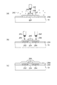
(電子装置の製造方法)
次に、図6〜図9を参照して、本発明にかかる電子装置の製造方法について説明する。図6(a)〜(d)、図7(a)〜(d)、図8(a)〜(c)、および図9(a)〜(c)は、電子装置としての薄膜トランジスタ(以下、「TFT」と称する。)の製造工程を示す模式断面図である。
(Electronic device manufacturing method)
Next, a method for manufacturing an electronic device according to the present invention will be described with reference to FIGS. FIGS. 6A to 6D, FIGS. 7A to 8D, FIGS. 8A to 8C, and FIGS. 9A to 9C are thin film transistors (hereinafter referred to as electronic devices). It is a schematic cross section showing a manufacturing process of “TFT”.
まず、図6(a)に示すように、基板10上の、TFTを形成すべき第1の領域202の周辺の領域である第2の領域204に、電子ビーム206を照射する。電子の衝撃により基板10表面の酸素原子208と結合していた水素原子、および/または基板10表面の電子が飛ばされて、ダングリングボンド210が形成される。
First, as shown in FIG. 6A, an
次に、図6(b)に示すように、基板10を所定の時間、エチルベンゼンガス212雰囲気中に静置する。上述のパターン形成方法の実施形態で述べたように、ダングリングボンド210にエチルベンゼンガスが結合して、CF3基214を形成する。CF3基214はフッ素原子により撥液性を有する。したがって、第2の領域204は、少なくとも後述するシリコン化合物の溶質を溶媒に分散した液材に対する撥液性が高められる。
Next, as shown in FIG. 6B, the
次に、図6(c)に示すように、パターンを形成すべき第1の領域202に、シリコン化合物の溶質を溶媒に分散した液材216をインクジェットヘッド218から滴下する。シリコン化合物および溶媒は上記パターン形成方法の第1の実施形態で述べたものが好ましい。
Next, as shown in FIG. 6C, a
次に、図6(d)に示すように、シリコン化合物の溶質を溶媒に分散した液材216を100℃ないし200℃に加熱することで、溶媒を乾燥除去して、シリコンの微粒子からなる薄膜パターン220を得る。
薄膜パターン220は、上述のダングリングボンド210の効果により高精細に形成可能であるが、電子ビーム206を用いてさらに形状を整えることも可能である。薄膜パターン220の周縁部に電子ビーム206を照射することで、形状を小さくする方向に調整(リファイン)可能である。
Next, as shown in FIG. 6 (d), the
The
次に、図7(a)に示すように、薄膜パターン220にレーザービーム222を照射して加熱することにより薄膜パターン220を溶融再結晶化して、チャネル層としての多結晶シリコンパターン224を得る。当該レーザー照射は、上記パターン形成方法の第1の実施形態で述べたように、酸素を含まない雰囲気中で行うことが好ましい。
Next, as shown in FIG. 7A, the
次に、基板10上全面にシリコン薄膜を形成する。まず、図7(b)に示すように、シリコンの微粒子を含有する液材228を、図示しない液材供給源に連通するノズル226から基板10の中央部に滴下する。そして基板10を回転させて均一に分布させるスピンコート法により、液材228を基板10全面に行き渡らせて、シリコンの微粒子を含有する液材228の薄膜を形成する。遠心力で液材を広げるため、基板10表面の性質の差の有無にかかわらず、ほぼ均一な厚さに液材228を分布させることができる。次に、図7(c)に示すように、基板10全体を加熱し、シリコンの微粒子を含有する液材228から溶媒を乾燥除去して、シリコン薄膜230を形成する。
Next, a silicon thin film is formed on the entire surface of the
次に、図7(d)に示すように、基板10を酸素分子232を含む雰囲気中で1000℃以上に加熱することによりシリコン薄膜230を熱酸化して、シリコン酸化膜からなるゲート絶縁膜234を形成する。なお、加熱温度はWET酸化(酸化炉に水素ガスを燃焼させて得た水蒸気を導入して酸化する手法)の場合は、ほぼ800℃で行うことができる。
Next, as shown in FIG. 7D, the silicon
次に、図8(a)に示すように、多結晶シリコンパターン224上のほぼ中央部にゲート絶縁膜234を介してタンタル等の金属原子を局所的にデポして、ゲート電極248を形成する。上記デポは収束イオンビーム(以下、「FIB」と称する。)を用いて行う。
Next, as shown in FIG. 8A, a metal electrode such as tantalum is locally deposited at a substantially central portion on the
まず、図示しない真空チャンバー内に基板10を載置して、当該チャンバー内にタンタル等の金属原子を含む反応ガス(以下、「金属ガス」と称する。)242を導入する。そして基板10上のゲート電極を形成すべき領域、すなわち上述した多結晶シリコンパターン224上のほぼ中央部に、ガリウムイオンを用いたFIB244を照射する。FIB244はニードル型の液体金属ガリウム246に電圧を印加して得る。基板10上に吸着した金属ガス242が上記照射により分解されて、タンタル等の金属原子247が堆積する。その結果、FIB244を照射した領域、すなわち多結晶シリコンパターン224上のほぼ中央部にゲート電極248が形成される。
First, the
次に、図8(b)に示すように、多結晶シリコンパターン224にリン等の不純物をイオン注入して、ソース領域252およびドレイン領域254を形成する。イオン注入もFIBにより行う。
図示するように、イオン源としてガリウムに替わるニードル型のリン250からFIB256を引出し、所定の領域にリンイオンを注入する。なお、当該工程でゲート電極248はイオン注入の際のマスクとしての機能を果たす。
Next, as shown in FIG. 8B, impurities such as phosphorus are ion-implanted into the
As shown in the figure,
次に、図8(c)に示すように基板10上全面に層間絶縁膜260を形成する。形成方法は上述したゲート絶縁膜234の形成と同様の手法による。すなわち、シリコンの微粒子を含有する液材228を基板10の中央部に滴下し(図7(b)参照)、基板10を回転させて均一に分布させた後、溶媒を乾燥除去してシリコン薄膜を得る。そして当該シリコン薄膜を酸素雰囲気中で加熱して、シリコン酸化膜からなる層間絶縁膜260を得る。
Next, an
次に、図9(a)に示すように、ソース領域252上、およびドレイン領域254上にコンタクトホール262を形成する。コンタクトホール262の形成もFIBを用いる。図示しないニードル型の液体金属ガリウム246に電圧を印加して得るFIB264を得る。そしてFIB264を基板10上の所定の領域に照射することにより層間絶縁膜260およびゲート絶縁膜234を局所的に除去して、コンタクトホール262を形成する。コンタクトホール262によりソース領域252、およびドレイン領域254の一部が露出されて、外部との導通が可能となる。
なお上記コンタクトホール262形成時に、ゲート電極248を形成するタンタル(等の金属)層の延長上にもコンタクトホールを形成することが好ましい。
Next, as shown in FIG. 9A, contact holes 262 are formed on the
Note that when the
次に、図9(b)に示すように、コンタクトホール262内にFIB278によりAl等の金属原子を堆積して、ソース電極272およびドレイン電極274を形成する。ゲート電極248の形成時と同様に、図示しない真空チャンバー内に基板10を載置して、当該チャンバー内にAl原子を含む金属ガス276を導入する。そして、コンタクトホール262内に、液体金属ガリウム246に電圧を印加して得るFIB278を照射して、Al原子277を堆積する。以上の工程により、基板10上に請求項に記載した電子装置としてのTFT(薄膜トランジスタ)290が形成される。
Next, as shown in FIG. 9B, metal atoms such as Al are deposited in the
最後に、図9(c)に示すように、ソース電極およびドレイン電極にプローブ針280を接触させる。同時に、上述するゲート電極248の延長上のコンタクトホール(図示せず)にプローブ針(図示せず)を接触させる。そしてTFT290の電気的特性を測定する。
以上の製造方法により、基板10上に電子装置としてのTFT290を形成し、電気特性の測定を行うことができる。FIBを用いて薄膜の形成あるいはパターニングを行うためフォトマスク等を用いる必要がなくなる。その結果、電子装置の試作と当該試作品の評価を低コストかつ短期間に実施できる。
Finally, as shown in FIG. 9C, the
With the above manufacturing method, the
(電子装置の製造装置)
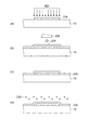
図10に、本発明の第1の実施形態かかる電子装置の製造装置の模式図を示す。本実施形態にかかる製造装置は、真空処理室402と、当該真空処理室に連通する液材供給室404と、を主体として構成されている。
(Electronic device manufacturing equipment)
FIG. 10 is a schematic diagram of an electronic device manufacturing apparatus according to the first embodiment of the present invention. The manufacturing apparatus according to the present embodiment is mainly composed of a
真空処理室402と液材供給室404との間は搬送路432で結ばれ、基板10は基板保持手段418と共に、搬送路432内を基板搬送手段としてのトランスファーロッド436で搬送される。搬送路432はゲートバルブ434で区切られ、真空処理室402と液材供給室404双方の室内の真空度等を独立して設定できる。したがって、真空処理室402内で表面の性状を変化させた基板10を、大気に晒すことなく液材供給室404に移送できる。
The
また、液材供給室404は外部と連通する基板搬入口438を備えている。ゲートバルブ434を閉じた状態で当該搬入口を開閉することで、真空処理室402内の雰囲気に影響を与えずに、当該製造装置において基板10の搬入および搬出ができる。
The liquid
真空処理室402は、エネルギービーム照射手段としてのイオン源412、電子源414および複数のガス供給源416を備え、図示しない真空ポンプと連通しており、ゲートバルブ434を閉じた状態で上記真空ポンプを作動させて内部を真空にできる。
そして、基板保持手段418で保持された基板10に、イオン源412および電子源414からFIBおよび電子ビームを照射して、当該基板10表面の性状を変化させることができる。
The
Then, the
また、真空処理室402はガス供給源416を備えているため、電子ビーム等を基板10に照射した後にガスを作用させて、基板10表面の性状を安定かつ液材の塗布に適した性状に変化させることができる。その結果、基板10上に高精細なパターンを高い再現性で形成できる。
また真空処理室402では、基板10上に薄膜を形成することもできる。ガス供給源416からガスを供給しつつFIBを照射することで、基板10上の任意の領域に薄膜を堆積させることもできる。
Further, since the
In the
液材供給室404は、駆動手段426によりX方向およびY方向に移動可能な、液材供給手段としてのインクジェットヘッド422を備えている。基板保持手段418で保持された基板10上に、インクジェットヘッド422から液材424を滴下し、溶媒を乾燥除去する工程を加えることで、当該液材に分散又は溶解している材料からなる薄膜パターンを形成できる。
The liquid
そして、液材供給室404は真空処理室402と同様に図示しない真空ポンプと連通しており、室内を大気中に比べて低圧にすることができる。また室内を満たすガス種も制御できる。したがって、真空処理室402において変化させた基板10の表面の性状が大気により変化することを抑制しつつ、インクジェットヘッド422から液材424を滴下できる。
The liquid
なお、本実施形態では基板10に液材供給手段としてインクジェットヘッド422を用いているが、基板10の中央部にのみ液材を供給するノズルを用いることも可能である。液材供給手段として上記ノズルを用いる場合、いわゆるスピンコート法により基板10全面に薄膜を形成した後、真空処理室402内で電子ビームによりパターニングすることができる。
In the present embodiment, the
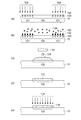
図11に本発明の第2の実施形態かかる電子装置の製造装置の模式図を示す。本実施形態にかかる製造装置は、搬送路432の両側に各々がゲートバルブ434で区切られた処理室が計8室配置されていることが特徴である。各処理室内には基板保持部500が備えられており、基板10を保持して各種の処理を施すことができる。本装置は上述するTFT290の製造方法に対応するものであり、上記処理室はそれぞれTFTの形成に必要な工程の一部を実施できる。全ての処理室を用いることで、基板10上にTFT290を形成し、さらに電気的特性の評価を行うことができる。
FIG. 11 shows a schematic diagram of an electronic device manufacturing apparatus according to a second embodiment of the present invention. The manufacturing apparatus according to the present embodiment is characterized in that a total of eight processing chambers each separated by a
各処理室はそれぞれトランスファーロッド436を備えており、搬送路432との間で基板10を行き来させることができる。そして搬送路もトランスファーロッド436を備えており、基板搬入口438から基板10を搬入又は搬出できる。各々の処理室は図示しない真空排気系と連通する排気口437を有しており、内部を任意の真空度に設定可能である。各々の処理室の機能は以下の通りである。
Each processing chamber is provided with a
第1の処理室Aは、スピンコート室である。基板保持部500を回転させる回転駆動機構502と、当該回転の中心に液材を滴下可能な、液材供給手段としての液材滴下ノズル504とを備えている。基板10を回転させつつ液材を滴下して、基板10全面に当該液材からなる薄膜を形成できる。なお、液材に含まれる溶媒(又は分散媒)を乾燥除去する工程は別途行う。
The first processing chamber A is a spin coating chamber. A
第2の処理室Bは、インクジェット室である。基板10に垂直な方向をZ方向とした場合にX方向およびY方向に移動可能な、液材供給手段としてのインクジェットヘッド512を備え、基板10上の任意の位置に機能材料を溶質とする液材514を滴下できる。第1の処理室Aと同様に、液材に含まれる溶媒等を乾燥除去する工程は別途行う。
The second processing chamber B is an ink jet chamber. A liquid having an
第3の処理室Cおよび第4の処理室Dは、真空処理室である。FIBを照射可能なイオン源522、および電子ビームを照射可能な電子源524を備えており、基板10の表面の任意の領域を照射できる。当該照射により、ダングリングボンド(図1等を参照)の形成等を実施することで、当該表面の性状を変化させることができる。
また、複数のガス供給源526を備え、ガスを供給しつつFIBを照射することで、基板10表面の任意の領域に、イオン注入、エッチング、薄膜デポ等の処理を施すことができる。
The third processing chamber C and the fourth processing chamber D are vacuum processing chambers. An
In addition, by providing a plurality of
第5の処理室Eは、焼成室である。ヒータ532により室内を加熱して、任意の温度で基板10を加熱することができ、基板10上に形成された薄膜の溶融再結晶化あるいは溶媒の乾燥除去等の処理を施すことができる。
またガス供給源526を備え、加熱中に任意のガスを供給できる。例えば酸素ガスを供給しつつ加熱して、基板上のシリコン薄膜をシリコン酸化膜とすることができ、また、窒素ガスを供給しつつ加熱してイオン注入された不純物を活性化させることもできる。
The fifth processing chamber E is a baking chamber. The interior of the
Further, a
第6の処理室Fは、レーザーアニール室である。レーザー照射源542より基板10上に形成された薄膜にレーザービームを照射して、加熱、加工、結晶化等の工程を実施できる。したがって、他の処理室を併用することで、基板上に多結晶シリコン層等を形成できる。さらに、上記シリコン層の結晶性を評価するために顕微ラマン測定装置を備えることもできる。
The sixth processing chamber F is a laser annealing chamber. By irradiating the thin film formed on the
第7の処理室Gは、SEM室である。電子源524と検出器552を備え、第1の処理室〜第6の処理室を用いて基板上に形成された構造の外観を観察できる。
The seventh processing chamber G is an SEM chamber. An
第8の処理室Hは、測定室である。外部から操作可能なプローブ針562と顕微鏡564とを備え、第1の処理室〜第6の処理室を用いて基板上に形成されたTFT等の電子装置の電極にプローブ針562を接触させることができる。プローブ針562は図示しない電気的特性評価装置に接続されており、基板10上に形成された電子装置の電気的特性を、本実施形態にかかる装置の外部から測定できる。
The eighth processing chamber H is a measurement chamber. A
以上述べたように、本実施形態の製造装置は、当該装置のみでTFT等の電子装置を形成し、電気的特性を測定できる。各工程は連続的に実施されるので、非常に短期間でTFTの製造と評価を行える。また、フォトマスクを用いずにパターンを形成するため、寸法等の修正や変更を容易に行うことができる。また、一旦装置内に搬入した基板を外部ヘ搬出することなく外観の観察等を行うことができ、その結果に基づいてさらなる処理を施すことができるので、処理条件の変更実験等を極めて短期間に実施できる。したがって、本装置を用いることでTFT等の電子装置の製造、特に試作と評価を短期間かつ低コストで実施可能となり、開発力を向上させることができる。 As described above, the manufacturing apparatus according to the present embodiment can form an electronic device such as a TFT with only the apparatus and measure the electrical characteristics. Since each process is performed continuously, it is possible to manufacture and evaluate TFTs in a very short period of time. In addition, since the pattern is formed without using a photomask, the dimensions and the like can be easily corrected and changed. In addition, it is possible to observe the appearance of the substrate once carried into the apparatus without carrying it out to the outside, and further processing can be performed based on the result. Can be implemented. Therefore, by using this apparatus, manufacturing of electronic devices such as TFTs, in particular, trial manufacture and evaluation can be performed in a short period of time and at low cost, and development capability can be improved.
10…基板、100…第1の領域、101…第2の領域、102…ダングリングボンド、104…酸素原子、106…電子ビーム、108…機能性液材、110…ノズル、112…薄膜パターン、114…レーザービーム、116…多結晶シリコン膜、120…NH3ガス、122…NH基、126…エチルベンゼンガス、128…CF3基、202…第1の領域、204…第2の領域、206…電子ビーム、208…酸素原子、210…ダングリングボンド、212…エチルベンゼンガス、214…CF3基、216…シリコン化合物の溶質を溶媒に分散した液材、218…インクジェットヘッド、220…薄膜パターン、222…レーザービーム、224…多結晶シリコンパターン、226…ノズル、228…シリコンの微粒子を含有する液材、230…シリコン薄膜、232…酸素分子、234…ゲート絶縁膜、242…金属ガス、244…FIB、246…液体金属ガリウム、247…金属原子、248…ゲート電極、250…リン、252…ソース領域、254…ドレイン領域、260…層間絶縁膜、262…コンタクトホール、264…FIB、272…ソース電極、274…ドレイン電極、276…金属ガス、277…Al原子、278…FIB、280…プローブ針、290…TFT、402…真空処理室、404…液材供給室、412…イオン源、414…電子源、416…ガス供給源、418…基板保持手段、422…インクジェットヘッド、424…液材、426…駆動手段、432…搬送路、434…ゲートバルブ、436…トランスファーロッド、437…排気口、438…基板搬入口、500…基板保持部、502…回転駆動機構、504…液材滴下ノズル、512…インクジェットヘッド、514…液材、522…イオン源、524…電子源、526…ガス供給源、532…ヒータ、542…レーザー照射源、552…検出器、562…プローブ針、564…顕微鏡、A…第1の処理室、B…第2の処理室、C…第3の処理室、D…第4の処理室、E…第5の処理室、F…第6の処理室、G…第7の処理室、H…第8の処理室。
DESCRIPTION OF
Claims (20)
第1ガス供給手段と、第2ガス排気手段と、前記基板を保持可能な第2基板保持手段と、を備え、前記第2基板保持手段で保持された前記基板上に液材を供給する液材供給手段を備える液材供給室と、
前記真空処理室と前記液材供給室との間を連絡する搬送路と、
前記搬送路を開閉する第1ゲートバルブと、
前記真空処理室と前記液材供給室との間を前記基板を搬送可能な搬送手段と、
前記真空処理室および前記液材供給室の少なくともどちらか一方に連通する基板搬入口と、
を備えることを特徴とする電子装置の製造装置。 A vacuum processing chamber including therein an energy beam irradiation unit, a first gas exhaust unit, and a first substrate holding unit capable of holding a substrate;
A liquid that includes a first gas supply unit, a second gas exhaust unit, and a second substrate holding unit capable of holding the substrate, and that supplies a liquid material onto the substrate held by the second substrate holding unit; A liquid material supply chamber comprising material supply means;
A transfer path communicating between the vacuum processing chamber and the liquid material supply chamber;
A first gate valve for opening and closing the conveyance path;
Transport means capable of transporting the substrate between the vacuum processing chamber and the liquid material supply chamber;
A substrate carry-in port communicating with at least one of the vacuum processing chamber and the liquid material supply chamber;
An apparatus for manufacturing an electronic device, comprising:
前記第1の領域に機能性材料と溶媒とを含む液材を滴下する液材滴下工程と、
を有し、
前記照射工程と前記液材滴下工程との間は、前記基板を大気に晒さずコントロールされた雰囲気中で保持することを特徴とするパターン形成方法。 An irradiation step of irradiating the first region on the substrate with an energy beam to form a dangling bond;
A liquid material dropping step of dropping a liquid material containing a functional material and a solvent in the first region;
Have
Between the irradiation process and the liquid material dropping process, the substrate is held in a controlled atmosphere without being exposed to the atmosphere.
前記ダングリングボンドと結合して当該結合により親液性表面を形成する性質を有するガスを供給することにより、機能性材料と溶媒とを含む液材に対する前記第1の領域の親液性を高めるガス処理工程と、
前記第1の領域に前記液材を滴下する滴下工程と、
を含み、
前記照射工程と前記ガス処理工程との間、および前記ガス処理工程と前記滴下工程との間は、前記基板を大気に晒さずコントロールされた雰囲気中で保持することを特徴とするパターン形成方法。 An irradiation step of irradiating the first region on the substrate with an energy beam to form a dangling bond;
By supplying a gas having a property of forming a lyophilic surface by bonding with the dangling bond, the lyophilicity of the first region with respect to a liquid material containing a functional material and a solvent is increased. A gas treatment process;
A dropping step of dropping the liquid material into the first region;
Including
The pattern forming method, wherein the substrate is held in a controlled atmosphere without being exposed to the atmosphere between the irradiation step and the gas treatment step, and between the gas treatment step and the dropping step.
前記ダングリングボンドと結合して当該結合により撥液性表面を形成する性質を有するガスを供給することにより、機能性材料と溶媒とを含む液材に対する前記第2の領域の撥液性を高めるガス処理工程と、
前記第1の領域に前記液材を滴下する滴下工程と、
を含み、
前記照射工程と前記ガス処理工程との間、および前記ガス処理工程と前記滴下工程との間は、前記基板を大気に晒さずコントロールされた雰囲気中で保持することを特徴とするパターン形成方法。 An irradiation step of irradiating an energy beam to a second region, which is a region other than the first region, on the substrate to form a dangling bond;
By supplying a gas having a property of forming a liquid-repellent surface by bonding with the dangling bond, the liquid repellency of the second region with respect to a liquid material containing a functional material and a solvent is increased. A gas treatment process;
A dropping step of dropping the liquid material into the first region;
Including
The pattern forming method, wherein the substrate is held in a controlled atmosphere without being exposed to the atmosphere between the irradiation step and the gas treatment step, and between the gas treatment step and the dropping step.
前記第1の領域に機能性材料と溶媒とを含む液材を滴下した後に前記溶媒を除去して、前記機能性材料を含む薄膜を形成する薄膜形成工程と、
を有し、
前記照射工程と前記薄膜形成工程との間は、前記基板を大気に晒さずコントロールされた雰囲気中で保持することを特徴とする電子装置の製造方法。 An irradiation step of irradiating the first region on the substrate with an energy beam to form a dangling bond;
A thin film forming step of forming a thin film containing the functional material by dropping the solvent after dropping a liquid material containing the functional material and the solvent in the first region;
Have
Between the irradiation process and the thin film formation process, the substrate is held in a controlled atmosphere without being exposed to the atmosphere.
前記ダングリングボンドと結合して、当該結合により親液性表面を形成する性質を有するガスを供給することにより、機能性材料と溶媒とを含む液材に対する前記第1の領域の親液性を高めるガス処理工程と、
前記第1の領域に前記液材を滴下した後に前記溶媒を除去して、前記機能性材料を含む薄膜を形成する薄膜形成工程と、
を有し、
前記照射工程と前記ガス処理工程との間、および前記ガス処理工程と前記薄膜形成工程との間は、前記基板を大気に晒さずコントロールされた雰囲気中で保持することを特徴とする電子装置の製造方法。 An irradiation step of irradiating the first region on the substrate with an energy beam to form a dangling bond;
By combining with the dangling bond and supplying a gas having a property of forming a lyophilic surface by the bonding, the lyophilicity of the first region with respect to a liquid material containing a functional material and a solvent is increased. Enhanced gas treatment process;
A thin film forming step of forming the thin film containing the functional material by removing the solvent after dropping the liquid material in the first region;
Have
An electronic device characterized in that the substrate is held in a controlled atmosphere without being exposed to the atmosphere between the irradiation step and the gas treatment step and between the gas treatment step and the thin film formation step. Production method.
前記基板を形成する材料とは反応せず、前記ダングリングボンドとは結合して表面を撥液性にする性質を有するガスを供給して、機能性材料と溶媒とを含む液材に対する前記第2の領域の撥液性を高めるガス処理工程と、
前記ダングリングボンドと結合して、当該結合により撥液性表面を形成する性質を有するガスを供給することにより、前記液材に対する前記第2の領域の撥液性を高めるガス処理工程と、
前記第1の領域に前記液材を滴下した後に前記溶媒を除去して、前記機能性材料を含む薄膜を形成する薄膜形成工程と、
を有し、
前記照射工程と前記ガス処理工程との間、および前記ガス処理工程と前記薄膜形成工程との間は、前記基板を大気に晒さずコントロールされた雰囲気中で保持することを特徴とする電子装置の製造方法。 An irradiation step of irradiating an energy beam to a second region, which is a region other than the first region, on the substrate to form a dangling bond;
The gas for the liquid material containing the functional material and the solvent is supplied by supplying a gas that does not react with the material forming the substrate and is bonded to the dangling bond to make the surface liquid-repellent. A gas treatment step for increasing the liquid repellency of the region 2;
A gas treatment step of increasing the liquid repellency of the second region with respect to the liquid material by supplying a gas having a property of forming a liquid repellent surface by the bonding with the dangling bond;
A thin film forming step of forming the thin film containing the functional material by removing the solvent after dropping the liquid material in the first region;
Have
An electronic device characterized in that the substrate is held in a controlled atmosphere without being exposed to the atmosphere between the irradiation step and the gas treatment step and between the gas treatment step and the thin film formation step. Production method.
前記コンタクトホール内に導電性物質を充填してソース電極およびドレイン電極を形成する工程と、
をさらに含むことを特徴とする請求項19に記載の電子装置の製造方法。 Removing a part of the interlayer insulating film locally using a focused ion beam and forming a contact hole in a region not overlapping the gate electrode on the channel layer;
Filling the contact hole with a conductive material to form a source electrode and a drain electrode;
The method of manufacturing an electronic device according to claim 19, further comprising:
Priority Applications (1)
| Application Number | Priority Date | Filing Date | Title |
|---|---|---|---|
| JP2007033111A JP2008198822A (en) | 2007-02-14 | 2007-02-14 | Pattern formation method, electronic device manufacturing method, and electronic device manufacturing apparatus |
Applications Claiming Priority (1)
| Application Number | Priority Date | Filing Date | Title |
|---|---|---|---|
| JP2007033111A JP2008198822A (en) | 2007-02-14 | 2007-02-14 | Pattern formation method, electronic device manufacturing method, and electronic device manufacturing apparatus |
Publications (1)
| Publication Number | Publication Date |
|---|---|
| JP2008198822A true JP2008198822A (en) | 2008-08-28 |
Family
ID=39757501
Family Applications (1)
| Application Number | Title | Priority Date | Filing Date |
|---|---|---|---|
| JP2007033111A Withdrawn JP2008198822A (en) | 2007-02-14 | 2007-02-14 | Pattern formation method, electronic device manufacturing method, and electronic device manufacturing apparatus |
Country Status (1)
| Country | Link |
|---|---|
| JP (1) | JP2008198822A (en) |
Cited By (3)
| Publication number | Priority date | Publication date | Assignee | Title |
|---|---|---|---|---|
| JP2014175502A (en) * | 2013-03-08 | 2014-09-22 | Nippon Hoso Kyokai <Nhk> | Manufacturing method of thin film transistor element and patterning method of printable semiconductor layer |
| JP2018165644A (en) * | 2017-03-28 | 2018-10-25 | セイコーエプソン株式会社 | Method for adjusting frequency of vibration element, method for manufacturing vibration element, and vibration element |
| WO2025068618A3 (en) * | 2023-09-29 | 2025-05-22 | Consejo Superior De Investigaciones Científicas (Csic) | System for manufacturing electrical contacts and associated manufacturing method |
-
2007
- 2007-02-14 JP JP2007033111A patent/JP2008198822A/en not_active Withdrawn
Cited By (3)
| Publication number | Priority date | Publication date | Assignee | Title |
|---|---|---|---|---|
| JP2014175502A (en) * | 2013-03-08 | 2014-09-22 | Nippon Hoso Kyokai <Nhk> | Manufacturing method of thin film transistor element and patterning method of printable semiconductor layer |
| JP2018165644A (en) * | 2017-03-28 | 2018-10-25 | セイコーエプソン株式会社 | Method for adjusting frequency of vibration element, method for manufacturing vibration element, and vibration element |
| WO2025068618A3 (en) * | 2023-09-29 | 2025-05-22 | Consejo Superior De Investigaciones Científicas (Csic) | System for manufacturing electrical contacts and associated manufacturing method |
Similar Documents
| Publication | Publication Date | Title |
|---|---|---|
| JP4922335B2 (en) | Substrate processing equipment | |
| TWI408247B (en) | Method for forming metal oxide film and film forming device | |
| US20050089635A1 (en) | Pattern forming method, conductive thin film, electro-optic device, and electronic equipment | |
| CN101689501A (en) | Method for manufacturing semiconductor device, semiconductor manufacturing apparatus, and storage medium | |
| JP2001179167A (en) | Thin film deposition method | |
| US20030087110A1 (en) | Method for fabricating a silicon thin-film | |
| TW200301939A (en) | Method of treating substrate and method of manufacturing semiconductor device | |
| JP2020524402A (en) | Selective deposition process using polymer structure deactivation process | |
| KR101285450B1 (en) | Method for high resolution processing of thin layers using electron beams | |
| JP2008198822A (en) | Pattern formation method, electronic device manufacturing method, and electronic device manufacturing apparatus | |
| Park et al. | A self-aligned high resolution patterning process for large area printed electronics | |
| TWI399810B (en) | Inorganic semiconductor film and method of manufacturing same | |
| CN107851558B (en) | UV-assisted injection of materials into porous membranes | |
| JP6386394B2 (en) | Compound process equipment | |
| JP3859744B2 (en) | Method for manufacturing semiconductor device and active matrix display device | |
| US20080009143A1 (en) | Method of forming silicon oxide layer | |
| JP7416988B1 (en) | Substrate processing equipment and substrate processing method | |
| US12240752B2 (en) | Method for producing a sequencing unit for sequencing a biochemical material and sequencing unit | |
| JP2010116303A (en) | Substrate for growing carbon nanotube, transistor, and method for manufacturing substrate for growing carbon nanotube | |
| KR102388445B1 (en) | Improved Apparatus and Method for Manufacturing Oxide Thin Film Using Low-Temperature Process | |
| JPH06110197A (en) | Method and apparatus for forming a fine pattern mask | |
| JP2005123355A (en) | Method for forming polysilicon film and thin film transistor comprising polysilicon film formed by the method | |
| TWI875058B (en) | Semiconductor device and method of manufacturing thereof | |
| JP2008028405A (en) | Semiconductor thin-film reforming apparatus | |
| JP2007142451A (en) | Insulating layer, insulating layer pattern, thin film transistor, liquid crystal display, and liquid pattern formation device |
Legal Events
| Date | Code | Title | Description |
|---|---|---|---|
| A300 | Withdrawal of application because of no request for examination |
Free format text: JAPANESE INTERMEDIATE CODE: A300 Effective date: 20100511 |