JP2008166318A - Photo sensor - Google Patents
Photo sensor Download PDFInfo
- Publication number
- JP2008166318A JP2008166318A JP2006350769A JP2006350769A JP2008166318A JP 2008166318 A JP2008166318 A JP 2008166318A JP 2006350769 A JP2006350769 A JP 2006350769A JP 2006350769 A JP2006350769 A JP 2006350769A JP 2008166318 A JP2008166318 A JP 2008166318A
- Authority
- JP
- Japan
- Prior art keywords
- photoelectric conversion
- thin film
- drain electrode
- semiconductor thin
- source electrode
- Prior art date
- Legal status (The legal status is an assumption and is not a legal conclusion. Google has not performed a legal analysis and makes no representation as to the accuracy of the status listed.)
- Granted
Links
Images

Classifications
-
- H—ELECTRICITY
- H10—SEMICONDUCTOR DEVICES; ELECTRIC SOLID-STATE DEVICES NOT OTHERWISE PROVIDED FOR
- H10F—INORGANIC SEMICONDUCTOR DEVICES SENSITIVE TO INFRARED RADIATION, LIGHT, ELECTROMAGNETIC RADIATION OF SHORTER WAVELENGTH OR CORPUSCULAR RADIATION
- H10F77/00—Constructional details of devices covered by this subclass
- H10F77/20—Electrodes
- H10F77/206—Electrodes for devices having potential barriers
-
- H—ELECTRICITY
- H10—SEMICONDUCTOR DEVICES; ELECTRIC SOLID-STATE DEVICES NOT OTHERWISE PROVIDED FOR
- H10D—INORGANIC ELECTRIC SEMICONDUCTOR DEVICES
- H10D64/00—Electrodes of devices having potential barriers
- H10D64/20—Electrodes characterised by their shapes, relative sizes or dispositions
- H10D64/23—Electrodes carrying the current to be rectified, amplified, oscillated or switched, e.g. sources, drains, anodes or cathodes
-
- H—ELECTRICITY
- H10—SEMICONDUCTOR DEVICES; ELECTRIC SOLID-STATE DEVICES NOT OTHERWISE PROVIDED FOR
- H10F—INORGANIC SEMICONDUCTOR DEVICES SENSITIVE TO INFRARED RADIATION, LIGHT, ELECTROMAGNETIC RADIATION OF SHORTER WAVELENGTH OR CORPUSCULAR RADIATION
- H10F30/00—Individual radiation-sensitive semiconductor devices in which radiation controls the flow of current through the devices, e.g. photodetectors
- H10F30/20—Individual radiation-sensitive semiconductor devices in which radiation controls the flow of current through the devices, e.g. photodetectors the devices having potential barriers, e.g. phototransistors
- H10F30/21—Individual radiation-sensitive semiconductor devices in which radiation controls the flow of current through the devices, e.g. photodetectors the devices having potential barriers, e.g. phototransistors the devices being sensitive to infrared, visible or ultraviolet radiation
- H10F30/28—Individual radiation-sensitive semiconductor devices in which radiation controls the flow of current through the devices, e.g. photodetectors the devices having potential barriers, e.g. phototransistors the devices being sensitive to infrared, visible or ultraviolet radiation the devices being characterised by field-effect operation, e.g. junction field-effect phototransistors
- H10F30/282—Insulated-gate field-effect transistors [IGFET], e.g. MISFET [metal-insulator-semiconductor field-effect transistor] phototransistors
-
- H—ELECTRICITY
- H10—SEMICONDUCTOR DEVICES; ELECTRIC SOLID-STATE DEVICES NOT OTHERWISE PROVIDED FOR
- H10F—INORGANIC SEMICONDUCTOR DEVICES SENSITIVE TO INFRARED RADIATION, LIGHT, ELECTROMAGNETIC RADIATION OF SHORTER WAVELENGTH OR CORPUSCULAR RADIATION
- H10F30/00—Individual radiation-sensitive semiconductor devices in which radiation controls the flow of current through the devices, e.g. photodetectors
- H10F30/20—Individual radiation-sensitive semiconductor devices in which radiation controls the flow of current through the devices, e.g. photodetectors the devices having potential barriers, e.g. phototransistors
- H10F30/21—Individual radiation-sensitive semiconductor devices in which radiation controls the flow of current through the devices, e.g. photodetectors the devices having potential barriers, e.g. phototransistors the devices being sensitive to infrared, visible or ultraviolet radiation
- H10F30/28—Individual radiation-sensitive semiconductor devices in which radiation controls the flow of current through the devices, e.g. photodetectors the devices having potential barriers, e.g. phototransistors the devices being sensitive to infrared, visible or ultraviolet radiation the devices being characterised by field-effect operation, e.g. junction field-effect phototransistors
- H10F30/2823—Individual radiation-sensitive semiconductor devices in which radiation controls the flow of current through the devices, e.g. photodetectors the devices having potential barriers, e.g. phototransistors the devices being sensitive to infrared, visible or ultraviolet radiation the devices being characterised by field-effect operation, e.g. junction field-effect phototransistors the devices being conductor-insulator-semiconductor devices, e.g. diodes or charge-coupled devices [CCD]
-
- H—ELECTRICITY
- H10—SEMICONDUCTOR DEVICES; ELECTRIC SOLID-STATE DEVICES NOT OTHERWISE PROVIDED FOR
- H10F—INORGANIC SEMICONDUCTOR DEVICES SENSITIVE TO INFRARED RADIATION, LIGHT, ELECTROMAGNETIC RADIATION OF SHORTER WAVELENGTH OR CORPUSCULAR RADIATION
- H10F77/00—Constructional details of devices covered by this subclass
- H10F77/10—Semiconductor bodies
- H10F77/16—Material structures, e.g. crystalline structures, film structures or crystal plane orientations
- H10F77/169—Thin semiconductor films on metallic or insulating substrates
- H10F77/1692—Thin semiconductor films on metallic or insulating substrates the films including only Group IV materials
-
- H—ELECTRICITY
- H10—SEMICONDUCTOR DEVICES; ELECTRIC SOLID-STATE DEVICES NOT OTHERWISE PROVIDED FOR
- H10F—INORGANIC SEMICONDUCTOR DEVICES SENSITIVE TO INFRARED RADIATION, LIGHT, ELECTROMAGNETIC RADIATION OF SHORTER WAVELENGTH OR CORPUSCULAR RADIATION
- H10F39/00—Integrated devices, or assemblies of multiple devices, comprising at least one element covered by group H10F30/00, e.g. radiation detectors comprising photodiode arrays
- H10F39/10—Integrated devices
- H10F39/12—Image sensors
- H10F39/198—Contact-type image sensors [CIS]
-
- Y—GENERAL TAGGING OF NEW TECHNOLOGICAL DEVELOPMENTS; GENERAL TAGGING OF CROSS-SECTIONAL TECHNOLOGIES SPANNING OVER SEVERAL SECTIONS OF THE IPC; TECHNICAL SUBJECTS COVERED BY FORMER USPC CROSS-REFERENCE ART COLLECTIONS [XRACs] AND DIGESTS
- Y02—TECHNOLOGIES OR APPLICATIONS FOR MITIGATION OR ADAPTATION AGAINST CLIMATE CHANGE
- Y02E—REDUCTION OF GREENHOUSE GAS [GHG] EMISSIONS, RELATED TO ENERGY GENERATION, TRANSMISSION OR DISTRIBUTION
- Y02E10/00—Energy generation through renewable energy sources
- Y02E10/50—Photovoltaic [PV] energy
Landscapes
- Solid State Image Pick-Up Elements (AREA)
- Light Receiving Elements (AREA)
- Thin Film Transistor (AREA)
Abstract
【課題】 光電変換半導体薄膜上の両側に遮光性導電材料からなるソース電極およびドレイン電極が設けられたフォトセンサにおいて、光電変換半導体薄膜への光入射量を多くする。
【解決手段】 クロム等の遮光性導電材料からなるソース電極9およびドレイン電極10の相対向する側には切欠部9c、10cが設けられている。これらの切欠部9c、10cは光透過部となるので、光電変換半導体薄膜5への真上からの光入射量のみならず斜め方向からの光入射量をも多くすることができる。
【選択図】 図1PROBLEM TO BE SOLVED: To increase the amount of light incident on a photoelectric conversion semiconductor thin film in a photosensor provided with a source electrode and a drain electrode made of a light-shielding conductive material on both sides on the photoelectric conversion semiconductor thin film.
Notches 9c and 10c are provided on opposite sides of a source electrode 9 and a drain electrode 10 made of a light-shielding conductive material such as chromium. Since these notches 9c and 10c become light transmitting portions, not only the amount of light incident on the photoelectric conversion semiconductor thin film 5 but also the amount of light incident from an oblique direction can be increased.
[Selection] Figure 1
Description
この発明はフォトセンサに関する。 The present invention relates to a photosensor.
従来のフォトセンサには、アモルファスシリコンからなる光電変換半導体薄膜下にボトムゲート絶縁膜を介して遮光性導電材料からなるボトムゲート電極が設けられ、光電変換半導体薄膜上にトップゲート絶縁膜を介して透光性導電材料からなるトップゲート電極が設けられ、トップゲート絶縁膜下における光電変換半導体薄膜の上面両側にn型アモルファスシリコンからなる一対のオーミックコンタクト層を介して遮光性導電材料からなるソース電極およびドレイン電極が設けられたものがある(例えば、特許文献1参照)。この場合、ソース電極およびドレイン電極の相対向する端面は平行し、その間の間隔がチャネル長となっている。 A conventional photosensor is provided with a bottom gate electrode made of a light-shielding conductive material via a bottom gate insulating film under a photoelectric conversion semiconductor thin film made of amorphous silicon, and via a top gate insulating film on the photoelectric conversion semiconductor thin film. A source electrode made of a light-shielding conductive material is provided with a top gate electrode made of a light-transmitting conductive material and a pair of ohmic contact layers made of n-type amorphous silicon on both sides of the upper surface of the photoelectric conversion semiconductor thin film under the top gate insulating film And a drain electrode (see, for example, Patent Document 1). In this case, the opposing end surfaces of the source electrode and the drain electrode are parallel to each other, and the interval therebetween is the channel length.
しかしながら、上記従来のフォトセンサでは、光電変換半導体薄膜の上面両側に一対のオーミックコンタクト層を介して遮光性導電材料からなるソース電極およびドレイン電極が設けられ、ソース電極およびドレイン電極の相対向する端面が平行しているので、ソース電極およびドレイン電極の相対向する平行な端部が光電変換半導体薄膜への、特に、斜め方向からの光入射を遮り、十分な光感度(明電流/暗電流)を確保することができないという問題があった。 However, in the conventional photosensor, a source electrode and a drain electrode made of a light-shielding conductive material are provided on both sides of the upper surface of the photoelectric conversion semiconductor thin film via a pair of ohmic contact layers, and opposite end surfaces of the source electrode and the drain electrode are opposed to each other. Since the parallel edges of the source and drain electrodes are parallel to each other, the light incident on the photoelectric conversion semiconductor thin film, particularly from an oblique direction, is blocked, and sufficient photosensitivity (bright current / dark current) is obtained. There was a problem that could not be secured.
そこで、この発明は、光電変換半導体薄膜への光入射量を多くすることができるフォトセンサを提供することを目的とする。 Accordingly, an object of the present invention is to provide a photosensor capable of increasing the amount of light incident on the photoelectric conversion semiconductor thin film.
請求項1に記載の発明は、光電変換半導体薄膜の上面両側に一対のオーミックコンタクト層を介して遮光性導電材料からなるソース電極およびドレイン電極が設けられたフォトセンサにおいて、前記ソース電極および前記ドレイン電極の相対向する側に切欠部が設けられていることを特徴とするものである。
請求項2に記載の発明は、請求項1に記載の発明において、前記一対のオーミックコンタクト層は、前記光電変換半導体薄膜の上面中央部に設けられたチャネル保護膜の上面両側およびその両側における前記光電変換半導体薄膜の上面に設けられていることを特徴とするものである。
請求項3に記載の発明は、請求項1に記載の発明において、前記ソース電極および前記ドレイン電極の切欠部は複数で等間隔に設けられていることを特徴とするものである。
請求項4に記載の発明は、請求項1〜3のいずれかに記載の発明において、前記ソース電極および前記ドレイン電極の切欠部のチャネル幅方向の寸法はチャネル長以下であることを特徴とするものである。
請求項5に記載の発明は、請求項1〜3のいずれかに記載の発明において、前記ソース電極および前記ドレイン電極の切欠部のチャネル幅方向の寸法は前記ソース電極の切欠部以外の部分と前記ドレイン電極の切欠部以外の部分との間の間隔と同じであることを特徴とするものである。
請求項6に記載の発明は、請求項1〜3のいずれかに記載の発明において、前記ソース電極および前記ドレイン電極の切欠部に対応する部分における前記一対のオーミックコンタクト層および前記光電変換半導体薄膜に切欠部が設けられていることを特徴とするものである。
請求項7に記載の発明は、請求項1〜3のいずれかに記載の発明において、前記ソース電極および前記ドレイン電極の切欠部に対応する部分に前記一対のオーミックコンタクト層および前記光電変換半導体薄膜が設けられていることを特徴とするものである。
請求項8に記載の発明は、請求項6または7に記載の発明において、前記ソース電極および前記ドレイン電極の相対向する側とは反対側の端面は前記光電変換半導体薄膜の同方向の両端面の外側に配置されていることを特徴とするものである。
請求項9に記載の発明は、請求項6または7に記載の発明において、前記一対のオーミックコンタクト層および前記光電変換半導体薄膜は前記ソース電極および前記ドレイン電極下の全体に設けられていることを特徴とするものである。
The invention according to
According to a second aspect of the present invention, in the first aspect of the invention, the pair of ohmic contact layers includes the channel protection film provided at a center portion of the upper surface of the photoelectric conversion semiconductor thin film on both sides of the upper surface and both sides thereof. It is provided on the upper surface of the photoelectric conversion semiconductor thin film.
According to a third aspect of the present invention, in the first aspect of the present invention, a plurality of cutout portions of the source electrode and the drain electrode are provided at equal intervals.
According to a fourth aspect of the present invention, in the invention according to any one of the first to third aspects, the dimension in the channel width direction of the notch portions of the source electrode and the drain electrode is equal to or less than the channel length. Is.
According to a fifth aspect of the present invention, in the invention according to any one of the first to third aspects, the dimension in the channel width direction of the notch portions of the source electrode and the drain electrode is a portion other than the notch portion of the source electrode. The distance between the drain electrode and the portion other than the notch is the same.
The invention according to
The invention according to
The invention according to
The invention according to
この発明によれば、遮光性導電材料からなるソース電極およびドレイン電極の相対向する側に切欠部を設けているので、当該切欠部が光透過部となり、光電変換半導体薄膜への真上からの光入射量のみならず斜め方向からの光入射量をも多くすることができる。 According to the present invention, since the notch portions are provided on the opposite sides of the source electrode and the drain electrode made of the light-shielding conductive material, the notch portions serve as the light transmission portions, and are directly above the photoelectric conversion semiconductor thin film. Not only the amount of light incident but also the amount of light incident from an oblique direction can be increased.
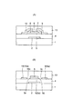
(第1実施形態)
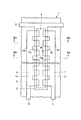
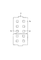
図1はこの発明の第1実施形態としてのフォトセンサの透過平面図を示し、図2(A)は図1のIIA−IIA線に沿う断面図を示し、図2(B)は図1のIIB−IIB線に沿う断面図を示す。このフォトセンサはガラス等からなる基板1を備えている。基板1の上面にはクロム等からなる帯状のゲート電極2および該ゲート電極2に接続されたゲートライン3が設けられている。
(First embodiment)
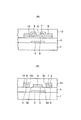
FIG. 1 is a transmission plan view of a photosensor as a first embodiment of the present invention, FIG. 2 (A) is a sectional view taken along line II A -II A in FIG. 1, and FIG. It shows a cross-sectional view taken along the first II B -II B line. This photosensor includes a
ゲート電極2およびゲートライン3を含む基板1の上面には窒化シリコン等からなるゲート絶縁膜4が設けられている。ゲート電極2上におけるゲート絶縁膜4の上面には真性アモルファスシリコンからなる光電変換半導体薄膜5が設けられている。光電変換半導体薄膜5の平面形状については後で説明する。
A gate
光電変換半導体薄膜5の上面のチャネル長L方向の中央部には窒化シリコン等からなる帯状のチャネル保護膜6が設けられている。チャネル保護膜6の上面のチャネル長L方向の両側およびその両側における光電変換半導体薄膜5の上面にはn型アモルファスシリコンからなるオーミックコンタクト層7、8が設けられている。オーミックコンタクト層7、8の平面形状については後で説明する。
A band-shaped channel
オーミックコンタクト層7、8の各上面およびその各近傍のゲート絶縁膜4の上面にはクロム等からなるソース電極9およびドレイン電極10が設けられている。ソース電極9およびドレイン電極10の平面形状については後で説明する。ゲート絶縁膜4の上面の各所定の箇所にはクロム等からなるソースライン11およびドレインライン12がソース電極9およびドレイン電極10に接続されてが設けられている。チャネル保護膜6、ソース電極9、ドレイン電極10、ソースライン11およびドレインライン12を含むゲート絶縁膜4の上面には窒化シリコン等からなるオーバーコート膜13が設けられている。
A
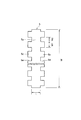
次に、ソース電極9およびドレイン電極10の平面形状について説明する。図1に示すように、ソース電極9およびドレイン電極10は、帯状部9a、10aの相対向する側に複数の方形状の突出部9b、10bが等間隔に設けられ、突出部9b、9b間および突出部10b、10b間に方形状の切欠部9c、10cが設けられた構造となっている。
Next, the planar shapes of the
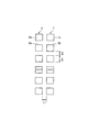
次に、光電変換半導体薄膜5の平面形状について説明する。光電変換半導体薄膜5は、図3に示すように、図1に示す帯状のチャネル保護膜6下に設けられた帯状部5a(図2(B)参照)のチャネル長L方向両側に複数の方形状の突出部5b、5cが等間隔に設けられ、突出部5b、5b間および突出部5c、5cに方形状の切欠部5d、5eが設けられた構造となっている。
Next, the planar shape of the photoelectric conversion semiconductor
この場合、切欠部5d、5eは、図1に示すソース電極9およびドレイン電極10の切欠部9c、10cと対応する位置に設けられている。突出部5b、5cは、図1に示すソース電極9およびドレイン電極10の突出部9b、10cと対応する位置に設けられている。
In this case, the
また、切欠部5d、5eの部分における光電変換半導体薄膜5の両端面は、図1に示すチャネル保護膜6のチャネル長L方向の両端面と同一の位置となっている(図2(B)参照)。突出部5b、5cの部分における光電変換半導体薄膜5のチャネル長L方向の右端面および左端面は、図1に示す切欠部9c、10cの部分におけるソース電極9の左端面およびドレイン電極10の右端面と同一の位置となっている。したがって、ソース電極9およびドレイン電極10の相対向する側とは反対側の端面は光電変換半導体薄膜5の同方向の両端面の外側に配置されている。
Further, both end faces of the photoelectric conversion semiconductor
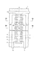
次に、オーミックコンタクト層7、8の平面形状について説明する。オーミックコンタクト層7、8は、図4に示すように、複数の方形状部7a、8aがチャネル幅W方向に等間隔に設けられ、方形状部7a、7a間および方形状部8a、8aに方形状の切欠部7b、8bが設けられた構造となっている。
Next, the planar shape of the
この場合、切欠部7b、8bは、図1に示すソース電極9およびドレイン電極10の切欠部9c、10cと同一の位置に設けられている。方形状部7a、8aは、図1に示すソース電極9およびドレイン電極10の突出部9b、10b下にのみ設けられている。
In this case, the
以上のように、このフォトセンサでは、クロム等の遮光性導電材料からなるソース電極9およびドレイン電極10の相対向する側に切欠部9c、10cを設け、これと同じ箇所におけるオーミックコンタクト層7、8および光電変換半導体薄膜5に切欠部7b、8bおよび切欠部5d、5eを設けているので、これらの切欠部が光透過部となり、光電変換半導体薄膜5への真上からの光入射量のみならず斜め方向からの光入射量をも多くすることができる。
As described above, in this photosensor, the
ところで、図2(B)に示すように、ソース電極9およびドレイン電極10は、切欠部5d、(7b)、9cおよび切欠部5e、(8b)、10cに対応する部分において、光電変換半導体薄膜5に接続されていない。しかるに、突出部9b、10bの部分におけるソース電極9、ドレイン電極10およびその下に設けられたオーミックコンタクト層7、8のフリンジ効果(チャネルの端部効果)により電流が回り込んで流れるため、切欠部5d、5eの部分における光電変換半導体薄膜5にも十分な光電流を流すことができる。
By the way, as shown in FIG. 2B, the
ただし、切欠部5d、7b、9cおよび切欠部5e、8b、10cのチャネル幅W方向の寸法W2が大きくなると、フリンジ効果で流れる電流が減少するため、光電変換半導体薄膜5の切欠部の幅W2はチャネル長L以下である方が好ましい。通常、図1におけるソース電極9とドレイン電極10のチャネル長方向の間隔L1は、ソース電極9とドレイン電極10をパターニングする際のエッチング加工が可能な最小寸法程度にする。
However, when the dimension W2 in the channel width W direction of the
光電変換半導体薄膜5の切欠部のチャネル幅方向の寸法W2も、上述のフリンジ効果を十分に得るためには、限定する訳ではないが、やはり、光電変換半導体薄膜5をパターニングする際のエッチング加工が可能な最小寸法程度とすることが望ましい。従って、光電変換半導体薄膜5の切欠部のチャネル幅方向の寸法W2と、ソース電極9とドレイン電極10のチャネル長方向の間隔L1は、共に最小加工寸法となり、換言すれば、同一寸法となる。
The dimension W2 in the channel width direction of the cutout portion of the photoelectric conversion semiconductor
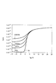
次に、実験例について説明する。まず、フォトセンサとして、図1〜図4に示すように、チャネル幅Wが20000μmであり、ソース電極9およびドレイン電極10の突出部9b、10bのチャネル幅W方向の寸法W1が6μmであり、切欠部5d、5eのチャネル幅方向の寸法W2が4μmであり、チャネル長Lが9μmであり、間隔L1が4μmであるものを用意した(以下、本発明品という)。
Next, experimental examples will be described. First, as a photosensor, as shown in FIGS. 1 to 4, the channel width W is 20000 μm, the dimension W1 in the channel width W direction of the protruding
また、比較のために、図1〜図4に示すフォトセンサを参照して説明すると、光電変換半導体薄膜5、オーミックコンタクト層7、8、ソース電極9およびドレイン電極10に切欠部5d、5e、7b、8b、9c、10cが形成されていないものを用意した(以下、比較品という)。
For comparison, the photo sensor shown in FIGS. 1 to 4 will be described. The photoelectric conversion semiconductor
すなわち、この比較品においては、ソース電極及びドレイン電極は、図1を参照して説明すると、チャネル長L方向の寸法が突出部9b、10bの部分におけるソース電極9およびドレイン電極10の同方向の寸法と同じである単なる帯状のものからなっている。光電変換半導体薄膜は、図3を参照して説明すると、チャネル長L方向の寸法が突出部5b、5cの部分における光電変換半導体薄膜5の同方向の寸法と同じである単なる帯状のものからなっている。一対のオーミックコンタクト層は、図4を参照して説明すると、チャネル長L方向の寸法が方形状部7a、8aの同方向の寸法と同じである単なる帯状のものからなっている。
In other words, in this comparative product, the source electrode and the drain electrode are described with reference to FIG. 1, and the dimension in the channel length L direction is the same as that of the
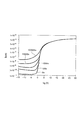
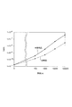
さて、本発明品および比較品について、ソース電圧0V、ドレイン電圧10Vとして、光強度(照度、0lx、100lx、1000lx、10000lx、100000lx)に対するVg−Id特性を調べたところ、図5(本発明品)および図6(比較品)に示す結果が得られた。そして、図5および図6に基づいて、ソース電圧0V、ドレイン電圧10V、ゲート電圧マイナス10Vとして、光強度(照度)に対するオフ電流を求めたところ、図7に示す結果が得られた。図7において、実線は本発明品であり、点線は比較品である。 When the Vg-Id characteristics with respect to the light intensity (illuminance, 0 lx, 100 lx, 1000 lx, 10000 lx, 100000 lx) were examined for the product of the present invention and the comparative product at a source voltage of 0 V and a drain voltage of 10 V, FIG. ) And the results shown in FIG. 6 (comparative product) were obtained. Then, based on FIG. 5 and FIG. 6, when the off-current with respect to the light intensity (illuminance) was obtained with the source voltage 0 V, the drain voltage 10 V, and the gate voltage minus 10 V, the result shown in FIG. 7 was obtained. In FIG. 7, the solid line is the product of the present invention, and the dotted line is the comparative product.
図7から明らかなように、実線で示す本発明品では、暗電流(0lx)の値が点線で示す比較品とほとんど同じであるが、明電流(100〜10000lx)の値が点線で示す比較品と比較して約1桁増大している。したがって、本発明品では、比較品と比較して光感度(明電流/暗電流)が約1桁向上していると言える。 As is clear from FIG. 7, the dark current (Olx) value of the present invention product indicated by the solid line is almost the same as the comparative product indicated by the dotted line, but the bright current (100 to 10000 lx) value is indicated by the dotted line. Compared to products, it has increased by an order of magnitude. Therefore, it can be said that the photosensitivity (bright current / dark current) of the product of the present invention is improved by about one digit compared to the comparative product.
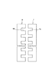
(第2実施形態)
図8はこの発明の第2実施形態としてのフォトセンサの透過平面図を示し、図9(A)は図8のIXA−IXA線に沿う断面図を示し、図9(B)は図8のIXB−IXB線に沿う断面図を示し、図10は図8および図9に示す光電変換半導体薄膜の平面図を示し、図11は図8および図9に示すオーミックコンタクト層の平面図を示す。
(Second Embodiment)
8 shows a transmission plan view of a photosensor as a second embodiment of the present invention, FIG. 9A shows a cross-sectional view taken along line IX A -IX A in FIG. 8, and FIG. 8 is a sectional view taken along line IX B -IX B , FIG. 10 is a plan view of the photoelectric conversion semiconductor thin film shown in FIGS. 8 and 9, and FIG. 11 is a plan view of the ohmic contact layer shown in FIGS. The figure is shown.
このフォトセンサにおいて、図1〜図4に示すフォトセンサと異なる点は、ソース電極9およびドレイン電極10下の全体にオーミックコンタクト層7、8および光電変換半導体薄膜5を設けた点である。すなわち、光電変換半導体薄膜5は、図10に示すように、図3に示す帯状部5aよりも幅広の帯状部5aの所定の2列に複数の方形孔からなる切欠部5d、5eが等間隔に設けられた構造となっている。オーミックコンタクト層7、8は、図11に示すように、図8に示すソース電極9およびドレイン電極10と同じ平面形状となっている。なお、ソースライン11およびドレインライン12は、下から順に、真性アモルファスシリコン膜、n型アモルファスシリコン膜およびクロム等の金属膜の3層構造となる。
This photosensor is different from the photosensor shown in FIGS. 1 to 4 in that ohmic contact layers 7 and 8 and a photoelectric conversion semiconductor
(第3実施形態)
図12はこの発明の第3実施形態としてのフォトセンサの透過平面図を示し、図13(A)は図12のXIIIA−XIIIA線に沿う断面図を示し、図13(B)は図12のXIIIB−XIIIB線に沿う断面図を示し、図14は図12および図13に示す光電変換半導体薄膜の平面図を示し、図15は図12および図13に示すオーミックコンタクト層の平面図を示す。
(Third embodiment)
FIG. 12 is a transmission plan view of a photosensor as a third embodiment of the present invention, FIG. 13A is a cross-sectional view taken along line XIII A -XIII A of FIG. 12, and FIG. 12 is a sectional view taken along line XIII B -XIII B , FIG. 14 is a plan view of the photoelectric conversion semiconductor thin film shown in FIGS. 12 and 13, and FIG. 15 is a plan view of the ohmic contact layer shown in FIGS. The figure is shown.
このフォトセンサにおいて、図1〜図4に示すフォトセンサと異なる点は、特に、図14に示すように、光電変換半導体薄膜5を単なる帯状とし、且つ、図15に示すように、オーミックコンタクト層7、8を単なる帯状とした点である。すなわち、光電変換半導体薄膜5およびオーミックコンタクト層7、8には切欠部は設けられておらず、ソース電極9およびドレイン電極10のみに切欠部9c、10cが設けられている。
This photosensor differs from the photosensor shown in FIGS. 1 to 4 in particular in that the photoelectric conversion semiconductor
(その他の実施形態)
上記実施形態では、チャネル長Lを9μmとし、これに対し、チャネル幅Wを20000μmとかなり大きくした場合について説明したが、これに限らず、チャネル幅Wを小さくしてもよい。チャネル幅Wを小さくした場合には、ソース電極およびドレイン電極等に設ける切欠部の数は1個あるいは数個としてもよい。
(Other embodiments)
In the above embodiment, the case where the channel length L is 9 μm and the channel width W is considerably increased to 20000 μm has been described. However, the present invention is not limited to this, and the channel width W may be decreased. When the channel width W is reduced, the number of notches provided in the source electrode, the drain electrode, and the like may be one or several.
また、上記実施形態では、チャネル保護膜6を有するチャネル保護膜型について説明したが、これに限らず、チャネル保護膜6を有しないチャネルエッチ型にも適用することができる。この場合、チャネル長Lを確保するには、ソース電極9およびドレイン電極10の突出部9b、10bの相対向する端面間の間隔をチャネル長Lとなるようにすればよい。
In the above embodiment, the channel protective film type having the channel
1 基板
2 ゲート電極
3 ゲートライン
4 ゲート絶縁膜
5 光電変換半導体薄膜
5a 帯状部
5b、5c 突出部
5d、5e 切欠部
6 チャネル保護膜
7、8 オーミックコンタクト層
7a、8a 方形状部
7b、8b 切欠部
9 ソース電極
10 ドレイン電極
9a、10a 帯状部
9b、10b 突出部
9c、10c 切欠部
11 ソースライン
12 ドレインライン
13 オーバーコート膜
DESCRIPTION OF
Claims (9)
Priority Applications (7)
| Application Number | Priority Date | Filing Date | Title |
|---|---|---|---|
| JP2006350769A JP5157161B2 (en) | 2006-12-27 | 2006-12-27 | Photo sensor |
| CN2007800351434A CN101517746B (en) | 2006-12-27 | 2007-12-14 | Photosensor |
| PCT/JP2007/074587 WO2008084650A2 (en) | 2006-12-27 | 2007-12-14 | Photosensor |
| KR1020097005955A KR101008799B1 (en) | 2006-12-27 | 2007-12-14 | Photosensor |
| EP07859912A EP2097932A2 (en) | 2006-12-27 | 2007-12-14 | Photosensor |
| US12/004,231 US7851836B2 (en) | 2006-12-27 | 2007-12-20 | Thin-film transistor type photosensor |
| TW096150184A TWI354371B (en) | 2006-12-27 | 2007-12-26 | Photosensor |
Applications Claiming Priority (1)
| Application Number | Priority Date | Filing Date | Title |
|---|---|---|---|
| JP2006350769A JP5157161B2 (en) | 2006-12-27 | 2006-12-27 | Photo sensor |
Publications (2)
| Publication Number | Publication Date |
|---|---|
| JP2008166318A true JP2008166318A (en) | 2008-07-17 |
| JP5157161B2 JP5157161B2 (en) | 2013-03-06 |
Family
ID=39490362
Family Applications (1)
| Application Number | Title | Priority Date | Filing Date |
|---|---|---|---|
| JP2006350769A Expired - Fee Related JP5157161B2 (en) | 2006-12-27 | 2006-12-27 | Photo sensor |
Country Status (7)
| Country | Link |
|---|---|
| US (1) | US7851836B2 (en) |
| EP (1) | EP2097932A2 (en) |
| JP (1) | JP5157161B2 (en) |
| KR (1) | KR101008799B1 (en) |
| CN (1) | CN101517746B (en) |
| TW (1) | TWI354371B (en) |
| WO (1) | WO2008084650A2 (en) |
Cited By (2)
| Publication number | Priority date | Publication date | Assignee | Title |
|---|---|---|---|---|
| JP2011233882A (en) * | 2010-04-07 | 2011-11-17 | Semiconductor Energy Lab Co Ltd | Transistor |
| TWI555217B (en) * | 2014-05-29 | 2016-10-21 | 友達光電股份有限公司 | Light detector and its operation |
Families Citing this family (6)
| Publication number | Priority date | Publication date | Assignee | Title |
|---|---|---|---|---|
| JP2009231643A (en) * | 2008-03-24 | 2009-10-08 | Casio Comput Co Ltd | Optical sensing element, photosensor, and display device |
| JP5917277B2 (en) | 2011-05-12 | 2016-05-11 | 株式会社半導体エネルギー研究所 | Display device and driving method thereof |
| KR101955336B1 (en) * | 2012-03-13 | 2019-03-07 | 삼성전자주식회사 | Photo-sensing transistor, method of manufacturing the same and display panel employing the photo-sensing transistor |
| JP6285150B2 (en) | 2012-11-16 | 2018-02-28 | 株式会社半導体エネルギー研究所 | Semiconductor device |
| KR102547089B1 (en) * | 2015-12-07 | 2023-06-26 | 엘지디스플레이 주식회사 | Thin film transistor and method of the same, and display divice having the same |
| CN115132832B (en) * | 2022-07-29 | 2026-02-06 | 京东方科技集团股份有限公司 | Thin film transistor, array substrate, display panel and display device |
Citations (3)
| Publication number | Priority date | Publication date | Assignee | Title |
|---|---|---|---|---|
| JPH03278437A (en) * | 1990-03-27 | 1991-12-10 | Canon Inc | Thin film semiconductor device and its manufacturing method |
| JP2004184273A (en) * | 2002-12-04 | 2004-07-02 | Casio Comput Co Ltd | Device inspection method |
| JP2006344706A (en) * | 2005-06-08 | 2006-12-21 | Casio Comput Co Ltd | Photo sensor |
Family Cites Families (8)
| Publication number | Priority date | Publication date | Assignee | Title |
|---|---|---|---|---|
| GB2220792B (en) * | 1988-07-13 | 1991-12-18 | Seikosha Kk | Silicon thin film transistor and method for producing the same |
| DE69117785T2 (en) * | 1990-03-27 | 1997-02-06 | Canon Kk | Thin film semiconductor device |
| US5302987A (en) * | 1991-05-15 | 1994-04-12 | Sharp Kabushiki Kaisha | Active matrix substrate including connecting electrode with extended portion |
| JP3289535B2 (en) * | 1995-02-08 | 2002-06-10 | カシオ計算機株式会社 | Photoelectric conversion device |
| EA003343B1 (en) * | 1999-08-02 | 2003-04-24 | Касио Компьютер Ко., Лтд. | Photosensor and photosensor system |
| US6566685B2 (en) * | 2000-04-12 | 2003-05-20 | Casio Computer Co., Ltd. | Double gate photo sensor array |
| KR100553935B1 (en) * | 2003-08-20 | 2006-02-24 | 엘지.필립스 엘시디 주식회사 | LCD and its manufacturing method |
| KR101097920B1 (en) * | 2004-12-10 | 2011-12-23 | 삼성전자주식회사 | Photo sensor and display panel and display device having the same |
-
2006
- 2006-12-27 JP JP2006350769A patent/JP5157161B2/en not_active Expired - Fee Related
-
2007
- 2007-12-14 KR KR1020097005955A patent/KR101008799B1/en not_active Expired - Fee Related
- 2007-12-14 EP EP07859912A patent/EP2097932A2/en not_active Withdrawn
- 2007-12-14 CN CN2007800351434A patent/CN101517746B/en not_active Expired - Fee Related
- 2007-12-14 WO PCT/JP2007/074587 patent/WO2008084650A2/en not_active Ceased
- 2007-12-20 US US12/004,231 patent/US7851836B2/en not_active Expired - Fee Related
- 2007-12-26 TW TW096150184A patent/TWI354371B/en not_active IP Right Cessation
Patent Citations (3)
| Publication number | Priority date | Publication date | Assignee | Title |
|---|---|---|---|---|
| JPH03278437A (en) * | 1990-03-27 | 1991-12-10 | Canon Inc | Thin film semiconductor device and its manufacturing method |
| JP2004184273A (en) * | 2002-12-04 | 2004-07-02 | Casio Comput Co Ltd | Device inspection method |
| JP2006344706A (en) * | 2005-06-08 | 2006-12-21 | Casio Comput Co Ltd | Photo sensor |
Cited By (3)
| Publication number | Priority date | Publication date | Assignee | Title |
|---|---|---|---|---|
| JP2011233882A (en) * | 2010-04-07 | 2011-11-17 | Semiconductor Energy Lab Co Ltd | Transistor |
| US9401407B2 (en) | 2010-04-07 | 2016-07-26 | Semiconductor Energy Laboratory Co., Ltd. | Transistor |
| TWI555217B (en) * | 2014-05-29 | 2016-10-21 | 友達光電股份有限公司 | Light detector and its operation |
Also Published As
| Publication number | Publication date |
|---|---|
| KR20090073116A (en) | 2009-07-02 |
| KR101008799B1 (en) | 2011-01-14 |
| WO2008084650A3 (en) | 2008-09-18 |
| US7851836B2 (en) | 2010-12-14 |
| CN101517746B (en) | 2011-09-07 |
| JP5157161B2 (en) | 2013-03-06 |
| TWI354371B (en) | 2011-12-11 |
| WO2008084650A2 (en) | 2008-07-17 |
| US20080157136A1 (en) | 2008-07-03 |
| TW200836338A (en) | 2008-09-01 |
| EP2097932A2 (en) | 2009-09-09 |
| CN101517746A (en) | 2009-08-26 |
Similar Documents
| Publication | Publication Date | Title |
|---|---|---|
| TWI622162B (en) | Solid-state imaging device | |
| CN101517746B (en) | Photosensor | |
| KR101688249B1 (en) | Back-illuminated solid-state image pickup device | |
| US20080296642A1 (en) | Photodiode and photo ic using same | |
| KR101774478B1 (en) | Thin film transistor and manufacturing method thereof | |
| CN107170842A (en) | Photodetection structure and preparation method thereof, photodetector | |
| KR102104471B1 (en) | Thin film transistor, gate drive on array and display apparatus having the same, and fabricating method thereof | |
| JP2004020687A (en) | Display device | |
| KR102068275B1 (en) | Thin film transistor array panel and manufacturing method thereof | |
| JP2004271824A (en) | Display device and method of manufacturing the same | |
| KR100365744B1 (en) | Photodiode in image sensor and method for fabricating the same | |
| JP6306989B2 (en) | Back-thinned solid-state imaging device | |
| JPH0384963A (en) | Thin film transistor | |
| KR101018752B1 (en) | Thin film transistor array panel and manufacturing method thereof | |
| JPH10290013A5 (en) | ||
| JPS60227467A (en) | Image sensor | |
| JP2522832Y2 (en) | Thin film transistor | |
| JP2709617B2 (en) | Linear image sensor | |
| JP2009060001A (en) | Phototransistor | |
| JP2011060953A (en) | Optical sensor | |
| JPH01120864A (en) | Image sensor | |
| KR970018693A (en) | Sensor field effect transistor and its manufacturing method | |
| JPS6140148B2 (en) |
Legal Events
| Date | Code | Title | Description |
|---|---|---|---|
| RD04 | Notification of resignation of power of attorney |
Free format text: JAPANESE INTERMEDIATE CODE: A7424 Effective date: 20080515 |
|
| A621 | Written request for application examination |
Free format text: JAPANESE INTERMEDIATE CODE: A621 Effective date: 20091202 |
|
| A131 | Notification of reasons for refusal |
Free format text: JAPANESE INTERMEDIATE CODE: A131 Effective date: 20120731 |
|
| A521 | Request for written amendment filed |
Free format text: JAPANESE INTERMEDIATE CODE: A523 Effective date: 20121001 |
|
| TRDD | Decision of grant or rejection written | ||
| A01 | Written decision to grant a patent or to grant a registration (utility model) |
Free format text: JAPANESE INTERMEDIATE CODE: A01 Effective date: 20121113 |
|
| A61 | First payment of annual fees (during grant procedure) |
Free format text: JAPANESE INTERMEDIATE CODE: A61 Effective date: 20121126 |
|
| R150 | Certificate of patent or registration of utility model |
Free format text: JAPANESE INTERMEDIATE CODE: R150 |
|
| FPAY | Renewal fee payment (event date is renewal date of database) |
Free format text: PAYMENT UNTIL: 20151221 Year of fee payment: 3 |
|
| LAPS | Cancellation because of no payment of annual fees |