JP2008166300A - Flexible rigid multilayer printed wiring board, method for manufacturing the same, and electronic device - Google Patents
Flexible rigid multilayer printed wiring board, method for manufacturing the same, and electronic device Download PDFInfo
- Publication number
- JP2008166300A JP2008166300A JP2006350473A JP2006350473A JP2008166300A JP 2008166300 A JP2008166300 A JP 2008166300A JP 2006350473 A JP2006350473 A JP 2006350473A JP 2006350473 A JP2006350473 A JP 2006350473A JP 2008166300 A JP2008166300 A JP 2008166300A
- Authority
- JP
- Japan
- Prior art keywords
- flexible
- layer
- rigid
- base material
- insulating base
- Prior art date
- Legal status (The legal status is an assumption and is not a legal conclusion. Google has not performed a legal analysis and makes no representation as to the accuracy of the status listed.)
- Pending
Links
Images
Landscapes
- Production Of Multi-Layered Print Wiring Board (AREA)
Abstract
【課題】フレキシブル領域およびリジッド領域それぞれの領域に要求される積層構造特性を満たした高精度で信頼性の高い高品質のフレキシブルリジッド多層プリント配線板、その製造方法、およびそのようなフレキシブルリジッド多層プリント配線板を搭載した電子機器を提供する。
【解決手段】フレキシブル絶縁基材10およびリジッド絶縁基材20は、リジッド絶縁基材20を開口して設けた開口部20wで相互に整合するように嵌合され平面状に相互に並置され第1層絶縁基材Liを構成する。フレキシブル絶縁基材10は、複数のフレキシブル絶縁フィルム11を重畳してある。第1層絶縁基材Liに第1層導体15および導体接着剤層16を積層プレスし、第1層導体15をパターニングして、第1層導体パターン15pを形成する。
【選択図】図6A highly accurate and reliable high-quality flexible rigid multilayer printed wiring board that satisfies the laminated structure characteristics required for each of the flexible region and the rigid region, a method for manufacturing the same, and such a flexible rigid multilayer print Provide electronic devices equipped with wiring boards.
A flexible insulating base material 10 and a rigid insulating base material 20 are fitted so as to be aligned with each other at an opening 20w provided by opening the rigid insulating base material 20, and are juxtaposed with each other in a planar manner. The layer insulating base material Li is configured. The flexible insulating substrate 10 has a plurality of flexible insulating films 11 superimposed thereon. The first layer conductor 15 and the conductor adhesive layer 16 are laminated and pressed on the first layer insulating substrate Li, and the first layer conductor 15 is patterned to form the first layer conductor pattern 15p.
[Selection] Figure 6
Description
本発明は、フレキシブル領域およびリジッド領域を備えるフレキシブルリジッド多層プリント配線板、その製造方法およびそのようなフレキシブルリジッド多層プリント配線板を搭載した電子機器に関する。 The present invention relates to a flexible rigid multilayer printed wiring board having a flexible region and a rigid region, a manufacturing method thereof, and an electronic apparatus equipped with such a flexible rigid multilayer printed wiring board.
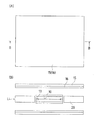
フレキシブル領域およびリジッド領域を備える従来のフレキシブルリジッドプリント配線板を図26、図27に基づいて説明する。 A conventional flexible rigid printed wiring board having a flexible region and a rigid region will be described with reference to FIGS.
図26は、従来のフレキシブルリジッド多層プリント配線板の平面図である。図27は、図26の矢符B−Bでの断面の端面を拡大して示す拡大端面図である。なお、端面図でのハッチングは図面の見易さを考慮して省略する。 FIG. 26 is a plan view of a conventional flexible rigid multilayer printed wiring board. FIG. 27 is an enlarged end view showing the end face of the cross section taken along arrow BB in FIG. It should be noted that hatching in the end view is omitted in view of easy viewing of the drawing.
4層構造として製造された従来のフレキシブルリジッド多層プリント配線板101は、概略次のような工程で製造される。
A conventional flexible rigid multilayer printed
まず、内層部材としての両面フレキシブル基板(第1層絶縁基材110および第1層導体115)を準備し内層パターン(第1層導体パターン115p)を形成する。つまり、第1層絶縁基材110に第1層導体パターン115pを形成する。なお、第1層導体パターン115pはフレキシブル領域Afでは、フレキシブルリードパターン115pfとして構成される。
First, a double-sided flexible substrate (first layer
次に、第1層導体パターン115pの表面にフィルムカバーレイを圧着する。つまり、保護絶縁膜(フィルムカバーレイ)130(保護フィルム131および保護接着剤132)を形成する。
Next, a film coverlay is pressure-bonded to the surface of the first layer conductor pattern 115p. That is, the protective insulating film (film cover lay) 130 (the
さらに、外層部材としてフレキシブル領域Afに対応する部分を除去した樹脂付き銅箔を準備し、内層部材と外層部材を積層プレスして積層(接着)する。つまり、第2層絶縁基材140、第2層導体141を積層、形成する。
Further, a copper foil with resin from which a portion corresponding to the flexible region Af is removed as an outer layer member is prepared, and the inner layer member and the outer layer member are laminated and laminated (adhered). That is, the second layer
なお、樹脂付き銅箔の代わりに外層部材としてフレキシブル領域Afに対応する部分を除去した片面リジッド基板を準備する場合もある。このときは、片面リジッド基板に対応させた接着部材を準備し、片面リジッド基板、接着部材、両面フレキシブル基板、接着部材、片面リジッド基板の順に重畳して積層プレスして積層する。 In some cases, a single-sided rigid board from which a portion corresponding to the flexible region Af is removed as an outer layer member instead of the resin-coated copper foil may be prepared. At this time, an adhesive member corresponding to the single-sided rigid substrate is prepared, and the single-sided rigid substrate, the adhesive member, the double-sided flexible substrate, the adhesive member, and the single-sided rigid substrate are superposed in order and stacked and stacked.
第2層絶縁基材140、第2層導体141を形成した後、第2層導体と第1層導体パターン115pを導通する導通孔143を開口する。全体に銅メッキして導通孔導体144を形成し、第2層導体141と第1層導体パターン115pを接続する。
After forming the second layer
次に、導通孔導体144および第2層導体141をパターニングして外層パターンを形成する。つまり、第2層導体パターン145を形成する。さらに、ソルダーレジスト150を形成し、適宜の表面処理を施す。
Next, the
その後、フレキシブル領域Afの外形を加工し、フレキシブル領域Afの外形端部Affを形成する。また、リジッド領域Arの外形を加工し、リジッド領域Arの外形端部Arfを形成する。 Thereafter, the outer shape of the flexible region Af is processed to form the outer shape end portion Aff of the flexible region Af. Further, the outer shape of the rigid region Ar is processed to form the outer edge Arf of the rigid region Ar.
外形を完成したフレキシブルリジッド多層プリント配線板101の検査を実施する(検査工程)。
Inspection of the flexible rigid multilayer printed
上述したとおり、従来のフレキシブルリジッド多層プリント配線板101は、内層部材として全面にフレキシブル基板を適用していた。
As described above, the conventional flexible rigid multilayer printed
フレキシブルリジッド多層プリント配線板101のリジッド領域Arには、多くの部品が実装される。つまり、回路配線(第2層導体パターン145)、導通孔143などが多く、高い平滑精度(例えば表面凹凸)、高い接続性能(例えば導通孔内壁の荒さ制限。一般的に導通孔内壁の凹凸が小さいほど温度衝撃による導通孔導体の金属疲労が小さく信頼性が高くなる。)などが要求される。また、高い電気性能(例えば導通抵抗、絶縁抵抗)、高い耐熱性能(例えば半田溶融耐熱)なども要求される。
Many components are mounted in the rigid region Ar of the flexible rigid multilayer printed
つまり、リジッド領域Arでは、導体は一定の厚さがある材料であり、絶縁体は一定の硬さ、一定の絶縁性がある材料であること、また、均質な材料であることが好ましい。したがって、一般的にはガラス繊維入りエポキシ樹脂が多く使われる。 That is, in the rigid region Ar, the conductor is preferably a material having a certain thickness, and the insulator is preferably a material having a certain hardness and a certain insulating property, and is preferably a homogeneous material. Therefore, in general, an epoxy resin containing glass fiber is often used.
また、フレキシブルリジッド多層プリント配線板101のフレキシブル領域Afは、リード線として機能する回路配線(フレキシブルリードパターン115pf)が多く、高い屈曲性能(例えば組み立て曲げ、開閉屈曲)などが要求される。
Further, the flexible region Af of the flexible rigid multilayer printed
つまり、フレキシブル領域Afでは、導体は一定の薄さに加工することが可能で一定の柔軟性がある材料であること、絶縁体は一定の柔軟性がある材料であることが好ましい。したがって、一般的には可撓性と絶縁性に優れたポリイミド樹脂フィルムが多く使われる。 That is, in the flexible region Af, it is preferable that the conductor is a material that can be processed to a certain thickness and has a certain flexibility, and the insulator is a material that has a certain flexibility. Therefore, in general, a polyimide resin film excellent in flexibility and insulation is often used.
しかしながら、従来のフレキシブルリジッド多層プリント配線板101は、内層部材として全面にフレキシブル基板を使用することから、リジッド領域Arでは、絶縁体がリジッド絶縁基材(第2層絶縁基材140)とフレキシブル絶縁基材(第1層絶縁基材110)の複合材料として形成されるので積層加工が難しいという問題がある。
However, since the conventional flexible rigid multilayer printed
また、リジッド領域Arが複合材料で形成されることから、導通孔の開口が難しく、導通孔導体を形成するためのメッキが難しいという問題がある。リジッド領域Arにフレキシブル絶縁基材(例えばポリイミド樹脂フィルム)が含まれることから、吸湿性が高く、耐熱性能が劣るという問題がある。 In addition, since the rigid region Ar is formed of a composite material, there is a problem that it is difficult to open the conduction hole and it is difficult to perform plating for forming the conduction hole conductor. Since a rigid insulating base (for example, a polyimide resin film) is included in the rigid region Ar, there is a problem that the hygroscopic property is high and the heat resistance performance is inferior.
さらに、リジッド領域Arの導体(第2層導体141)とフレキシブル領域Afの導体(第1層導体115)の厚さの調整が難しく、また、リジッド領域Arの導体とフレキシブル領域Afの導体の材質を最適化することが困難であるという問題がある。 Furthermore, it is difficult to adjust the thickness of the conductor (second layer conductor 141) in the rigid region Ar and the conductor (first layer conductor 115) in the flexible region Af, and the material of the conductor in the rigid region Ar and the conductor in the flexible region Af There is a problem that it is difficult to optimize.
つまり、フレキシブル領域Afおよびリジッド領域Arそれぞれに要求される積層構造特性(リジッド領域での硬質性、フレキシブル領域での可撓性、積層構造の加工容易性および信頼性、導体層特性、リジッド領域とフレキシブル領域の相互間の結合強度など)を満たすことが困難であるという問題がある。 In other words, the laminated structure characteristics required for each of the flexible region Af and the rigid region Ar (rigidity in the rigid region, flexibility in the flexible region, processability and reliability of the laminated structure, conductor layer properties, rigid region and There is a problem that it is difficult to satisfy the bonding strength between the flexible regions.
なお、リジッド領域とフレキシブル領域に異なる絶縁基材を適用する技術が提案されている(例えば特許文献1参照。)。 In addition, the technique which applies a different insulating base material to a rigid area | region and a flexible area | region is proposed (for example, refer patent document 1).
しかし、特許文献1に記載の技術では、内層パターン(第1層導体パターン)をリジッド領域とフレキシブル領域で個別に形成することから、内層パターンを高精度に位置合わせすることが困難であり微細化、高密度化が困難であるという問題がある。
本発明はこのような状況に鑑みてなされたものであり、可撓性を有するフレキシブル領域と、硬質性を有するリジッド領域とを備えるフレキシブルリジッド多層プリント配線板であって、並置したフレキシブル絶縁基材およびリジッド絶縁基材で第1層絶縁基材を構成し、重畳された複数のフレキシブル絶縁フィルムでフレキシブル絶縁基材を構成することにより、フレキシブル領域およびリジッド領域それぞれの領域に要求される積層構造特性(リジッド領域での硬質性、フレキシブル領域での可撓性、積層構造の加工容易性および信頼性、導体層特性、リジッド領域とフレキシブル領域の相互間の結合強度など)を満たした高精度で信頼性の高い高品質のフレキシブルリジッド多層プリント配線板を提供することを目的とする。 The present invention has been made in view of such a situation, and is a flexible rigid multilayer printed wiring board having a flexible region having flexibility and a rigid region having rigidity, and is a juxtaposed flexible insulating substrate. The first layer insulating base material is composed of a rigid insulating base material, and the flexible insulating base material is composed of a plurality of superposed flexible insulating films, whereby the laminated structure characteristics required for each of the flexible region and the rigid region Highly reliable with high accuracy satisfying (rigidity in rigid region, flexibility in flexible region, processability and reliability of laminated structure, conductor layer characteristics, bonding strength between rigid region and flexible region, etc.) An object of the present invention is to provide a high-quality flexible rigid multilayer printed wiring board having high performance.
また、本発明は、リジッド領域にリジッド絶縁基材、フレキシブル領域にフレキシブル絶縁基材を並置して第1層絶縁基材を構成し、第1層絶縁基材に積層された第1層導体をパターニングして第1層導体パターンとすることにより、それぞれの領域に要求される積層構造特性を満たす高精度で信頼性の高い高品質のフレキシブルリジッド多層プリント配線板の製造方法を提供することを他の目的とする。 In the present invention, a rigid insulating base is arranged in the rigid region, a flexible insulating base is juxtaposed in the flexible region to form a first layer insulating base, and the first layer conductor laminated on the first layer insulating base is provided. By providing a first layer conductor pattern by patterning, a method for producing a highly accurate and reliable high-quality flexible rigid multilayer printed wiring board that satisfies the laminated structure characteristics required for each region is provided. The purpose.
また、本発明は、本発明に係るフレキシブルリジッド多層プリント配線板を搭載した電子機器とすることにより、信頼性の高い高品質の電子機器を提供することを他の目的とする。 In addition, another object of the present invention is to provide a highly reliable electronic device with high reliability by using the flexible rigid multilayer printed wiring board according to the present invention.
本発明に係るフレキシブルリジッド多層プリント配線板は、可撓性を有するフレキシブル領域と、硬質性を有するリジッド領域とを備えるフレキシブルリジッド多層プリント配線板であって、第1層絶縁基材として並置された可撓性を有するフレキシブル絶縁基材および硬質性を有するリジッド絶縁基材と、前記第1層絶縁基材に積層された第1層導体と、前記リジッド絶縁基材に積層された第2層絶縁基材および第2層導体とを備え、前記フレキシブル絶縁基材は、重畳された複数のフレキシブル絶縁フィルムで構成してあることを特徴とする。 A flexible rigid multilayer printed wiring board according to the present invention is a flexible rigid multilayer printed wiring board including a flexible region having flexibility and a rigid region having rigidity, and is juxtaposed as a first layer insulating substrate. A flexible insulating base material having flexibility and a rigid insulating base material having rigidity, a first layer conductor laminated on the first layer insulating base material, and a second layer insulation laminated on the rigid insulating base material The flexible insulating base material includes a base material and a second layer conductor, and the flexible insulating base material includes a plurality of superimposed flexible insulating films.
この構成により、フレキシブル領域およびリジッド領域それぞれの領域に要求される積層構造特性(リジッド領域での硬質性、フレキシブル領域での可撓性、積層構造の加工容易性および信頼性、導体層特性、リジッド領域とフレキシブル領域の相互間の結合強度など)を満たした高精度で信頼性の高いフレキシブルリジッド多層プリント配線板とすることができる。 With this configuration, the laminated structure characteristics required for each of the flexible region and the rigid region (rigidity in the rigid region, flexibility in the flexible region, processability and reliability of the laminated structure, conductor layer properties, rigid A highly rigid and highly reliable flexible rigid multilayer printed wiring board satisfying the bonding strength between the region and the flexible region.
また、本発明に係るフレキシブルリジッド多層プリント配線板では、前記第1層導体は前記第1層絶縁基材の両面に積層され、前記第2層絶縁基材および第2層導体は前記第1層導体の両外側面に対称的に積層されていることを特徴とする。 In the flexible rigid multilayer printed wiring board according to the present invention, the first layer conductor is laminated on both surfaces of the first layer insulating base material, and the second layer insulating base material and the second layer conductor are the first layer. It is characterized by being laminated symmetrically on both outer sides of the conductor.
この構成により、4層構造のフレキシブルリジッド多層プリント配線板を形成することが可能となる。 With this configuration, it is possible to form a flexible rigid multilayer printed wiring board having a four-layer structure.
また、本発明に係るフレキシブルリジッド多層プリント配線板では、前記フレキシブル絶縁フィルムの相互に対向する面の外周部は、接着してあることを特徴とする。 In the flexible rigid multilayer printed wiring board according to the present invention, the outer peripheral portions of the mutually facing surfaces of the flexible insulating film are bonded.
この構成により、相互に重畳したフレキシブル絶縁フィルムの間に接着剤が侵入することを防止してフレキシブル領域の可撓性および耐屈曲性を確実に維持することが可能となる。 With this configuration, it is possible to reliably maintain the flexibility and the bending resistance of the flexible region by preventing the adhesive from entering between the flexible insulating films superimposed on each other.
また、本発明に係るフレキシブルリジッド多層プリント配線板では、前記第1層導体は銅箔で構成してあり、前記フレキシブル絶縁基材に対向する面の銅箔は前記リジッド絶縁基材に対向する面の銅箔より屈曲性を大きくしてあることを特徴とする。 In the flexible rigid multilayer printed wiring board according to the present invention, the first layer conductor is made of copper foil, and the copper foil on the surface facing the flexible insulating substrate is the surface facing the rigid insulating substrate. It is characterized in that it is more flexible than the copper foil.
この構成により、フレキシブル領域の第1層導体の可撓性をリジッド領域の第1層導体の可撓性に比較して大きくできることから、耐屈曲性、信頼性を向上させることが可能となる。 With this configuration, the flexibility of the first layer conductor in the flexible region can be increased as compared with the flexibility of the first layer conductor in the rigid region, so that the bending resistance and the reliability can be improved.
また、本発明に係るフレキシブルリジッド多層プリント配線板では、前記フレキシブル絶縁基材と前記リジッド絶縁基材の境界に対応させて前記第1層導体パターンが帯状に配置してあることを特徴とする。 The flexible rigid multilayer printed wiring board according to the present invention is characterized in that the first layer conductor pattern is arranged in a strip shape so as to correspond to a boundary between the flexible insulating substrate and the rigid insulating substrate.
この構成により、フレキシブル絶縁基材とリジッド絶縁基材の境界で相互間の結合強度(接続強度)を向上させ、フレキシブル領域およびリジッド領域の接続信頼性を向上させることが可能となる。 With this configuration, the bond strength (connection strength) between the flexible insulating base material and the rigid insulating base material can be improved, and the connection reliability between the flexible region and the rigid region can be improved.
また、本発明に係るフレキシブルリジッド多層プリント配線板の製造方法は、可撓性を有するフレキシブル領域と、硬質性を有するリジッド領域とを備えるフレキシブルリジッド多層プリント配線板の製造方法であって、可撓性を有するフレキシブル絶縁基材および硬質性を有するリジッド絶縁基材を第1層絶縁基材として並置する第1層基材並置工程と、第1層絶縁基材に第1層導体を積層する第1層導体積層工程と、前記第1層導体をパターニングして第1層導体パターンを形成する第1層パターン形成工程と、前記リジッド絶縁基材に第2層絶縁基材および第2層導体を積層する第2層積層工程とを備えることを特徴とする。 A method for manufacturing a flexible rigid multilayer printed wiring board according to the present invention is a method for manufacturing a flexible rigid multilayer printed wiring board including a flexible region having flexibility and a rigid region having rigidity. A first layer base material juxtaposition step of juxtaposing a flexible insulating base material having flexibility and a rigid insulating base material having rigidity as a first layer insulating base material, and a first layer conductor is laminated on the first layer insulating base material. A first layer conductor laminating step, a first layer pattern forming step of patterning the first layer conductor to form a first layer conductor pattern, and a second layer insulating substrate and a second layer conductor on the rigid insulating substrate. And a second layer laminating step of laminating.
この構成により、フレキシブル絶縁基材をフレキシブル領域に、リジッド絶縁基材をリジッド領域にそれぞれ対応させて並置した状態で第1層導体パターンを形成することが可能となることから、高精度に位置合わせされた第1層導体パターンをフレキシブル領域およびリジッド領域それぞれに形成し、フレキシブル領域およびリジッド領域それぞれの領域に要求される積層構造特性を満たした信頼性の高いフレキシブルリジッド多層プリント配線板を容易に生産性良く製造することができる。 With this configuration, it is possible to form the first layer conductor pattern in a state where the flexible insulating base material is aligned with the flexible region and the rigid insulating base material is aligned with the rigid region. The first layer conductor pattern is formed in each of the flexible region and rigid region, and a highly reliable flexible rigid multilayer printed wiring board that satisfies the laminated structure characteristics required for each of the flexible region and rigid region is easily produced. It can be manufactured with good performance.
また、本発明に係るフレキシブルリジッド多層プリント配線板の製造方法では、前記第1層導体を前記第1層絶縁基材の両面に積層し、前記第2層絶縁基材および前記第2層導体を前記第1層導体の両外側面に対称的に積層することを特徴とする。 In the method for manufacturing a flexible rigid multilayer printed wiring board according to the present invention, the first layer conductor is laminated on both surfaces of the first layer insulating base material, and the second layer insulating base material and the second layer conductor are provided. The first layer conductor is laminated symmetrically on both outer side surfaces.
この構成により、4層構造のフレキシブルリジッド多層プリント配線板を形成することが可能となる。 With this configuration, it is possible to form a flexible rigid multilayer printed wiring board having a four-layer structure.
また、本発明に係るフレキシブルリジッド多層プリント配線板の製造方法では、複数のフレキシブル絶縁フィルムを重畳して前記フレキシブル絶縁基材を構成することを特徴とする。 In the method for producing a flexible rigid multilayer printed wiring board according to the present invention, the flexible insulating base material is configured by superimposing a plurality of flexible insulating films.
この構成により、フレキシブル領域の柔軟性および耐屈曲性を向上させることができる。 With this configuration, flexibility and bending resistance of the flexible region can be improved.
また、本発明に係るフレキシブルリジッド多層プリント配線板の製造方法では、前記フレキシブル絶縁フィルムの相互に対向する面の外周部を予め接着することを特徴とする。 Moreover, in the manufacturing method of the flexible rigid multilayer printed wiring board concerning this invention, the outer peripheral part of the mutually opposing surface of the said flexible insulating film is adhere | attached previously.
この構成により、リジッド絶縁基材側または第1層導体側から流動してくる接着剤が相互に重畳したフレキシブル絶縁フィルムの間に侵入することを防止できるので、フレキシブル領域の可撓性および耐屈曲性を確実に維持することが可能となる。 With this configuration, it is possible to prevent the adhesive flowing from the rigid insulating base material side or the first layer conductor side from entering between the flexible insulating films superimposed on each other. It becomes possible to maintain the reliability.
また、本発明に係るフレキシブルリジッド多層プリント配線板の製造方法では、前記フレキシブル絶縁フィルムの前記第1層導体に対向する表面に予め基材接着剤層が形成してあることを特徴とする。 Moreover, in the manufacturing method of the flexible rigid multilayer printed wiring board which concerns on this invention, the base-material adhesive bond layer is previously formed in the surface facing the said 1st layer conductor of the said flexible insulating film, It is characterized by the above-mentioned.
この構成により、第1層導体を最外側のフレキシブル絶縁フィルムに確実に接着できることから、高精度の第1層導体パターンを形成することが可能となる。 With this configuration, since the first layer conductor can be reliably bonded to the outermost flexible insulating film, a highly accurate first layer conductor pattern can be formed.
また、本発明に係るフレキシブルリジッド多層プリント配線板の製造方法では、前記フレキシブル絶縁フィルムおよび前記基材接着剤層の合計層厚を前記リジッド絶縁基材の層厚より厚くすることを特徴とする。 In the method for producing a flexible rigid multilayer printed wiring board according to the present invention, the total thickness of the flexible insulating film and the base material adhesive layer is made thicker than the thickness of the rigid insulating base material.
この構成により、フレキシブル絶縁基材およびリジッド絶縁基材に対向する面で第1層導体に積層された導体接着剤層を第1層導体積層工程で押し出して薄膜化することができることから、フレキシブル領域の可撓性を向上させることが可能となる。 With this configuration, the conductive adhesive layer laminated on the first layer conductor on the surface facing the flexible insulating base and the rigid insulating base can be extruded and thinned in the first layer conductor laminating step. It becomes possible to improve the flexibility.
また、本発明に係るフレキシブルリジッド多層プリント配線板の製造方法では、前記第1層導体の前記フレキシブル絶縁基材および前記リジッド絶縁基材に対向する面に予め導体接着剤層が形成してあることを特徴とする。 In the method for producing a flexible rigid multilayer printed wiring board according to the present invention, a conductor adhesive layer is formed in advance on the surface of the first layer conductor facing the flexible insulating base material and the rigid insulating base material. It is characterized by.
この構成により、工程を簡略化して第1層導体を確実かつ容易にフレキシブル絶縁基材およびリジッド絶縁基材に接着することができるから、第1層絶縁基材での接着強度を向上させて信頼性を向上させることが可能となる。 With this configuration, the process can be simplified and the first layer conductor can be reliably and easily bonded to the flexible insulating base and the rigid insulating base. Therefore, the adhesive strength of the first layer insulating base can be improved and reliable. It becomes possible to improve the property.
また、本発明に係るフレキシブルリジッド多層プリント配線板の製造方法では、前記第1層導体の前記リジッド絶縁基材に対向する面に予め導体接着剤層が形成してあり、前記第1層導体の前記フレキシブル絶縁基材に対向する面には導体接着剤層が形成してないことを特徴とする。 Moreover, in the manufacturing method of the flexible rigid multilayer printed wiring board according to the present invention, a conductor adhesive layer is formed in advance on the surface of the first layer conductor facing the rigid insulating substrate, and the first layer conductor A conductive adhesive layer is not formed on the surface facing the flexible insulating substrate.
この構成により、フレキシブル領域を薄型化することができることから、フレキシブル領域の可撓性および耐屈曲性を向上することが可能となる。 With this configuration, the flexible region can be thinned, so that the flexibility and the bending resistance of the flexible region can be improved.
また、本発明に係るフレキシブルリジッド多層プリント配線板の製造方法では、前記リジッド絶縁基材は、半硬化接着剤層であることを特徴とする。 In the method for producing a flexible rigid multilayer printed wiring board according to the present invention, the rigid insulating base material is a semi-cured adhesive layer.
この構成により、リジッド領域でリジッド絶縁基材と第1層導体の接着を確実に行なうことができることから、リジッド領域の積層強度を向上させて信頼性を向上させることが可能となる。 With this configuration, since the rigid insulating base material and the first layer conductor can be securely bonded in the rigid region, the lamination strength of the rigid region can be improved and the reliability can be improved.
また、本発明に係るフレキシブルリジッド多層プリント配線板の製造方法では、前記第1層導体は銅箔で構成してあり、前記フレキシブル絶縁基材に対向する面の銅箔は前記リジッド絶縁基材に対向する面の銅箔より屈曲性が大きくしてあることを特徴とする。 Moreover, in the manufacturing method of the flexible rigid multilayer printed wiring board which concerns on this invention, the said 1st layer conductor is comprised with the copper foil, and the copper foil of the surface facing the said flexible insulating base material serves as the said rigid insulating base material. It is characterized in that it is more flexible than the copper foil on the opposite surface.
この構成により、フレキシブル領域の第1層導体の可撓性をリジッド領域の第1層導体の可撓性に比較して大きくできることから、耐屈曲性、信頼性を向上させることが可能となる。 With this configuration, the flexibility of the first layer conductor in the flexible region can be increased as compared with the flexibility of the first layer conductor in the rigid region, so that the bending resistance and the reliability can be improved.
また、本発明に係るフレキシブルリジッド多層プリント配線板の製造方法では、前記フレキシブル絶縁基材と前記リジッド絶縁基材の境界に対応させて前記第1層導体パターンを帯状に形成することを特徴とする。 In the method for manufacturing a flexible rigid multilayer printed wiring board according to the present invention, the first layer conductor pattern is formed in a strip shape corresponding to a boundary between the flexible insulating base material and the rigid insulating base material. .
この構成により、フレキシブル絶縁基材とリジッド絶縁基材の境界で相互間の結合強度(接続強度)を向上させ、フレキシブル領域およびリジッド領域の接続信頼性を向上させることが可能となる。 With this configuration, the bond strength (connection strength) between the flexible insulating base material and the rigid insulating base material can be improved, and the connection reliability between the flexible region and the rigid region can be improved.
また、本発明に係るフレキシブルリジッド多層プリント配線板の製造方法では、前記リジッド絶縁基材に設けた開口部に前記フレキシブル絶縁基材を嵌合することを特徴とする。 In the method for manufacturing a flexible rigid multilayer printed wiring board according to the present invention, the flexible insulating substrate is fitted into an opening provided in the rigid insulating substrate.
この構成により、リジッド領域に対するフレキシブル領域の位置合わせを自己整合的に行なうことが可能となり、リジッド領域とフレキシブル領域の接合強度を向上させ信頼性を向上させることができる。 With this configuration, the flexible region can be aligned with the rigid region in a self-aligned manner, and the bonding strength between the rigid region and the flexible region can be improved and the reliability can be improved.
また、本発明に係る電子機器は、フレキシブルリジッド多層プリント配線板を搭載した電子機器であって、前記フレキシブルリジッド多層プリント配線板は、本発明に係るフレキシブルリジッド多層プリント配線板であることを特徴とする。 The electronic device according to the present invention is an electronic device equipped with a flexible rigid multilayer printed wiring board, and the flexible rigid multilayer printed wiring board is a flexible rigid multilayer printed wiring board according to the present invention. To do.
この構成により、フレキシブル領域、リジッド領域相互間の接続強度およびフレキシブル領域の耐屈曲性が大きく、信頼性の高い高品質の電子機器とすることが可能となる。 With this configuration, the connection strength between the flexible region and the rigid region and the bending resistance of the flexible region are large, and a highly reliable electronic device with high reliability can be obtained.
本発明に係るフレキシブルリジッド多層プリント配線板によれば、可撓性を有するフレキシブル領域と、硬質性を有するリジッド領域とを備えるフレキシブルリジッド多層プリント配線板であって、並置したフレキシブル絶縁基材およびリジッド絶縁基材で第1層絶縁基材を構成し、重畳された複数のフレキシブル絶縁フィルムでフレキシブル絶縁基材を構成することから、フレキシブル領域およびリジッド領域それぞれの領域に要求される積層構造特性(リジッド領域での硬質性、フレキシブル領域での可撓性、積層構造の加工容易性および信頼性、導体層特性、リジッド領域とフレキシブル領域の相互間の結合強度など)を満たし、高精度で信頼性の高い高品質のフレキシブルリジッド多層プリント配線板とすることができるという効果を奏する。 According to the flexible rigid multilayer printed wiring board according to the present invention, a flexible rigid multilayer printed wiring board including a flexible region having flexibility and a rigid region having rigidity, the flexible insulating base material and the rigid being juxtaposed. The first layer insulating base material is composed of an insulating base material, and the flexible insulating base material is composed of a plurality of superimposed flexible insulating films. Therefore, the laminated structure characteristics (rigid) required for each of the flexible region and the rigid region High rigidity and flexibility, flexibility in the flexible area, ease of processing and reliability of the laminated structure, conductor layer characteristics, bonding strength between the rigid area and the flexible area, etc. The effect of being able to be a high-quality flexible rigid multilayer printed wiring board Unlikely to.
本発明に係るフレキシブルリジッド多層プリント配線板の製造方法によれば、リジッド領域にリジッド絶縁基材、フレキシブル領域にフレキシブル絶縁基材を並置して第1層絶縁基材を構成し、第1層絶縁基材に積層された第1層導体をパターニングして第1層導体パターンとすることから、高精度でそれぞれの領域に要求される積層構造特性を満たす信頼性の高い高品質のフレキシブルリジッド多層プリント配線板を容易に生産性良く製造できるという効果を奏する。 According to the method for manufacturing a flexible rigid multilayer printed wiring board according to the present invention, a rigid insulating base material is juxtaposed in a rigid region, and a flexible insulating base material is juxtaposed in a flexible region to form a first layer insulating base material. Since the first layer conductor layered on the base material is patterned to form the first layer conductor pattern, highly reliable and flexible flexible rigid multi-layer print that satisfies the laminated structure characteristics required for each region with high accuracy There is an effect that the wiring board can be easily manufactured with high productivity.
本発明に係る電子機器によれば、本発明に係るフレキシブルリジッド多層プリント配線板を搭載することから、フレキシブル領域、リジッド領域相互間の接続強度およびフレキシブル領域の耐屈曲性が大きく、信頼性の高い高品質の電子機器とすることができるという効果を奏する。 According to the electronic device according to the present invention, since the flexible rigid multilayer printed wiring board according to the present invention is mounted, the flexible region, the connection strength between the rigid regions, and the bending resistance of the flexible region are large and highly reliable. There exists an effect that it can be set as a high quality electronic device.
以下、本発明の実施の形態を図面に基づいて説明する。 Hereinafter, embodiments of the present invention will be described with reference to the drawings.
<実施の形態1>
本発明に係るフレキシブルリジッド多層プリント配線板の製造方法の概略を実施の形態1として図1A、図1Bに基づいて説明する。
<Embodiment 1>
The outline of the manufacturing method of the flexible rigid multilayer printed wiring board concerning this invention is demonstrated as Embodiment 1 based on FIG. 1A and FIG. 1B.
図1A、図1Bは、本発明の実施の形態1に係るフレキシブルリジッド多層プリント配線板の製造方法の工程フローを概略的に示すフロー図である。 1A and 1B are flowcharts schematically showing a process flow of a method for manufacturing a flexible rigid multilayer printed wiring board according to Embodiment 1 of the present invention.
本実施の形態に係るフレキシブルリジッド多層プリント配線板の製造方法は、可撓性を有するフレキシブル領域と、硬質性を有するリジッド領域とを備えるフレキシブルリジッド多層プリント配線板を製造する方法に関する。 The manufacturing method of the flexible rigid multilayer printed wiring board which concerns on this Embodiment is related with the method of manufacturing a flexible rigid multilayer printed wiring board provided with the flexible area | region which has flexibility, and the rigid area | region which has rigidity.
工程S1:
第1層絶縁基材を準備する。つまり、可撓性を有するフレキシブル絶縁基材および硬質性を有するリジッド絶縁基材を第1層絶縁基材として並置する(第1層基材並置工程。図2参照。)。例えば、リジッド絶縁基材を打ち抜いて設けた開口部にフレキシブル絶縁基材を嵌合する(フレキシブル絶縁基材嵌合工程ともいう。)ことにより第1層絶縁基材を構成する。
Step S1:
A first layer insulating substrate is prepared. That is, the flexible insulating base material having flexibility and the rigid insulating base material having flexibility are juxtaposed as the first layer insulating base material (first layer base material juxtaposition step, see FIG. 2). For example, the first insulating layer is configured by fitting a flexible insulating substrate into an opening provided by punching out a rigid insulating substrate (also referred to as a flexible insulating substrate fitting step).
フレキシブル絶縁基材の大きさをリジッド絶縁基材の開口部の内側に近接して収容できる大きさとして嵌合することにより、リジッド領域に対するフレキシブル領域の位置合わせを自己整合的に行なうことが可能となり、リジッド領域とフレキシブル領域の位置合わせ精度および接合強度を向上させて信頼性を向上させることができる。 By fitting the size of the flexible insulating base so that it can be accommodated close to the inside of the opening of the rigid insulating base, it becomes possible to align the flexible region with the rigid region in a self-aligning manner. In addition, it is possible to improve the alignment accuracy and the bonding strength between the rigid region and the flexible region, thereby improving the reliability.
工程S2:
第1層絶縁基材に積層する第1層導体を準備する(第1層導体準備工程)。例えば、樹脂付き銅箔(RCC:Resin Coated Cupper。図3参照。)を適用することが可能である。
Step S2:
A first layer conductor to be laminated on the first layer insulating base material is prepared (first layer conductor preparation step). For example, a resin-coated copper foil (RCC: Resin Coated Copper; see FIG. 3) can be applied.
工程S3:
第1層絶縁基材に第1層導体を重畳(位置合わせ)する(第1層導体重畳工程。図4参照。)。つまり、例えばワークの4隅に設けた位置合わせガイド(図18参照。)を適用することにより、第1層絶縁基材に対して第1層導体を位置合わせする。
Step S3:
The first layer conductor is superimposed (positioned) on the first layer insulating substrate (first layer conductor overlapping step, see FIG. 4). That is, for example, by applying alignment guides (see FIG. 18) provided at the four corners of the workpiece, the first layer conductor is aligned with respect to the first layer insulating substrate.
なお、第1層導体を第1層絶縁基材の両面に積層して多層化(4層化)することが可能である。この場合は、第1層絶縁基材および第1層導体が外層に対する内層となる。 The first layer conductor can be laminated on both surfaces of the first layer insulating base material to form a multilayer (four layers). In this case, the first layer insulating base material and the first layer conductor serve as an inner layer with respect to the outer layer.
工程S4:
第1層絶縁基材と第1層導体を積層(接着)する。つまり、第1層絶縁基材(フレキシブル絶縁基材およびリジッド絶縁基材)に第1層導体を積層する(第1層導体積層工程。図5参照。)。例えば、真空プレスなどで積層(積層プレス)することにより、第1層絶縁基材に第1層導体を積層接着する。なお、第1層導体重畳工程は、第1層導体積層工程の一部として把握することも可能である。
Step S4:
The first layer insulating substrate and the first layer conductor are laminated (adhered). That is, a 1st layer conductor is laminated | stacked on a 1st layer insulation base material (a flexible insulation base material and a rigid insulation base material) (1st layer conductor lamination process. Refer FIG. 5). For example, the first layer conductor is laminated and bonded to the first layer insulating substrate by laminating (laminating press) with a vacuum press or the like. The first layer conductor superimposing step can be grasped as a part of the first layer conductor stacking step.
工程S5:
第1層導体をパターニングして第1層導体パターンを形成する(第1層パターン形成工程。図6参照。)。例えば、公知のエッチング技術を適用することが可能である。
Step S5:
The first layer conductor is patterned to form a first layer conductor pattern (first layer pattern forming step, see FIG. 6). For example, a known etching technique can be applied.
この構成により、フレキシブル絶縁基材をフレキシブル領域に、リジッド絶縁基材をリジッド領域にそれぞれ対応させて並置した状態で第1層導体パターンを形成することが可能となることから、高精度に位置合わせされた第1層導体パターンをフレキシブル領域およびリジッド領域それぞれに形成し、フレキシブル領域およびリジッド領域それぞれの領域に要求される積層構造特性(リジッド領域での硬質性、フレキシブル領域での可撓性、積層構造の加工容易性および信頼性、導体層特性、リジッド領域とフレキシブル領域の相互間の結合強度など)を満たした高精度で信頼性の高い高品質のフレキシブルリジッド多層プリント配線板を製造することができる。 With this configuration, it is possible to form the first layer conductor pattern in a state where the flexible insulating base material is aligned with the flexible region and the rigid insulating base material is aligned with the rigid region. The first layer conductor pattern is formed in each of the flexible region and the rigid region, and the laminated structure characteristics required for each of the flexible region and the rigid region (rigidity in the rigid region, flexibility in the flexible region, lamination) Manufacturing high-precision, reliable, high-quality flexible rigid multi-layer printed wiring boards that satisfy the processability and reliability of the structure, conductor layer characteristics, bond strength between the rigid and flexible regions, etc.) it can.
工程S6:
フレキシブル領域で第1層導体パターンに保護絶縁層を積層する。例えば、保護絶縁層としてのフィルムカバーレイを圧着する(フレキシブル領域保護層形成工程。図7参照。)。フィルムカバーレイは、例えばカバーレイフィルム12.5μmに接着剤15μmを塗布したものを、フレキシブル領域の形状に合わせて加工し、フレキシブル領域に位置合わせして仮止め(例えば、半田ごてやアイロンなどでの加熱による仮固定)し、さらに例えば真空プレスなどで積層(積層プレス)する。
Step S6:
A protective insulating layer is laminated on the first layer conductor pattern in the flexible region. For example, a film cover lay as a protective insulating layer is pressure-bonded (flexible region protective layer forming step, see FIG. 7). The film coverlay is, for example, a coverlay film of 12.5 μm coated with an adhesive of 15 μm, processed according to the shape of the flexible region, and aligned to the flexible region and temporarily fixed (for example, a soldering iron or iron For example, by vacuum pressing or the like (stacking press).
工程S7:
第2層絶縁基材および第2層導体を準備する。つまり、フレキシブル領域に対応する部分を除去(開口)して開口部を設け、リジッド領域に対応した形状とする(図8参照。)。なお、第1層導体積層工程と同様に、例えば樹脂付き銅箔を適用することが可能である。樹脂付き銅箔は、例えば電解銅箔18μmにエポキシ系樹脂50μmを積層したものとする。
Step S7:
A second layer insulating substrate and a second layer conductor are prepared. That is, a portion corresponding to the flexible region is removed (opened) to provide an opening, and a shape corresponding to the rigid region is formed (see FIG. 8). In addition, it is possible to apply resin-coated copper foil, for example, similarly to the first layer conductor lamination step. The copper foil with resin is obtained by, for example, laminating an
工程S8:
リジッド領域で第2層絶縁基材および第2層導体を重畳(位置合わせ)する(第2層重畳工程。図9参照。)。つまり、例えばワークの4隅に設けた位置合わせガイドを適用することにより、第2層絶縁基材、第2層導体を第1絶縁基材、第1層導体に対して位置合わせする。
Step S8:
The second layer insulating base material and the second layer conductor are superimposed (aligned) in the rigid region (second layer overlapping step, see FIG. 9). That is, for example, by applying alignment guides provided at the four corners of the workpiece, the second layer insulating base material and the second layer conductor are aligned with the first insulating base material and the first layer conductor.
なお、第2層絶縁基材および第2層導体を第1層導体(第1層絶縁基材)の両外側面に対称的に積層して多層化(4層化)することが可能である。この場合は、第2層絶縁基材および第2層導体が第1層絶縁基材および第1層導体で構成される内層に対する外層となる。 The second layer insulating base material and the second layer conductor can be multilayered (four layers) by symmetrically laminating on both outer surfaces of the first layer conductor (first layer insulating base material). . In this case, the second layer insulating base material and the second layer conductor are outer layers with respect to the inner layer composed of the first layer insulating base material and the first layer conductor.
工程S9:
リジッド領域で第2層絶縁基材および第2層導体を積層(接着)する。つまり、リジッド絶縁基材に第2層絶縁基材および第2層導体を積層する(第2層積層工程。図10参照。)。例えば、真空プレスなどで積層(積層プレス)することにより、第1層絶縁基材および第1層導体に第2層絶縁基材および第2層導体を積層接着する。なお、第2層重畳工程は、第2層積層工程の一部として把握することも可能である。
Step S9:
The second layer insulating base material and the second layer conductor are laminated (adhered) in the rigid region. That is, a 2nd layer insulation base material and a 2nd layer conductor are laminated | stacked on a rigid insulation base material (2nd layer lamination process. Refer FIG. 10). For example, the second layer insulating base material and the second layer conductor are laminated and bonded to the first layer insulating base material and the first layer conductor by laminating (laminating press) with a vacuum press or the like. The second layer superimposing step can be grasped as a part of the second layer stacking step.
工程S10:
第2層導体と第1層導体パターンを導通する導通孔を開口する。つまり、第1層導体パターンにつながる導通孔を第2層導体および第2層絶縁基材を通して開口する(導通孔開口工程。図11参照。)。例えばレーザー加工を施すことにより導通孔を開口することが可能である。レーザー加工は、第2層導体の導通孔部分を始めに除去し、次に第2層絶縁基材の導通孔部分を除去しても良く、また、第2層導体と第2層絶縁基材を同時に除去しても良い。
Step S10:
A conduction hole for conducting the second layer conductor and the first layer conductor pattern is opened. That is, the conduction hole connected to the first layer conductor pattern is opened through the second layer conductor and the second layer insulating base material (conduction hole opening step; see FIG. 11). For example, it is possible to open the conduction hole by performing laser processing. In the laser processing, the conduction hole portion of the second layer conductor may be removed first, and then the conduction hole portion of the second layer insulating base material may be removed. Also, the second layer conductor and the second layer insulating base material may be removed. May be removed simultaneously.
工程S11:
導通孔に導通孔導体を形成する。つまり、導通孔の少なくとも底面および側壁を充填する導体層(導通孔導体)を形成して第2層導体と第1層導体パターンを接続する(導通孔導体形成工程。図12参照。)。例えば全面に銅メッキを施すことにより導通孔導体を形成することが可能である。
Step S11:
A conduction hole conductor is formed in the conduction hole. That is, a conductor layer (conduction hole conductor) filling at least the bottom surface and the side wall of the conduction hole is formed and the second layer conductor and the first layer conductor pattern are connected (conduction hole conductor forming step, see FIG. 12). For example, it is possible to form a conduction hole conductor by performing copper plating on the entire surface.
工程S12:
第2層導体(および導通孔導体)をパターニングして第2層導体パターンを形成する(第2層パターン形成工程。図13参照。)。例えば公知のエッチング技術を適用することが可能である。
Step S12:
The second layer conductor (and the conduction hole conductor) is patterned to form a second layer conductor pattern (second layer pattern forming step, see FIG. 13). For example, a known etching technique can be applied.
工程S13:
第2層導体パターンをソルダーレジストで被覆し、ソルダーレジストをパターニングする。つまり、公知の技術を適用してソルダーレジストに必要な開口部を設ける(ソルダ−レジスト形成工程。図14参照。)。ソルダーレジストとしては、例えばエポキシ系フォトソルダーレジストを適用することが可能である。
Step S13:
The second layer conductor pattern is covered with a solder resist, and the solder resist is patterned. That is, a known technique is applied to provide a necessary opening for the solder resist (solder-resist forming step, see FIG. 14). As the solder resist, for example, an epoxy photo solder resist can be applied.
工程S14:
ソルダーレジストの開口部の第2層導体パターンに表面処理を施す(表面処理工程)。表面処理としては、例えばソルダーレジストの開口部に露出した第2層導体パターンに無電解ニッケル金メッキを施すことなどが可能である。
Step S14:
A surface treatment is applied to the second layer conductor pattern in the opening of the solder resist (surface treatment step). As the surface treatment, for example, electroless nickel gold plating can be applied to the second layer conductor pattern exposed in the opening of the solder resist.
工程S15:
フレキシブル領域の外形を加工する(フレキシブル領域外形加工工程。図15参照。)。例えば金型などを適用してフレキシブル領域の外形を打ち抜きプレスにより加工する。
Step S15:
The outer shape of the flexible region is processed (flexible region outer shape processing step, see FIG. 15). For example, the outer shape of the flexible region is processed by a punching press using a mold or the like.
工程S16:
リジッド領域の外形を加工する(リジッド領域外形加工工程。図16参照。)。フレキシブル領域外形加工工程と同様に、例えば金型などを適用してリジッド領域の外形を打ち抜きプレスにより加工する。
Step S16:
The outer shape of the rigid region is processed (rigid region outer shape processing step; see FIG. 16). Similarly to the flexible region outer shape processing step, the outer shape of the rigid region is processed by a punching press using, for example, a mold.
工程S17:
処理工程を終了したフレキシブルリジッド多層プリント配線板を検査する(検査工程)。例えば電気的特性を検査する電気検査、外観形状を検査する外観検査などを行なうことが可能である。
Step S17:
The flexible rigid multilayer printed wiring board that has finished the processing step is inspected (inspection step). For example, it is possible to perform an electrical inspection for inspecting electrical characteristics, an appearance inspection for inspecting the appearance shape, and the like.
上述したとおり、本実施の形態に係るフレキシブルリジッド多層プリント配線板の製造方法によれば、フレキシブル領域およびリジッド領域それぞれの領域に要求される積層構造特性を満たした信頼性の高いフレキシブルリジッド多層プリント配線板を容易に生産性良く製造することができる。 As described above, according to the method for manufacturing a flexible rigid multilayer printed wiring board according to the present embodiment, a flexible flexible multilayer printed wiring having high reliability that satisfies the laminated structure characteristics required for each of the flexible region and the rigid region. The plate can be easily manufactured with high productivity.
<実施の形態2>
実施の形態1の具体例として、4層構造でフォールディング仕様としたフレキシブルリジッドプリント配線板およびその製造方法を本発明に係る実施の形態2として図2ないし図18に基づいて説明する。なお、基本的には、実施の形態1に係るフレキシブルリジッド多層プリント配線板(およびその製造方法)と同様であるので重複する事項については適宜説明を省略する。
<Embodiment 2>
As a specific example of the first embodiment, a flexible rigid printed wiring board having a four-layer structure and a folding specification and a manufacturing method thereof will be described as a second embodiment of the present invention with reference to FIGS. In addition, since it is the same as that of the flexible rigid multilayer printed wiring board (and its manufacturing method) which concerns on Embodiment 1, it abbreviate | omits description about the matter which overlaps suitably.
また、図2ないし図16は、リジッド領域とフレキシブル領域との境界を拡大して示し、図17は、実際のフレキシブルリジッド多層プリント配線板のレイアウト例を示し、図18は、フレキシブルリジッド多層プリント配線板を製造するときに適用するワーク例を示す。 2 to 16 show an enlarged boundary between the rigid region and the flexible region, FIG. 17 shows an example layout of an actual flexible rigid multilayer printed wiring board, and FIG. 18 shows a flexible rigid multilayer printed wiring. The example of a workpiece | work applied when manufacturing a board is shown.
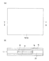
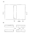
図2は、本発明の実施の形態2に係るフレキシブルリジッド多層プリント配線板の第1層絶縁基材の構成概要を説明する説明図であり、(A)は平面図、(B)は(A)の矢符B−Bでの断面の端面を示す端面図である。なお、端面図でのハッチングは図面の見易さを考慮して省略する(以下同様とする。)。 2A and 2B are explanatory views for explaining the outline of the configuration of the first layer insulating base material of the flexible rigid multilayer printed wiring board according to Embodiment 2 of the present invention. FIG. 2A is a plan view, and FIG. It is an end view which shows the end surface of the cross section by arrow BB of). It should be noted that hatching in the end view is omitted for the sake of easy viewing (hereinafter the same shall apply).
フレキシブル領域Afに対応するフレキシブル絶縁基材10、リジッド領域Arに対応するリジッド絶縁基材20を準備する。フレキシブル絶縁基材10およびリジッド絶縁基材20は、平面状に相互に並置され第1層絶縁基材Liを構成する(第1層基材並置工程)。フレキシブル絶縁基材10の外形とリジッド絶縁基材20を開口して設けた開口部20wは、相互に整合するように形成してあり、フレキシブル絶縁基材10は開口部20wに自己整合的に嵌合できる構成としてある(フレキシブル絶縁基材嵌合工程ともいう。)。
A flexible insulating
なお、フレキシブル絶縁基材10とリジッド絶縁基材20の間隔は、高々数十μm程度としてあり、後工程の第1層導体積層工程(図5参照。)で周囲から流動してくる接着剤で相互に接着される。したがって、リジッド領域Arとフレキシブル領域Afの接合強度を確保して信頼性を向上させることができる。
The distance between the flexible insulating
リジッド絶縁基材20は、半硬化性接着剤層(プリプレグ)としてあり、例えばガラス繊維強化エポキシ樹脂の半硬化接着剤(例えば50μm)で構成される。リジッド領域Arでリジッド絶縁基材20と第1層導体15(図3参照。)の接着を確実に行なうことができることから、リジッド領域Arの積層強度を向上させて信頼性を向上させることが可能となる。
The rigid
フレキシブル絶縁基材10は、複数のフレキシブル絶縁フィルム11を重畳してある。例えば2枚のフレキシブル絶縁フィルム11でフレキシブル絶縁基材10を構成することから、フレキシブル領域Afの柔軟性および耐屈曲性を向上させることができる。フレキシブル絶縁フィルム11は、例えばポリイミドフィルム25μmで構成される。
The flexible insulating
フレキシブル絶縁フィルム11の第1層導体15に対向する表面に、予め基材接着剤層12を形成(積層)しておく。基材接着剤層12は、例えばエポキシ系樹脂接着剤層15μmをフレキシブル絶縁フィルム11に塗布して形成する。この構成により、第1層導体15を最外側のフレキシブル絶縁フィルム11に確実に接着できることから、高精度の第1層導体パターン15p(図6参照。)を形成することが可能となる。
A
また、フレキシブル絶縁フィルム11および基材接着剤層12でフレキシブル絶縁基材10を構成する。この構成により、第1層絶縁基材Liでのフレキシブル領域Afの厚さをリジッド領域Arの厚さより厚くし、フレキシブル絶縁基材10およびリジッド絶縁基材20に対向する面で第1層導体15に積層された接着剤層16(図3参照。)を第1層導体積層工程(図5参照。)で押し出して薄膜化することができることから、フレキシブル領域Afの可撓性をさらに向上させることが可能となる。
In addition, the flexible insulating
なお、フレキシブル絶縁フィルム11の相互に対向する面の外周部を接着剤13で予め接着しておく。接着剤13は、例えばエポキシ系樹脂接着剤層4μmとして構成する。この構成により、第1層導体積層工程で、リジッド絶縁基材20側または第1層導体15側から流動してくる接着剤が相互に重畳したフレキシブル絶縁フィルム11の間に侵入することを防止できるので、フレキシブル領域Afの可撓性および耐屈曲性を確実に維持することが可能となる。
In addition, the outer peripheral part of the mutually opposing surface of the flexible insulating
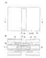
図3は、本発明の実施の形態2に係るフレキシブルリジッド多層プリント配線板の第1層導体の構成概要を説明する説明図であり、(A)は平面図、(B)は(A)の矢符B−Bでの断面の端面を示す端面図である。 3A and 3B are explanatory diagrams for explaining the outline of the configuration of the first layer conductor of the flexible rigid multilayer printed wiring board according to Embodiment 2 of the present invention. FIG. 3A is a plan view, and FIG. It is an end view which shows the end surface of the cross section by arrow BB.
第1層導体15を第1層絶縁基材Liの両面に対応させて準備する(第1層導体準備工程)。第1層絶縁基材Liに積層する第1層導体15は、例えば電解銅箔18μmで構成してあり、フレキシブル絶縁基材10およびリジッド絶縁基材20に対向する面に予め接着剤(導体接着剤層16)が形成してある。導体接着剤層16は、例えばエポキシ系樹脂接着剤層50μmで構成してあり、第1層導体15および導体接着剤層16は、一般に樹脂付き銅箔(RCC)として市販されているものを適用することができる。
The
この構成により、第1層導体15を確実かつ容易にフレキシブル絶縁基材10およびリジッド絶縁基材20に接着することができるから、第1層絶縁基材Liでの接着強度を向上させて信頼性を向上させることが可能となる。
With this configuration, the
なお、第1層導体15および導体接着剤層16は、第1層絶縁基材Liの両面に対称的に配置して多層(4層)構造の内層を構成するように2枚準備する。
In addition, the
図4は、本発明の実施の形態2に係るフレキシブルリジッド多層プリント配線板の第1層導体を第1層絶縁基材に重畳した状態を説明する説明図であり、(A)は平面図、(B)は(A)の矢符B−Bでの断面の端面を示す端面図である。 FIG. 4 is an explanatory diagram for explaining a state in which the first layer conductor of the flexible rigid multilayer printed wiring board according to Embodiment 2 of the present invention is superimposed on the first layer insulating substrate, (A) is a plan view, (B) is an end elevation showing an end face of a cross section at arrow BB in (A).
第1層絶縁基材Liに第1層導体15および導体接着剤層16を重畳して位置合わせを行なう(第1層導体重畳工程)。
The
図5は、本発明の実施の形態2に係るフレキシブルリジッド多層プリント配線板の第1層導体を第1層絶縁基材に積層した状態を説明する説明図であり、(A)は平面図、(B)は(A)の矢符B−Bでの断面の端面を示す端面図である。 FIG. 5 is an explanatory view for explaining a state in which the first layer conductor of the flexible rigid multilayer printed wiring board according to Embodiment 2 of the present invention is laminated on the first layer insulating substrate, (A) is a plan view, (B) is an end elevation showing an end face of a cross section at arrow BB in (A).
第1層絶縁基材Liに重畳した第1層導体15および導体接着剤層16を積層プレスして積層(接着)する(第1層導体積層工程)。
The
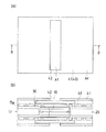
図6は、本発明の実施の形態2に係るフレキシブルリジッド多層プリント配線板の第1層導体をパターニングした状態を説明する説明図であり、(A)は平面図、(B)は(A)の矢符B−Bでの断面の端面を示す端面図である。 6A and 6B are explanatory diagrams for explaining a state in which the first layer conductor of the flexible rigid multilayer printed wiring board according to Embodiment 2 of the present invention is patterned. FIG. 6A is a plan view, and FIG. It is an end elevation which shows the end surface of the cross section by arrow BB of.
公知の技術を適用して第1層導体15をパターニングして、第1層導体パターン15pを形成する(第1層パターン形成工程)。第1層導体パターン15pは、フレキシブル絶縁基材10およびリジッド絶縁基材20に対応して形成され、フレキシブル絶縁基材10にはリード線として機能するフレキシブルリードパターン15pfが併せて形成される。
The
また、フレキシブル絶縁基材10とリジッド絶縁基材20の境界に対応させて第1層導体パターンを帯状に形成した帯状保護パターン15pgを併せて形成する。帯状パターン15pgにより、フレキシブル絶縁基材10とリジッド絶縁基材20の境界で相互間の結合強度(接続強度)を向上させ、フレキシブル領域Afおよびリジッド領域Arの接続信頼性を向上させることが可能となる。
A band-shaped protective pattern 15pg in which the first layer conductor pattern is formed in a band shape corresponding to the boundary between the flexible insulating
図7は、本発明の実施の形態2に係るフレキシブルリジッド多層プリント配線板の第1層導体パターンを保護する保護絶縁層を積層した状態を説明する説明図であり、(A)は平面図、(B)は(A)の矢符B−Bでの断面の端面を示す端面図である。 FIG. 7 is an explanatory view for explaining a state in which a protective insulating layer for protecting the first layer conductor pattern of the flexible rigid multilayer printed wiring board according to Embodiment 2 of the present invention is laminated, (A) is a plan view, (B) is an end elevation showing an end face of a cross section at arrow BB in (A).
フレキシブル絶縁基材10を保護する保護絶縁層30をフレキシブル領域Afに形成(積層)する(フレキシブル領域保護層形成工程)。保護絶縁層30は、保護フィルム31および保護接着剤32で構成してある。保護絶縁層30は、例えばフィルムカバーレイを適用して形成することが可能であり、予めフレキシブル領域Afに対応する形状に成形した後、位置合わせして接着する。
A protective insulating
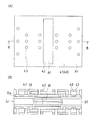
図8は、本発明の実施の形態2に係るフレキシブルリジッド多層プリント配線板の第2層絶縁基材および第2層導体の構成概要を説明する説明図であり、(A)は平面図、(B)は(A)の矢符B−Bでの断面の端面を示す端面図である。 FIG. 8 is an explanatory view for explaining the configuration outline of the second layer insulating base material and the second layer conductor of the flexible rigid multilayer printed wiring board according to Embodiment 2 of the present invention, (A) is a plan view, B) is an end view showing an end face of a cross section taken along arrows BB in (A).
リジッド絶縁基材20に第2層絶縁基材40および第2層導体41を第1層導体15(第1層導体パターン15p)に対応させて準備する(第2層準備工程)。第2層絶縁基材40および第2層導体41には、フレキシブル領域Afに対応する開口部42が予め形成してあり、リジッド絶縁基材20に積層する構成としておく。第2層絶縁基材40および第2層導体41は、第1層導体15と同様に樹脂付き銅箔(RCC)として提供されているものを適用することができる。
The second insulating
なお、第2層絶縁基材40および第2層導体41は、第1層導体15(第1層導体パターン15p)の両外側面に対称的に配置して多層(4層)構造とするために2枚準備する。
The second-layer
図9は、本発明の実施の形態2に係るフレキシブルリジッド多層プリント配線板の第2層絶縁基材および第2層導体をリジッド絶縁基材に重畳した状態を説明する説明図であり、(A)は平面図、(B)は(A)の矢符B−Bでの断面の端面を示す端面図である。 FIG. 9 is an explanatory diagram for explaining a state in which the second layer insulating base material and the second layer conductor of the flexible rigid multilayer printed wiring board according to Embodiment 2 of the present invention are superimposed on the rigid insulating base material. ) Is a plan view, and (B) is an end view showing an end face of a cross section taken along arrows BB in (A).
リジッド絶縁基材20(リジッド領域Ar)に第2層絶縁基材40および第2層導体41を重畳して位置合わせを行なう(第2層重畳工程)。
The second layer insulating
図10は、本発明の実施の形態2に係るフレキシブルリジッド多層プリント配線板の第2層絶縁基材および第2層導体をリジッド絶縁基材に積層した状態を説明する説明図であり、(A)は平面図、(B)は(A)の矢符B−Bでの断面の端面を示す端面図である。 FIG. 10 is an explanatory diagram for explaining a state in which the second layer insulating base material and the second layer conductor of the flexible rigid multilayer printed wiring board according to Embodiment 2 of the present invention are laminated on the rigid insulating base material. ) Is a plan view, and (B) is an end view showing an end face of a cross section taken along arrows BB in (A).
リジッド絶縁基材20(リジッド領域Ar)に重畳した第2層絶縁基材40および第2層導体41を積層プレスして積層(接着)する(第2層積層工程)。
The second layer insulating
図11は、本発明の実施の形態2に係るフレキシブルリジッド多層プリント配線板の第2層導体と第1層導体パターンの間の導通孔を形成した状態を説明する説明図であり、(A)は平面図、(B)は(A)の矢符B−Bでの断面の端面を示す端面図である。 FIG. 11 is an explanatory view illustrating a state in which a conduction hole is formed between the second layer conductor and the first layer conductor pattern of the flexible rigid multilayer printed wiring board according to Embodiment 2 of the present invention. Is a plan view, and (B) is an end view showing an end face of a cross section taken along arrows BB in (A).
第2層導体41と第1層導体パターン15pを導通する導通孔43を公知の技術を適用して開口する(導通孔開口工程)。
A
図12は、本発明の実施の形態2に係るフレキシブルリジッド多層プリント配線板の導通孔に導通孔導体を形成した状態を説明する説明図であり、(A)は平面図、(B)は(A)の矢符B−Bでの断面の端面を示す端面図である。 12A and 12B are explanatory views for explaining a state in which a conduction hole conductor is formed in the conduction hole of the flexible rigid multilayer printed wiring board according to the second embodiment of the present invention. FIG. 12A is a plan view, and FIG. It is an end view which shows the end surface of the cross section by arrow BB of A).
公知の技術を適用して導通孔43に導通孔導体44を形成する(導通孔導体形成工程)。つまり、導通孔43の少なくとも底面および側壁を充填する導体層(導通孔導体44)を形成して第2層導体41と第1層導体パターン15pを接続する。
By applying a known technique, the
図13は、本発明の実施の形態2に係るフレキシブルリジッド多層プリント配線板の導通孔導体および第2層導体をパターニングして第2層導体パターンを形成した状態を説明する説明図であり、(A)は平面図、(B)は(A)の矢符B−Bでの断面の端面を示す端面図である。 FIG. 13 is an explanatory diagram for explaining a state where the second layer conductor pattern is formed by patterning the conduction hole conductor and the second layer conductor of the flexible rigid multilayer printed wiring board according to Embodiment 2 of the present invention. (A) is a plan view, (B) is an end view showing an end face of a cross section at arrow BB in (A).
公知の技術を適用して導通孔導体44および第2層導体41をパターニングして第2層導体パターン45を形成する(第2層パターン形成工程)。導通孔43では第2層導体パターン45と第1層導体パターン15pとが接続され、第2層導体パターン45として必要な接続配線が形成される。
By applying a known technique, the
図14は、本発明の実施の形態2に係るフレキシブルリジッド多層プリント配線板の第2層導体パターンにソルダーレジストを形成した状態を説明する説明図であり、(A)は平面図、(B)は(A)の矢符B−Bでの断面の端面を示す端面図である。 FIG. 14 is an explanatory view for explaining a state in which a solder resist is formed on the second layer conductor pattern of the flexible rigid multilayer printed wiring board according to Embodiment 2 of the present invention, (A) is a plan view, and (B). [FIG. 4] An end view showing an end face of a cross section taken along arrows BB in (A).
第2層導体パターン45をソルダーレジスト50で被覆し、ソルダーレジスト50をパターニングする(ソルダ−レジスト形成工程)。したがって、公知の技術を適用してソルダーレジスト50に所定の開口部50wを設けるが可能となる。
The second
つまり、フレキシブル絶縁基材10に対応する領域では開口部50wを形成してフレキシブル領域Afの可撓性を確保し、リジッド絶縁基材20に対応する領域では積層したソルダーレジスト50により第2層導体パターン45を保護する。また、第2層導体パターン45に対する接続が必要な箇所(部品実装端子45pt。図17参照。)では、開口部50wを形成して部品実装端子45ptを露出させる。
That is, the
次に、リジッド領域Ar(Ar1、Ar2。図17参照。)で開口部50wから露出している第2層導体パターン45(部品実装端子45pt)に表面処理を施す(表面処理工程)。
Next, surface treatment is applied to the second layer conductor pattern 45 (component mounting terminal 45pt) exposed from the
図15は、本発明の実施の形態2に係るフレキシブルリジッド多層プリント配線板のフレキシブル領域の外形を形成した状態を説明する説明図であり、(A)は平面図、(B)は(A)の矢符B−Bでの断面の端面を示す端面図である。 15A and 15B are explanatory views for explaining a state in which the outer shape of the flexible region of the flexible rigid multilayer printed wiring board according to the second embodiment of the present invention is formed. FIG. 15A is a plan view, and FIG. It is an end elevation which shows the end surface of the cross section by arrow BB of.
フレキシブル領域Afの外形を加工し、フレキシブル領域Afの外形端部Affを例えば金型による打ち抜きで形成する(フレキシブル領域外形加工工程)。 The outer shape of the flexible region Af is processed, and the outer end Aff of the flexible region Af is formed by, for example, punching with a mold (flexible region outer shape processing step).
図16は、本発明の実施の形態2に係るフレキシブルリジッド多層プリント配線板のリジッド領域の外形を形成した状態を説明する説明図であり、(A)は平面図、(B)は(A)の矢符B−Bでの断面の端面を示す端面図である。 FIGS. 16A and 16B are explanatory diagrams for explaining a state in which the outer shape of the rigid region of the flexible rigid multilayer printed wiring board according to the second embodiment of the present invention is formed. FIG. 16A is a plan view, and FIG. It is an end elevation which shows the end surface of the cross section by arrow BB of.
リジッド領域Arの外形を加工し、リジッド領域Arの外形端部Arfを例えば金型による打ち抜きで形成する(リジッド領域外形加工工程)。 The outer shape of the rigid region Ar is processed, and the outer end Arf of the rigid region Ar is formed by punching with a mold, for example (rigid region outer shape processing step).
次に、フレキシブルリジッド多層プリント配線板の検査を実施する(検査工程)。 Next, an inspection of the flexible rigid multilayer printed wiring board is performed (inspection process).
以上の図2ないし図16の各工程(本実施の形態に係るフレキシブルリジッド多層プリント配線板の製造方法)により、本実施の形態に係るフレキシブルリジッド多層プリント配線板(図16)を製造することができる。 The flexible rigid multilayer printed wiring board (FIG. 16) according to the present embodiment can be manufactured by the above-described steps of FIGS. 2 to 16 (method for manufacturing a flexible rigid multilayer printed wiring board according to the present embodiment). it can.
つまり、本実施の形態に係るフレキシブルリジッド多層プリント配線板は、可撓性を有するフレキシブル領域Afと、硬質性を有するリジッド領域Arとを備えるフレキシブルリジッド多層プリント配線板であって、第1層絶縁基材Liとして並置された可撓性を有するフレキシブル絶縁基材10および硬質性を有するリジッド絶縁基材20と、第1層絶縁基材Liに積層された第1層導体15と、リジッド絶縁基材20に積層された第2層絶縁基材40および第2層導体41とを備え、フレキシブル絶縁基材10は、重畳された複数のフレキシブル絶縁フィルム11で構成してある。
That is, the flexible rigid multilayer printed wiring board according to the present embodiment is a flexible rigid multilayer printed wiring board including a flexible region Af having flexibility and a rigid region Ar having rigidity, and is a first layer insulation. Flexible insulating
この構成により、フレキシブル領域Afおよびリジッド領域Arそれぞれの領域に要求される積層構造特性(リジッド領域での硬質性、フレキシブル領域での可撓性、積層構造の加工容易性および信頼性、導体層特性、リジッド領域とフレキシブル領域の相互間の結合強度など)を満たした高精度で信頼性の高い高品質のフレキシブルリジッド多層プリント配線板とすることができる。 With this configuration, the laminated structure characteristics required for each of the flexible region Af and the rigid region Ar (rigidity in the rigid region, flexibility in the flexible region, processability and reliability of the laminated structure, and conductor layer properties) And a high-quality flexible rigid multi-layer printed wiring board satisfying the bonding strength between the rigid region and the flexible region).
本実施の形態に係るフレキシブルリジッド多層プリント配線板の製造方法は、高精度で信頼性の高い高品質のフレキシブルリジッド多層プリント配線板を容易に生産性良く製造することができる。 The method for producing a flexible rigid multilayer printed wiring board according to the present embodiment can easily produce a high-quality flexible rigid multilayer printed wiring board with high accuracy and reliability with high productivity.
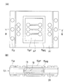
図17は、本発明の実施の形態2に係るフレキシブルリジッド多層プリント配線板の実際のレイアウト例を示す平面図である。 FIG. 17 is a plan view showing an actual layout example of the flexible rigid multilayer printed wiring board according to Embodiment 2 of the present invention.
本実施の形態に係るフレキシブルリジッド多層プリント配線板は、第2層導体パターン45のレイアウトとして、部品を実装するための部品実装端子45ptを形成してある。なお、中央部の2点鎖線で示した範囲が図2ないし図16で示した領域に対応する。フレキシブルリジッド多層プリント配線板は、リジッド領域Ar1およびリジッド領域Ar2をフレキシブル領域Afで接続したフォールディング仕様としてある。
The flexible rigid multilayer printed wiring board according to the present embodiment has component mounting terminals 45pt for mounting components as the layout of the second
図18は、本発明の実施の形態2に係るフレキシブルリジッド多層プリント配線板を製造するときに適用するワーク例を示す平面図である。 FIG. 18 is a plan view showing an example of a workpiece applied when manufacturing a flexible rigid multilayer printed wiring board according to Embodiment 2 of the present invention.
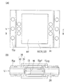
図17に示したフレキシブルリジッド多層プリント配線板は、ワーク60に複数個(例えば8個)配置され、同時に8個のフレキシブルリジッド多層プリント配線板を製造することが可能な構成としてある。
A plurality of (for example, eight) flexible rigid multilayer printed wiring boards shown in FIG. 17 are arranged on the
ワーク60は、例えば500mm×400mmの外形としてあり、位置合わせガイド61、ピンガイド(ピンラミネーションガイド)62が、例えば四隅に配置してある。位置合わせガイド61、ピンガイド(ピンラミネーションガイド)62を適用することにより、積層工程での位置合わせを容易かつ高精度に行なうことが可能となる。
The
<実施の形態3>
本発明に係るフレキシブルリジッド多層プリント配線板の第1層絶縁基材Liおよび第1層導体15の積層構造例を実施の形態3として図19ないし図25に基づいて説明する。なお、基本構成は実施の形態1、実施の形態2の場合と同様であるので重複する事項については適宜説明を省略する。
<Embodiment 3>
A laminated structure example of the first layer insulating base material Li and the
図19は、本発明の実施の形態3に係るフレキシブルリジッド多層プリント配線板の第1層絶縁基材および第1層導体の積層構造の実施例1を示す説明図であり、(A)は分解構成図、(B)は積層状態での断面の端面を示す端面図である。なお、断面の位置は実施の形態2で示した位置と同様の位置としてある(以下同様とする。)。 FIG. 19 is an explanatory view showing Example 1 of the laminated structure of the first layer insulating base material and the first layer conductor of the flexible rigid multilayer printed wiring board according to Embodiment 3 of the present invention, and (A) is an exploded view. A structure figure and (B) are end views showing an end face of a section in a lamination state. Note that the position of the cross section is the same as the position shown in the second embodiment (hereinafter the same).
可撓性を要求されるフレキシブル絶縁基材10を構成するフレキシブル絶縁フィルム10a、硬質性を要求されるリジッド絶縁基材20としてのガラス繊維強化エポキシ樹脂層20aを並置して第1層絶縁基材Liを構成する(第1層基材並置工程)。
A flexible
つまり、リジッド絶縁基材20に設けた開口部20wにフレキシブル絶縁基材10を嵌合する。この構成により、リジッド領域Arに対するフレキシブル領域Afの位置合わせを自己整合的に行なうことが可能となり、リジッド領域Arとフレキシブル領域Afの接合強度を向上させ信頼性を向上させることができる。
That is, the flexible insulating
次に、導体接着剤層16としての導体接着剤層16aを介して第1層絶縁基材Liに第1層導体15としての電解銅箔15aを積層(接着)する(第1層導体積層工程)。つまり、本実施例では、導体接着剤層16と第1層導体15をそれぞれ個別の部材である導体接着剤層16aと電解銅箔15aで構成する。なお、第1層導体15、導体接着剤層16を第1層絶縁基材Liの両面に対称的に配置することにより多層化することが可能である。
Next, the
リジッド領域Arとフレキシブル領域Afの間は、嵌合を自己整合的に容易に行なうために数μmから数十μm程度の空間を設けてあるが、積層(第1層導体積層工程)のときに導体接着剤層16(およびリジッド絶縁基材20が含有する接着剤)などが流動して充填されるので、リジッド領域Arおよびフレキシブル領域Afは相互に密着して結合され、十分な接続強度を持たせることが可能である。 A space of several μm to several tens of μm is provided between the rigid region Ar and the flexible region Af in order to facilitate fitting in a self-aligning manner, but at the time of lamination (first layer conductor lamination step) Since the conductive adhesive layer 16 (and the adhesive contained in the rigid insulating base material 20) flows and fills, the rigid region Ar and the flexible region Af are in close contact with each other and have sufficient connection strength. Is possible.
なお、フレキシブル絶縁フィルム10aは柔軟性を有する例えば厚さ50μmのポリイミドフィルム、ガラス繊維強化エポキシ樹脂層20aは例えば厚さ50μm、電解銅箔15aは例えば厚さ18μm、導体接着剤層16aは例えば厚さ50μmのエポキシ系樹脂接着剤層でそれぞれ構成してある。導体接着剤層16aはフレキシブル領域Afにも接着されることから、できるだけ柔軟性を有する構成とすることが望ましい。
The flexible
図20は、本発明の実施の形態3に係るフレキシブルリジッド多層プリント配線板の第1層絶縁基材および第1層導体の積層構造の実施例2を示す説明図であり、(A)は分解構成図、(B)は積層状態での断面の端面を示す端面図である。なお、主に実施例1と異なる事項について説明する。 FIG. 20 is an explanatory view showing Example 2 of the laminated structure of the first layer insulating base material and the first layer conductor of the flexible rigid multilayer printed wiring board according to Embodiment 3 of the present invention, and FIG. A structure figure and (B) are end views showing an end face of a section in a lamination state. Note that items different from the first embodiment will be mainly described.
本実施例では、実施例1で個別部材として積層した電解銅箔15aおよび導体接着剤層16aを予め接着したものとすることにより、第1層導体15としての電解銅箔15bおよび導体接着剤層16としての導体接着剤層16bが一体化されたものとしてある。
In this embodiment, the
つまり、第1層導体15(電解銅箔15b)のフレキシブル絶縁基材10およびリジッド絶縁基材20に対向する面に予め導体接着剤層16(導体接着剤層16b)が形成してある。この構成により、工程(第1層導体重畳工程、第1層導体積層工程)を簡略化することが可能となり、第1層導体15を確実かつ容易にフレキシブル絶縁基材10およびリジッド絶縁基材20に接着することができ、第1層絶縁基材Liでの接着強度を向上させて信頼性を向上させることが可能となる。
That is, the conductor adhesive layer 16 (
なお、電解銅箔15b(第1層導体15)および導体接着剤層16b(導体接着剤層16)を予め接着した部材は、一般に樹脂付き銅箔(RCC)として提供されるものを適用することができる。
In addition, as a member to which the
図21は、本発明の実施の形態3に係るフレキシブルリジッド多層プリント配線板の第1層絶縁基材および第1層導体の積層構造の実施例3を示す説明図であり、(A)は分解構成図、(B)は積層状態での断面の端面を示す端面図である。なお、実施例1、実施例2と異なる事項について主に説明する。 FIG. 21 is an explanatory view showing Example 3 of the laminated structure of the first layer insulating base material and the first layer conductor of the flexible rigid multilayer printed wiring board according to Embodiment 3 of the present invention, and (A) is an exploded view. A structure figure and (B) are end views showing an end face of a section in a lamination state. Items different from the first and second embodiments will be mainly described.
本実施例では、実施例2のガラス繊維強化エポキシ樹脂層20aを例えば厚さ50μmのプリプレグ(半硬化接着剤層)20bで置き換えてある。つまり、リジッド絶縁基材20は、半硬化接着剤層20bで構成してある。
In this example, the glass fiber reinforced
この構成により、リジッド領域Arでリジッド絶縁基材20と第1層導体15の接着を確実に行なうことができることから、リジッド領域Arの積層強度を向上させて信頼性を向上させることが可能となる。
With this configuration, since the rigid insulating
なお、半硬化接着剤層20bは、例えば、ガラス繊維強化エポキシ樹脂の半硬化接着剤層で構成することができる。
The semi-cured
図22は、本発明の実施の形態3に係るフレキシブルリジッド多層プリント配線板の第1層絶縁基材および第1層導体の積層構造の実施例4を示す説明図であり、(A)は分解構成図、(B)は積層状態での断面の端面を示す端面図である。なお、実施例1ないし実施例3と異なる事項について主に説明する。 FIG. 22 is an explanatory view showing Example 4 of the laminated structure of the first layer insulating base material and the first layer conductor of the flexible rigid multilayer printed wiring board according to Embodiment 3 of the present invention, and FIG. A structure figure and (B) are end views showing an end face of a section in a lamination state. Note that differences from the first to third embodiments will be mainly described.
本実施例では、実施例1ないし実施例3のフレキシブル絶縁フィルム10aを重畳した複数(例えば2枚)のフレキシブル絶縁フィルム11で置き換えてフレキシブル絶縁基材10を構成してある。
In this embodiment, the flexible insulating
フレキシブル絶縁フィルム11は、例えば厚さ25μmのポリイミドフィルムで構成することが可能であり、フレキシブル絶縁フィルム10aに比較してより薄いフレキシブル絶縁フィルム11を複数重畳して構成することから、フレキシブル領域Afの柔軟性および耐屈曲性を向上させることができる。
The flexible insulating
図23は、本発明の実施の形態3に係るフレキシブルリジッド多層プリント配線板の第1層絶縁基材および第1層導体の積層構造の実施例5を示す説明図であり、(A)は分解構成図、(B)は積層状態での断面の端面を示す端面図である。なお、実施例1ないし実施例4と異なる事項について主に説明する。 FIG. 23 is an explanatory view showing Example 5 of the laminated structure of the first layer insulating base material and the first layer conductor of the flexible rigid multilayer printed wiring board according to Embodiment 3 of the present invention, and FIG. A structure figure and (B) are end views showing an end face of a section in a lamination state. Note that differences from the first to fourth embodiments will be mainly described.
本実施例では、実施例4で適用したフレキシブル絶縁フィルム11の代わりに、第1層導体15に対向する表面に予め基材接着剤層12が塗布(形成)されたフレキシブル絶縁フィルム11aを適用してある。
In this example, instead of the flexible insulating
つまり、複数(2枚)のフレキシブル絶縁フィルム11aと最外側のフレキシブル絶縁フィルム11aに積層された基材接着剤層12でフレキシブル絶縁基材10を構成することとなる。この構成により、第1層導体15を最外側のフレキシブル絶縁フィルム11aに確実に接着できることから、高精度の第1層導体パターン15pを形成することが可能となる。
That is, the flexible insulating
フレキシブル絶縁フィルム11aは例えば厚さ20μmのポリイミドフィルムで構成され、基材接着剤層12は例えば厚さ15μmのエポキシ系樹脂接着剤層で構成してある。なお、フレキシブル絶縁フィルム11aおよび基材接着剤層12の構成は、いわゆるフィルムカバーレイを適用することが可能である。
The flexible
複数のフレキシブル絶縁フィルム11aおよびフレキシブル絶縁フィルム11aの最外側に積層した基材接着剤層12でフレキシブル絶縁基材10を構成することから、フレキシブル絶縁フィルム11a(厚さ20μm×2)および基材接着剤層12(厚さ15μm×2)の合計層厚(40μm+30μm=70μm)をリジッド絶縁基材20bの層厚(50μm)より厚く調整することが容易にできる。
Since the flexible insulating
この構成により、フレキシブル絶縁基材10およびリジッド絶縁基材20(半硬化接着剤層20b)に対向する面で第1層導体15(電解銅箔15b)に積層された導体接着剤層16(導体接着剤層16b)を第1層導体積層工程で押し出して薄膜化することができることから、フレキシブル領域Afの可撓性を確実に向上させることが可能となる。
With this configuration, the conductor adhesive layer 16 (conductor) laminated on the first layer conductor 15 (
また、積層するとき(第1層導体積層工程)の圧力は、リジッド領域Arよりフレキシブル領域Afの方が高くなり、接着剤(導体接着剤層16(導体接着剤層16b))がフレキシブル領域Afに侵入することを抑制することができる。
Moreover, the pressure at the time of laminating (first layer conductor laminating step) is higher in the flexible region Af than in the rigid region Ar, and the adhesive (conductor adhesive layer 16 (
図24は、本発明の実施の形態3に係るフレキシブルリジッド多層プリント配線板の第1層絶縁基材および第1層導体の積層構造の実施例6を示す説明図であり、(A)は分解構成図、(B)は積層状態での断面の端面を示す端面図である。なお、実施例1ないし実施例5と異なる事項について主に説明する。 FIG. 24 is an explanatory view showing Example 6 of the laminated structure of the first layer insulating base material and the first layer conductor of the flexible rigid multilayer printed wiring board according to Embodiment 3 of the present invention, and FIG. A structure figure and (B) are end views showing an end face of a section in a lamination state. Note that differences from the first to fifth embodiments will be mainly described.
本実施例では、実施例5で示した複数のフレキシブル絶縁フィルム11aの相互に対向する面の外周部を接着剤13で予め接着してある。接着剤13は、例えば厚さ4μmのエポキシ系樹脂接着剤層で構成することが可能である。接着剤13によるフレキシブル絶縁フィルム11aの相互接着は、第1層導体積層工程の前に予め行なうことが望ましい。
In the present embodiment, the outer peripheral portions of the mutually opposing surfaces of the plurality of flexible insulating
この構成により、プリプレグ(半硬化接着剤層20b)や樹脂付き銅箔(電解銅箔15bおよび導体接着剤層16b)の樹脂(接着剤)がフレキシブル絶縁基材10(フレキシブル絶縁フィルム11aの間)に侵入することを防止することができる。つまり、リジッド絶縁基材20側または第1層導体15側から流動してくる接着剤が相互に重畳したフレキシブル絶縁フィルム11aの間に侵入することを防止できるので、フレキシブル領域Afの可撓性および耐屈曲性を確実に維持することが可能となる。
With this configuration, the resin (adhesive) of the prepreg (semi-cured
図25は、本発明の実施の形態3に係るフレキシブルリジッド多層プリント配線板の第1層絶縁基材および第1層導体の積層構造の実施例7を示す説明図であり、(A)は分解構成図、(B)は積層状態での断面の端面を示す端面図である。なお、実施例1ないし実施例6と異なる事項について主に説明する。 FIG. 25 is an explanatory view showing Example 7 of the laminated structure of the first layer insulating base material and the first layer conductor of the flexible rigid multilayer printed wiring board according to Embodiment 3 of the present invention, and FIG. A structure figure and (B) are end views showing an end face of a section in a lamination state. Note that differences from the first to sixth embodiments will be mainly described.
また、積層状態(同図B)でリジッド領域Arおよびフレキシブル領域Afの間に空間を示しているが、この空間は実施例1ないし実施例6と同様に第1導体積層工程で周囲の接着剤が流動して充填される。図25では、構成部材を明確にするために接着剤の流動による充填状態は図示を省略する。 In addition, although a space is shown between the rigid region Ar and the flexible region Af in the laminated state (B in the same figure), this space is the surrounding adhesive in the first conductor laminating step as in the first to sixth embodiments. Fluidly fills. In FIG. 25, in order to clarify the constituent members, the filling state by the flow of the adhesive is not shown.
本実施例では、実施例2ないし実施例6で示した電解銅箔15b(第1層導体15)の構成を変更したものであり、リジッド領域Arおよびフレキシブル領域Afそれぞれに対応させて第1層導体15を分割してある。
In the present embodiment, the configuration of the
つまり、リジッド領域Arに配置された第1層導体15(電解銅箔15b)のリジッド絶縁基材20に対向する面に実施例2ないし実施例6と同様に予め導体接着剤層16bを形成してあり、フレキシブル領域Afに配置された第1層導体15(圧延銅箔15c)のフレキシブル絶縁基材10に対向する面には導体接着剤層16(導体接着剤層16b)を形成してない構成としてある。
That is, the
したがって、第1層導体15(圧延銅箔15c)のフレキシブル絶縁基材10に対向する面では導体接着剤層16bを除去してあり、フレキシブル領域Afを薄型化し接着剤(導体接着剤層16b)による影響を除去することができることから、フレキシブル領域Afの可撓性および耐屈曲性を向上することが可能となる。つまり、フレキシブル領域Afに配置された第1層導体15(圧延銅箔15c)は、フレキシブル絶縁基材10(基材接着剤層12)に直接積層される構成としてある。
Therefore, the
また、フレキシブル領域Afに対応する領域の第1層導体15は例えば厚さ18μmの圧延銅箔15cで構成してあり、リジッド領域Arに対応する領域の第1層導体15は電解銅箔15bで構成してある。一般に銅箔の屈曲性は電解銅箔に比較して圧延銅箔の方が大きい。つまり、第1層導体15は銅箔で構成してあり、フレキシブル絶縁基材10に対向する領域の銅箔(圧延銅箔15c)はリジッド絶縁基材20に対向する領域の銅箔(電解銅箔15b)より屈曲性が大きくしてある。
Further, the
したがって、フレキシブル領域Afの第1層導体15(圧延銅箔15c)の可撓性をリジッド領域Arの第1層導体15(電解銅箔15b)の可撓性に比較して大きくできるので、フレキシブル領域Af(フレキシブルリジッド多層プリント配線板)の耐屈曲性、信頼性を向上させることが可能となる。
Therefore, the flexibility of the first layer conductor 15 (rolled
また、例えば厚さ20μmのポリイミドフィルムで構成したフレキシブル絶縁フィルム11aおよび例えば厚さ15μmのエポキシ系樹脂接着剤層で構成した基材接着剤層12の合計層厚(70μm)を調整して例えば厚さ50μmの半硬化接着剤層20b(リジッド絶縁基材20)との段差を解消する構成とすることが、第1層導体パターンを高精度に歩留まり良く形成する(第1層パターン形成工程)ために望ましい。また、段差の解消は、半硬化接着剤層20bまたは導体接着剤層16bの厚さを調整して行なうことも可能である。
Further, for example, the total thickness (70 μm) of the flexible
<実施の形態4>
本実施の形態に係る電子機器(不図示)は、例えば2つのリジッド領域Arをフレキシブル領域Afで接続したフォールディング仕様のフレキシブルリジッド多層プリント配線板(図17参照。)に部品を実装して搭載することにより、筐体内での部品実装密度を向上させた電子機器としてある。
<Embodiment 4>
The electronic apparatus (not shown) according to the present embodiment mounts and mounts components on a flexible rigid multilayer printed wiring board (see FIG. 17) having a folding specification in which, for example, two rigid regions Ar are connected by a flexible region Af. Thus, the electronic device has an improved component mounting density in the housing.
つまり、本実施の形態に係る電子機器は、フレキシブルリジッド多層プリント配線板を搭載した電子機器であって、フレキシブルリジッド多層プリント配線板は、実施の形態1ないし実施の形態3で開示したフレキシブルリジッド多層プリント配線板としてある。 That is, the electronic device according to the present embodiment is an electronic device equipped with a flexible rigid multilayer printed wiring board, and the flexible rigid multilayer printed wiring board is the flexible rigid multilayer printed circuit disclosed in the first to third embodiments. As a printed wiring board.
この構成により、フレキシブル領域Af、リジッド領域Ar相互間の接続強度およびフレキシブル領域Afの耐屈曲性が大きく、接続信頼性の高い高品質の電子機器とすることが可能となる。 With this configuration, the connection strength between the flexible region Af and the rigid region Ar and the bending resistance of the flexible region Af are large, and a high-quality electronic device with high connection reliability can be provided.
10 フレキシブル絶縁基材
10a、11、11a フレキシブル絶縁フィルム(フレキシブル絶縁基材)
12 基材接着剤層
13 接着剤
15 第1層導体
15a、15b 電解銅箔(第1層導体)
15c 圧延銅箔(第1層導体)
15p 第1層導体パターン
15pf フレキシブルリードパターン
15pg 帯状保護パターン
16、16a、16b 導体接着剤層
20 リジッド絶縁基材
20a ガラス繊維強化エポキシ樹脂層(リジッド絶縁基材)
20b 半硬化接着剤層(リジッド絶縁基材)
20w 開口部
30 保護絶縁層
31 保護フィルム
32 保護接着剤
40 第2層絶縁基材
41 第2層導体
42 開口部
43 導通孔
44 導通孔導体
45 第2層導体パターン
50 ソルダーレジスト
50w 開口部
60 ワーク
Af フレキシブル領域
Aff 外形端部(フレキシブル領域)
Ar、Ar1、Ar2 リジッド領域
Arf 外形端部(リジッド領域外形)
Li 第1層絶縁基材
10 Flexible Insulating
12
15c Rolled copper foil (first layer conductor)
15p First layer conductor pattern 15pf Flexible lead pattern 15pg Band-shaped
20b Semi-cured adhesive layer (rigid insulating base)
20w opening 30 protective insulating
Ar, Ar1, Ar2 Rigid area Arf Outline end (rigid area outline)
Li first layer insulating substrate
Claims (18)
第1層絶縁基材として並置された可撓性を有するフレキシブル絶縁基材および硬質性を有するリジッド絶縁基材と、
前記第1層絶縁基材に積層された第1層導体と、
前記リジッド絶縁基材に積層された第2層絶縁基材および第2層導体とを備え、
前記フレキシブル絶縁基材は、重畳された複数のフレキシブル絶縁フィルムで構成してあることを特徴とするフレキシブルリジッド多層プリント配線板。 A flexible rigid multilayer printed wiring board comprising a flexible region having flexibility and a rigid region having rigidity,
A flexible insulating base material having flexibility and a rigid insulating base material having rigidity, juxtaposed as the first layer insulating base material;
A first layer conductor laminated on the first layer insulating substrate;
A second layer insulating base material and a second layer conductor laminated on the rigid insulating base material,
The flexible insulating multilayer printed wiring board, wherein the flexible insulating substrate is composed of a plurality of superimposed flexible insulating films.
可撓性を有するフレキシブル絶縁基材および硬質性を有するリジッド絶縁基材を第1層絶縁基材として並置する第1層基材並置工程と、
第1層絶縁基材に第1層導体を積層する第1層導体積層工程と、
前記第1層導体をパターニングして第1層導体パターンを形成する第1層パターン形成工程と、
前記リジッド絶縁基材に第2層絶縁基材および第2層導体を積層する第2層積層工程と
を備えることを特徴とするフレキシブルリジッド多層プリント配線板の製造方法。 A flexible rigid multilayer printed wiring board comprising a flexible region having flexibility and a rigid region having rigidity, comprising:
A first layer base material juxtaposition step of juxtaposing a flexible insulating base material having flexibility and a rigid insulating base material having rigidity as a first layer insulating base material;
A first layer conductor laminating step of laminating a first layer conductor on the first layer insulating substrate;
A first layer pattern forming step of patterning the first layer conductor to form a first layer conductor pattern;
And a second layer laminating step of laminating a second layer insulating base material and a second layer conductor on the rigid insulating base material. A method for producing a flexible rigid multilayer printed wiring board.
Priority Applications (1)
| Application Number | Priority Date | Filing Date | Title |
|---|---|---|---|
| JP2006350473A JP2008166300A (en) | 2006-12-26 | 2006-12-26 | Flexible rigid multilayer printed wiring board, method for manufacturing the same, and electronic device |
Applications Claiming Priority (1)
| Application Number | Priority Date | Filing Date | Title |
|---|---|---|---|
| JP2006350473A JP2008166300A (en) | 2006-12-26 | 2006-12-26 | Flexible rigid multilayer printed wiring board, method for manufacturing the same, and electronic device |
Publications (1)
| Publication Number | Publication Date |
|---|---|
| JP2008166300A true JP2008166300A (en) | 2008-07-17 |
Family
ID=39695437
Family Applications (1)
| Application Number | Title | Priority Date | Filing Date |
|---|---|---|---|
| JP2006350473A Pending JP2008166300A (en) | 2006-12-26 | 2006-12-26 | Flexible rigid multilayer printed wiring board, method for manufacturing the same, and electronic device |
Country Status (1)
| Country | Link |
|---|---|
| JP (1) | JP2008166300A (en) |
Cited By (2)
| Publication number | Priority date | Publication date | Assignee | Title |
|---|---|---|---|---|
| CN107799489A (en) * | 2016-09-05 | 2018-03-13 | 瑞萨电子株式会社 | Electronic installation |
| CN114025470A (en) * | 2017-11-01 | 2022-02-08 | 健鼎(无锡)电子有限公司 | Soft and hard composite circuit board and manufacturing method thereof |
-
2006
- 2006-12-26 JP JP2006350473A patent/JP2008166300A/en active Pending
Cited By (4)
| Publication number | Priority date | Publication date | Assignee | Title |
|---|---|---|---|---|
| CN107799489A (en) * | 2016-09-05 | 2018-03-13 | 瑞萨电子株式会社 | Electronic installation |
| CN107799489B (en) * | 2016-09-05 | 2022-10-25 | 瑞萨电子株式会社 | Electronic device |
| CN114025470A (en) * | 2017-11-01 | 2022-02-08 | 健鼎(无锡)电子有限公司 | Soft and hard composite circuit board and manufacturing method thereof |
| CN114025470B (en) * | 2017-11-01 | 2024-05-10 | 健鼎(无锡)电子有限公司 | Soft-hard composite circuit board and manufacturing method thereof |
Similar Documents
| Publication | Publication Date | Title |
|---|---|---|
| CN105722342B (en) | Flexible printed circuit board and manufacturing method thereof | |
| US7286370B2 (en) | Wired circuit board and connection structure of wired circuit board | |
| US9713267B2 (en) | Method for manufacturing printed wiring board with conductive post and printed wiring board with conductive post | |
| TW201410097A (en) | Multilayer flexible printed circuit board and method for manufacturing same | |
| TWI479972B (en) | Multi-layer flexible printed wiring board and manufacturing method thereof | |
| KR101980102B1 (en) | Method for Manufacturing Rigid-Flexible PCB | |
| JP4768059B2 (en) | Multilayer flexible printed wiring board | |
| KR20100127253A (en) | Manufacturing method of rigid flex circuit board and rigid flex circuit board | |
| JP5464760B2 (en) | Multilayer circuit board manufacturing method | |
| US20150040389A1 (en) | Method for manufacturing wiring board with built-in electronic component | |
| US9743511B1 (en) | Rigid flex circuit board | |
| KR101946989B1 (en) | The printed circuit board and the method for manufacturing the same | |
| JP5524315B2 (en) | Display element module using multilayer flexible printed wiring board | |
| EP2007179B1 (en) | Multilayer circuit board having cable portion and method for manufacturing same | |
| US7685707B2 (en) | Method for manufacturing circuit forming substrate | |
| JP2008300658A (en) | Flexible rigid multilayer printed wiring board and method for manufacturing the same | |
| CN107889356B (en) | Soft and hard composite circuit board | |
| JP2008166300A (en) | Flexible rigid multilayer printed wiring board, method for manufacturing the same, and electronic device | |
| JP2009021425A (en) | Flexible rigid printed circuit board, flexible rigid printed circuit board manufacturing method, and electronic apparatus | |
| CN114258200B (en) | Manufacturing method of soft and hard combined circuit board with embedded element | |
| JP6387226B2 (en) | Composite board | |
| JP4850084B2 (en) | Electric wire composite printed wiring board, electric wire composite printed wiring board manufacturing method, electric wire component, electric wire component manufacturing method, and electronic device | |
| KR100665244B1 (en) | Circuit wiring composite board | |
| KR20160139829A (en) | Multilayer fpcb and fabricating method thereof | |
| KR101390696B1 (en) | Printed circuit board and method of manufacturing thereof |