JP2008134639A - 半導体装置 - Google Patents
半導体装置 Download PDFInfo
- Publication number
- JP2008134639A JP2008134639A JP2007310135A JP2007310135A JP2008134639A JP 2008134639 A JP2008134639 A JP 2008134639A JP 2007310135 A JP2007310135 A JP 2007310135A JP 2007310135 A JP2007310135 A JP 2007310135A JP 2008134639 A JP2008134639 A JP 2008134639A
- Authority
- JP
- Japan
- Prior art keywords
- light receiving
- elements
- light emitting
- integrated circuit
- semiconductor device
- Prior art date
- Legal status (The legal status is an assumption and is not a legal conclusion. Google has not performed a legal analysis and makes no representation as to the accuracy of the status listed.)
- Pending
Links
- 239000004065 semiconductor Substances 0.000 title claims abstract description 93
- 230000003287 optical effect Effects 0.000 claims abstract description 162
- 230000005693 optoelectronics Effects 0.000 claims abstract description 66
- 239000000758 substrate Substances 0.000 claims abstract description 63
- 238000009429 electrical wiring Methods 0.000 description 12
- 238000000034 method Methods 0.000 description 12
- 239000004020 conductor Substances 0.000 description 9
- 230000005540 biological transmission Effects 0.000 description 8
- 238000004519 manufacturing process Methods 0.000 description 7
- 230000000694 effects Effects 0.000 description 6
- 239000000463 material Substances 0.000 description 6
- 238000000206 photolithography Methods 0.000 description 6
- 229910052782 aluminium Inorganic materials 0.000 description 5
- XAGFODPZIPBFFR-UHFFFAOYSA-N aluminium Chemical compound [Al] XAGFODPZIPBFFR-UHFFFAOYSA-N 0.000 description 5
- 238000005253 cladding Methods 0.000 description 5
- 239000010410 layer Substances 0.000 description 5
- 238000004528 spin coating Methods 0.000 description 5
- 239000012792 core layer Substances 0.000 description 4
- KPUWHANPEXNPJT-UHFFFAOYSA-N disiloxane Chemical class [SiH3]O[SiH3] KPUWHANPEXNPJT-UHFFFAOYSA-N 0.000 description 4
- 238000005516 engineering process Methods 0.000 description 4
- 229920000642 polymer Polymers 0.000 description 4
- 230000008054 signal transmission Effects 0.000 description 4
- 239000004642 Polyimide Substances 0.000 description 3
- 230000008878 coupling Effects 0.000 description 3
- 238000010168 coupling process Methods 0.000 description 3
- 238000005859 coupling reaction Methods 0.000 description 3
- 238000010438 heat treatment Methods 0.000 description 3
- 238000005259 measurement Methods 0.000 description 3
- 229920001721 polyimide Polymers 0.000 description 3
- 238000012545 processing Methods 0.000 description 3
- PNEYBMLMFCGWSK-UHFFFAOYSA-N aluminium oxide Inorganic materials [O-2].[O-2].[O-2].[Al+3].[Al+3] PNEYBMLMFCGWSK-UHFFFAOYSA-N 0.000 description 2
- UMIVXZPTRXBADB-UHFFFAOYSA-N benzocyclobutene Chemical compound C1=CC=C2CCC2=C1 UMIVXZPTRXBADB-UHFFFAOYSA-N 0.000 description 2
- 239000011521 glass Substances 0.000 description 2
- 230000010354 integration Effects 0.000 description 2
- 229910052751 metal Inorganic materials 0.000 description 2
- 239000002184 metal Substances 0.000 description 2
- 239000003960 organic solvent Substances 0.000 description 2
- 238000001020 plasma etching Methods 0.000 description 2
- 229920003229 poly(methyl methacrylate) Polymers 0.000 description 2
- 239000004926 polymethyl methacrylate Substances 0.000 description 2
- 239000000243 solution Substances 0.000 description 2
- 238000004544 sputter deposition Methods 0.000 description 2
- NIXOWILDQLNWCW-UHFFFAOYSA-M Acrylate Chemical compound [O-]C(=O)C=C NIXOWILDQLNWCW-UHFFFAOYSA-M 0.000 description 1
- YCKRFDGAMUMZLT-UHFFFAOYSA-N Fluorine atom Chemical compound [F] YCKRFDGAMUMZLT-UHFFFAOYSA-N 0.000 description 1
- 239000004697 Polyetherimide Substances 0.000 description 1
- 239000004793 Polystyrene Substances 0.000 description 1
- XUIMIQQOPSSXEZ-UHFFFAOYSA-N Silicon Chemical compound [Si] XUIMIQQOPSSXEZ-UHFFFAOYSA-N 0.000 description 1
- 150000001252 acrylic acid derivatives Chemical class 0.000 description 1
- 238000003491 array Methods 0.000 description 1
- FPCJKVGGYOAWIZ-UHFFFAOYSA-N butan-1-ol;titanium Chemical compound [Ti].CCCCO.CCCCO.CCCCO.CCCCO FPCJKVGGYOAWIZ-UHFFFAOYSA-N 0.000 description 1
- 238000006243 chemical reaction Methods 0.000 description 1
- 238000004891 communication Methods 0.000 description 1
- 230000006866 deterioration Effects 0.000 description 1
- 238000010586 diagram Methods 0.000 description 1
- 238000009792 diffusion process Methods 0.000 description 1
- KZHJGOXRZJKJNY-UHFFFAOYSA-N dioxosilane;oxo(oxoalumanyloxy)alumane Chemical compound O=[Si]=O.O=[Si]=O.O=[Al]O[Al]=O.O=[Al]O[Al]=O.O=[Al]O[Al]=O KZHJGOXRZJKJNY-UHFFFAOYSA-N 0.000 description 1
- 238000006073 displacement reaction Methods 0.000 description 1
- 238000001312 dry etching Methods 0.000 description 1
- 238000005530 etching Methods 0.000 description 1
- 229910052731 fluorine Inorganic materials 0.000 description 1
- 239000011737 fluorine Substances 0.000 description 1
- 238000007429 general method Methods 0.000 description 1
- 239000002241 glass-ceramic Substances 0.000 description 1
- 238000005342 ion exchange Methods 0.000 description 1
- 238000005468 ion implantation Methods 0.000 description 1
- 239000011259 mixed solution Substances 0.000 description 1
- 229910052863 mullite Inorganic materials 0.000 description 1
- 229920002120 photoresistant polymer Polymers 0.000 description 1
- 229920000548 poly(silane) polymer Polymers 0.000 description 1
- 239000004417 polycarbonate Substances 0.000 description 1
- 229920000515 polycarbonate Polymers 0.000 description 1
- 229920001601 polyetherimide Polymers 0.000 description 1
- 238000006116 polymerization reaction Methods 0.000 description 1
- 229920001296 polysiloxane Polymers 0.000 description 1
- 229920002223 polystyrene Polymers 0.000 description 1
- 238000007639 printing Methods 0.000 description 1
- 230000002250 progressing effect Effects 0.000 description 1
- 239000010453 quartz Substances 0.000 description 1
- 238000011160 research Methods 0.000 description 1
- 239000011347 resin Substances 0.000 description 1
- 229920005989 resin Polymers 0.000 description 1
- 230000000630 rising effect Effects 0.000 description 1
- 230000035945 sensitivity Effects 0.000 description 1
- 229910052710 silicon Inorganic materials 0.000 description 1
- 239000010703 silicon Substances 0.000 description 1
- VYPSYNLAJGMNEJ-UHFFFAOYSA-N silicon dioxide Inorganic materials O=[Si]=O VYPSYNLAJGMNEJ-UHFFFAOYSA-N 0.000 description 1
- 238000002207 thermal evaporation Methods 0.000 description 1
- 238000001039 wet etching Methods 0.000 description 1
Images


Landscapes
- Optical Couplings Of Light Guides (AREA)
- Light Receiving Elements (AREA)
Abstract
【解決手段】 支持基板1上に、電子集積回路素子9ならびに複数個の受光素子5および発光素子4が同一基板上に設けられた光電子集積回路素子2が複数個配置されるとともに、光電子集積回路素子9間で受光素子5と発光素子4とを接続する複数本の光導波路6が形成されて成り、隣接するこれら光導波路6における光の伝搬方向が逆方向とされている半導体装置である。また、隣接する光導波路6に接続された受光素子5および発光素子4は、交互に位置をずらせて配置するとよく、さらにそれぞれ複数個が一体的にアレイ状に形成されているとよい。隣接する光導波路6間のクロストークを低減でき、低コストおよび損失のより小さな半導体装置を提供することができる。
【選択図】 図1
Description
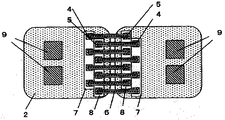
半導体レーザ(LD)等が該当する。また、受光素子5については、pin型フォトダイオード・アバランシェフォトダイオード(APD)・MSM型フォトダイオード等が該当する。そして、これら発光素子4および受光素子5は、それぞれの光電子集積回路素子2において、隣接する光導波路6について交互に配置されており、これにより隣接する光導波路6における光の伝搬方向が逆方向とされている。
ており、隣接する光導波路6における光の伝搬方向が逆方向とされている。
まず、支持基板となるアルミナ基板の表面に、シロキサンポリマの有機溶媒溶液をスピンコート法によって塗布し、85℃/30分および270℃/30分の熱処理を行ない、厚さ8μmの下部クラッド層(屈折率1.4405,λ=1.3μm)を形成した。
[実施例1]と同様にして本発明の半導体装置を作製するのに際して、受光素子としてMSM型フォトダイオードを、発光素子として半導体レーザを、それぞれ真空プロセスおよびフォトリソグラフィプロセスにて形成し、光電子集積回路素子にその並びが交互に、また発光素子と受光素子との位置を20μmずらせたものとなるように配置した。
[実施例1]と同様にして本発明の半導体装置を作製するのに際して、受光素子としてMSM型フォトダイオードを、発光素子として半導体レーザを、それぞれ真空プロセスおよびフォトリソグラフィプロセスにて形成し、光電子集積回路素子に、受光素子および発光素子がそれぞれ40μm間隔で一体的にアレイ状に形成されて、その並びが交互に、また発光素子と受光素子との位置を20μmずらせたものとなるように配置した。
2 光電子集積回路素子
3 導体バンプ
4 発光素子
5 受光素子
6 光導波路
7 発光素子アレイ
8 受光素子アレイ
9 電子集積回路素子
Claims (3)
- 支持基板上に、電子集積回路素子ならびに複数個の受光素子および発光素子が同一基板上に設けられた光電子集積回路素子が複数個配置されるとともに、前記光電子集積回路素子間で前記受光素子と前記発光素子とを接続する複数本の光導波路が形成されて成り、隣接するこれら光導波路における光の伝搬方向が逆方向とされていることを特徴とする半導体装置。
- 隣接する前記光導波路により接続された前記受光素子および前記発光素子が、前記光電子集積回路素子において隣接する前記光導波路について交互に位置をずらせて配置されていることを特徴とする請求項1記載の半導体装置。
- 交互に位置をずらせて配置された前記受光素子および前記発光素子が、前記光電子集積回路素子においてそれぞれ複数個が一体的にアレイ状に形成されていることを特徴とする請求項2記載の半導体装置。
Priority Applications (1)
| Application Number | Priority Date | Filing Date | Title |
|---|---|---|---|
| JP2007310135A JP2008134639A (ja) | 2007-11-30 | 2007-11-30 | 半導体装置 |
Applications Claiming Priority (1)
| Application Number | Priority Date | Filing Date | Title |
|---|---|---|---|
| JP2007310135A JP2008134639A (ja) | 2007-11-30 | 2007-11-30 | 半導体装置 |
Related Parent Applications (1)
| Application Number | Title | Priority Date | Filing Date |
|---|---|---|---|
| JP2002019022A Division JP4646479B2 (ja) | 2002-01-28 | 2002-01-28 | 半導体装置 |
Publications (2)
| Publication Number | Publication Date |
|---|---|
| JP2008134639A true JP2008134639A (ja) | 2008-06-12 |
| JP2008134639A5 JP2008134639A5 (ja) | 2009-03-12 |
Family
ID=39559481
Family Applications (1)
| Application Number | Title | Priority Date | Filing Date |
|---|---|---|---|
| JP2007310135A Pending JP2008134639A (ja) | 2007-11-30 | 2007-11-30 | 半導体装置 |
Country Status (1)
| Country | Link |
|---|---|
| JP (1) | JP2008134639A (ja) |
Citations (5)
| Publication number | Priority date | Publication date | Assignee | Title |
|---|---|---|---|---|
| JP2000082807A (ja) * | 1998-09-04 | 2000-03-21 | Seiko Epson Corp | 光伝達手段を備えた装置 |
| WO2000036448A1 (en) * | 1998-12-15 | 2000-06-22 | Telefonaktiebolaget Lm Ericsson (Publ) | An optical transmitter-receiver module |
| JP2000227825A (ja) * | 1998-12-03 | 2000-08-15 | Nippon Telegr & Teleph Corp <Ntt> | 高速信号処理装置 |
| JP2000269586A (ja) * | 1999-03-16 | 2000-09-29 | Fuji Xerox Co Ltd | 光送受信モジュールの製造方法 |
| JP2003224293A (ja) * | 2002-01-28 | 2003-08-08 | Kyocera Corp | 半導体装置 |
-
2007
- 2007-11-30 JP JP2007310135A patent/JP2008134639A/ja active Pending
Patent Citations (5)
| Publication number | Priority date | Publication date | Assignee | Title |
|---|---|---|---|---|
| JP2000082807A (ja) * | 1998-09-04 | 2000-03-21 | Seiko Epson Corp | 光伝達手段を備えた装置 |
| JP2000227825A (ja) * | 1998-12-03 | 2000-08-15 | Nippon Telegr & Teleph Corp <Ntt> | 高速信号処理装置 |
| WO2000036448A1 (en) * | 1998-12-15 | 2000-06-22 | Telefonaktiebolaget Lm Ericsson (Publ) | An optical transmitter-receiver module |
| JP2000269586A (ja) * | 1999-03-16 | 2000-09-29 | Fuji Xerox Co Ltd | 光送受信モジュールの製造方法 |
| JP2003224293A (ja) * | 2002-01-28 | 2003-08-08 | Kyocera Corp | 半導体装置 |
Similar Documents
| Publication | Publication Date | Title |
|---|---|---|
| US11424837B2 (en) | Method and system for large silicon photonic interposers by stitching | |
| US6684007B2 (en) | Optical coupling structures and the fabrication processes | |
| US6706546B2 (en) | Optical reflective structures and method for making | |
| US6785447B2 (en) | Single and multilayer waveguides and fabrication process | |
| US6690845B1 (en) | Three-dimensional opto-electronic modules with electrical and optical interconnections and methods for making | |
| US10168474B2 (en) | Method of manufacturing optical input/output device | |
| US6845184B1 (en) | Multi-layer opto-electronic substrates with electrical and optical interconnections and methods for making | |
| US6963119B2 (en) | Integrated optical transducer assembly | |
| US6611635B1 (en) | Opto-electronic substrates with electrical and optical interconnections and methods for making | |
| US6343171B1 (en) | Systems based on opto-electronic substrates with electrical and optical interconnections and methods for making | |
| US7923273B2 (en) | Stackable optoelectronics chip-to-chip interconnects and method of manufacturing | |
| JP5445579B2 (ja) | 光導波路モジュール | |
| US8437584B2 (en) | Optical I/O array module and its fabrication method | |
| KR100993385B1 (ko) | 광학적 상호접속부를 구비하는 장치, 프로세싱 시스템 및광학적 상호접속부 제조 방법 | |
| TWI376038B (ja) | ||
| US20100215313A1 (en) | Optical interconnection assembled circuit | |
| WO2018198490A1 (ja) | 光電子集積回路及びコンピューティング装置 | |
| US11966090B2 (en) | Heterogeneous packaging integration of photonic and electronic elements | |
| JP4243456B2 (ja) | 半導体装置 | |
| JP2008102283A (ja) | 光導波路、光モジュール及び光導波路の製造方法 | |
| JP4690870B2 (ja) | 光電気集積配線基板及び光電気集積配線システム | |
| JP4646479B2 (ja) | 半導体装置 | |
| JP4999813B2 (ja) | 半導体装置 | |
| JPH1152198A (ja) | 光接続構造 | |
| JP2006047894A (ja) | 光導波装置 |
Legal Events
| Date | Code | Title | Description |
|---|---|---|---|
| A521 | Request for written amendment filed |
Free format text: JAPANESE INTERMEDIATE CODE: A523 Effective date: 20090126 |
|
| A131 | Notification of reasons for refusal |
Free format text: JAPANESE INTERMEDIATE CODE: A131 Effective date: 20090707 |
|
| A131 | Notification of reasons for refusal |
Free format text: JAPANESE INTERMEDIATE CODE: A131 Effective date: 20100629 |
|
| A521 | Request for written amendment filed |
Free format text: JAPANESE INTERMEDIATE CODE: A523 Effective date: 20100830 |
|
| A02 | Decision of refusal |
Free format text: JAPANESE INTERMEDIATE CODE: A02 Effective date: 20101026 |