JP2008083679A - Display unit and electronic equipment - Google Patents
Display unit and electronic equipment Download PDFInfo
- Publication number
- JP2008083679A JP2008083679A JP2007164642A JP2007164642A JP2008083679A JP 2008083679 A JP2008083679 A JP 2008083679A JP 2007164642 A JP2007164642 A JP 2007164642A JP 2007164642 A JP2007164642 A JP 2007164642A JP 2008083679 A JP2008083679 A JP 2008083679A
- Authority
- JP
- Japan
- Prior art keywords
- display
- unit
- signal
- transmission
- substrate
- Prior art date
- Legal status (The legal status is an assumption and is not a legal conclusion. Google has not performed a legal analysis and makes no representation as to the accuracy of the status listed.)
- Withdrawn
Links
Images


Classifications
-
- G—PHYSICS
- G06—COMPUTING; CALCULATING OR COUNTING
- G06F—ELECTRIC DIGITAL DATA PROCESSING
- G06F1/00—Details not covered by groups G06F3/00 - G06F13/00 and G06F21/00
- G06F1/16—Constructional details or arrangements
- G06F1/1601—Constructional details related to the housing of computer displays, e.g. of CRT monitors, of flat displays
-
- G—PHYSICS
- G09—EDUCATION; CRYPTOGRAPHY; DISPLAY; ADVERTISING; SEALS
- G09G—ARRANGEMENTS OR CIRCUITS FOR CONTROL OF INDICATING DEVICES USING STATIC MEANS TO PRESENT VARIABLE INFORMATION
- G09G5/00—Control arrangements or circuits for visual indicators common to cathode-ray tube indicators and other visual indicators
- G09G5/003—Details of a display terminal, the details relating to the control arrangement of the display terminal and to the interfaces thereto
- G09G5/006—Details of the interface to the display terminal
-
- G—PHYSICS
- G09—EDUCATION; CRYPTOGRAPHY; DISPLAY; ADVERTISING; SEALS
- G09G—ARRANGEMENTS OR CIRCUITS FOR CONTROL OF INDICATING DEVICES USING STATIC MEANS TO PRESENT VARIABLE INFORMATION
- G09G2330/00—Aspects of power supply; Aspects of display protection and defect management
- G09G2330/08—Fault-tolerant or redundant circuits, or circuits in which repair of defects is prepared
-
- G—PHYSICS
- G09—EDUCATION; CRYPTOGRAPHY; DISPLAY; ADVERTISING; SEALS
- G09G—ARRANGEMENTS OR CIRCUITS FOR CONTROL OF INDICATING DEVICES USING STATIC MEANS TO PRESENT VARIABLE INFORMATION
- G09G2370/00—Aspects of data communication
- G09G2370/16—Use of wireless transmission of display information
-
- G—PHYSICS
- G09—EDUCATION; CRYPTOGRAPHY; DISPLAY; ADVERTISING; SEALS
- G09G—ARRANGEMENTS OR CIRCUITS FOR CONTROL OF INDICATING DEVICES USING STATIC MEANS TO PRESENT VARIABLE INFORMATION
- G09G3/00—Control arrangements or circuits, of interest only in connection with visual indicators other than cathode-ray tubes
- G09G3/20—Control arrangements or circuits, of interest only in connection with visual indicators other than cathode-ray tubes for presentation of an assembly of a number of characters, e.g. a page, by composing the assembly by combination of individual elements arranged in a matrix no fixed position being assigned to or needed to be assigned to the individual characters or partial characters
- G09G3/34—Control arrangements or circuits, of interest only in connection with visual indicators other than cathode-ray tubes for presentation of an assembly of a number of characters, e.g. a page, by composing the assembly by combination of individual elements arranged in a matrix no fixed position being assigned to or needed to be assigned to the individual characters or partial characters by control of light from an independent source
- G09G3/36—Control arrangements or circuits, of interest only in connection with visual indicators other than cathode-ray tubes for presentation of an assembly of a number of characters, e.g. a page, by composing the assembly by combination of individual elements arranged in a matrix no fixed position being assigned to or needed to be assigned to the individual characters or partial characters by control of light from an independent source using liquid crystals
- G09G3/3611—Control of matrices with row and column drivers
Abstract
Description
本発明は、例えば、携帯電話やノートブックコンピュータ、デジタルカメラの電子機器に適用される表示装置、および、該表示装置を適用した電子機器に関し、特に、この種の表示素子の実装技術に関する。 The present invention relates to, for example, a display device applied to an electronic device such as a mobile phone, a notebook computer, or a digital camera, and an electronic device to which the display device is applied, and more particularly to a mounting technology for this type of display element.
近年、携帯電話やノートブックコンピュータ、デジタルカメラなどの機能向上は目覚しく、これらの電子機器に内蔵される表示素子や撮像素子の高分解能化および高精細化が求められ、ますます複雑化してきている。特に携帯電話においては、カメラ機能の内蔵化や表示部の大型化などの高機能化とともに小型軽量化および低消費電力化が求められ、その筐体構造も、クラムシェル型またはフリップ型と呼ばれる折り畳み型が主流になってきている。
これらの表示体素子や撮像素子を内蔵する電子機器において、最近はますます表示部の大型化および高分解能化、更に電子機器の小型軽量化が求められてきている。このような要請から、実装基板は複数に分割実装されることが多い。
In recent years, functions of mobile phones, notebook computers, digital cameras, etc. have improved dramatically, and higher resolution and higher definition of display elements and imaging elements built into these electronic devices have become increasingly complex. . In particular, mobile phones are required to have high functionality such as built-in camera functions and large display units, as well as small size, light weight, and low power consumption, and the housing structure is also a clamshell type or flip type folding type. Molds are becoming mainstream.
In electronic devices incorporating these display elements and image sensors, recently, there has been an increasing demand for larger display sizes and higher resolutions, and for smaller and lighter electronic devices. Due to such demands, the mounting substrate is often divided and mounted in plural.
その場合に表示体は図12のように独立した機能として駆動回路などと一体化されたモジュール1201となり本体側とはコネクタ1203を介してケーブル1202によって接続される。ケーブル1202にはフレキシブル基板上に印刷されたフラットケーブルや細線同軸ケーブルが使用される。
素子の高分解能化に伴い、表示体(モジュール)側と本体側とを結ぶ線路の信号周波数が高くなりかつ信号のピン数も多くなってきており、接続が困難になってきている。電子機器の小型化の要請はコネクタを小さく作ることを要請しこれに伴ってコネクタの信頼性は低下している。
In that case, the display body becomes a
As the resolution of elements increases, the signal frequency of the line connecting the display body (module) side and the main body side increases, and the number of signal pins increases, making connection difficult. The demand for miniaturization of electronic devices requires that the connector be made smaller, and accordingly, the reliability of the connector is lowered.
現在、携帯電話などに用いられるこれらのコネクタは挿抜回数の保障限界は数回と極端に低い。
この問題を解決するためにデータ伝送を高速化してピン数を減らす試みがあり、高速データ伝送の方式として、たとえばLVDS(Low Voltage Differential Signaling)を表示体や撮像素子の接続に使う(特許文献1および特許文献2)ことが提案されている。
In order to solve this problem, there is an attempt to increase the speed of data transmission and reduce the number of pins. As a high-speed data transmission system, for example, LVDS (Low Voltage Differential Signaling) is used for connection of a display body or an image sensor (Patent Document 1). And Patent Document 2) have been proposed.
しかしながら、最近の表示体の大型化はこれらの技術でも十分な性能を得られない。即ち、LVDSのような小信号シリアル転送では、十分な対ノイズ特性(耐干渉性、与干渉性)を得るには細心の設計と調整が要求される。LVDSでは信号振幅が小さいため、必然的にデジタルICでアナログ信号を扱うことになり、消費電力が大きくなるという問題があった。 However, recent increases in the size of display bodies cannot provide sufficient performance even with these technologies. That is, in small signal serial transfer such as LVDS, careful design and adjustment are required to obtain sufficient anti-noise characteristics (interference immunity and interference). In LVDS, since the signal amplitude is small, an analog signal is inevitably handled by a digital IC, and there is a problem that power consumption increases.
また、信号を精度よく伝送するためには、整合の取れたインピーダンス終端が必要であるが、コネクタ部はケーブルや平行線による伝送線路のようにインピーダンス設計が容易でなく従来の技術では接続部において必ずミスマッチを起こす。またインピーダンス終端が必要とされる線の数が多い上に伝送インピーダンスはせいぜい100オーム程度であるため、それらの終端抵抗に消費される電力が容認できない程に大きくなってしまうという問題もあった。 In addition, in order to transmit signals with high accuracy, matched impedance termination is required. However, impedance design is not easy for connector parts like cables and transmission lines using parallel lines. Always make a mismatch. In addition, since the number of lines that require impedance termination is large and the transmission impedance is at most about 100 ohms, the power consumed by these termination resistors becomes unacceptably large.
また、上記のような高速データ伝送を用いても、信号数は十数本となり、コネクタを介してフレキシブル基板などで接続することになる。フレキシブル基板やコネクタによる接続はコストが高い上に、接続信頼性も低いという欠点を有していた。更に、配線のために必要な物理的スペースは、当然ながら電子機器のデザインに対し大きな制約を課すことになる。 Moreover, even if the high-speed data transmission as described above is used, the number of signals becomes ten and more, and they are connected by a flexible board or the like through a connector. Connections using flexible substrates and connectors have the disadvantages of high cost and low connection reliability. Furthermore, the physical space required for wiring naturally places significant constraints on the design of electronic equipment.
これらの問題は電子回路や集積回路の各ブロック間での信号の授受に従来の無線通信技術を導入し、配線が困難な部分のデータ転送を電磁波(電波)信号により無線で転送すれば一気に解決できるとして、非特許文献1や特許文献3乃至6に開示されている技術が注目される。
しかしながら、従来の無線通信技術を電子機器内のデータ転送に導入するには、その仕組みが、導線により伝送していた場合に比較し、非常に複雑であり実装には困難が伴う。
These problems can be solved all at once by introducing conventional wireless communication technology to send and receive signals between each block of electronic circuits and integrated circuits, and wirelessly transferring data in difficult-to-wiring portions using electromagnetic wave (radio wave) signals. As possible, the techniques disclosed in
However, in order to introduce the conventional wireless communication technology to data transfer in an electronic device, the mechanism is very complicated and difficult to implement compared to the case where transmission is performed by a conductive wire.
特に、電子機器内での接続のためのアンテナの配置が実装時において非常に困難な課題となる。特許文献3乃至6には、どれも有効な解決策が示されていない。たとえば特許文献4では、1.5GHzの電波を使用する四分の一波長のアンテナを集積回路上に集積すると開示されているが、1.5GHzの電波の波長は20cmであり、四分の一波長即ち5cmのアンテナを集積回路上に集積するのは明らかに不可能である。 In particular, the arrangement of antennas for connection within an electronic device is a very difficult problem during mounting. Patent documents 3 to 6 do not show any effective solutions. For example, Patent Document 4 discloses that a quarter-wavelength antenna using a 1.5 GHz radio wave is integrated on an integrated circuit, but the wavelength of the 1.5 GHz radio wave is 20 cm, which is a quarter. It is clearly impossible to integrate a wavelength or 5 cm antenna on an integrated circuit.
また特許文献5、6では、半導体チップ上に絶縁膜を形成し、その上に平面状のアンテナ放射器を置く構造が示されているが、半導体チップ上における絶縁膜程度の厚さでは、該絶縁膜上に置かれた放射器からは効率よく電磁波を放射させることができないことはこの種の技術分野における通常の知識を有する技術者にとって論を俟たずに理解されるところである。
一方、携帯電話等では機器本来の目的である遠方との通信のための送受信機を内蔵しておりこの送受信機への妨害や送受信機から受ける妨害排除も課題となる。従来の無線通信技術ではこのような機器内部の極近距離の無線通信でしかも極端に大きな電力の電波を発射する送信機が同一筺体内にあるような極端な環境での通信確保のための技術は提供されていない。
更に、以下のような課題もある。近年の半導体プロセスの進化によってその動作電圧が低下する傾向にある。従来TTL(Transistor- Transistor-Logic)レベルとしてICの電源電圧および信号振幅は5Vが永年にわたり使用されてきた。近年は電源電圧および信号の振幅に3.3Vが使用されるようになっている。
On the other hand, a mobile phone or the like has a built-in transmitter / receiver for communication with a distant place, which is the original purpose of the device, and there is also a problem of obstructing the transmitter / receiver and eliminating interference received from the transmitter / receiver. Conventional wireless communication technology is a technology for ensuring communication in an extreme environment where a transmitter that emits a radio wave of extremely large power is in the same housing within a short distance wireless communication inside the device. Is not provided.
Furthermore, there are the following problems. The operating voltage tends to decrease due to recent advances in semiconductor processes. Conventionally, as a TTL (Transistor-Transistor-Logic) level, an IC power supply voltage and signal amplitude of 5 V have been used for many years. In recent years, 3.3V has been used for power supply voltage and signal amplitude.
しかしながら近年の半導体プロセスの進化によって更に動作電圧が低下し1V程度まで下がりつつある。ここで問題となるのは複数のICを接続する場合のインターフェースの信号振幅レベルである。信号振幅レベルは3.3Vが標準として定着しているため、ICプロセスが進化したからといって設計者の任意で異なる信号振幅レベルを採用することは多数の標準を必要とするなど混乱が避けられない。
このような混乱を回避するため、現在の解決策としてはICの内部では各プロセスで最適な電源電圧で動作させ、その電源電圧レベルから3.3V系の標準の信号レベルに変換するインターフェース回路を各ICに内蔵させている。
However, with the recent progress of semiconductor processes, the operating voltage is further lowered to about 1V. The problem here is the signal amplitude level of the interface when a plurality of ICs are connected. Since the signal amplitude level is established as 3.3V as a standard, the adoption of arbitrarily different signal amplitude levels by the designer even if the IC process has evolved requires many standards and avoids confusion. I can't.
In order to avoid such confusion, the current solution is to operate an interface circuit that operates at the optimum power supply voltage in each process inside the IC and converts the power supply voltage level to a 3.3V standard signal level. Built in each IC.
ICプロセスが進化した現在では多くの場面で、すべてのICチップが内部では1V程度の低電圧で動作しているにもかかわらずそれらICチップ間を互いに接続するインターフェース部分ではわざわざ標準の信号レベルを確保するために3.3Vに変換する回路を付加している。
このことは変換回路の消費電力、動作速度の点からICの性能に制約を課し、またICの製造プロセスも内部回路の最適な動作電圧で動作する部分と3.3Vに変換するための3.3V電源で動作する部分との間で敢えて分離する必要があり製造プロセスも複雑になる。
Now that the IC process has evolved, in many situations, all the IC chips operate internally at a low voltage of about 1V, but the standard signal level is bothered at the interface that connects the IC chips together. In order to ensure, a circuit for converting to 3.3V is added.
This imposes restrictions on the performance of the IC in terms of the power consumption and operation speed of the conversion circuit, and the IC manufacturing process also includes a part that operates at the optimum operating voltage of the internal circuit and 3V for conversion to 3.3V. It is necessary to separate from the part that operates with the 3V power supply, and the manufacturing process becomes complicated.
更に高い信号レベルによって、ノイズとなって不要放射される電磁波エネルギーも増大し、EMI対策を困難にしている。
本発明は、上述したような状況に照らしてなされたものであり、表示装置を内蔵する電子機器において、当該電子機器内の回路と表示装置間の従来の接続技術の欠点や制約を除去し、上記に述べたような実装上の課題を解決し、低コストで信頼性の高い表示装置および電子機器を実現することを目的とする。
Further, the high signal level increases the electromagnetic energy that is radiated unnecessarily as noise, making EMI countermeasures difficult.
The present invention has been made in view of the situation as described above, and in an electronic device incorporating a display device, it eliminates the drawbacks and limitations of the conventional connection technology between the circuit in the electronic device and the display device, An object of the present invention is to solve the above-described mounting problems and realize a display device and an electronic device that are low in cost and high in reliability.
上記課題を解決するべく、本願では次に列記するような技術を提案する。
(1)表示制御部から送出される信号を受けて該信号によって表される表示データに対応する表示を行う表示装置であって、
表示素子と、
前記表示素子を駆動する駆動手段と、
前記表示制御部から送出される信号を非接触により電磁波信号として受信する無線受信部と、
前記無線受信部で受信した該電磁波信号から当該表示データを再生し該再生された表示データを前記駆動手段に供給する復調手段と、を有することを特徴とする表示装置。
In order to solve the above problems, the present application proposes the following technologies.
(1) A display device that receives a signal transmitted from a display control unit and performs display corresponding to display data represented by the signal,
A display element;
Driving means for driving the display element;
A wireless receiver that receives a signal transmitted from the display controller as an electromagnetic wave signal in a non-contact manner;
Demodulating means for reproducing the display data from the electromagnetic wave signal received by the wireless receiver and supplying the reproduced display data to the driving means.
上記(1)の表示装置では、従来コネクタを介して行われていた信号の授受を無線で行うため従来のコネクタに起因する種々の課題を一気に解決することができる。また、従来のように信号レベルを標準に合せるために半導体プロセスごとに異なる動作電源電圧から信号レベルを変換するインターフェース回路も不要になる。なぜならば電磁波による通信では受信信号が微弱であり受信側で必ず論理レベルまで増幅する増幅回路が含まれるからである。これによって機器デザインの自由度が増し、またコネクタを使用しないため機器の信頼性の向上が可能となる。 In the display device of the above (1), since the signal transmission / reception that has been performed through the conventional connector is performed wirelessly, various problems caused by the conventional connector can be solved at a stretch. In addition, an interface circuit for converting the signal level from an operating power supply voltage that differs for each semiconductor process in order to match the signal level to the standard as in the prior art becomes unnecessary. This is because, in communication using electromagnetic waves, the received signal is weak, and an amplification circuit that always amplifies to a logic level is included on the receiving side. As a result, the degree of freedom in device design is increased, and the reliability of the device can be improved because no connector is used.
(2)前記表示素子と前記駆動手段と前記復調手段とに供給される電気エネルギーを無接点で受電する電源受電部を有することを特徴とする(1)の表示装置。
上記(2)の表示装置では、表示体部に給電する電気エネルギーも無接点で供給されるため表示体と本体部の結合を完全に無線化しコネクタをなくすことが可能となる。これによって機器デザインの自由度が増し、またコネクタを使用しないため機器の信頼性の向上が可能となる。
(2) The display device according to (1), further comprising a power receiving unit that receives electric energy supplied to the display element, the driving unit, and the demodulating unit without contact.
In the display device of the above (2), since the electric energy for supplying power to the display body portion is also supplied without contact, the connection between the display body and the main body portion can be completely wireless and the connector can be eliminated. As a result, the degree of freedom in device design is increased, and the reliability of the device can be improved because no connector is used.
(3)前記無線受信部は、この無線受信部の導体を含んで構成される部位に対向して対をなす送信用素子から該送信用素子に供給される当該表示データに係る変調信号を受信するように配されていることを特徴とする(1)または(2)の表示装置。
上記(3)の表示装置では、(1)または(2)の表示装置において特に、表示データの伝送に係る無線結合は対向する一対の素子間で行われるため、この部分で結合に必要な電磁波エネルギーは極小でありまた漏洩する電磁はエネルギーも小さい。そのため、機器に与える影響も最小とすることが可能となる。
(3) The wireless reception unit receives a modulation signal related to the display data supplied to the transmission element from a pair of transmission elements facing a portion configured to include the conductor of the wireless reception unit. The display device according to (1) or (2), wherein the display device is arranged as described above.
In the display device of (3) above, particularly in the display device of (1) or (2), since the wireless coupling related to the transmission of display data is performed between a pair of opposing elements, the electromagnetic waves necessary for coupling in this portion The energy is minimal and the leaking electromagnetic energy is also small. Therefore, the influence on the device can be minimized.
(4)前記無線受信部は、当該対をなす前記送信用素子と共に、所定の導体によって取り囲まれていることを特徴とする(3)の表示装置。
上記(4)の表示装置では、(3)の表示装置において特に、表示データの伝送のための無線結合に係る対をなす素子が他の所定の導体によって取り囲まれる構造をとるため該所定の導体によるシールド効果により、機器に与える影響および機器から受ける影響も最小とすることが可能となる。
(4) The display device according to (3), wherein the wireless reception unit is surrounded by a predetermined conductor together with the transmitting elements forming the pair.
In the display device according to (4) above, in particular, since the paired elements for wireless coupling for display data transmission are surrounded by another predetermined conductor in the display device of (3), the predetermined conductor is used. Due to the shielding effect, the influence on the equipment and the influence on the equipment can be minimized.
(5)前記無線受信部の少なくとも一部を構成する導体と、前記表示素子、前記駆動手段または前記電源受電部の少なくとも何れかが同一の基板上に形成されることを特徴とする(2)乃至(4)の何れか一の表示装置。
上記(5)の表示装置では、(2)乃至(4)の何れか一の表示装置において特に、無線受信部の少なくとも一部を構成する導体が、表示装置を構成する構成要素を搭載する基板上に、一体的に組み込まれる。これによって表示データの伝送のための無線結合に係る機能部のスペースを大幅に節減でき機器の小型化に効果がある。特に、この導体を復調手段を搭載する半導体集積回路基板上に構成した場合には一層小型化および信頼性の向上、部品コストの節減に効果がある。
(5) The conductor constituting at least a part of the wireless receiving unit and at least one of the display element, the driving unit, and the power receiving unit are formed on the same substrate (2) Thru | or any one display device of (4).
In the display device of (5) above, in particular, in the display device of any one of (2) to (4), the conductor on which at least a part of the wireless receiver is mounted includes the component constituting the display device. It is integrated into the top. As a result, the space of the function unit related to wireless coupling for display data transmission can be greatly reduced, which is effective for downsizing of the device. In particular, when this conductor is formed on a semiconductor integrated circuit board on which a demodulating means is mounted, there is an effect of further miniaturization, improvement of reliability, and reduction of component costs.
(6)前記無線受信部の少なくとも一部を構成する導体は、前記電源受電部を構成する回路を集積する集積回路基板と同一の基板上に集積されていることを特徴とする(2)乃至(5)の何れか一の表示装置。
上記(6)の表示装置では、(2)乃至(5)の何れか一の表示装置において特に、無線受信部の少なくとも一部を構成する導体は、電源受電部を構成する回路を集積する集積回路基板と同一の基板上に集積されているため、部品点数や集積回路との接続ピン数が削減され小型化、信頼性の向上、更に性能向上が図られる。
(6) The conductor constituting at least a part of the wireless receiving unit is integrated on the same substrate as the integrated circuit substrate on which the circuit constituting the power receiving unit is integrated. The display device according to any one of (5).
In the display device of (6) above, particularly in the display device of any one of (2) to (5), the conductor constituting at least a part of the wireless receiving unit is an integrated circuit that integrates the circuit constituting the power receiving unit. Since they are integrated on the same substrate as the circuit board, the number of components and the number of connection pins with the integrated circuit are reduced, so that downsizing, improvement in reliability, and further improvement in performance are achieved.
(7)前記無線受信部と、この無線受信部の導体を含んで構成される部位に対向して対をなす送信用素子とは、非接触で電磁波信号の伝達を行う結合部を構成し、
前記結合部は電気エネルギーを電磁誘導によって伝達するインダクタンス素子を含むことを特徴とする(1)乃至(6)の何れか一の表示装置。
上記(7)の表示装置では、(1)乃至(6)の何れか一の表示装置において特に、表示データの伝送のための無線結合に係る機能部は電気エネルギーを電磁誘導によって伝達するためのインダクタンス素子を含みこれによって電源供給も可能となる。このインダクタンス素子は信号伝達と共用が可能でありしかも両者の影響は排除することが可能であり、少ない構成部品で無線結合部を構成することができる。これによって、機器の小型化が実現でき、機器のデザインの自由度を増す効果がある。
(7) The wireless receiving unit and a transmitting element that is paired so as to face a portion including the conductor of the wireless receiving unit constitute a coupling unit that transmits an electromagnetic wave signal in a non-contact manner,
The display device according to any one of (1) to (6), wherein the coupling portion includes an inductance element that transmits electric energy by electromagnetic induction.
In the display device according to (7) above, in particular, in the display device according to any one of (1) to (6), the functional unit related to wireless coupling for transmission of display data transmits electrical energy by electromagnetic induction. Including an inductance element, power can also be supplied. This inductance element can be shared with signal transmission, and the influence of both can be eliminated, and the wireless coupling part can be configured with a small number of components. As a result, it is possible to reduce the size of the device and increase the degree of freedom in designing the device.
(8)前記復調手段は、前記表示制御部から送出される表示データを表すUWB変調されたUWB信号を受信し該受信されたUWB信号から表示データを表す信号を取り出すUWB復調部を有することを特徴とする(1)乃至(7)の何れか一の表示装置。
上記(8)の表示装置では(1)乃至(7)の何れか一の表示装置において特に、表示部と表示制御部との間でのデータ伝送をUWB(Ultra Wide Band)通信によって行うため無線伝送であっても大量の表示データに対しても十分な伝送容量および伝送速度を確保できる。しかもUWB通信においてはデータを伝送するための電磁波エネルギーは広い帯域に渡って拡散されるため他の機器に与える妨害や他の機器から妨害されるなどの影響を極小にすることができる。UWB変復調に要する回路規模は小さく搭載が容易であり消費電力も小さい。また消費電力は伝送するデータ1ビットあたりの消費電力が一定となりデータを伝送しない待機時には電力を極小(零)に抑えることが可能である。このUWB通信の性質によってシステムの動作状況に応じて常に最適な消費電力でシステムを作動させることができる。
(8) The demodulation means includes a UWB demodulation unit that receives a UWB modulated UWB signal representing display data sent from the display control unit and extracts a signal representing display data from the received UWB signal. The display device according to any one of (1) to (7).
In the display device of (8) above, especially in the display device of any one of (1) to (7), data transmission between the display unit and the display control unit is performed by UWB (Ultra Wide Band) communication. Even for transmission, a sufficient transmission capacity and transmission speed can be secured even for a large amount of display data. Moreover, in UWB communication, electromagnetic wave energy for transmitting data is diffused over a wide band, so that it is possible to minimize influences such as interference to other devices and interference from other devices. The circuit scale required for UWB modulation / demodulation is small, easy to mount, and low power consumption. Also, the power consumption per bit of data to be transmitted is constant, and the power can be kept to a minimum (zero) during standby when data is not transmitted. Due to the nature of this UWB communication, the system can always be operated with the optimum power consumption according to the operating state of the system.
(9)表示対象となるデータを表す表示信号を生成する表示信号生成部と、
前記表示信号生成部によって生成された表示信号に基づいて表示体に表示を行う表示部と、
前記表示信号生成部によって生成される表示信号を前記表示部に伝送する伝送経路に介挿された結合部と、を有する電子機器であって、
前記結合部は、
前記表示信号生成部の回路または該回路が配された基板と一体的に構成され当該表示信号を無線で送出する無線送信部と、
前記表示部の表示体または該表示体を駆動する駆動回路が配された基板と一体的に構成され前記無線送信部から無線で送出された表示信号を受信する無線受信部と、
を有することを特徴とする電子機器。
(9) a display signal generation unit that generates a display signal representing data to be displayed;
A display unit for displaying on the display body based on the display signal generated by the display signal generation unit;
A coupling unit interposed in a transmission path for transmitting a display signal generated by the display signal generation unit to the display unit,
The coupling portion is
A wireless transmission unit configured to be integrated with a circuit of the display signal generation unit or a substrate on which the circuit is arranged and wirelessly transmit the display signal;
A wireless reception unit configured to be integrated with a display body of the display unit or a substrate on which a driving circuit for driving the display body is disposed, and to receive a display signal transmitted wirelessly from the wireless transmission unit;
An electronic device comprising:
上記(9)の電子機器では、該電子機器本体側の表示信号生成部で生成された表示信号を無線送信部と無線受信部とを含んで構成されている結合部を通して電気的な接触機構を介さずに表示部側に伝送し、該表示部側の表示体に表示信号に基づく表示を行なうことができる。このため、従来のコネクタに起因する信頼性や耐久性等々の課題を一掃することができ、更には、機器デザインの自由度が向上する。 In the electronic device of the above (9), an electrical contact mechanism is provided to the display signal generated by the display signal generation unit on the electronic device main body side through a coupling unit including a wireless transmission unit and a wireless reception unit. It can transmit to a display part side, and it can display based on a display signal on the display body of this display part side. For this reason, problems such as reliability and durability caused by the conventional connector can be eliminated, and the degree of freedom in device design is improved.
(10)前記結合部の無線送信部は、当該表示信号に応じて変調された搬送信号を生成する送信用変調回路部の出力が供給されて電磁波を放射する送信アンテナとしてまたは誘導結合するインダクタンス素子もしくは静電結合する容量素子として機能する送信用素子を有し、
前記結合部の無線受信部は、前記送信用素子から放射された電磁波を受けて当該受けた電磁波による表示信号を復調する復調回路に供給する受信用素子を有することを特徴とする(9)の電子機器。
(10) The wireless transmission unit of the coupling unit is an inductance element that is inductively coupled as a transmission antenna that radiates electromagnetic waves by being supplied with an output of a transmission modulation circuit unit that generates a carrier signal modulated according to the display signal Alternatively, it has a transmitting element that functions as a capacitive element for electrostatic coupling,
The wireless receiving unit of the coupling unit includes a receiving element that receives an electromagnetic wave radiated from the transmitting element and supplies the received signal to a demodulation circuit that demodulates a display signal based on the received electromagnetic wave (9) Electronics.
上記(10)の電子機器では、(9)の電子機器において特に、上述の結合部は、その無線送信部が、当該表示信号に応じて変調された搬送信号を生成する送信用変調回路部の出力が給電されて電磁波を放射する送信アンテナとしてまたは誘導結合するインダクタンス素子もしくは静電結合する容量素子として機能する送信用素子を有し、且つ、その受信部が該送信用素子から放射された電磁波を受けて当該受けた電磁波による表示信号を復調する復調回路に供給する受信用素子を有して構成されているため、結合部における表示信号の授受が無線によって達成される。 In the electronic device according to (10), particularly in the electronic device according to (9), the coupling unit includes a transmission modulation circuit unit in which the wireless transmission unit generates a carrier signal modulated according to the display signal. An electromagnetic wave having a transmitting element that functions as a transmitting antenna that radiates an electromagnetic wave by being fed with an output, or an inductively coupled inductance element or a capacitive element that is electrostatically coupled, and whose receiving unit is radiated from the transmitting element Since the receiving element is supplied to the demodulating circuit that demodulates the received display signal by the received electromagnetic wave, the transfer of the display signal at the coupling portion is achieved wirelessly.
(11)前記結合部の送信用素子は所定形状をなす導体を含み、前記送信用素子は前記表示信号生成部が配置された基板上に設けられ、
前記結合部の受信用素子は所定形状をなす導体を含み、前記受信用素子は前記表示部の表示体を駆動する駆動回路が配置された基板上に設けられていることを特徴とする(9)または(10)の電子機器。
(11) The transmission element of the coupling unit includes a conductor having a predetermined shape, and the transmission element is provided on a substrate on which the display signal generation unit is disposed,
The receiving element of the coupling portion includes a conductor having a predetermined shape, and the receiving element is provided on a substrate on which a driving circuit for driving a display body of the display portion is disposed (9 ) Or (10).
上記(11)の電子機器では、(9)または(10)の電子機器において特に、結合部の、送信用素子は、表示信号生成部が配置された基板上に所定形状の導体を含むようにして設けられ、且つ、受信用素子は、表示部の表示体を駆動する駆動回路が配置された基板上に所定形状の導体を含むようにして設けられているため、結合部の双方の無線送受信用素子として機能する導体を設置するための別途の基板等を要することなく構成の簡素化が図られる。また、送信用素子と受信用素子は各専用の導体パターンを有して構成されているため、集積回路内に設けた場合に比し効率が良い。 In the electronic device of (11) above, particularly in the electronic device of (9) or (10), the transmitting element of the coupling portion is provided so as to include a conductor of a predetermined shape on the substrate on which the display signal generating portion is arranged. In addition, since the receiving element is provided so as to include a conductor having a predetermined shape on the substrate on which the driving circuit for driving the display body of the display unit is disposed, the receiving element functions as a wireless transmission / reception element for both of the coupling units. Therefore, the configuration can be simplified without requiring a separate substrate or the like for installing the conductor. Further, since the transmitting element and the receiving element are configured to have dedicated conductor patterns, they are more efficient than those provided in the integrated circuit.
(12)前記結合部の送信用素子は所定形状をなす導体を含み、前記送信用素子は前記表示信号生成部が配置された基板上に設けられ、
前記結合部の受信用素子は、前記表示部の表示体が配置された基板上の半導体集積回路内に形成されていることを特徴とする(10)または(11)の電子機器。
上記(12)の電子機器では、(10)または(11)の何れか一の電子機器において特に、結合部の、送信用素子は、表示信号生成部が配置された基板上に所定形状の導体含むようにして設けられ、一方、受信用素子は、表示部の表示体が配置された基板上の半導体集積回路内に形成されているため、表示部側が特に小型化、簡素化が図られる。
(12) The transmission element of the coupling unit includes a conductor having a predetermined shape, and the transmission element is provided on a substrate on which the display signal generation unit is disposed,
The electronic device according to (10) or (11), wherein the receiving element of the coupling portion is formed in a semiconductor integrated circuit on a substrate on which the display body of the display portion is arranged.
In the electronic device according to (12), particularly in the electronic device according to any one of (10) and (11), the transmitting element of the coupling portion is a conductor having a predetermined shape on the substrate on which the display signal generating portion is arranged. On the other hand, since the receiving element is formed in the semiconductor integrated circuit on the substrate on which the display body of the display unit is arranged, the display unit side is particularly miniaturized and simplified.
(13)前記結合部の送信用素子の少なくとも一部および受信用素子の少なくとも一部は、前記送信用素子と前記受信用素子との間で送受信する当該電磁波の波長の2π分の1の半径を有する球内に収まるように設けられていることを特徴とする(10)乃至(12)の何れか一の電子機器。
上記(13)の電子機器では、(10)乃至(12)の何れか一の電子機器において特に、結合部の送信用素子および受信用素子それぞれの少なくとも一部は、これら双方で送受信する当該電磁波の波長の2π分の1の半径を有する球内に収まるように配置されているため、誘導界や静電界によるエネルギー伝達の割合が大幅に増加して送受信間でのエネルギーの損失率が低減し、相応に高効率の信号転送が実現される。
(13) At least a part of the transmitting element and at least a part of the receiving element of the coupling portion are radii of 1 / 2π of the wavelength of the electromagnetic wave transmitted and received between the transmitting element and the receiving element. The electronic device according to any one of (10) to (12), wherein the electronic device is provided so as to be accommodated in a sphere having the following.
In the electronic device of the above (13), in particular, in the electronic device of any one of (10) to (12), at least a part of each of the transmitting element and the receiving element of the coupling portion is the electromagnetic wave transmitted and received by both of them. Is placed in a sphere having a radius of 1/2 of 2π of the wavelength of the light, the rate of energy transfer by the induction field or electrostatic field is greatly increased, and the energy loss rate between transmission and reception is reduced. Correspondingly, highly efficient signal transfer is realized.
(14)前記表示信号生成部が配置された基板側に設けられている電源供給機能を有する回路から前記表示部側に相互誘導によって非接触で電力を供給する配電用結合部が更に設けられていることを特徴とする(10)乃至(13)の何れか一の電子機器。
上記(14)の電子機器では、(10)乃至(13)の何れか一の電子機器において特に、表示部での表示を行なうための表示信号のみならず、作動用電力までもが配電用結合部によって非接触で供給されるため、所謂完全なコネクタレスの構成をとることができる。
(14) A power distribution coupling unit is further provided for supplying power in a non-contact manner by mutual induction from a circuit having a power supply function provided on the substrate side on which the display signal generation unit is disposed to the display unit side. The electronic device according to any one of (10) to (13).
In the electronic device according to (14), particularly in the electronic device according to any one of (10) to (13), not only the display signal for performing display on the display unit but also the operating power is coupled for distribution. Since it is supplied in a non-contact manner by the section, a so-called complete connectorless configuration can be taken.
(15)送信データをUWB変調して電磁波信号に変換し送出するUWB変調部と、
該UWB変調部が送出した前記電磁波信号を電磁波として放射する放射部と、
前記放射部により放射された前記電磁波のエネルギーを受信する受信部と、
該受信部で受信した前記電磁波信号をUWB復調するUWB復調部を有する電子機器であって、
前記放射部と前記受信部はその最短距離が、前記放射部によって放射される前記電磁波信号の最大の波長の2π(πは円周率)分の1以下である事を特徴とする電子機器。
(15) a UWB modulation unit that UWB modulates transmission data, converts the transmission data into an electromagnetic wave signal, and transmits the electromagnetic wave signal;
A radiation unit that radiates the electromagnetic wave signal transmitted by the UWB modulation unit as an electromagnetic wave;
A receiving unit for receiving energy of the electromagnetic wave radiated by the radiating unit;
An electronic device having a UWB demodulator for UWB demodulating the electromagnetic wave signal received by the receiver,
The electronic device characterized in that the shortest distance between the radiating portion and the receiving portion is equal to or less than 1 / (2π) (π is a circumference ratio) of the maximum wavelength of the electromagnetic wave signal radiated by the radiating portion.
上記(15)の電子機器では、送信データをUWB変調して電磁波信号に変換し送出するUWB変調部と、該UWB変調部信号を電磁波として放射する放射部と、放射部により放射された電磁波エネルギーを受信する受信部と、該受信部で受信した信号をUWB復調して復調するUWB復調部を含む構成において、放射部と受信部はその最短距離が放射部によって放射される電磁波信号の最大の波長の2π(πは円周率)分の1以下であるため、誘導界や静電界によるエネルギー伝達の割合が大幅に増加して送受信間でのエネルギーの損失率が低減し、相応に高効率の信号転送が実現される。 In the electronic device of the above (15), a UWB modulation unit that UWB-modulates transmission data to convert and send it to an electromagnetic wave signal, a radiation unit that radiates the UWB modulation unit signal as an electromagnetic wave, and electromagnetic wave energy radiated by the radiation unit And a UWB demodulating unit that demodulates and demodulates a signal received by the receiving unit, and the radiating unit and the receiving unit have the shortest distance between the maximum electromagnetic wave signal radiated by the radiating unit. Since it is less than one-half of the wavelength 2π (π is the circular ratio), the rate of energy transfer by induction field or electrostatic field is greatly increased, and the rate of energy loss between transmission and reception is reduced, correspondingly high efficiency. The signal transfer is realized.
(16)表示対象となるデータを表す表示信号を生成する表示信号生成部と、
前記表示信号生成部によって生成された表示信号に基づいて表示体に表示を行う表示部と、
前記表示信号生成部によって生成される表示信号を前記表示部に伝送する伝送経路に介挿された結合部とを有する電子機器であって、
前記結合部は、前記表示信号生成部からの当該表示信号を無線で送出するための送信用素子および半導体集積基板を含んで構成された無線送信部と前記無線送信部から無線で送出された表示信号を受信するための受信用素子および半導体集積基板を含んで構成された無線受信部とを有し、
前記送信用素子および受信用素子の何れか一方または双方は、各自己が対応する前記半導体集積基板上に形成されていることを特徴とする電子機器。
(16) a display signal generation unit that generates a display signal representing data to be displayed;
A display unit for displaying on the display body based on the display signal generated by the display signal generation unit;
An electronic device having a coupling unit inserted in a transmission path for transmitting a display signal generated by the display signal generation unit to the display unit;
The coupling unit includes a transmission element for wirelessly transmitting the display signal from the display signal generation unit and a semiconductor integrated substrate, and a display wirelessly transmitted from the wireless transmission unit A receiving device configured to include a receiving element for receiving a signal and a semiconductor integrated substrate,
One or both of the transmitting element and the receiving element are formed on the semiconductor integrated substrate corresponding to each of the transmitting element and the receiving element.
上記(16)の電子機器では、表示対象となるデータを表す表示信号を生成する表示信号生成部と、表示信号生成部によって生成された表示信号に基づいて表示体に表示を行う表示部と、表示信号生成部によって生成される表示信号を表示部に伝送する伝送経路に介挿された結合部とを有し、この結合部は、表示信号生成部からの当該表示信号を無線で送出するための送信用素子および半導体集積基板を含んで構成された無線送信部と、この無線送信部から無線で送出された表示信号を受信するための受信用素子および半導体集積基板を含んで構成された無線受信部とを有しており、且つ、これら送信用素子および受信用素子の何れか一方または双方は、各自己が対応する上述の半導体集積基板上に形成されているため、結合部における信号の伝送を無線の伝送路を通して行なう方式の利点を備えている上に、更に、結合部の小型化および信頼性の向上が図られ、ひいては、電子機器全体としての小型化および信頼性の向上が図られる。 In the electronic device of the above (16), a display signal generation unit that generates a display signal representing data to be displayed, a display unit that displays on the display body based on the display signal generated by the display signal generation unit, A coupling unit inserted in a transmission path for transmitting the display signal generated by the display signal generation unit to the display unit, and the coupling unit transmits the display signal from the display signal generation unit wirelessly A wireless transmitter configured to include the transmitting element and the semiconductor integrated substrate, and a wireless configured to include the receiving element and the semiconductor integrated substrate for receiving a display signal transmitted wirelessly from the wireless transmitter And any one or both of the transmitting element and the receiving element are formed on the above-described semiconductor integrated substrate corresponding to each of the receiving element and the signal at the coupling part. In addition to the advantages of a system that performs transmission through a wireless transmission path, the coupling portion is further reduced in size and reliability, and as a result, the electronic device as a whole can be reduced in size and reliability. It is done.
(17)表示対象となるデータを表す表示信号を生成する表示信号生成部と、
前記表示信号生成部によって生成された表示信号に基づいて基板上に形成された表示体に表示を行う表示部と、
前記表示信号生成部によって生成される表示信号を前記表示部に伝送する伝送経路に介挿された結合部とを有する電子機器であって、
前記結合部は、前記表示信号生成部からの当該表示信号を無線で送出するための送信用素子を含んで構成された無線送信部と前記無線送信部から無線で送出された表示信号を受信するための受信用素子を含んで構成された無線受信部とを有し、
前記受信用素子は前記基板上に形成されていることを特徴とする電子機器。
(17) a display signal generation unit that generates a display signal representing data to be displayed;
A display unit for displaying on a display body formed on a substrate based on a display signal generated by the display signal generation unit;
An electronic device having a coupling unit inserted in a transmission path for transmitting a display signal generated by the display signal generation unit to the display unit;
The coupling unit receives a display unit that is configured to include a transmission element for wirelessly transmitting the display signal from the display signal generation unit and a display signal that is transmitted wirelessly from the wireless transmission unit. And a radio receiving unit configured to include a receiving element for
The electronic device, wherein the receiving element is formed on the substrate.
上記(17)の電子機器では、表示対象となるデータを表す表示信号を生成する表示信号生成部と、表示信号生成部によって生成された表示信号に基づいて基板上に形成された表示体に表示を行う表示部と、表示信号生成部によって生成される表示信号を表示部に伝送する伝送経路に介挿された結合部とを有し、この結合部は、表示信号生成部からの当該表示信号を無線で送出するための送信用素子を含んで構成された無線送信部と前記無線送信部から無線で送出された表示信号を受信するための受信用素子を含んで構成された無線受信部とを有し、前記受信用素子は前記基板上に形成されているため、結合部における信号の伝送を無線の伝送路を通して行なう方式の利点を備えている上に、更に、結合部の大きさが制限されている条件下でも比較的大きな受信用素子を実装することが可能であり、表示信号の伝送に適用する周波数の帯域幅を比較的広く確保することができる。このため、設計の自由度が広がり、多様な要請に的確に応えることが可能になる。 In the electronic device according to (17), a display signal generation unit that generates a display signal representing data to be displayed, and a display body formed on the substrate based on the display signal generated by the display signal generation unit And a coupling unit inserted in a transmission path for transmitting the display signal generated by the display signal generation unit to the display unit, and the coupling unit receives the display signal from the display signal generation unit. A wireless transmission unit configured to include a transmission element for wirelessly transmitting a signal, and a wireless reception unit configured to include a reception element for receiving a display signal transmitted wirelessly from the wireless transmission unit; And the receiving element is formed on the substrate, and thus has the advantage of a method of transmitting signals in the coupling section through a wireless transmission path, and further, the coupling section has a size. Under restricted conditions It is possible to implement a relatively large receiving element, can maintain a relatively wide bandwidth of frequencies to be applied to the transmission of the display signal. For this reason, the degree of freedom of design is widened, and it is possible to accurately meet various requests.
以上述べたように、本発明の上記構成によれば、表示体と本体との接続をコネクタによる物理接触によるのではなく無線接続によって接続するので、従来の表示装置の接続における課題、即ちコネクタ部の信頼性や接続部の物理的大きさ、コスト的な課題、更に機器に与えるノイズや機器から受けるノイズの影響、などの課題を解決し、高信頼で小型かつ低コストの、表示装置を実現し、機器のデザインを容易にし、高信頼かつ低コストの機器を実現することができる。
また、信号の結合部において従来の3.3V系のような特別な信号レベルに合致させるための回路も不要となりIC回路を構成する上でも効率がよい。
As described above, according to the above-described configuration of the present invention, the connection between the display body and the main body is performed not by physical contact by the connector but by wireless connection. To solve the problems of reliability, physical size of connection parts, cost problems, noise applied to devices and the effects of noise from devices, etc., realizing a highly reliable, compact and low-cost display device In addition, the device design can be facilitated and a highly reliable and low-cost device can be realized.
In addition, a circuit for matching a special signal level as in the conventional 3.3V system is not necessary at the signal coupling portion, and the efficiency is high in constructing the IC circuit.
以下、本発明の実施形態について図面を使って説明する。 Hereinafter, embodiments of the present invention will be described with reference to the drawings.
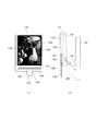
図1は本発明による表示装置および電子機器の実施例の構造に関する概要を示す図である。この図1では、表示装置を該表示装置に対応する基板上に実装した形態が表されており、図1(a)は正面図、図1(b)は側面図である。以下に図1を参照して説明する実施例は、例えば携帯情報端末(携帯電話機として機能するものである場合を含む)である電子機器であって、表示対象となるデータを表す表示信号を生成するために自己の本体内に設けられている回路部によって構成される表示信号生成部と、この表示信号生成部によって生成された表示信号に基づいて表示体に表示を行う表示部と、上述の表示信号生成部によって生成される表示信号をこの表示部に伝送する伝送経路に介挿された結合部とを含んで構成される。 FIG. 1 is a diagram showing an outline of the structure of an embodiment of a display device and an electronic apparatus according to the present invention. FIG. 1 shows a form in which a display device is mounted on a substrate corresponding to the display device. FIG. 1 (a) is a front view and FIG. 1 (b) is a side view. The embodiment described below with reference to FIG. 1 is an electronic device that is, for example, a portable information terminal (including a case that functions as a mobile phone), and generates a display signal representing data to be displayed. A display signal generation unit configured by a circuit unit provided in the main body of the display unit, a display unit that performs display on the display body based on the display signal generated by the display signal generation unit, And a coupling unit interposed in a transmission path for transmitting the display signal generated by the display signal generation unit to the display unit.
図示の例では、表示体として液晶表示体100を適用しているが、本発明はこれに限定されるものではなく、表示体に発光ダイオードやEL(エレクトロルミネッセンス)素子やプラズマディスプレイなどを使用したフラットパネル表示素子、また場合によってはCRT(陰極線管)などの表示素子を適用可能であり、これらを適用した場合にも同様の効果が得られる。
In the illustrated example, the liquid
液晶表示体100は図1に示すように2枚の透明板に封入された液晶表示パネル101と背面から照明するための導光板107で構成され本電子機器の表示部を構成するものであり、駆動用集積回路103が一体的に設けられている。102は電子機器本体側(これ以降、適宜「本体側」という)の回路基板であり、この表示体を適用して構成される電子機器による通話やメールの授受等々の本来の機能を賄うと共に、該表示体としての液晶表示体100に所要の表示を行うための表示信号を生成する表示信号生成部としての機能を営む。
As shown in FIG. 1, the
また、この回路基板102は、他の制御を行う回路が搭載されると共に当該液晶表示体100を自己(回路基板102)に図示しない支持部により固定し支持する。
回路基板102側から発せられる表示を行うための信号は、回路基板102側の無線送信部105と液晶表示体100側の無線受信部106とを含んで構成される結合部としての無線結合部104を通して伝送され、駆動用集積回路103に供給される。
In addition, the
A signal for performing display emitted from the
即ち、無線結合部104は表示信号生成部によって生成される表示信号を表示部に伝送する伝送経路に介挿され当該表示信号を無線で送出する無線送信部と前記表示部の表示体乃至該表示体を駆動する駆動回路が配された基板と一体的に構成され前記無線送信部から無線で送出された表示信号を受信する無線受信部とを含んで構成されている。無線結合部104の詳細については後述する。
That is, the
上述のように、当該液晶表示体100と回路基板102側とは無線結合部104を通して信号の伝送が行われるため、接触による接続をなくすことができ、従って、コネクタの信頼性に係る問題は根本的に解消する。尚、液晶表示体100やその駆動用集積回路103の電源の供給や駆動用集積回路に必要な制御信号やリセット信号などあまり高速性が要求されない信号や少数の信号線や電源線などは従来の方法によって接触によりコネクタで接続してもよい。
As described above, since the signal transmission is performed between the liquid
本例のように無線接続部で高速かつ多数のピンを要する信号の接続の機能を賄うことができれば残りの信号線は数も少なくこれらの信号線では接続に関する問題がないので、既述のような従来の課題は実質的に解決する。また同期信号のような一部の制御信号を有線接続で伝送するように構成すれば、無線接続の同期捕捉や追跡が非常に簡略化される効果もある。 As in this example, if the wireless connection unit can provide the function of connecting signals that require a high speed and a large number of pins, the remaining signal lines are few and there is no problem with connection with these signal lines. Such conventional problems are substantially solved. Further, if a part of the control signal such as a synchronization signal is transmitted by wired connection, there is an effect that the synchronization acquisition and tracking of the wireless connection is greatly simplified.
図2(a)及び図2(b)は図1を参照して簡単に説明した無線結合部の詳細を示す側面図である。図2において既述の図1と同じ構成要素については同一の参照番号を附して示し、それら各部自体の説明は省略する。
無線受信部を内蔵する集積回路205が基板201に実装され、この集積回路205は、液晶表示素子100のガラス上に実装された表示駆動用集積回路103にガラス上の配線を通して接続される。無線受信部を内蔵する集積回路205には信号受信のためのアンテナとして機能する導体部(受信アンテナ用導体)204が接続され、この導体部で受信した信号が集積回路205内のフロントエンドに入力される。
2 (a) and 2 (b) are side views showing details of the wireless coupling unit briefly described with reference to FIG. In FIG. 2, the same components as those in FIG. 1 described above are denoted by the same reference numerals, and the description of each part is omitted.
An
ここに、液晶表示素子100はガラス上に実装されるものに限られず、水晶基板やプラスチック上に形成される態様のものを適用可能である。これらの態様のものである場合には、上述の配線もこれら水晶基板やプラスチック上に設けられる。
尚、本発明の実施例において、受信用のアンテナを構成する受信用素子および送信用のアンテナを構成する送信用素子は、それらの素子が導体である態様、または、導体と誘電体とを組み合わせた態様、若しくは、導体と誘電体と磁性体とを組み合わせた態様の何れかの態様を、要求された仕様等に合わせて適用することができる。
Here, the liquid
In the embodiment of the present invention, the receiving element constituting the receiving antenna and the transmitting element constituting the transmitting antenna are such that the elements are conductors, or a combination of a conductor and a dielectric. Any of the above embodiments, or a combination of a conductor, a dielectric, and a magnetic body can be applied according to the required specifications.
表示のためのデータは本体側の回路基板102に搭載された回路で生成され、送信部を内蔵する集積回路202から送信アンテナとして機能する導体部(以下、送信アンテナ用導体という)203から当該データの伝搬を担う電磁波の信号として放射される。
本体側の回路基板102としては、例えば、両面基板、多層配線基板、ビルドアップ基板などを用いることができ、実装基板102の材質としては、例えば、ガラスエポキシ樹脂、BTレジン、アラミドとエポキシのコンポジットまたはセラミックなどを用いることができる。また、基板201としてはテープ基板またはフィルム基板などを用いるのが一般的であり材質としてはポリイミド樹脂などが多用される。
Data for display is generated by a circuit mounted on the
As the
また、集積回路205を基板201上に実装する方法としては、例えば、集積回路205を基板201上にフェースアップ実装する方法の他、集積回路205を基板201上にフリップチップ実装するようにしてもよい。例えば、集積回路205を基板201上にフリップチップ実装する場合、ACF(Anisotropic Conductive Film)、NCF(Nonconductive Film)接合、ACP(Anisotropic Conductive Paste)接合、NCP(Nonconductive Paste)接合などを用いることができる。
As a method for mounting the
図2(b)は図2(a)の基板201を折り曲げて液晶表示パネル101の裏側に受信用集積回路205と受信アンテナ用導体204を置く場合の構造を示す。これらは実装や電子機器のデザインによって適宜選択して適用する。
図3に送信用または受信用のアンテナとして機能する導体の例を示す。図3(a)は幅広い方形の導体301,302を置いて例えばその対向する角部で給電または受電する。図中303は受給電点を示す。尚、受給電点の位置は角部に設定することを必須とするものではなく、対向する辺の中央あるいはその他の適宜の部位に設定して支障はない。
FIG. 2B shows a structure when the
FIG. 3 shows an example of a conductor that functions as a transmitting or receiving antenna. In FIG. 3A, wide
図3(b)は図3(a)に示す導体部の実装方法を示す。図3(a)に示す導体を対向させて、表示体側の基板201に配せば受信アンテナ用導体204として機能し、また、本体側の基板102上に配せば送信アンテナ用導体203として機能する。図3(b)において、305および306はそれぞれ給電点および受電点である。
結合の度合いを高めるためにそれぞれのアンテナ用導体203、204の間に誘電体を挟んでも良い。あるいはそれぞれのアンテナ用導体203,204の上側(基板と反対側)に誘電体板(図3(b)310,309)を貼付し、その誘電体板を対向させる構造をとっても良い。
FIG. 3B shows a mounting method of the conductor portion shown in FIG. If the conductors shown in FIG. 3A are opposed to each other and placed on the
In order to increase the degree of coupling, a dielectric may be sandwiched between the
送信アンテナ用導体203および受信アンテナ用導体204の各対応する基板102、201を挟んで反対側に導体307、308を配する構成を採ることは推奨される。このような構成を採ることにより、これらの導体307、308によって無線結合部をその外側から略全面的に覆うと、この無線結合部から電磁波が漏洩せず、また外部からの強電界の影響も排除することができる。
It is recommended to adopt a configuration in which the
即ち、本実施例におけるように内部素子同士の結合に無線通信を適用してもその信号が漏洩し、例えば同じ筺体内の電子機器本来の機能である電話機能などへの混信や妨害が生じる懸念を払拭することができる。特に、携帯電話のように双方向の通信機能を有する電子機器では、同一筺体内に送信のための機能部が備えられているが、この送信のための機能部による強電界によって表示体と本体間の無線通信が妨害されることも防ぐことができる。 That is, even if wireless communication is applied to the coupling between internal elements as in this embodiment, the signal leaks, and there is a concern that interference or interference with the telephone function, which is the original function of an electronic device in the same housing, may occur. Can be wiped off. In particular, in an electronic device having a bidirectional communication function such as a mobile phone, a function unit for transmission is provided in the same housing, and the display body and the main body are caused by a strong electric field generated by the function unit for transmission. It is also possible to prevent the wireless communication between them from being interrupted.
上述のような構造をとる場合、給電点305または受電点306から既述の各導体側を見ると、導体301(送信アンテナ用導体203または受信アンテナ用導体204として機能する)と裏面の導体307または308とで構成されるコンデンサと導体302(送信アンテナ用導体203または受信アンテナ用導体204として機能する)と裏面の導体307または308とで構成されるコンデンサが直列接続されたコンデンサが現れる。
In the case of adopting the above-described structure, when the conductors described above are viewed from the
導体301または302の面積が大きいとこのコンデンサの容量も大きくなり受給電点でのマッチングを悪化させる。あるいは給電点305においては給電された電流がほとんどこのコンデンサ内を流れることになり受信側へのエネルギー伝達効率を悪化させ、また受電点306においては受信信号によって誘起された電流がこのコンデンサによって短絡されてしまい有効に取り出せなくなる。
この対策としては図3(c)に示す導体301a,302aのように内部を刳り貫くなどして導体面積を減少させ直列コンデンサの容量を減らしその効果を減じる方法がある。刳り貫かれた導体に沿って流れる電流によって電磁波を誘起して信号を効率よく受信側に伝送することが可能である。
When the area of the
As a countermeasure, there is a method of reducing the effect by reducing the conductor area by reducing the area of the conductor by piercing through the inside as in the
以上、図3(a)または図3(c)を参照して述べた方法はダイポール形のアンテナを変形したものに相当する。アンテナ機能を持たせるために導体を図3(d)に示すようなループ型にすることも可能である。この場合は、給電点305で給電された電流はループ型の導体203aを流れループアンテナの原理で信号エネルギーを放射する。また、受信側の導体204aはループ内に誘発される起電力を受電点306に誘起する。
ループ型導体203a、204aの間に磁気的な結合を強めるために磁性体を置いても良い。
The method described with reference to FIG. 3A or FIG. 3C corresponds to a modified dipole antenna. In order to provide an antenna function, the conductor may be a loop type as shown in FIG. In this case, the current fed at the
A magnetic material may be placed between the
図3(e)、(f)にそれぞれ図3(a),(b)の例、および、図3(d)の例におけるアンテナ用導体の伝送特性のシミュレーション結果を示す。
図3(e)は図3(a)に示すアンテナ用導体を図3(b)に示すように対向させた時の送受間の伝送特性(S21)である。
図3(f)は図3(d)に示すアンテナ用導体の配置にて送受間の伝送特性(S21)である。
図3(e)、および、図3(f)中で、dはアンテナ用導体間の距離を示す。シミュレーション時のそれぞれの寸法諸元は以下のとおり。
FIGS. 3E and 3F show the simulation results of the transmission characteristics of the antenna conductor in the examples of FIGS. 3A and 3B and the example of FIG. 3D, respectively.
FIG. 3E shows transmission characteristics (S 21 ) between transmission and reception when the antenna conductor shown in FIG. 3A is opposed to each other as shown in FIG. 3B.
FIG. 3F shows transmission characteristics (S 21 ) between transmission and reception with the antenna conductor arrangement shown in FIG.
In FIG. 3 (e) and FIG. 3 (f), d indicates the distance between the antenna conductors. The dimensions of each simulation are as follows.
図3(a),(b)
導体301,302
サイズ:1辺が5mmの正方形を0.2mm隔てて配置
材質: 厚さ12μの銅
基板 102,201
どちらも厚さ25μのポリイミド(比誘電率=5)、
裏面シールド307,308:なし
図3(d)
ループ導体203a、204a
サイズ:外形が3.5mmの正方形、線幅0.5mm
導体の材質、基板の材質等の他の諸元は図(a),(b)の例に同じ。
3 (a) and 3 (b)
Size: Squares with sides of 5 mm are spaced 0.2 mm apart
Material:
Both have a thickness of 25μ polyimide (relative permittivity = 5),
Back shield 307, 308: None FIG. 3 (d)
Size: External shape is 3.5mm square, line width is 0.5mm
Other specifications such as the material of the conductor and the material of the substrate are the same as in the examples of FIGS.
これらの図から判るように、送受間距離dを2mm程度以下にすると損失は10dB以下であり、伝送特性(S21)であらわされる伝送損失は極めて少ない。このようなアンテナ用導体の特性によって通信路を確保するためのリンクバジェットの組み立てが容易になり、また送信に必要な電磁波エネルギーを必要最小限の極めて低い値にすることが可能である。 As can be seen from these figures, when the distance d between transmission and reception is about 2 mm or less, the loss is 10 dB or less, and the transmission loss represented by the transmission characteristic (S 21 ) is extremely small. Such characteristics of the antenna conductor make it easy to assemble a link budget for securing a communication path, and make it possible to reduce the electromagnetic energy required for transmission to an extremely low value.
図3(a)のアンテナ用導体においてより小型を目指すために伝送特性を周波数の低い側にシフトすることが可能である。これは図3(g)に示すように図3(a)の導体に幅gで表す切れ目を入れてミアンダ型の素子を構成することによって達成される。ミアンダ型の素子を使ったアンテナはその共振周波数が低い側にシフトし小型のアンテナを実現できるが本発明のような場合にも同様の効果が得られる。 It is possible to shift the transmission characteristics to a lower frequency side in order to aim for a smaller size in the antenna conductor of FIG. As shown in FIG. 3 (g), this is achieved by forming a meander-type element by making a cut in the width g in the conductor of FIG. 3 (a). An antenna using a meander-type element can be shifted to a lower resonance frequency to realize a small antenna, but the same effect can be obtained in the case of the present invention.
図3(a)の導体にg=0.5mmの切れ目を入れたときのシミュレーション結果を図3(h)に示す。図3(h)から判るように伝送特性が改善された。特にd=1mm程度では損失が2dB以下でありこれは通常の物理接触によるコネクタの損失とも遜色ない値である。このようにして送受のアンテナ用導体のサイズを縮小することは更に送信に必要な電磁波エネルギーを少なく出来るので、外部に与える妨害を減らし、また物理サイズが小さいためシールドも容易になり外部からの妨害も軽減する効果がある。 FIG. 3 (h) shows the simulation result when a cut of g = 0.5 mm is made in the conductor of FIG. 3 (a). As can be seen from FIG. 3 (h), the transmission characteristics were improved. In particular, when d = 1 mm, the loss is 2 dB or less, which is comparable to the loss of the connector due to normal physical contact. By reducing the size of the antenna conductor for transmission and reception in this way, the electromagnetic wave energy required for transmission can be further reduced, so that the interference given to the outside is reduced, and the shield is easy because the physical size is small, so that the interference from the outside is reduced. Also has an effect of reducing.
図4に本発明による表示装置の実施例とそれを駆動する本体側の主要部を説明するブロック図を示す。本体側の回路基板102には、液晶表示体100に表示させるデータをCPU(図示せず)からCPUバス406を通して受け取り、後述する表示モジュール401に表示信号として順次出力する表示コントローラ405、および、表示コントローラ405からの信号を受けて無線伝送するべく変調をかけ送信アンテナ用導体409に送出する変調部404、ならびに、表示モジュール401が搭載されている。
FIG. 4 is a block diagram for explaining an embodiment of a display device according to the present invention and a main part on the main body side for driving the display device. The
この表示モジュール401には、送信アンテナ用導体409から無線信号を受けて後段に伝える受信アンテナ用導体408から信号を受け取り、該受け取った信号を復調する復調部403、この復調部403から信号を受け取り液晶表示体100を駆動する表示体駆動回路402が含まれる。
この実施例では、表示コントローラ405と表示体駆動回路402の同期を取るためのクロック信号や表示モジュール401側から表示コントローラ405に送信される信号(例えばビジー信号等)は、本体側の回路基板102の所定の線路410を通して有線で供給され、該供給された信号によって該当する各部はそれぞれ所定の機能を営む。
The
In this embodiment, a clock signal for synchronizing the
更に、表示モジュール401は、電源(Vdd,Vss)、バックライトの電源(Vbl)、リセット信号入力(RESET)などの信号端子407も持ち、それらも有線によって所定の場所に接続される。これらの線路によって伝送されるのは電源のエネルギーや低速の情報であり接続も容易であり、有線伝送によっても本願の課題としている問題を生じることはない。
Further, the
本発明による表示装置の無線結合部のように、極近距離で無線によって電気信号を伝送する場合は、その送受信点間の距離が使用される信号の波長の2π分の1以下(πは円周率)となる。半径が波長の2π分の1の球はラジアン球と呼ばれるが、本発明による表示装置の無線結合部はこのラジアン球内に収まっている。ラジアン球の中心に微小ループアンテナまたは微小ダイポールアンテナを置いたとき、それらのアンテナによって生じる電磁界の強さがラジアン球の中心からの距離に逆比例して減少する放射界、距離の2乗に反比例して減少する誘導界、距離の3乗に反比例して減少する静電界の3つが同じ値になる境界がちょうどラジアン球の表面となる。 When an electrical signal is transmitted wirelessly at a very short distance as in the wireless coupling part of the display device according to the present invention, the distance between the transmission and reception points is equal to or less than 1 / 2π of the wavelength of the signal used (π is a circle) Frequency). A sphere having a radius of 1 / 2π of a wavelength is called a radian sphere, and the wireless coupling portion of the display device according to the present invention is contained in the radian sphere. When a minute loop antenna or minute dipole antenna is placed at the center of a radiant sphere, the electromagnetic field generated by these antennas decreases in inverse proportion to the distance from the center of the radiant sphere. The boundary where the induction field that decreases inversely and the electrostatic field that decreases inversely proportional to the cube of the distance has the same value is the surface of the radiant sphere.
本発明による実施例では無線結合部で伝送される電磁波信号の波長は該電磁波信号が或る帯域に広がっているため、波長も1つの値ではなく或る範囲にわたって幅をもつ。
上述のような範囲において波長の値としてどの値を採用するかであるが、ここでは伝送される電磁波信号帯域内において最も長い波長を採用することにする。
また微小ループアンテナや微小ダイポールアンテナのように大きさを考慮しなくてよいのでラジアン球を考えればよいが、本実施例では送信アンテナ用導体、受信アンテナ用導体は有限の大きさを持つので、上述の3つの界が同じ大きさになる点の分布は球にはならない。信号の全帯域にわたってそのような性質を持つ面も存在しない。ここでは送受信のアンテナ用導体の最短距離が送受信のアンテナ用導体間の距離と考えることにする。
In the embodiment according to the present invention, the wavelength of the electromagnetic wave signal transmitted by the wireless coupling unit is spread over a certain range rather than a single value because the electromagnetic wave signal is spread over a certain band.
Which value is used as the wavelength value in the above-mentioned range, here, the longest wavelength in the transmitted electromagnetic wave signal band is adopted.
In addition, since it is not necessary to consider the size like a small loop antenna or a small dipole antenna, it is sufficient to consider a radiant sphere, but in this embodiment, the transmitting antenna conductor and the receiving antenna conductor have a finite size, The distribution of points where the above three fields have the same size does not become a sphere. There is no surface with such properties over the entire bandwidth of the signal. Here, the shortest distance between the transmitting and receiving antenna conductors is considered as the distance between the transmitting and receiving antenna conductors.
なぜならば、アンテナの大きさが無視できない様な至近距離では、信号帯域の低い側と高い側とでその伝送特性が大きく変わり帯域の伝送特性を悪化させる。また送受信のアンテナ用導体上の任意の2点間の距離は大きく変化しその距離が長いか短いかによってその2点間での伝送特性も大きく変動し、やはり帯域の伝送特性を悪化させる。
そのためなるべくアンテナ用導体の距離は離したいところである。逆にアンテナ用導体を近付けると外部に漏洩する電磁波エネルギーを小さくするためのシールド等の対策も容易になる上に伝送される信号エネルギーの損失も小さく出来る。
This is because, at close distances where the size of the antenna cannot be ignored, the transmission characteristics change greatly between the low side and the high side of the signal band, and the transmission characteristic of the band deteriorates. Also, the distance between any two points on the antenna conductor for transmission / reception changes greatly, and depending on whether the distance is long or short, the transmission characteristics between the two points also vary greatly, which also deteriorates the band transmission characteristics.
Therefore, it is desirable to keep the distance between the antenna conductors as much as possible. On the other hand, when the antenna conductor is brought closer, measures such as shielding for reducing electromagnetic wave energy leaking to the outside can be facilitated, and loss of transmitted signal energy can be reduced.
上記のような得失を勘案すると少なくとも送受信のアンテナ用導体の最小の距離が伝送される信号帯域内の最大波長の2π分の1以下とするのが妥当である。もちろん理想的には送受信のアンテナ用導体を可能な限り小さく構成し、送受信のアンテナ用導体全体を伝送する電磁波信号の帯域内の少なくとも中心周波数における波長の2π分の1を半径とする球の内部に収納することが望ましい。 Considering the advantages and disadvantages as described above, it is appropriate that at least the minimum distance between the transmitting and receiving antenna conductors is 1 / 2π or less of the maximum wavelength in the signal band to be transmitted. Of course, ideally, the antenna for transmitting and receiving antennas is made as small as possible, and the inside of a sphere having a radius of at least 1/2 of the wavelength at the center frequency in the band of the electromagnetic wave signal transmitted through the entire antenna conductor for transmitting and receiving It is desirable to store in.
従って、上述のように本発明による表示装置の無線結合部のような極近距離で行われる無線通信は放射界によって行われる従来の無線通信とは大きく性質が異なり、誘導界や静電界による影響やアンテナの大きさや信号の帯域も考慮しなければならない。
その影響を具体的に挙げれば、第一に送受信間でのエネルギーの損失率、いわゆるパスロスが従来のフリスの公式によって計算した値よりも大幅に小さくなる。これはラジアン球内であるため、誘導界や静電界によるエネルギー伝達の割合が大幅に増加するためである。
Therefore, as described above, the wireless communication performed at a very short distance, such as the wireless coupling part of the display device according to the present invention, is significantly different from the conventional wireless communication performed by the radiation field, and is affected by the induction field and the electrostatic field. Also consider the size of the antenna and the signal bandwidth.
Specifically, the energy loss rate between transmission and reception, the so-called path loss, is significantly smaller than the value calculated by the conventional Friis formula. This is because the rate of energy transfer by an induction field or an electrostatic field is greatly increased because it is in a radiant sphere.
第二に送受信間のアンテナは互いに相手の存在によってその特性が影響を受ける。従来の無線通信に用いられるアンテナは送受信間の距離が大きいため送信、または受信アンテナ単体で計算すればよく相手方のアンテナの存在がその特性に影響を与えることを考慮すする必要がなかった。しかし、本発明のような場合は送信、受信アンテナが互いにその特性に影響を及ぼす。放射界によってエネルギー放射を行う装置がアンテナであるとすれば、本願のような場合はそれに加えて静電界、誘導界のエネルギー伝達も考慮しなければならないので、もはやアンテナと呼べるかどうか疑問である。
上述において導体203や204、また、図3における301,302等を通常の如く単にアンテナ乃至アンテナ素子とのみ断言していないのはそのためである。本発明におけるように送受アンテナを極近付けた場合、その放射インピーダンスは遠方に相方がある場合に比較し減少し、帯域は広くなる傾向にある。
Secondly, the characteristics of antennas between transmission and reception are affected by each other's existence. Conventional antennas used for wireless communication have a large distance between transmission and reception, and it is only necessary to calculate for a transmission or reception antenna alone, and it is not necessary to consider that the presence of the other party's antenna affects its characteristics. However, in the case of the present invention, the transmitting and receiving antennas affect the characteristics of each other. If the device that radiates energy by the radiation field is an antenna, in the case of this application, in addition to that, it is necessary to consider the energy transfer of the electrostatic field and induction field, so it is questionable whether it can be called an antenna anymore. .
This is why the
第三に近接金属があっても従来のアンテナのようにその特性が大きく劣化することがない。従来のようにアンテナ単体で計算するときは近接金属等の影響を考慮しての計算は大掛かりになるのでそれらを省略し無視して計算し、影響を考慮するときはそれらを組み入れて改めて計算を行う。大抵の場合、それらを組み入れると特性が大幅に劣化する。本発明におけるような場合では送受アンテナが近接しているために単体で省略計算を行うことができず影響物を最初から組み入れて計算することになる。従ってたとえ劣化するとしても設計時にその劣化度合いも一緒に組み入れて計算するので、その影響は最初から排除されてしまう。 Third, even if there is a nearby metal, its characteristics are not greatly deteriorated unlike the conventional antenna. When calculating with a single antenna as in the past, the calculation taking into account the effects of nearby metals etc. becomes large, so omit them and calculate ignoring them. When considering the effects, incorporate them and calculate again. Do. In most cases, incorporating them will significantly degrade the properties. In the case of the present invention, since the transmitting and receiving antennas are close to each other, the omission calculation cannot be performed alone, and the influence object is incorporated from the beginning. Therefore, even if it deteriorates, the degree of deterioration is also calculated and calculated at the time of design, so the influence is eliminated from the beginning.
第四にマルチパスやフェーディングなどの伝播に関する特性劣化要因がない。これは送受信点がラジアン球内にあるからというよりも、そのような近距離であるため両者の間隔が固定され、それらが入り込む余地を物理的に排除してしまうためである。
図3(a)または図3(c)は静電界、図3(d)は誘導界による結合も大いに作用していると考えられる。特に図3(c)はループアンテナを対向させたというより相互誘導によっていわゆるM結合と考えることも可能である。
以上の考察は、無線結合部のリンクバジェットや回線設計を容易にし、また使用される送受信機回路の設計も容易にすることが可能である。
Fourth, there is no characteristic deterioration factor related to propagation such as multipath and fading. This is because the transmission / reception point is not in the radian sphere, but because it is such a short distance, the distance between the two is fixed and the room for them to enter is physically excluded.
3 (a) or 3 (c) is considered to be greatly affected by the electrostatic field, and FIG. 3 (d) is also strongly influenced by the induction field. In particular, FIG. 3C can be considered to be a so-called M coupling by mutual induction rather than facing the loop antennas.
The above considerations can facilitate the link budget and circuit design of the wireless coupling unit, and also facilitate the design of the transceiver circuit used.
図5は、上記考察に基づき設計された送受信部の一実施例の概要を説明するための図である。図5(a)にブロック図、図5(b)〜図5(e)に主要部分のタイム図を示す。
表示コントローラが発生する表示データは何本もの線路を通して並列に出力され端子516を通じて送信部集積回路525内部の並直変換回路(図中P/Sと表記)501に入力される。並直変換回路501では並列に受け取った表示データ信号を直列の信号に変換し1本のシリアルデータとしてパルス発生回路502に送出する。パルス発生回路502では送出するデータの値、即ち1,0に応じて所定のパルスを発生しバンドパスフィルタ(図中BPFと表記)504を通じて送信アンテナ用導体505に送出する。
FIG. 5 is a diagram for explaining an outline of an embodiment of a transmission / reception unit designed based on the above consideration. FIG. 5A shows a block diagram, and FIGS. 5B to 5E show time diagrams of main parts.
Display data generated by the display controller is output in parallel through a number of lines, and is input to a parallel-to-serial conversion circuit (denoted as P / S in the figure) 501 in the transmitter integrated
PLL(位相固定ループ)503は端子517に入力された表示コントローラやCPUが用いるクロック信号を受けて逓倍し並直変換回路501やパルス発生回路502で用いる高周波のクロックを再生する。この再生されたクロック信号は表示コントローラやCPUが用いるクロック信号と位相がそろっており同期しているため、送信アンテナ用導体505から送出されるパルスも同期させることができる。送信部に入力されるクロック信号はPLL503によって内部では必要な高周波のクロック信号が作り出されるので低い周波数の信号でよい。
A PLL (phase locked loop) 503 receives and multiplies the clock signal used by the display controller and CPU input to the terminal 517 and reproduces a high-frequency clock used by the parallel-to-
また表示データは並列信号として何本もの線路によって伝送されるのでこの部分でも周波数は低く接続は容易であり、またEMIなどの不要放射や外部からの妨害も少ない。唯一高周波が必要な並直変換後の表示データはパルス変調によって更に高周波広帯域の信号に変換されるが、従来のような有線による接続でないので、この部分の接続に関する従来の問題は一掃される。 Further, since display data is transmitted as a parallel signal through a number of lines, the frequency is low even in this portion and connection is easy, and unnecessary radiation such as EMI and interference from the outside are also small. The display data after the serial-to-parallel conversion that requires only a high frequency is converted into a signal having a higher frequency and a wide band by pulse modulation. However, since it is not a wired connection as in the prior art, the conventional problems related to this portion of connection are eliminated.
また、外部への干渉や、外部から受ける妨害も図3(b)を参照して述べた方法などによって完全に排除することが可能であり、このような構成をとることにより信頼性の高い低コストの接続を行うことができる。
送信アンテナ用導体505から発射された無線信号は受信アンテナ用導体507で受信されバンドパスフィルタ(図中BPFと表記)508を通して受信部集積回路526内部の低雑音増幅回路(図中LNAと表記)509に入力され増幅される。この信号はパルス検出回路513によって検出されたあと直並変換回路(図中S/Pと表記)514により並列信号に変換され表示データとして端子518より出力され液晶駆動回路に送出される。
Further, external interference and external interference can be completely eliminated by the method described with reference to FIG. 3 (b) and the like. Cost connection can be made.
A radio signal emitted from the transmitting
PLL512は送信側PLL503の基準信号となった表示コントローラやCPUが用いるクロック信号と同一の信号を受けて逓倍し、パルス検出回路513のパルス検出タイミングを設定する信号として、あるいは直並変換回路514で使用する信号として使用するクロック信号を再生する。この場合、送信側パルス発生回路502から受信側パルス検出回路513に到る経路の信号伝播遅延と同期がとれるように、セレクタ511によって回路に直列に介挿される遅延素子510の数を調整することによってクロック信号の遅延量を調節し、送受間の同期を取る。
The
この実施例では、受信部集積回路526の動作の制御を司る制御部(図中Controllerと表記)515やCPU(不図示)が用いるクロック信号は送信部集積回路525に端子517から入力されたクロック信号と同一のものが有線の線路(図中clockと表記)で供給され、また、受信部集積回路526の制御部515から送信部集積回路506動作の制御を司る制御部(図中Controllerと表記)への信号(例えばビジー信号等)も所定の線路(図中busyと表記)を通して有線で供給されるように構成されているため送受間の同期は完全に一致する。
受信側で同期捕捉や追跡の手続きが不要となり電子機器の構成を簡略化することが可能である。
In this embodiment, a clock signal used by a control unit (denoted as Controller in the figure) 515 that controls the operation of the reception unit integrated
It is possible to simplify the configuration of the electronic device because the receiving side does not require synchronization acquisition and tracking procedures.
図5(b)〜図5(e)は本実施例におけるタイム図を示す。図5(b)に示すクロック信号はPLL503や512の基準信号である。この信号の周波数は並直変換後の表示データのビットレートよりずっと低周波であるため同図では信号の立ち上がりのみ図示している。PLL503はこの信号を逓倍し並直変換回路501やパルス発生回路502またはパルス検出に必要なクロック信号を作り出す(図5(c))。
FIG. 5B to FIG. 5E show time charts in this embodiment. The clock signal shown in FIG. 5B is a reference signal for the
パルス発生回路502によって発生するパルス信号は図5(e)に実線で示すパルス520のように送信する表示信号(図5(d))の値が1のときパルスを発生し、0のときは何も発生しないOOK(On Off Keying)変調や同図に破線521で示すように1のときと0のときでパルスの極性を変更するBPM(Bi−Phase Modulation)などを適用可能である。
この他に、パルスの位置を変更するPPM(Pulse Position Modulation)などを適用してもよい。
The pulse signal generated by the
In addition, PPM (Pulse Position Modulation) that changes the position of the pulse may be applied.
本実施例のようにパルスを用いた通信はインパルスラジオ通信(IR通信)と呼ばれ、ウルトラワイドバンド通信(UWB通信)の一形態である。UWB通信ではその信号スペクトルが広くなるが通信距離を短く取るにつれて可能な伝送速度が急激に上昇する。即ち近距離ほど高い伝送速度が可能となる。この性質を利用すると、従来は並列データとして低速の多数のデータ伝送路を用いて伝送していた大量のデータを単一の無線伝送路を用いて高速な直列データとして伝送することが可能である。 Communication using pulses as in this embodiment is called impulse radio communication (IR communication) and is a form of ultra-wideband communication (UWB communication). In UWB communication, the signal spectrum is widened, but the possible transmission rate increases rapidly as the communication distance is shortened. That is, a higher transmission speed is possible at a shorter distance. By utilizing this property, it is possible to transmit a large amount of data as high-speed serial data using a single wireless transmission line, which was conventionally transmitted using a large number of low-speed data transmission lines as parallel data. .
またUWB通信はその信号の帯域が極めて広いため単位帯域あたりのエネルギー密度はきわめて低くなる。そのため他の通信システムで使用する信号帯域と帯域が重なってもその影響はきわめて小さい。反対に他の通信システムからの信号が受信機に混入しても受信機の復調時に妨害波は拡散されその影響を排除できる。
またUWB通信は従来の変調操作のように周波数軸での操作を含まないため完全に時間軸上だけの処理で実現が可能であり回路の簡略化も可能である。
In addition, since UWB communication has a very wide signal band, the energy density per unit band is extremely low. Therefore, even if the signal band used in other communication systems overlaps, the influence is extremely small. On the contrary, even if a signal from another communication system is mixed in the receiver, the interference wave is spread at the time of demodulation of the receiver and the influence can be eliminated.
In addition, UWB communication does not include an operation on the frequency axis unlike a conventional modulation operation, and thus can be realized by processing only on the time axis, and the circuit can be simplified.
本実施例では上記に述べたように送受信のアンテナ用導体がもともと近い位置に有るので送信する電磁波エネルギーを必要最小限に抑えることが可能であり、更に送受信のアンテナ用導体をシールドするなどの対策によって外部へ漏洩する電磁波エネルギーを最小とし、あるいは、外部から妨害波として混入するエネルギーを最小化することも可能である。
これらの対策と上記に述べたUWB通信が持つ本質的な性質によって、従来の物理接触によるコネクタを無線化することが可能となる。従来の課題であったコネクタの信頼性やコスト、他に与える干渉などの妨害やまたは他からの妨害耐性の特性において大きく改善することが可能となる。
In this embodiment, since the transmitting / receiving antenna conductor is originally close as described above, it is possible to suppress the electromagnetic wave energy to be transmitted to the minimum necessary, and further measures such as shielding the transmitting / receiving antenna conductor. It is also possible to minimize the electromagnetic wave energy leaking to the outside or to minimize the energy mixed as an interference wave from the outside.
These measures and the essential properties of the UWB communication described above make it possible to wirelessly use a conventional connector based on physical contact. It is possible to greatly improve the reliability and cost of the connector, which has been a problem in the past, and the characteristics of interference such as interference given to others and resistance to interference from others.
本実施例では、パルス通信を用いるとその特性が生かせることを示したが、送受信の変調方式として従来の周波数変調や振幅変調、位相変調を用いてもよい。これらの変調を用いた場合には本実施例のように1本のシリアル信号として伝送しようとするとその周波数帯域を非常に広くしなければならないがパルス通信に要する帯域ほどは広い帯域は要求されないので場合によって使い分けることが可能である。
またこれらの変調方式を用いた場合は、符号分割多重などの技術によって並列データのまま多重化伝送することも可能である。こうすると伝送路あたりの転送速度を余り高くしないで大量のデータを伝送することが可能である。
In the present embodiment, it has been shown that the characteristics can be utilized when pulse communication is used, but conventional frequency modulation, amplitude modulation, and phase modulation may be used as a transmission / reception modulation scheme. When these modulations are used, if the transmission is made as one serial signal as in the present embodiment, the frequency band must be very wide, but a band as wide as that required for pulse communication is not required. It can be used properly depending on the situation.
When these modulation methods are used, it is also possible to multiplex and transmit parallel data as it is by a technique such as code division multiplexing. This makes it possible to transmit a large amount of data without increasing the transfer rate per transmission path.
上述の実施例1ではアンテナを構成する素子(送信用素子、受信用素子)を基板上の導電性のパターンによって形成したが、次に、実施例2として、送信用素子、受信用素子を各対応する送信部あるいは受信部のどちらか一方あるいは両方の半導体集積基板上に形成した例について説明する。
まず、半導体集積基板上にアンテナ用導体を形成した場合の実装形態について説明し、具体的にアンテナ用導体を半導体基板上に形成する方法は後述する。
In the first embodiment, the elements (transmitting elements and receiving elements) constituting the antenna are formed by conductive patterns on the substrate. Next, as the second embodiment, the transmitting elements and the receiving elements are provided. An example in which one or both of the corresponding transmitter and receiver are formed on the semiconductor integrated substrate will be described.
First, a mounting form in the case where an antenna conductor is formed on a semiconductor integrated substrate will be described, and a method for specifically forming the antenna conductor on the semiconductor substrate will be described later.
図6(a)は受信部集積回路601上にアンテナ用導体を形成した場合の実装形態を示す。このようにアンテナ用導体を集積回路に含むことが可能であれば、図6(b)のように表示駆動回路を内蔵する集積回路602に受信部回路およびアンテナ用導体も一緒に搭載することが可能である。このようにすれば集積回路のチップ数を減らし、また表示体駆動回路と受信部回路との間の配線もなくすことができるので装置の部品点数および配線数が減り信頼性向上、コストダウンに効果がある。
FIG. 6A shows a mounting form when an antenna conductor is formed on the receiver integrated
この場合基板603は不要になるが、他の配線、即ち図4におけるリセットや電源の配線407またはクロックや制御信号410のために使用することができる。
図6(c)は送信部のアンテナ用導体も送信部半導体集積回路604に含む場合である。また、図6(d)では表示駆動回路と受信部回路を同一の集積回路605に集積し受信のアンテナ用導体は基板201上のパターン204で形成する。
In this case, the
FIG. 6C shows a case where the antenna conductor of the transmitter is also included in the transmitter semiconductor integrated
一般にアンテナ素子を半導体集積回路上に形成した場合はその放射効率が極端に悪化し数GHzの周波数帯では約0.01%程度である。
送信側ではこの損失を送信電力の増加によって補償することができるが受信側での損失を補償するために送信電力を上げることは一般的にはできない。なぜならば受信側での損失補償のために送信側の電力を増加させるということは無線伝送路での信号強度(放射電界強度)を上げることであり、そうすると他に与える妨害エネルギーも増大してしまうためである。放射電界強度は法規制によって上限が定められており、むやみに信号強度を増やすことはできない。従って、図6(d)の構造が最も理に適った方法となる。
In general, when an antenna element is formed on a semiconductor integrated circuit, its radiation efficiency is extremely deteriorated and is about 0.01% in a frequency band of several GHz.
Although this loss can be compensated for by increasing the transmission power on the transmission side, it is generally impossible to increase the transmission power to compensate for the loss on the reception side. This is because increasing the power on the transmitting side to compensate for loss on the receiving side means increasing the signal strength (radiated electric field strength) on the wireless transmission path, and this will also increase other interference energy. Because. The upper limit of the radiated electric field intensity is set by legal regulations, and the signal intensity cannot be increased unnecessarily. Therefore, the structure of FIG. 6D is the most reasonable method.
この場合、無線信号による伝送距離が極端に近いため不要放射が問題になるような強い信号を必要としないし、また不要放射を防ぐためのシールドなどの方法も図3(b)を参照して既述のように簡単である。また、上記放射効率0.01%というのは放射界の場合であって、本実施例のような無線接続がラジアン球内部で行われる場合は、それに加えて誘導界や静電界による信号エネルギー伝送も用いることができるため、効率はこれよりはよい値を示す。これらの理由によって図6(a)〜図6(c)の方法も十分実用性がある。 In this case, since the transmission distance by the radio signal is extremely short, a strong signal that causes unnecessary radiation is not required, and a method such as shielding for preventing unnecessary radiation is also referred to FIG. It's as simple as already mentioned. The radiation efficiency of 0.01% is in the case of a radiation field. When wireless connection is performed inside a radiant sphere as in this embodiment, in addition to this, signal energy transmission by an induction field or an electrostatic field is performed. Efficiency can be better than this. For these reasons, the methods of FIGS. 6A to 6C are sufficiently practical.
図7にアンテナ用導体を半導体集積回路上に形成する場合を例示する。図7(a)は全体概要を示す図。図7(b)は断面図、図7(c)は給電点部分を拡大した図である。
アンテナ用導体701は集積回路基板705上に導電層を用いて形成する。通常の半導体集積回路プロセスではアルミニウムや銅などのメタル層が用いられる。図7(a)に示すような線状のアンテナ素子を形成するのが集積回路基板上で広い面積を必要とせず都合がよい。本実施例では集積回路基板705の周辺部に張った折り曲げダイポール形のアンテナを示す。702はその給電点であり図7(c)にその拡大図を示す。
FIG. 7 illustrates the case where the antenna conductor is formed on the semiconductor integrated circuit. FIG. 7A is a diagram showing an overview. FIG. 7B is a cross-sectional view, and FIG. 7C is an enlarged view of a feeding point portion.
The
図7(b)は実装時の断面図の例であり、基板703は図2における本体側基板102、または表示体側基板201に相当する。704は基板703上に設けた導電層であり集積回路基板705の電位を固定するとともにアンテナ用導体701のシールドも兼ねて不要放射や外部からの妨害を遮断する。アンテナ用導体701と集積回路基板705とは二酸化珪素のような絶縁層706によって絶縁される。
この絶縁層が薄いと通常は放射効率が極端に悪化し、また周波数帯域も狭くなるが集積回路基板705による損失が大きいため周波数帯域は狭くならないで寧ろ広がる。損失がかなり大きくても通信距離が極端に近いため実用上の問題はなく、寧ろその損失が必要な周波数帯域を保証してくれる。
FIG. 7B is an example of a cross-sectional view at the time of mounting, and the
If the insulating layer is thin, the radiation efficiency is usually extremely deteriorated and the frequency band is narrowed. However, the loss due to the integrated
集積回路基板705として高抵抗基板を用いる、またはSOI(Silicon On Insulator)構造などで絶縁基板上に極薄い半導体層を形成し集積回路を搭載するとともにアンテナ用導体701直下から導電層を排除することもできる。この場合はアンテナとしての放射効率を改善するが帯域は狭くなる方向である。なおSOIの場合は半導体基板電位をチップの裏側で取る必要がないので導体層704を基板703の反対側におき集積回路基板705から離すことが可能になり更に高い効率のアンテナ素子を集積回路上に搭載することが可能である。
A high resistance substrate is used as the
図7(c)は上述の集積回路基板705上の導体素子701を駆動する回路例を示しており、送信アンテナとして機能するように構成されている場合の例である。
図7(c)において、集積回路基板705には相補型のMOSトランジスタM1、M2が形成されている。ここで、MOSトランジスタM1において、集積回路基板705上に形成されたゲート716が設けられるとともに、ゲート716を挟み込むようにして配置されたドレイン712およびソースが集積回路基板705に形成されている。
FIG. 7C shows an example of a circuit for driving the
In FIG. 7C, complementary MOS transistors M1 and M2 are formed on the
また、MOSトランジスタM2において、集積回路基板705上に形成されたゲート714が設けられるとともに、ゲート714を挟み込むようにして配置されたドレイン707およびソースが集積回路基板705に形成されている。
なお、一点鎖線711はP型またはN型のMOSトランジスタM1、M2を形成するためのウェル境界を表す。ここで、MOSトランジスタM1、M2のドレイン707、712は、ドレインコンタクト713、715をそれぞれ介して導体層に接続されている。そして、ドレイン707、712に接続された導体層と同一の導体層によってアンテナの導体素子701が形成され、MOSトランジスタM1、M2のドレイン707、712が、アンテナ用導体素子701を形成する導体層に接続されている。
In the MOS transistor M2, a
An alternate long and
また、MOSトランジスタM1、M2のゲート716、714は、ゲートコンタクトをそれぞれ介して導体層710に接続されている。なお、MOSトランジスタM1、M2のゲート716、714は通常ポリシリコンにより作られ、導体層710,701はアルミニウム(Al)などによって作られる。そして、この2つのゲート714、716は導体層710により接続され送信信号の入力となる。
The
また、MOSトランジスタM1、M2のソースは、ソースコンタクトをそれぞれ介して導体層708、709にそれぞれ接続されている。そして、MOSトランジスタM1、M2のソースは、導体層708、709をそれぞれ介して電源に接続される。
これにより、ボンディンングパッドやボンディンングワイヤを介在させることなく、MOSトランジスタM1、M2のドレイン712、707とアンテナの導体素子701とを接続することが可能となり、寄生インダクタンスや浮遊容量の影響を低減させることができる。
なお、送信アンテナ(用)導体の場合には導体素子701はドレイン712、707に接続するが、受信アンテナ(用)導体の場合には導体素子701は信号の受け口即ちゲート710(ソース接地増幅回路を用いる場合)またはソース709、708(ゲート接地増幅回路を用いる場合)に接続されることになる。
The sources of the MOS transistors M1 and M2 are connected to the conductor layers 708 and 709 via source contacts, respectively. The sources of the MOS transistors M1 and M2 are connected to the power supply via the conductor layers 708 and 709, respectively.
As a result, it becomes possible to connect the
In the case of the transmitting antenna (use) conductor, the
なお、図7(c)における717は集積回路基板705の外縁を示す線である。アンテナ用導体701は線状の導体として集積回路基板の周辺に沿って置くと他の回路の集積などの邪魔にならず能率がよい。アンテナ用導体701と集積回路基板705の外縁717の間に、またはアンテナ用導体の内側に、集積回路と外部との信号やり取りのためのボンディングパッドなどを置いても良い。
以上述べた本実施例のようにアンテナ用導体を含む送受信部を半導体集積回路上に搭載すれば部品点数や信号線の接続本数を大幅に削減し、信頼性の向上、実装面積の節減、小型化、部品コストの削減に大きな効果がある。
Note that
If the transmitter / receiver including the antenna conductor is mounted on the semiconductor integrated circuit as in the above-described embodiment, the number of components and the number of signal lines are greatly reduced, and the reliability is improved, the mounting area is reduced, and the size is reduced. This has a great effect on reducing the cost of parts.
図8に他の実施例のブロック図を示す。本実施例では電源の供給や表示側からの信号も無線接続して完全にコネクタレス化を図る例である。
図8において既述の図5との対応部には同一の参照符号を附して示し、それら各部の各個の説明は省略する。
表示体側で使用する電源は本体側からコイル812,813を通じて相互誘導で伝送される。本体側である送信部集積回路525aでは端子517に入力されるクロック信号を駆動回路801で電力増幅し送信コイル812を駆動する。受信部集積回路526a側のコイル813は相互誘導によりコイル812からエネルギーを受け取り整流回路802で整流し電源エネルギーを取り出し、回路や表示体に供給する。同時にコイル813で受けた信号からクロック信号を取り出し、PLL512の基準信号や受信部回路の同期信号として利用する。
FIG. 8 shows a block diagram of another embodiment. In this embodiment, power supply and signals from the display side are wirelessly connected to achieve a complete connector-less operation.
In FIG. 8, the same reference numerals are given to the corresponding parts to FIG. 5 described above, and description of each part will be omitted.
A power source used on the display body side is transmitted from the main body side through
即ち、コイル812およびコイル813は、電子機器の本体内に設けられ表示信号を生成する表示信号生成部が配置された基板側に設けられている電源供給機能を有する回路としての駆動回路801から表示体のある表示部側に相互誘導によって非接触で電力を供給する配電用結合部を構成している。
また、表示体側(526a)から本体側(525a)に送出される信号は表示データが本体側から送られる方法と同様の方法で、表示体側から本体側に送出する。即ち表示体側コントローラ515が発するビジー信号などの信号はパルス発生回路803によりパルス変調されバンドパスフィルタ808を通じ送信アンテナ用導体811から本体側に送出される。本体側では受信アンテナ用導体810にて信号を受け取りバンドパスフィルタ809を通じ受信回路804で復調し本体側コントローラ506に出力する。
That is, the
The signal sent from the display body side (526a) to the main body side (525a) is sent from the display body side to the main body side in the same manner as the display data is sent from the main body side. That is, a signal such as a busy signal generated by the display-body-
バンドパスフィルタは与干渉性、耐干渉性の条件が満足できれば省略が可能である。また送信アンテナ用導体811とコイル813、受信アンテナ用導体810とコイル812は適当な合成回路によって信号合成することにより共用が可能である。共用しても使用する周波数帯域が大幅に違うのでバンドパスフィルタ808,809の働きによって両者の信号は確実に分離することができる。
The band-pass filter can be omitted if conditions for coherence and interference resistance can be satisfied. The
上記のような構成により、信号伝送および電源のエネルギー伝送を無線化することが可能となる。表示体の高解像度化による高い伝送レートにも多数の信号線を必要とせず、また、電源の接触による接続も不要となるので、コネクタなどの実装部品を省略でき、実装上の効果とコスト的な効果が大きい上に、EMI等の従来の諸々の課題も一気に解決できる。 With the above configuration, it is possible to wirelessly perform signal transmission and power transmission of power. The high transmission rate due to the high resolution of the display does not require a large number of signal lines, and there is no need for connection by contact with the power supply. In addition to the great effects, various conventional problems such as EMI can be solved at once.
図9に本発明による電子機器または表示装置に用いる送受信の他の実施例を示すブロック図を、また図10にその動作を示すタイム図を示す。本実施例では特にUWB通信の妨害排除能力を生かした構成例を示している。
パルス発生回路901は、端子903に印加された起動信号a(図10(a))を受けてパルスを発生する。その際、端子904に入力される送信データb(図10(b))の値に従って切り替え変調される。この変調の方式としてパルスの2相変調(BPM:Bi−Phase Modulation)やパルス位置変調(PPM:Pulse Position Modulation)を適用することができる。
FIG. 9 is a block diagram showing another embodiment of transmission / reception used in the electronic apparatus or display device according to the present invention, and FIG. 10 is a time chart showing the operation thereof. In the present embodiment, a configuration example in which the interference eliminating capability of UWB communication is utilized is shown.
The
パルス発生回路に平衡型のパルス発生回路を用いると上記の実施例で述べた平衡型のアンテナ902を駆動することができる。図10(c)、(d)は平衡型アンテナ902のそれぞれ端子に与えられる信号波形である。その差は図10(d)−(c)に示すような信号波形となる。図10(d)−(c)ではBPMの場合を示している。即ち信号bが0のときは差動信号d−c(同図(d)−(c))が負側から始まる極性のパルスを発生し、bが1の時は正側から始まる極性のパルスを発生する。
When a balanced pulse generating circuit is used as the pulse generating circuit, the
図10(j)にBPM信号波形のアイパターンを示す。送信データの値によってその極性を反転させる。また変調方式としては図10(k)に示すようなPPMを用いることも可能である。この方式は送出するデータの値によってそのパルス位置を変更する。図ではパルスの1/2周期ずらした場合を例示している。
パルス発生回路を2つ設けそれぞれペアとして互いに直交するパルスを発生させこれらをI,Q信号として、I,Qのそれぞれの信号に変調する4相変調(QPM:Quadrature Phase Modulation)も可能である。
FIG. 10J shows an eye pattern of the BPM signal waveform. The polarity is inverted depending on the value of the transmission data. As a modulation method, a PPM as shown in FIG. 10 (k) can be used. In this method, the pulse position is changed according to the value of data to be transmitted. In the figure, a case where the pulse is shifted by 1/2 period is illustrated.
Four pulse generation circuits (QPM: Quadrature Phase Modulation) are also possible, in which two pulse generation circuits are provided to generate pulses orthogonal to each other as a pair and modulate them into I and Q signals, respectively.
アンテナ905以降は受信回路の構成を示す。即ち受信アンテナ905で受信されたUWBパルス信号は低雑音増幅回路906で増幅し(図10(e)に差動出力の差分のみ示す,以下同じ)、I,Qのミキサ回路907,908に入力される。ミキサ回路907,908はテンプレートパルス発生回路909によって発生された互いに直交するテンプレートパルスf、g(図10(f)、(g))との乗算を行い積分回路910,911に送る。
The
ミキサ回路907,908の出力は図10(h)、(i)に示す。図10(e)〜(i)ではその動作が良くわかるように故意にテンプレートパルスと受信信号の同期が外れている時を示している。通常動作時においてはミキサ出力h、iが最大のSN比となるように同期を取る。
積分回路910,911ではミキサ回路907,908で混合(乗算)した信号の高域成分を取り除き復調を行う。判別回路912はそれぞれの信号の強度を見て送信されたビットを判断し元の送信データ913に戻す。
The outputs of the
The
ここでテンプレートパルス発生回路909として直交するテンプレートI,Qのそれぞれについて差動出力の回路が使用できる。差動出力のパルス発生回路は低雑音増幅回路906やミキサ回路907,908を差動式の回路を使用することを可能とする。差動式の回路は同相ノイズをキャンセルでき、また低電圧動作に適しており低電力低雑音の機器構成に都合が良い。またIQのテンプレートを用いると、QPMのときのみでなくBPMやPPMでも効率の良い受信が可能となる。即ちBPMやPPMの変調時において、Iチャネルをデータの復調にあてて、Qチャネルをトラッキングに使うなどの方法を採ることが可能である。なぜならQチャネル出力を常に0になるようにテンプレート発生のタイミングを調整すればIチャネルではその出力振幅値が最大となるのでこのような制御によって同期検波のトラッキングが可能となる。
Here, as the template
以上のような送受信機を構成すると外部の他の無線通信システムへ与える妨害や、他の無線通信システムで送信された非常に強い電磁波から受ける妨害を最小限に抑制することが可能である。
即ち、送信側ではパルス発生回路901の働きによって送信データが非常に広いスペクトル帯域の電磁波信号に変換されるが、帯域が広いためにそのエネルギー密度はきわめて低くなる。従って外部の他の通信システムで使用する無線通信の帯域内でのエネルギーは低く、しかもそれらのシステムで用いる信号との相関は低いため妨害波最小となる。また外部から妨害波となって受信される外部通信システムの信号はミキサ回路907,908によってテンプレートパルス発生回路909が発生するテンプレートパルスの帯域程度に拡散される。逆にアンテナ902によって送信された信号はテンプレートとの相関が強いために逆拡散され大きな信号となってミキサ回路907,908から出力される。これによって外部の強い信号の妨害波最小限に抑制することが可能である。
When the transceiver as described above is configured, it is possible to minimize disturbances to other external wireless communication systems and interference from very strong electromagnetic waves transmitted by other wireless communication systems.
That is, on the transmission side, the transmission data is converted into an electromagnetic wave signal having a very wide spectrum band by the action of the
上記の他の実施例で述べたようにアンテナ用導体の距離は小さく、送信機からの電磁波エネルギーはもともと小さい上に、距離に反比例して減衰する放射界のみでなく、距離の2乗,3乗に反比例して減衰する誘導界や誘電界も利用できるので外部へ漏れる電磁波エネルギーは小さい。その上、送受信アンテナ用導体には簡単にシールドを施すことが可能であり更に外部漏洩、外部からの混入を少なくする。更に加えてUWB通信の妨害排除能力を利用するため外乱に対して極めてロバスト(強靭)となる。 As described in the other embodiments above, the distance of the antenna conductor is small, the electromagnetic wave energy from the transmitter is originally small, and not only the radiation field attenuated in inverse proportion to the distance but also the square of the distance, 3 Since an induction field or a dielectric field that attenuates in inverse proportion to the power can be used, electromagnetic energy leaking to the outside is small. In addition, it is possible to easily shield the transmission / reception antenna conductor, and further reduce external leakage and external contamination. In addition, since it uses the interference rejection capability of UWB communication, it is extremely robust against disturbance.
以上のような構成によれば、たとえば携帯電話端末のような小さい筐体内に強い電波を発信する送信機が同居するようなシステムにおいても電話機能の送信機信号の妨害を受けることはない。また遠方の微弱電波を受信する受信機への妨害や外部機器への妨害となる不要放射も従来の物理接触によるコネクタよりも小さくすることが可能である。
また本回路をCMOS集積回路で実現すれば、パルス発生時の遷移時間でしか電力を消費せず、いわゆるアイドリングカレントがない。通信機に応用した場合は伝送する情報量(ビットレート)に応じて常に最小の消費電力で作動させることが可能である。
According to the above configuration, even in a system in which a transmitter that transmits strong radio waves coexists in a small casing such as a mobile phone terminal, the transmitter signal of the telephone function is not disturbed. In addition, unnecessary radiation that interferes with a receiver that receives a weak radio wave in the distance and that interferes with an external device can be made smaller than that of a conventional physical contact connector.
If this circuit is realized by a CMOS integrated circuit, power is consumed only during the transition time at the time of pulse generation, and there is no so-called idling current. When applied to a communication device, it is possible to always operate with minimum power consumption according to the amount of information (bit rate) to be transmitted.
実施例1ではアンテナ用導体は基板上の導電性のパターンによって形成し、また実施例2では送受信のアンテナ用導体のどちらか一方あるいは両方を半導体集積基板上に形成したが、次に、実施例5として、アンテナ用導体を、液晶表示体を構成するガラス基板上に形成した例について説明する。
アクティブマトリクス型液晶表示体はスイッチング素子などの能動素子を表示体パネルを形成するガラス等の基板上に作り込んだ表示体である。アクティブ素子としてガラス基板上に形成された結晶シリコンやアモルファスシリコン膜上に薄膜トランジスタを形成したものが多用されている。
In the first embodiment, the antenna conductor is formed by a conductive pattern on the substrate. In the second embodiment, either one or both of the antenna conductors for transmission and reception are formed on the semiconductor integrated substrate. 5, an example in which an antenna conductor is formed on a glass substrate constituting a liquid crystal display body will be described.
An active matrix type liquid crystal display is a display in which active elements such as switching elements are formed on a substrate such as glass forming a display panel. As an active element, a thin film transistor formed on a crystalline silicon or amorphous silicon film formed on a glass substrate is often used.
ここに、基板はガラス基板に限られず、水晶基板やプラスチック基板等も適用され得る。また、表示体としてEL(有機EL)やSED等も適用され得る。
これらの素子は通常の単結晶半導体基板上に形成されたトランジスタなどの素子に比較しスイッチング速度その他の性能は良くないが液晶パネルに一体化して形成できるために画素のスイッチングのほかにマトリックスのドライバなどにも使用される。
この素子を用いて本発明を構成する要素となる無線受信部または送信部およびアンテナ用導体を含む回路または素子の一部または全部を形成することが可能である。
Here, the substrate is not limited to a glass substrate, and a quartz substrate, a plastic substrate, or the like can also be applied. Moreover, EL (organic EL), SED, etc. can be applied as a display body.
These devices are not as good in switching speed and other performance as devices such as transistors formed on a normal single crystal semiconductor substrate, but they can be formed integrally with a liquid crystal panel. Also used for.
By using this element, it is possible to form part or all of a circuit or an element including a radio reception unit or transmission unit and an antenna conductor, which are elements constituting the present invention.
図11を参照して更に詳しく説明する。図11(a)は表示体の全体を説明する正面図、図11(b)は無線結合部を詳しく説明する側面図である。図11において、既述の図1、または図2との対応部には同一の参照符号を付して示し、それら各個の部分についての説明は省略する。
液晶表示体は2枚のガラスなどの基板1101,1102に液晶層を挟んで構成される。これらの基板1101,1102上には液晶画素の配線やスイッチング素子が形成される。図11では液晶のXドライバ1103、およびYドライバ1108が下側の基板1102に形成されている例を示す。
This will be described in more detail with reference to FIG. FIG. 11A is a front view illustrating the entire display body, and FIG. 11B is a side view illustrating the wireless coupling unit in detail. In FIG. 11, the same reference numerals are given to the corresponding parts to those in FIG. 1 or 2 described above, and description of these individual parts is omitted.
The liquid crystal display is configured by sandwiching a liquid crystal layer between two
表示エリア1109には薄膜トランジスタなどで画素毎にスイッチング素子が形成され、これらのスイッチング素子を駆動するドライバは基板に同様のプロセスで形成される。
本実施例では下側基板1102にXドライバ1103、Yドライバ1108を形成した例を示す。送信アンテナ用導体203から放射された表示データの信号は表示体の基板1102上に形成された受信アンテナ用導体1104によって受信される。
In the
In this embodiment, an example in which an
本実施例では受信アンテナ用導体1104は液晶表示体上の配線を形成する導電層によって作られている。液晶表示体ではインジウム錫酸化膜(ITO)等による透明の導電膜を用いるのが一般的である。この膜は抵抗率が高いため金属層などを蒸着などによって付加的に形成しその導電率を高めることもできる。
一般に表示体基板上に形成される導電層は抵抗率が高くこれをアンテナとして使用するには能率が悪いが抵抗が高いので帯域は広く取れる。効率が悪い点は送信側の電力を増やすことによってカバーできる。
In this embodiment, the receiving
In general, a conductive layer formed on a display substrate has a high resistivity and is not efficient for using it as an antenna. However, since the resistance is high, a wide band can be obtained. The inefficiency can be covered by increasing the power on the transmission side.
送信側の電力を増やすことは外部へ与える影響を増大させるが、本実施例のような場合は送受間の距離が非常に近いため外部へ影響するほどの電力増大は必要ない。また、実施例2のように半導体集積回路基板上にアンテナ用導体を形成する場合に比較しそのサイズを大きくすることが可能であり、使用する周波数帯の選択幅が広がり外部への影響の少ない周波数帯を選択することも可能である。また上記に述べたようなシールドなどの対策を施すこともできる。 Increasing the power on the transmission side increases the influence on the outside, but in the case of this embodiment, since the distance between transmission and reception is very close, the increase in power that affects the outside is not necessary. Further, the size of the antenna conductor can be increased as compared with the case where the antenna conductor is formed on the semiconductor integrated circuit substrate as in the second embodiment, and the selection range of the frequency band to be used is widened and the influence on the outside is small. It is also possible to select a frequency band. It is also possible to take measures such as shielding as described above.
基板1106は電源を表示体に供給するために、あるいは図4または図5において説明した低速の信号(図4の410,407)等を接続するために表示体の基板1102上に設けられる。テープ基板またはフィルム基板などを用いるのが一般的であり材質としてはポリイミド樹脂などが多用される。
基板1106にはそれらの電源や信号を接続するコネクタ1107が搭載されており外部との接続を行う。また表示体基板1102上に形成する能動素子の特性が十分でなく、受信信号から表示データを復調する復調部の回路を構成できないときは、復調部回路の一部または全部を他の半導体プロセスによる集積回路によって構成しそれらを搭載してもよい。
The
A
上記のような場合には復調部回路の一部または全部を搭載する集積回路1105を基板1106または表示体の基板1102に搭載する。
上記のような構成をとれば表示体上に搭載される部品数を減らし高信頼性、低価格化、小型化が可能となる。特に表示エリア1109の周辺に配置されるドライバ1103,1108を小さくできるので表示体の外形いっぱいまで表示エリア1109を取ることができ表示体の小型化に大きな効果がある、
In such a case, the
With the configuration as described above, the number of components mounted on the display body can be reduced, and high reliability, low cost, and downsizing can be achieved. In particular, since the
本発明は液晶表示体における携帯電話内の本体部と表示部の信号接続への応用のみに限定されるものでなく、ノートブックコンピュータ等、表示体を用いる種々の電子機器における表示接続にも利用可能である。 The present invention is not limited to application to signal connection between a main body and a display unit in a mobile phone in a liquid crystal display body, but is also used for display connection in various electronic devices using a display body such as a notebook computer. Is possible.
100…液晶表示体 101…液晶表示パネル 102…回路基板 103…駆動用集積回路、104…無線結合部、105…無線送信部、106…無線受信部、203…送信アンテナ用導体 204,1104…受信アンテナ用導体 308…導体 812,813…コイル 901…パルス発生回路 906…低雑音増幅回路 909…テンプレートパルス発生回路 910,911…積分回路 912…判別回路 1101,1102,1106…基板 1103…Xドライバ 1105…集積回路 1107…コネクタ 1108…Yドライバ 1109…表示エリア
DESCRIPTION OF
Claims (17)
表示素子と、
前記表示素子を駆動する駆動手段と、
前記表示制御部から送出される信号を非接触により電磁波信号として受信する無線受信部と、
前記無線受信部で受信した該電磁波信号から当該表示データを再生し該再生された表示データを前記駆動手段に供給する復調手段と、
を有することを特徴とする表示装置。 A display device that receives a signal transmitted from a display control unit and performs display corresponding to display data represented by the signal,
A display element;
Driving means for driving the display element;
A wireless receiver that receives a signal transmitted from the display controller as an electromagnetic wave signal in a non-contact manner;
Demodulating means for reproducing the display data from the electromagnetic wave signal received by the wireless receiver and supplying the reproduced display data to the driving means;
A display device comprising:
前記結合部は電気エネルギーを電磁誘導によって伝達するインダクタンス素子を含むことを特徴とする請求項1乃至6の何れか一項に記載の表示装置。 The wireless receiving unit and a transmitting element that forms a pair opposite to a portion configured to include a conductor of the wireless receiving unit constitute a coupling unit that transmits an electromagnetic wave signal in a non-contact manner,
The display device according to claim 1, wherein the coupling portion includes an inductance element that transmits electric energy by electromagnetic induction.
前記表示信号生成部によって生成された表示信号に基づいて表示体に表示を行う表示部と、
前記表示信号生成部によって生成される表示信号を前記表示部に伝送する伝送経路に介挿された結合部と、を有する電子機器であって、
前記結合部は、
前記表示信号生成部の回路または該回路が配された基板と一体的に構成され当該表示信号を無線で送出する無線送信部と、
前記表示部の表示体または該表示体を駆動する駆動回路が配された基板と一体的に構成され前記無線送信部から無線で送出された表示信号を受信する無線受信部と、
を有することを特徴とする電子機器。 A display signal generation unit that generates a display signal representing data to be displayed;
A display unit for displaying on the display body based on the display signal generated by the display signal generation unit;
A coupling unit interposed in a transmission path for transmitting a display signal generated by the display signal generation unit to the display unit,
The coupling portion is
A wireless transmission unit configured to be integrated with a circuit of the display signal generation unit or a substrate on which the circuit is arranged and wirelessly transmit the display signal;
A wireless reception unit configured to be integrated with a display body of the display unit or a substrate on which a driving circuit for driving the display body is disposed, and to receive a display signal transmitted wirelessly from the wireless transmission unit;
An electronic device comprising:
前記結合部の無線受信部は、前記送信用素子から放射された電磁波を受けて当該受けた電磁波による表示信号を復調する復調回路に供給する受信用素子を有することを特徴とする請求項9に記載の電子機器。 The coupling unit wireless transmission unit is supplied with the output of the transmission modulation circuit unit that generates a carrier signal modulated in accordance with the display signal, and serves as a transmission antenna that radiates electromagnetic waves, or as an inductive coupling inductance element or electrostatic Having a transmitting element that functions as a capacitive element to be coupled;
The wireless receiving unit of the coupling unit includes a receiving element that receives an electromagnetic wave radiated from the transmitting element and supplies the received signal to a demodulation circuit that demodulates a display signal by the received electromagnetic wave. The electronic device described.
前記結合部の受信用素子は所定形状をなす導体を含み、前記受信用素子は前記表示部の表示体を駆動する駆動回路が配置された基板上に設けられていることを特徴とする請求項9または10に記載の電子機器。 The transmission element of the coupling unit includes a conductor having a predetermined shape, and the transmission element is provided on a substrate on which the display signal generation unit is disposed,
The receiving element of the coupling unit includes a conductor having a predetermined shape, and the receiving element is provided on a substrate on which a driving circuit for driving a display body of the display unit is disposed. The electronic device according to 9 or 10.
前記結合部の受信用素子は、前記表示部の表示体が配置された基板上の半導体集積回路内に形成されていることを特徴とする請求項10または11に記載の電子機器。 The transmission element of the coupling unit includes a conductor having a predetermined shape, and the transmission element is provided on a substrate on which the display signal generation unit is disposed,
12. The electronic apparatus according to claim 10, wherein the receiving element of the coupling unit is formed in a semiconductor integrated circuit on a substrate on which the display body of the display unit is arranged.
該UWB変調部が送出した前記電磁波信号を電磁波として放射する放射部と、
前記放射部により放射された前記電磁波のエネルギーを受信する受信部と、
該受信部で受信した前記電磁波信号をUWB復調するUWB復調部を有する電子機器であって、
前記放射部と前記受信部はその最短距離が、前記放射部によって放射される前記電磁波信号の最大の波長の2π(πは円周率)分の1以下である事を特徴とする電子機器。 A UWB modulator that UWB modulates transmission data, converts it into an electromagnetic wave signal, and sends it out;
A radiation unit that radiates the electromagnetic wave signal transmitted by the UWB modulation unit as an electromagnetic wave;
A receiving unit for receiving energy of the electromagnetic wave radiated by the radiating unit;
An electronic device having a UWB demodulator for UWB demodulating the electromagnetic wave signal received by the receiver,
The electronic device characterized in that the shortest distance between the radiating portion and the receiving portion is equal to or less than 1 / (2π) (π is a circumference ratio) of the maximum wavelength of the electromagnetic wave signal radiated by the radiating portion.
前記表示信号生成部によって生成された表示信号に基づいて表示体に表示を行う表示部と、
前記表示信号生成部によって生成される表示信号を前記表示部に伝送する伝送経路に介挿された結合部とを有する電子機器であって、
前記結合部は、前記表示信号生成部からの当該表示信号を無線で送出するための送信用素子および半導体集積基板を含んで構成された無線送信部と前記無線送信部から無線で送出された表示信号を受信するための受信用素子および半導体集積基板を含んで構成された無線受信部とを有し、
前記送信用素子および受信用素子の何れか一方または双方は、各自己が対応する前記半導体集積基板上に形成されていることを特徴とする電子機器。 A display signal generation unit that generates a display signal representing data to be displayed;
A display unit for displaying on the display body based on the display signal generated by the display signal generation unit;
An electronic device having a coupling unit inserted in a transmission path for transmitting a display signal generated by the display signal generation unit to the display unit;
The coupling unit includes a transmission element for wirelessly transmitting the display signal from the display signal generation unit and a semiconductor integrated substrate, and a display wirelessly transmitted from the wireless transmission unit A receiving device configured to include a receiving element for receiving a signal and a semiconductor integrated substrate,
One or both of the transmitting element and the receiving element are formed on the semiconductor integrated substrate corresponding to each of the transmitting element and the receiving element.
前記表示信号生成部によって生成された表示信号に基づいて基板上に形成された表示体に表示を行う表示部と、
前記表示信号生成部によって生成される表示信号を前記表示部に伝送する伝送経路に介挿された結合部とを有する電子機器であって、
前記結合部は、前記表示信号生成部からの当該表示信号を無線で送出するための送信用素子を含んで構成された無線送信部と前記無線送信部から無線で送出された表示信号を受信するための受信用素子を含んで構成された無線受信部とを有し、
前記受信用素子は前記基板上に形成されていることを特徴とする電子機器。 A display signal generation unit that generates a display signal representing data to be displayed;
A display unit for displaying on a display body formed on a substrate based on a display signal generated by the display signal generation unit;
An electronic device having a coupling unit inserted in a transmission path for transmitting a display signal generated by the display signal generation unit to the display unit;
The coupling unit receives a display unit that is configured to include a transmission element for wirelessly transmitting the display signal from the display signal generation unit and a display signal that is transmitted wirelessly from the wireless transmission unit. And a radio receiving unit configured to include a receiving element for
The electronic device, wherein the receiving element is formed on the substrate.
Priority Applications (2)
| Application Number | Priority Date | Filing Date | Title |
|---|---|---|---|
| JP2007164642A JP2008083679A (en) | 2006-08-31 | 2007-06-22 | Display unit and electronic equipment |
| US11/848,572 US20080055303A1 (en) | 2006-08-31 | 2007-08-31 | Display unit and electronic device |
Applications Claiming Priority (2)
| Application Number | Priority Date | Filing Date | Title |
|---|---|---|---|
| JP2006236011 | 2006-08-31 | ||
| JP2007164642A JP2008083679A (en) | 2006-08-31 | 2007-06-22 | Display unit and electronic equipment |
Publications (2)
| Publication Number | Publication Date |
|---|---|
| JP2008083679A true JP2008083679A (en) | 2008-04-10 |
| JP2008083679A5 JP2008083679A5 (en) | 2010-07-22 |
Family
ID=39150831
Family Applications (1)
| Application Number | Title | Priority Date | Filing Date |
|---|---|---|---|
| JP2007164642A Withdrawn JP2008083679A (en) | 2006-08-31 | 2007-06-22 | Display unit and electronic equipment |
Country Status (2)
| Country | Link |
|---|---|
| US (1) | US20080055303A1 (en) |
| JP (1) | JP2008083679A (en) |
Cited By (3)
| Publication number | Priority date | Publication date | Assignee | Title |
|---|---|---|---|---|
| JP2010079700A (en) * | 2008-09-26 | 2010-04-08 | Casio Computer Co Ltd | Sales data processor, display for customer and program |
| WO2010050008A1 (en) * | 2008-10-29 | 2010-05-06 | 株式会社日立製作所 | Frequency variable fresnel region electric power transmitter and receiver, and electric power transmission system |
| JP2011175250A (en) * | 2010-01-29 | 2011-09-08 | Semiconductor Energy Lab Co Ltd | Semiconductor device and electronic equipment using the same |
Families Citing this family (29)
| Publication number | Priority date | Publication date | Assignee | Title |
|---|---|---|---|---|
| US8554136B2 (en) | 2008-12-23 | 2013-10-08 | Waveconnex, Inc. | Tightly-coupled near-field communication-link connector-replacement chips |
| US9219956B2 (en) | 2008-12-23 | 2015-12-22 | Keyssa, Inc. | Contactless audio adapter, and methods |
| US9191263B2 (en) | 2008-12-23 | 2015-11-17 | Keyssa, Inc. | Contactless replacement for cabled standards-based interfaces |
| US9322904B2 (en) | 2011-06-15 | 2016-04-26 | Keyssa, Inc. | Proximity sensing using EHF signals |
| TWI456603B (en) * | 2010-09-20 | 2014-10-11 | Wintek Corp | Electronic device |
| EP2689492B1 (en) | 2011-03-24 | 2020-01-08 | Keyssa, Inc. | Integrated circuit with electromagnetic communication |
| US9614590B2 (en) | 2011-05-12 | 2017-04-04 | Keyssa, Inc. | Scalable high-bandwidth connectivity |
| US8811526B2 (en) | 2011-05-31 | 2014-08-19 | Keyssa, Inc. | Delta modulated low power EHF communication link |
| TWI562555B (en) | 2011-10-21 | 2016-12-11 | Keyssa Inc | Contactless signal splicing |
| US9507447B2 (en) * | 2011-12-08 | 2016-11-29 | Atmel Corporation | Touch sensor with inductive charging |
| WO2013090625A1 (en) | 2011-12-14 | 2013-06-20 | Waveconnex, Inc. | Connectors providing haptic feedback |
| US9203597B2 (en) | 2012-03-02 | 2015-12-01 | Keyssa, Inc. | Systems and methods for duplex communication |
| GB2502305B (en) * | 2012-05-22 | 2015-07-29 | Plastic Logic Ltd | Electronic reading devices |
| CN104620440B (en) * | 2012-08-10 | 2018-02-27 | 凯萨股份有限公司 | Enable EHF display system |
| US9529737B2 (en) | 2012-08-10 | 2016-12-27 | Keyssa, Inc. | EHF data transmission among enclosures in hinged systems |
| KR20150041653A (en) | 2012-08-10 | 2015-04-16 | 키사, 아이엔씨. | Dielectric coupling systems for ehf communications |
| TWI463458B (en) * | 2012-08-17 | 2014-12-01 | E Ink Holdings Inc | Display panel having wireless charging function |
| CN106330269B (en) | 2012-09-14 | 2019-01-01 | 凯萨股份有限公司 | Wireless connection with virtual magnetic hysteresis |
| US9531425B2 (en) | 2012-12-17 | 2016-12-27 | Keyssa, Inc. | Modular electronics |
| CN105379409B (en) * | 2013-03-15 | 2019-09-27 | 凯萨股份有限公司 | EHF safety communications equipment |
| TWI551093B (en) | 2013-03-15 | 2016-09-21 | 奇沙公司 | Extremely high frequency communication chip |
| CN103246100B (en) * | 2013-05-14 | 2016-02-10 | 深圳市华星光电技术有限公司 | Liquid crystal module and liquid crystal panel thereof |
| EP2997480B1 (en) | 2013-05-16 | 2018-03-07 | Keyssa, Inc. | Extremely high frequency converter |
| CN104199577B (en) * | 2014-09-25 | 2017-02-15 | 深圳市华星光电技术有限公司 | Method and circuit of providing synchronous signals for touch panel by display panel |
| US9602648B2 (en) | 2015-04-30 | 2017-03-21 | Keyssa Systems, Inc. | Adapter devices for enhancing the functionality of other devices |
| US10819007B2 (en) * | 2015-05-21 | 2020-10-27 | Sharp Kabushiki Kaisha | Display device |
| FR3048296B1 (en) * | 2016-02-25 | 2018-03-30 | Stmicroelectronics (Rousset) Sas | METHOD AND DEVICE FOR ELECTROMAGNETIC INTERFERENCE FOR INTEGRATED CIRCUIT |
| KR102542759B1 (en) * | 2016-07-05 | 2023-06-15 | 삼성디스플레이 주식회사 | Display apparatus |
| TWI726716B (en) * | 2020-05-08 | 2021-05-01 | 友達光電股份有限公司 | Display panel and display panel driving method |
Family Cites Families (8)
| Publication number | Priority date | Publication date | Assignee | Title |
|---|---|---|---|---|
| US6304458B1 (en) * | 1999-09-22 | 2001-10-16 | Ericsson Inc | RF shielded LCD assembly and PCB assembly including the same |
| WO2001054225A1 (en) * | 2000-01-19 | 2001-07-26 | Fractus, S.A. | Space-filling miniature antennas |
| EP2184964A3 (en) * | 2002-01-24 | 2015-03-18 | Mitsubishi Materials Corporation | Printed substrate, and electronic component having shield structure |
| US7071629B2 (en) * | 2003-03-31 | 2006-07-04 | Sony Corporation | Image display device incorporating driver circuits on active substrate and other methods to reduce interconnects |
| EP1713183A1 (en) * | 2004-01-19 | 2006-10-18 | Seiko Epson Corporation | Electronic device and radio communication terminal |
| US20050162338A1 (en) * | 2004-01-26 | 2005-07-28 | Masayuki Ikeda | Information transmitting method, electronic apparatus, and wireless communication terminal |
| JP5008823B2 (en) * | 2004-03-19 | 2012-08-22 | シャープ株式会社 | Display device |
| JP4096315B2 (en) * | 2004-08-04 | 2008-06-04 | セイコーエプソン株式会社 | Display system |
-
2007
- 2007-06-22 JP JP2007164642A patent/JP2008083679A/en not_active Withdrawn
- 2007-08-31 US US11/848,572 patent/US20080055303A1/en not_active Abandoned
Cited By (8)
| Publication number | Priority date | Publication date | Assignee | Title |
|---|---|---|---|---|
| JP2010079700A (en) * | 2008-09-26 | 2010-04-08 | Casio Computer Co Ltd | Sales data processor, display for customer and program |
| WO2010050008A1 (en) * | 2008-10-29 | 2010-05-06 | 株式会社日立製作所 | Frequency variable fresnel region electric power transmitter and receiver, and electric power transmission system |
| US8334619B2 (en) | 2008-10-29 | 2012-12-18 | Hitachi, Ltd. | Frequency variable power transmitter and receiver in Fresnel region and power transmitting system |
| JP5385298B2 (en) * | 2008-10-29 | 2014-01-08 | 株式会社日立製作所 | Frequency variable Fresnel region power transmitter and receiver, and power transmission system |
| JP2011175250A (en) * | 2010-01-29 | 2011-09-08 | Semiconductor Energy Lab Co Ltd | Semiconductor device and electronic equipment using the same |
| US9887450B2 (en) | 2010-01-29 | 2018-02-06 | Semiconductor Energy Laboratory Co., Ltd. | Semiconductor device and electronic device including the same |
| US10468748B2 (en) | 2010-01-29 | 2019-11-05 | Semiconductor Energy Laboratory Co., Ltd. | Semiconductor device and electronic device including the same |
| US10862193B2 (en) | 2010-01-29 | 2020-12-08 | Semiconductor Energy Laboratory Co., Ltd. | Semiconductor device and electronic device including the same |
Also Published As
| Publication number | Publication date |
|---|---|
| US20080055303A1 (en) | 2008-03-06 |
Similar Documents
| Publication | Publication Date | Title |
|---|---|---|
| JP2008083679A (en) | Display unit and electronic equipment | |
| US8121544B2 (en) | Communication system using transmit/receive slot antennas for near field electromagnetic coupling of data therebetween | |
| US8947180B2 (en) | Signal transmission device, electronic device, and signal transmission method | |
| US8630209B2 (en) | Wireless transmission system and wireless transmission method | |
| US9130608B2 (en) | Radio transmission system and electronic device | |
| US9246205B2 (en) | Transmission of signals via a high-frequency waveguide | |
| US9287603B2 (en) | Electronic device and module installed in electronic device | |
| US20120183091A1 (en) | Signal transmission device, electronic device, and signal transmission method | |
| US20130195466A1 (en) | Transmission method and transmission system | |
| WO2021036986A1 (en) | Antenna device and electronic equipment | |
| WO2023000733A1 (en) | Grounding structure of antenna device, antenna device, and electronic apparatus | |
| JP3841100B2 (en) | Electronic device and wireless communication terminal | |
| US11949152B2 (en) | Antenna device and electronic device | |
| CN112449035B (en) | Electronic equipment | |
| CN112993541B (en) | Antenna device and electronic equipment | |
| CN114759332A (en) | Transmission line and electronic equipment | |
| JP5725222B2 (en) | Wireless transmission system, wireless communication device, and wireless communication method | |
| US11848506B2 (en) | Antenna apparatus and electronic device | |
| US20240128994A1 (en) | Transmission system | |
| WO2023276008A1 (en) | Transmission system | |
| JP2011055045A (en) | Semiconductor chip, method of transmitting signal in casing, and system for transmitting signal in casing | |
| EP4224630A1 (en) | Antenna apparatus and electronic device | |
| JP2011055094A (en) | Radio transmission system, radio communication device, and radio communication method | |
| CN117498011A (en) | Electronic equipment | |
| JP4735055B2 (en) | Electronic equipment |
Legal Events
| Date | Code | Title | Description |
|---|---|---|---|
| A521 | Written amendment |
Free format text: JAPANESE INTERMEDIATE CODE: A523 Effective date: 20100604 |
|
| A621 | Written request for application examination |
Free format text: JAPANESE INTERMEDIATE CODE: A621 Effective date: 20100604 |
|
| A761 | Written withdrawal of application |
Free format text: JAPANESE INTERMEDIATE CODE: A761 Effective date: 20110121 |