EP2689492B1 - Integrated circuit with electromagnetic communication - Google Patents
Integrated circuit with electromagnetic communication Download PDFInfo
- Publication number
- EP2689492B1 EP2689492B1 EP12714432.7A EP12714432A EP2689492B1 EP 2689492 B1 EP2689492 B1 EP 2689492B1 EP 12714432 A EP12714432 A EP 12714432A EP 2689492 B1 EP2689492 B1 EP 2689492B1
- Authority
- EP
- European Patent Office
- Prior art keywords
- signal
- transducer
- radio
- monitor
- baseband
- Prior art date
- Legal status (The legal status is an assumption and is not a legal conclusion. Google has not performed a legal analysis and makes no representation as to the accuracy of the status listed.)
- Active
Links
Images


Classifications
-
- H—ELECTRICITY
- H01—ELECTRIC ELEMENTS
- H01Q—ANTENNAS, i.e. RADIO AERIALS
- H01Q1/00—Details of, or arrangements associated with, antennas
- H01Q1/12—Supports; Mounting means
- H01Q1/22—Supports; Mounting means by structural association with other equipment or articles
-
- H—ELECTRICITY
- H01—ELECTRIC ELEMENTS
- H01Q—ANTENNAS, i.e. RADIO AERIALS
- H01Q19/00—Combinations of primary active antenna elements and units with secondary devices, e.g. with quasi-optical devices, for giving the antenna a desired directional characteristic
- H01Q19/02—Details
- H01Q19/021—Means for reducing undesirable effects
-
- H—ELECTRICITY
- H01—ELECTRIC ELEMENTS
- H01L—SEMICONDUCTOR DEVICES NOT COVERED BY CLASS H10
- H01L23/00—Details of semiconductor or other solid state devices
- H01L23/48—Arrangements for conducting electric current to or from the solid state body in operation, e.g. leads, terminal arrangements ; Selection of materials therefor
- H01L23/488—Arrangements for conducting electric current to or from the solid state body in operation, e.g. leads, terminal arrangements ; Selection of materials therefor consisting of soldered or bonded constructions
- H01L23/498—Leads, i.e. metallisations or lead-frames on insulating substrates, e.g. chip carriers
- H01L23/49861—Lead-frames fixed on or encapsulated in insulating substrates
-
- H—ELECTRICITY
- H01—ELECTRIC ELEMENTS
- H01L—SEMICONDUCTOR DEVICES NOT COVERED BY CLASS H10
- H01L23/00—Details of semiconductor or other solid state devices
- H01L23/58—Structural electrical arrangements for semiconductor devices not otherwise provided for, e.g. in combination with batteries
- H01L23/64—Impedance arrangements
- H01L23/66—High-frequency adaptations
-
- H—ELECTRICITY
- H01—ELECTRIC ELEMENTS
- H01Q—ANTENNAS, i.e. RADIO AERIALS
- H01Q1/00—Details of, or arrangements associated with, antennas
- H01Q1/12—Supports; Mounting means
- H01Q1/22—Supports; Mounting means by structural association with other equipment or articles
- H01Q1/2283—Supports; Mounting means by structural association with other equipment or articles mounted in or on the surface of a semiconductor substrate as a chip-type antenna or integrated with other components into an IC package
-
- H—ELECTRICITY
- H01—ELECTRIC ELEMENTS
- H01Q—ANTENNAS, i.e. RADIO AERIALS
- H01Q1/00—Details of, or arrangements associated with, antennas
- H01Q1/48—Earthing means; Earth screens; Counterpoises
-
- H—ELECTRICITY
- H01—ELECTRIC ELEMENTS
- H01Q—ANTENNAS, i.e. RADIO AERIALS
- H01Q19/00—Combinations of primary active antenna elements and units with secondary devices, e.g. with quasi-optical devices, for giving the antenna a desired directional characteristic
- H01Q19/10—Combinations of primary active antenna elements and units with secondary devices, e.g. with quasi-optical devices, for giving the antenna a desired directional characteristic using reflecting surfaces
- H01Q19/18—Combinations of primary active antenna elements and units with secondary devices, e.g. with quasi-optical devices, for giving the antenna a desired directional characteristic using reflecting surfaces having two or more spaced reflecting surfaces
-
- H—ELECTRICITY
- H01—ELECTRIC ELEMENTS
- H01Q—ANTENNAS, i.e. RADIO AERIALS
- H01Q7/00—Loop antennas with a substantially uniform current distribution around the loop and having a directional radiation pattern in a plane perpendicular to the plane of the loop
-
- H—ELECTRICITY
- H01—ELECTRIC ELEMENTS
- H01Q—ANTENNAS, i.e. RADIO AERIALS
- H01Q9/00—Electrically-short antennas having dimensions not more than twice the operating wavelength and consisting of conductive active radiating elements
- H01Q9/04—Resonant antennas
- H01Q9/16—Resonant antennas with feed intermediate between the extremities of the antenna, e.g. centre-fed dipole
- H01Q9/26—Resonant antennas with feed intermediate between the extremities of the antenna, e.g. centre-fed dipole with folded element or elements, the folded parts being spaced apart a small fraction of operating wavelength
-
- H—ELECTRICITY
- H01—ELECTRIC ELEMENTS
- H01L—SEMICONDUCTOR DEVICES NOT COVERED BY CLASS H10
- H01L2224/00—Indexing scheme for arrangements for connecting or disconnecting semiconductor or solid-state bodies and methods related thereto as covered by H01L24/00
- H01L2224/01—Means for bonding being attached to, or being formed on, the surface to be connected, e.g. chip-to-package, die-attach, "first-level" interconnects; Manufacturing methods related thereto
- H01L2224/10—Bump connectors; Manufacturing methods related thereto
- H01L2224/15—Structure, shape, material or disposition of the bump connectors after the connecting process
- H01L2224/16—Structure, shape, material or disposition of the bump connectors after the connecting process of an individual bump connector
- H01L2224/161—Disposition
- H01L2224/16151—Disposition the bump connector connecting between a semiconductor or solid-state body and an item not being a semiconductor or solid-state body, e.g. chip-to-substrate, chip-to-passive
- H01L2224/16221—Disposition the bump connector connecting between a semiconductor or solid-state body and an item not being a semiconductor or solid-state body, e.g. chip-to-substrate, chip-to-passive the body and the item being stacked
- H01L2224/16225—Disposition the bump connector connecting between a semiconductor or solid-state body and an item not being a semiconductor or solid-state body, e.g. chip-to-substrate, chip-to-passive the body and the item being stacked the item being non-metallic, e.g. insulating substrate with or without metallisation
-
- H—ELECTRICITY
- H01—ELECTRIC ELEMENTS
- H01L—SEMICONDUCTOR DEVICES NOT COVERED BY CLASS H10
- H01L2224/00—Indexing scheme for arrangements for connecting or disconnecting semiconductor or solid-state bodies and methods related thereto as covered by H01L24/00
- H01L2224/01—Means for bonding being attached to, or being formed on, the surface to be connected, e.g. chip-to-package, die-attach, "first-level" interconnects; Manufacturing methods related thereto
- H01L2224/10—Bump connectors; Manufacturing methods related thereto
- H01L2224/15—Structure, shape, material or disposition of the bump connectors after the connecting process
- H01L2224/16—Structure, shape, material or disposition of the bump connectors after the connecting process of an individual bump connector
- H01L2224/161—Disposition
- H01L2224/16151—Disposition the bump connector connecting between a semiconductor or solid-state body and an item not being a semiconductor or solid-state body, e.g. chip-to-substrate, chip-to-passive
- H01L2224/16221—Disposition the bump connector connecting between a semiconductor or solid-state body and an item not being a semiconductor or solid-state body, e.g. chip-to-substrate, chip-to-passive the body and the item being stacked
- H01L2224/16245—Disposition the bump connector connecting between a semiconductor or solid-state body and an item not being a semiconductor or solid-state body, e.g. chip-to-substrate, chip-to-passive the body and the item being stacked the item being metallic
-
- H—ELECTRICITY
- H01—ELECTRIC ELEMENTS
- H01L—SEMICONDUCTOR DEVICES NOT COVERED BY CLASS H10
- H01L2224/00—Indexing scheme for arrangements for connecting or disconnecting semiconductor or solid-state bodies and methods related thereto as covered by H01L24/00
- H01L2224/01—Means for bonding being attached to, or being formed on, the surface to be connected, e.g. chip-to-package, die-attach, "first-level" interconnects; Manufacturing methods related thereto
- H01L2224/26—Layer connectors, e.g. plate connectors, solder or adhesive layers; Manufacturing methods related thereto
- H01L2224/31—Structure, shape, material or disposition of the layer connectors after the connecting process
- H01L2224/32—Structure, shape, material or disposition of the layer connectors after the connecting process of an individual layer connector
- H01L2224/321—Disposition
- H01L2224/32151—Disposition the layer connector connecting between a semiconductor or solid-state body and an item not being a semiconductor or solid-state body, e.g. chip-to-substrate, chip-to-passive
- H01L2224/32221—Disposition the layer connector connecting between a semiconductor or solid-state body and an item not being a semiconductor or solid-state body, e.g. chip-to-substrate, chip-to-passive the body and the item being stacked
- H01L2224/32225—Disposition the layer connector connecting between a semiconductor or solid-state body and an item not being a semiconductor or solid-state body, e.g. chip-to-substrate, chip-to-passive the body and the item being stacked the item being non-metallic, e.g. insulating substrate with or without metallisation
-
- H—ELECTRICITY
- H01—ELECTRIC ELEMENTS
- H01L—SEMICONDUCTOR DEVICES NOT COVERED BY CLASS H10
- H01L2224/00—Indexing scheme for arrangements for connecting or disconnecting semiconductor or solid-state bodies and methods related thereto as covered by H01L24/00
- H01L2224/01—Means for bonding being attached to, or being formed on, the surface to be connected, e.g. chip-to-package, die-attach, "first-level" interconnects; Manufacturing methods related thereto
- H01L2224/26—Layer connectors, e.g. plate connectors, solder or adhesive layers; Manufacturing methods related thereto
- H01L2224/31—Structure, shape, material or disposition of the layer connectors after the connecting process
- H01L2224/32—Structure, shape, material or disposition of the layer connectors after the connecting process of an individual layer connector
- H01L2224/321—Disposition
- H01L2224/32151—Disposition the layer connector connecting between a semiconductor or solid-state body and an item not being a semiconductor or solid-state body, e.g. chip-to-substrate, chip-to-passive
- H01L2224/32221—Disposition the layer connector connecting between a semiconductor or solid-state body and an item not being a semiconductor or solid-state body, e.g. chip-to-substrate, chip-to-passive the body and the item being stacked
- H01L2224/32245—Disposition the layer connector connecting between a semiconductor or solid-state body and an item not being a semiconductor or solid-state body, e.g. chip-to-substrate, chip-to-passive the body and the item being stacked the item being metallic
-
- H—ELECTRICITY
- H01—ELECTRIC ELEMENTS
- H01L—SEMICONDUCTOR DEVICES NOT COVERED BY CLASS H10
- H01L2224/00—Indexing scheme for arrangements for connecting or disconnecting semiconductor or solid-state bodies and methods related thereto as covered by H01L24/00
- H01L2224/01—Means for bonding being attached to, or being formed on, the surface to be connected, e.g. chip-to-package, die-attach, "first-level" interconnects; Manufacturing methods related thereto
- H01L2224/42—Wire connectors; Manufacturing methods related thereto
- H01L2224/47—Structure, shape, material or disposition of the wire connectors after the connecting process
- H01L2224/48—Structure, shape, material or disposition of the wire connectors after the connecting process of an individual wire connector
- H01L2224/4805—Shape
- H01L2224/4809—Loop shape
- H01L2224/48091—Arched
-
- H—ELECTRICITY
- H01—ELECTRIC ELEMENTS
- H01L—SEMICONDUCTOR DEVICES NOT COVERED BY CLASS H10
- H01L2224/00—Indexing scheme for arrangements for connecting or disconnecting semiconductor or solid-state bodies and methods related thereto as covered by H01L24/00
- H01L2224/01—Means for bonding being attached to, or being formed on, the surface to be connected, e.g. chip-to-package, die-attach, "first-level" interconnects; Manufacturing methods related thereto
- H01L2224/42—Wire connectors; Manufacturing methods related thereto
- H01L2224/47—Structure, shape, material or disposition of the wire connectors after the connecting process
- H01L2224/48—Structure, shape, material or disposition of the wire connectors after the connecting process of an individual wire connector
- H01L2224/481—Disposition
- H01L2224/48151—Connecting between a semiconductor or solid-state body and an item not being a semiconductor or solid-state body, e.g. chip-to-substrate, chip-to-passive
- H01L2224/48221—Connecting between a semiconductor or solid-state body and an item not being a semiconductor or solid-state body, e.g. chip-to-substrate, chip-to-passive the body and the item being stacked
- H01L2224/48225—Connecting between a semiconductor or solid-state body and an item not being a semiconductor or solid-state body, e.g. chip-to-substrate, chip-to-passive the body and the item being stacked the item being non-metallic, e.g. insulating substrate with or without metallisation
- H01L2224/48227—Connecting between a semiconductor or solid-state body and an item not being a semiconductor or solid-state body, e.g. chip-to-substrate, chip-to-passive the body and the item being stacked the item being non-metallic, e.g. insulating substrate with or without metallisation connecting the wire to a bond pad of the item
-
- H—ELECTRICITY
- H01—ELECTRIC ELEMENTS
- H01L—SEMICONDUCTOR DEVICES NOT COVERED BY CLASS H10
- H01L2224/00—Indexing scheme for arrangements for connecting or disconnecting semiconductor or solid-state bodies and methods related thereto as covered by H01L24/00
- H01L2224/01—Means for bonding being attached to, or being formed on, the surface to be connected, e.g. chip-to-package, die-attach, "first-level" interconnects; Manufacturing methods related thereto
- H01L2224/42—Wire connectors; Manufacturing methods related thereto
- H01L2224/47—Structure, shape, material or disposition of the wire connectors after the connecting process
- H01L2224/48—Structure, shape, material or disposition of the wire connectors after the connecting process of an individual wire connector
- H01L2224/481—Disposition
- H01L2224/48151—Connecting between a semiconductor or solid-state body and an item not being a semiconductor or solid-state body, e.g. chip-to-substrate, chip-to-passive
- H01L2224/48221—Connecting between a semiconductor or solid-state body and an item not being a semiconductor or solid-state body, e.g. chip-to-substrate, chip-to-passive the body and the item being stacked
- H01L2224/48245—Connecting between a semiconductor or solid-state body and an item not being a semiconductor or solid-state body, e.g. chip-to-substrate, chip-to-passive the body and the item being stacked the item being metallic
- H01L2224/48247—Connecting between a semiconductor or solid-state body and an item not being a semiconductor or solid-state body, e.g. chip-to-substrate, chip-to-passive the body and the item being stacked the item being metallic connecting the wire to a bond pad of the item
-
- H—ELECTRICITY
- H01—ELECTRIC ELEMENTS
- H01L—SEMICONDUCTOR DEVICES NOT COVERED BY CLASS H10
- H01L2224/00—Indexing scheme for arrangements for connecting or disconnecting semiconductor or solid-state bodies and methods related thereto as covered by H01L24/00
- H01L2224/01—Means for bonding being attached to, or being formed on, the surface to be connected, e.g. chip-to-package, die-attach, "first-level" interconnects; Manufacturing methods related thereto
- H01L2224/42—Wire connectors; Manufacturing methods related thereto
- H01L2224/47—Structure, shape, material or disposition of the wire connectors after the connecting process
- H01L2224/49—Structure, shape, material or disposition of the wire connectors after the connecting process of a plurality of wire connectors
- H01L2224/491—Disposition
- H01L2224/4911—Disposition the connectors being bonded to at least one common bonding area, e.g. daisy chain
- H01L2224/49113—Disposition the connectors being bonded to at least one common bonding area, e.g. daisy chain the connectors connecting different bonding areas on the semiconductor or solid-state body to a common bonding area outside the body, e.g. converging wires
-
- H—ELECTRICITY
- H01—ELECTRIC ELEMENTS
- H01L—SEMICONDUCTOR DEVICES NOT COVERED BY CLASS H10
- H01L2224/00—Indexing scheme for arrangements for connecting or disconnecting semiconductor or solid-state bodies and methods related thereto as covered by H01L24/00
- H01L2224/73—Means for bonding being of different types provided for in two or more of groups H01L2224/10, H01L2224/18, H01L2224/26, H01L2224/34, H01L2224/42, H01L2224/50, H01L2224/63, H01L2224/71
- H01L2224/732—Location after the connecting process
- H01L2224/73201—Location after the connecting process on the same surface
- H01L2224/73203—Bump and layer connectors
- H01L2224/73204—Bump and layer connectors the bump connector being embedded into the layer connector
-
- H—ELECTRICITY
- H01—ELECTRIC ELEMENTS
- H01L—SEMICONDUCTOR DEVICES NOT COVERED BY CLASS H10
- H01L2224/00—Indexing scheme for arrangements for connecting or disconnecting semiconductor or solid-state bodies and methods related thereto as covered by H01L24/00
- H01L2224/73—Means for bonding being of different types provided for in two or more of groups H01L2224/10, H01L2224/18, H01L2224/26, H01L2224/34, H01L2224/42, H01L2224/50, H01L2224/63, H01L2224/71
- H01L2224/732—Location after the connecting process
- H01L2224/73251—Location after the connecting process on different surfaces
- H01L2224/73265—Layer and wire connectors
-
- H—ELECTRICITY
- H01—ELECTRIC ELEMENTS
- H01L—SEMICONDUCTOR DEVICES NOT COVERED BY CLASS H10
- H01L23/00—Details of semiconductor or other solid state devices
- H01L23/28—Encapsulations, e.g. encapsulating layers, coatings, e.g. for protection
- H01L23/31—Encapsulations, e.g. encapsulating layers, coatings, e.g. for protection characterised by the arrangement or shape
- H01L23/3107—Encapsulations, e.g. encapsulating layers, coatings, e.g. for protection characterised by the arrangement or shape the device being completely enclosed
- H01L23/3121—Encapsulations, e.g. encapsulating layers, coatings, e.g. for protection characterised by the arrangement or shape the device being completely enclosed a substrate forming part of the encapsulation
- H01L23/3128—Encapsulations, e.g. encapsulating layers, coatings, e.g. for protection characterised by the arrangement or shape the device being completely enclosed a substrate forming part of the encapsulation the substrate having spherical bumps for external connection
-
- H—ELECTRICITY
- H01—ELECTRIC ELEMENTS
- H01L—SEMICONDUCTOR DEVICES NOT COVERED BY CLASS H10
- H01L23/00—Details of semiconductor or other solid state devices
- H01L23/48—Arrangements for conducting electric current to or from the solid state body in operation, e.g. leads, terminal arrangements ; Selection of materials therefor
- H01L23/488—Arrangements for conducting electric current to or from the solid state body in operation, e.g. leads, terminal arrangements ; Selection of materials therefor consisting of soldered or bonded constructions
- H01L23/498—Leads, i.e. metallisations or lead-frames on insulating substrates, e.g. chip carriers
- H01L23/49811—Additional leads joined to the metallisation on the insulating substrate, e.g. pins, bumps, wires, flat leads
- H01L23/49816—Spherical bumps on the substrate for external connection, e.g. ball grid arrays [BGA]
-
- H—ELECTRICITY
- H01—ELECTRIC ELEMENTS
- H01L—SEMICONDUCTOR DEVICES NOT COVERED BY CLASS H10
- H01L24/00—Arrangements for connecting or disconnecting semiconductor or solid-state bodies; Methods or apparatus related thereto
- H01L24/01—Means for bonding being attached to, or being formed on, the surface to be connected, e.g. chip-to-package, die-attach, "first-level" interconnects; Manufacturing methods related thereto
- H01L24/42—Wire connectors; Manufacturing methods related thereto
- H01L24/47—Structure, shape, material or disposition of the wire connectors after the connecting process
- H01L24/48—Structure, shape, material or disposition of the wire connectors after the connecting process of an individual wire connector
-
- H—ELECTRICITY
- H01—ELECTRIC ELEMENTS
- H01L—SEMICONDUCTOR DEVICES NOT COVERED BY CLASS H10
- H01L24/00—Arrangements for connecting or disconnecting semiconductor or solid-state bodies; Methods or apparatus related thereto
- H01L24/01—Means for bonding being attached to, or being formed on, the surface to be connected, e.g. chip-to-package, die-attach, "first-level" interconnects; Manufacturing methods related thereto
- H01L24/42—Wire connectors; Manufacturing methods related thereto
- H01L24/47—Structure, shape, material or disposition of the wire connectors after the connecting process
- H01L24/49—Structure, shape, material or disposition of the wire connectors after the connecting process of a plurality of wire connectors
-
- H—ELECTRICITY
- H01—ELECTRIC ELEMENTS
- H01L—SEMICONDUCTOR DEVICES NOT COVERED BY CLASS H10
- H01L24/00—Arrangements for connecting or disconnecting semiconductor or solid-state bodies; Methods or apparatus related thereto
- H01L24/73—Means for bonding being of different types provided for in two or more of groups H01L24/10, H01L24/18, H01L24/26, H01L24/34, H01L24/42, H01L24/50, H01L24/63, H01L24/71
-
- H—ELECTRICITY
- H01—ELECTRIC ELEMENTS
- H01L—SEMICONDUCTOR DEVICES NOT COVERED BY CLASS H10
- H01L2924/00—Indexing scheme for arrangements or methods for connecting or disconnecting semiconductor or solid-state bodies as covered by H01L24/00
- H01L2924/0001—Technical content checked by a classifier
- H01L2924/00014—Technical content checked by a classifier the subject-matter covered by the group, the symbol of which is combined with the symbol of this group, being disclosed without further technical details
-
- H—ELECTRICITY
- H01—ELECTRIC ELEMENTS
- H01L—SEMICONDUCTOR DEVICES NOT COVERED BY CLASS H10
- H01L2924/00—Indexing scheme for arrangements or methods for connecting or disconnecting semiconductor or solid-state bodies as covered by H01L24/00
- H01L2924/095—Indexing scheme for arrangements or methods for connecting or disconnecting semiconductor or solid-state bodies as covered by H01L24/00 with a principal constituent of the material being a combination of two or more materials provided in the groups H01L2924/013 - H01L2924/0715
- H01L2924/097—Glass-ceramics, e.g. devitrified glass
- H01L2924/09701—Low temperature co-fired ceramic [LTCC]
-
- H—ELECTRICITY
- H01—ELECTRIC ELEMENTS
- H01L—SEMICONDUCTOR DEVICES NOT COVERED BY CLASS H10
- H01L2924/00—Indexing scheme for arrangements or methods for connecting or disconnecting semiconductor or solid-state bodies as covered by H01L24/00
- H01L2924/10—Details of semiconductor or other solid state devices to be connected
- H01L2924/102—Material of the semiconductor or solid state bodies
- H01L2924/1025—Semiconducting materials
- H01L2924/10251—Elemental semiconductors, i.e. Group IV
- H01L2924/10253—Silicon [Si]
-
- H—ELECTRICITY
- H01—ELECTRIC ELEMENTS
- H01L—SEMICONDUCTOR DEVICES NOT COVERED BY CLASS H10
- H01L2924/00—Indexing scheme for arrangements or methods for connecting or disconnecting semiconductor or solid-state bodies as covered by H01L24/00
- H01L2924/10—Details of semiconductor or other solid state devices to be connected
- H01L2924/11—Device type
- H01L2924/13—Discrete devices, e.g. 3 terminal devices
- H01L2924/1304—Transistor
- H01L2924/1306—Field-effect transistor [FET]
- H01L2924/13091—Metal-Oxide-Semiconductor Field-Effect Transistor [MOSFET]
-
- H—ELECTRICITY
- H01—ELECTRIC ELEMENTS
- H01L—SEMICONDUCTOR DEVICES NOT COVERED BY CLASS H10
- H01L2924/00—Indexing scheme for arrangements or methods for connecting or disconnecting semiconductor or solid-state bodies as covered by H01L24/00
- H01L2924/15—Details of package parts other than the semiconductor or other solid state devices to be connected
- H01L2924/151—Die mounting substrate
- H01L2924/153—Connection portion
- H01L2924/1531—Connection portion the connection portion being formed only on the surface of the substrate opposite to the die mounting surface
- H01L2924/15311—Connection portion the connection portion being formed only on the surface of the substrate opposite to the die mounting surface being a ball array, e.g. BGA
-
- H—ELECTRICITY
- H01—ELECTRIC ELEMENTS
- H01L—SEMICONDUCTOR DEVICES NOT COVERED BY CLASS H10
- H01L2924/00—Indexing scheme for arrangements or methods for connecting or disconnecting semiconductor or solid-state bodies as covered by H01L24/00
- H01L2924/15—Details of package parts other than the semiconductor or other solid state devices to be connected
- H01L2924/181—Encapsulation
-
- H—ELECTRICITY
- H01—ELECTRIC ELEMENTS
- H01L—SEMICONDUCTOR DEVICES NOT COVERED BY CLASS H10
- H01L2924/00—Indexing scheme for arrangements or methods for connecting or disconnecting semiconductor or solid-state bodies as covered by H01L24/00
- H01L2924/30—Technical effects
- H01L2924/301—Electrical effects
- H01L2924/3011—Impedance
- H01L2924/30111—Impedance matching
Definitions
- This disclosure relates to systems and methods related to integrated circuits (ICs)for communication, such as packages having electromagnetic (EM) transducers, such as antennas, embedded with the ICs.
- ICs integrated circuits
- the ICs may include signal detector circuits and/or include electromagnetic-energy directing assemblies.
- PCBs printed circuit boards
- ICs integrated circuit boards
- connector and backplane architectures introduce a variety of impedance discontinuities into the signal path, resulting in a degradation of signal quality or integrity.
- Connecting to boards by conventional means, such as signal-carrying mechanical connectors generally creates discontinuities, requiring expensive electronics to negotiate.
- Conventional mechanical connectors may also wear out over time, require precise alignment and manufacturing methods, and are susceptible to mechanical jostling.
- US 2008/0238632 A1 discloses an RFID tag wherein an operation control unit sets existence/ nonexistence of a communication distance limitation for reducing a communication distance to a state management unit. If the communication distance limitation is not set, a switch unit is turned ON and a demodulated command is inputted from a command demodulation circuit to a command decode unit. If the communication distance limitation is set, a power intensity monitor unit judges whether the power of a rectification circuit is greater than or equal to a predetermined arbitrary field intensity. If the power is less than the predetermined arbitrary field intensity, the switch unit is turned OFF and various commands demodulated by the command demodulation circuit are not inputted to the command decode unit.
- the IC and the transducer may be at least partly embedded in the insulating material and held in fixed locations relative to each other.
- An electromagnetic-energy directing assembly may direct electromagnetic energy in a region including the transducer and in a direction away from the IC.
- Wireless communication may be used to provide signal communications between components on a device or may provide communication between devices. Wireless communication provides an interface that is not subject to mechanical and electrical degradation. Examples of systems employing wireless communication between chips are disclosed in U.S. Patent No. 5,621,913 and U.S. Published Patent Application No. 2010/0159829 .
- tightly-coupled transmitter/receiver pairs may be deployed with a transmitter disposed at a terminal portion of a first conduction path and a receiver disposed at a terminal portion of a second conduction path.
- the transmitter and receiver may be disposed in close proximity to each other depending on the strength of the transmitted energy, and the first conduction path and the second conduction path may be discontiguous with respect to each other.
- the transmitter and receiver may be disposed on separate circuit carriers positioned with the antennas of the transmitter/receiver pair in close proximity.
- a transmitter or receiver may be configured as an IC package, in which an antenna may be positioned adjacent to a die and held in place by a dielectric or insulating encapsulation or bond material.
- a transmitter or receiver may be configured as an IC package, in which an antenna may be positioned adjacent to a die and held in place by encapsulation material of the package and/or a lead frame substrate. Examples of EHF antennas embedded in IC packages are shown in the figures and described below.
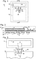
- Figs. 1 through 3 show an exemplary IC package, generally indicated at 10.
- IC package 10 may include a die 12, a transducer 14 providing conversion between electrical and electromagnetic (EM) signals, and conductive connectors 16, such as bond wires 18, 20 electrically connecting the transducer to bond pads 22, 24 connected to a transmitter or receiver circuit included in die 12.
- IC package 10 may further include an encapsulating material 26 formed around at least a portion of the die and/or the transducer. In this example encapsulating material 26 covers die 12, conductive connectors 16, and transducer 14, and is shown in phantom lines so that details of the die and transducer may be illustrated in solid lines.
- Die 12 may include any suitable structure configured as a miniaturized circuit on a suitable die substrate, and is functionally equivalent to a component also referred to as a "chip” or an "integrated circuit (IC)."
- a die substrate may be any suitable semiconductor material; for example, a die substrate may be silicon.
- Die 12 may be mounted with further electrical conductors 16, such as a lead frame, not shown in Figs. 1-3 , providing connection to external circuits.
- An impedance transformer 28, shown in dashed lines, may provide impedance matching between the circuit on die 12 and transducer 14.
- Transducer 14 may be in the form of a folded dipole or loop antenna 30, is configured to operate at radio frequencies in the EHF spectrum, and is configured to transmit and/or receive electromagnetic signals.
- Antenna 30 may be separate from but operatively connected to die 12 by any suitable conductors 16, and may be located adjacent to die 12.
- a loop configuration of antenna 30 may include a 0.1 mm band of material, laid out in a loop 1 .4 mm long and 0.53 mm wide, with a gap of 0.1 mm at the mouth of the loop, and with the edge of the loop approximately 0.2 mm from the edge of die 12.
- Encapsulating material 26 may be used to assist in holding the various components of IC package 10 in fixed relative positions.
- Encapsulating material 26 may be any suitable material configured to provide electrical insulation and physical protection for the electrical and electronic components of IC package 10.
- encapsulating material 26, also referred to as insulating material may be a mold compound, glass, plastic, or ceramic.
- Encapsulating material 26 may be formed in any suitable shape.
- encapsulating material 26 may be in the form of a rectangular block, encapsulating all components of IC package 10 except the unconnected ends of conductors 16 connecting the die to external circuits. External connections may be formed with other circuits or components.
- Fig. 3 shows an exemplary configuration of a transducer 14 connected to die 12 by bond wires 18 and 20 and bond pads 22 and 24.
- the bond wires and bond pads may be configured to limit impedance mismatch between transducer 14 and a circuit of die 12.
- bond wires 18 and 20 may be 0.6 mm long, with an overhead measurement (indicated as dimension "L") of approximately 0.3 mm.
- the bond pads may be approximately 0.066 mm square.
- Bond wires may also be disposed such that they are approximately 0.074 mm apart at a point of attachment to the respective bond pads (indicated as dimension "B") and approximately 0.2 mm apart at a point of attachment to antenna 20 (indicated as dimension "S"). Impedance matching may be further facilitated by use of transformer 28 shown in Fig. 1 .
- IC package 10 may further include a ground plane 32 mounted to the lower surface of die 12 and a package dielectric substrate 34 that may be similar to a dielectric used for PCBs.
- Ground plane 32 may be any suitable structure configured to provide an electrical ground for die 12.
- package ground plane 32 may be a conductive, rectangular, planar structure mounted directly below die 12 on substrate 34.
- Substrate 34 may have two-sided metallization patterns, such as a metallization pattern 36 on the top surface that includes antenna 30, ground plane 32, and conductors connected to die 12 by a suitable set of conductors 16, such as may be provided by a lead frame or flip-chip bumps as discussed further below.
- Package 10 may further include external conductors 38 that connect the package to external circuits, such as are represented by flip-chip solder balls or bumps 40.
- Bumps 40 may be connected to conductors in metallization pattern 36 by ball pads 42 and vias, such as via 44 connecting a bump 46 to ground plane 32.
- Figs. 4 through 6 show other configurations of IC packages.
- Fig. 4 shows an IC package 50 having a die 52, antenna 54, bond wires 56, 58, bond pads 60, 62, impedance transformer 64, and encapsulating material 66, similar to IC package 10.
- antenna 54 is a dipole antenna.
- Figs. 5 and 6 illustrate an IC package 70 having a die 72, a folded dipole antenna 74, impedance transformer 76, and encapsulating material 78, a package dielectric substrate 80, a metallization pattern 82 including antenna 74 and a ground plane 84, package bumps 86, via 88, and ball pads 90 also similar to IC package 10.
- Encapsulating material 78 covers die 72 and antenna 74.
- die 12 is mounted on metallization pattern 82 in a flip chip configuration by flip-chip bumps 92.
- flip chip bumps such as bump 94, connect conductors extending from antenna 74 to corresponding conductor terminals on the underside of die 72, without the use of bond wires.
- Fig. 7 shows yet another alternate embodiment of an IC package 100 having a die 102, a folded dipole antenna 104, encapsulating material 106, a package dielectric substrate 108, a metallization pattern 110 including antenna 104 and a ground plane 112, package bumps 114, via 116, ball pads 118, and flip-chip bumps 120, similar to IC package 70.
- Flip-chip bumps 120 include flip-chip bump 122 that, connects conductors extending from antenna 104 to corresponding conductor terminals on the underside of die 102, which is flip-chip mounted to substrate 108.
- encapsulating material 106 is used primarily as an underfill between die 102 and substrate 108.
- a system for transmitting or receiving signals may include a transducer configured to convert between electrical signals and electromagnetic signals; an integrated circuit (IC) operatively coupled to the transducer, the IC containing at least one of a transmitter circuit that transforms a baseband signal into a radio-frequency signal and conducts the radio-frequency electrical signal to the transducer for transmission as an electromagnetic signal and a receiver circuit that receives from the transducer a radio-frequency electrical signal received as an electromagnetic signal by the transducer and transforms the electromagnetic signal into a baseband signal; and insulating material in which the IC and transducer are at least partly embedded, the insulating material holding the transducer and IC in fixed locations spaced relative to each other.
- IC integrated circuit
- Such a system may further include a dielectric substrate supporting the transducer, IC and insulating material.
- the insulating material may completely cover the transducer.
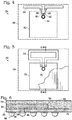
- Fig. 8 shows a representational side view of a communication device 128 including an IC package 130 flip-mounted to an exemplary printed circuit board (PCB) 132.
- IC package 130 includes a die 134, an antenna 136, bond wires, including bond wire 138, connecting the die to the antenna.
- the die, antenna, and bond wires are mounted on a package substrate 140 and encapsulated in encapsulating material 142.
- PCB 132 may include a top dielectric layer 144 having a major face or surface 146.
- IC package 130 is flip-mounted to surface 146 with flip-mounting bumps 148 attached to a metallization pattern (not shown).
- PCB 132 may further include a layer 150 spaced from surface 146 made of conductive material forming a ground plane.
- the PCB ground plane may be any suitable structure configured to provide an electrical ground to circuits and components on PCB 132.
- Ground-plane layer 150 is spaced below antenna 136 by a distance D.
- Distance D may be less than the wavelength of a design frequency depending on the configuration and dimensions of the IC package and PCB.
- PCB ground plane 150 may be located approximately 0.4 mm below mounting surface 146 of PCB 132, and antenna 136 may be mounted in a plane approximately 0.25 mm above mounting surface 146, resulting in a distance D of 0.65 mm between the plane of the antenna and the plane of the ground plane.
- the wavelengths are between 1 cm and 1 mm.
- Fig. 9 shows a simplified exemplary electronic circuit diagram of a transmitter 160 including a transmitter interface circuit 162 and an antenna 164 coupled to the transmit interface circuit.
- the transmit interface circuit may be located on a die, such as die 12 shown in Figs. 1-3 , and may include a transformer 166, a modulator 168, and an amplifier 170.
- transformer 166 is coupled to antenna 164 and receives power on a primary winding from a terminal 172.
- the transformer may provide resonant amplification when combined with a power amplifier, and may provide DC blocking and impedance transformation.
- Modulator 168 may be any suitable modulator, and is illustrated as a pinch device formed of MOSFETs in a cascode configuration that receives an input signal on a terminal 174 used to modulate a carrier signal conducted by amplifier 170.
- Amplifier 170 in this example includes complementary common-source MOSFETs that are driven by a signal applied to terminals 176 and 178 having a selected carrier frequency produced by a voltage-controlled oscillator.
- Fig. 10 shows a simplified diagram of a receiver 180 including a receiver interface circuit 182 and an antenna 184.
- Interface circuit 182 may be included in the integrated circuit in a die, such as die 12 illustrated in Figs. 1-3 .
- a received modulated radio-frequency (RF) signal such as a signal in the EHF band, is conducted through the series connections of transformers and transformer-coupled low-noise amplifiers, including a first transformer 186, amplifier stage 188, a second transformer 190, a second amplifier stage 192, and a third transformer 194.
- Transformers 186, 190 and 194 may receive a DC bias voltage on respective terminals 196, 198, and 200.
- Amplifier power may be applied on associated primary windings of transformers 190 and 194 on respective terminal 202 and 204.
- the amplified and conditioned RF signal is input into a demodulator 206 that converts the received modulated RF signal into a baseband signal.
- the signal output from demodulator 206 may then be fed into a further output comparator 208.
- Comparator 208 also receives an input/output threshold level reference signal from a terminal 210.
- the baseband signal is a binary signal.
- the output from comparator 208 is a logic 1 if the demodulated baseband signal is above the threshold and is a logic 0 if the demodulated baseband signal is below the threshold.
- One or more comparators may also compare an average level of a monitor signal to a predetermined minimum threshold level to determine if a received signal is strong enough to be considered valid. It may be necessary for the receiver antenna to be sufficiently close to a transmitter antenna to communicate a sufficiently strong signal.
- a predetermined minimum threshold level may be set to ensure the electromagnetic signal from a transmitter is considered valid and therefore processed by a receiver if the transmitter antenna and receiver antenna are within a desired physical communication range, such as 5 mm to 10 mm.
- the demodulated baseband signal output from demodulator 206 may be input into a low-pass filter 212 in combination with the input-output reference provided on terminal 210.
- the output of the filter is a monitor signal representative of the average strength of the received demodulated baseband signal, which in turn is representative of the average strength of the received RF signal.
- This average-strength monitor signal is input to a second comparator 214 along with a signal-detect threshold reference signal received on a terminal 216. Comparator 214 thereby monitors the monitor signal output from filter 212 and determines whether the received signal is a sufficiently strong signal.
- the output from comparator 214 is a signal-detect control signal that may have one of two states. In a first state, the control signal indicates that the received signal has sufficient strength to be considered a valid signal. In the second state, the control signal indicates that the received signal does not have sufficient strength.
- the control signal from comparator 214 and the demodulated baseband signal from comparator 208 are input into an AND gate 218. The AND gate then outputs the baseband signal when the control signal is in the first state, indicating that a sufficiently strong signal is being received. If the control signal is in the second state, the AND gate is disabled, and no baseband signal is output from receiver interface circuit 182.
- the signal-detect signal output from comparator 214 may also be output to other circuits on the die or PCB on which the IC is mounted for other uses as appropriate.
- Interface circuit 182 may also have an automatic gain control (AGC) circuit 219.
- AGC circuit 219 may include a third comparator 220 that also receives the output from filter 212 as a signal representative of the average strength of the received signal. Comparator receives as a reference signal an AGC target level signal on a terminal 222. The comparator then produces an output AGC signal that is fed back to amplifier stages 188 and 192 to control the gain of those amplifiers. The AGC circuit maintains a received sufficiently strong signal at a desired level for output by the receiver interface circuit. It will be seen then that the baseband signal input into signal-detect comparator 214 is a conditioned received signal the level of which is modified by amplifier stages 188 and 192 in response to the AGC control signal. If the monitor signal is not sufficiently strong, even with automatic gain control, then AND gate 218 is disabled and no baseband signal is output.
- AGC automatic gain control
- a system includes a first transducer configured to convert electromagnetic signals into electrical signals; and a first IC operatively coupled to the transducer, the IC including a receiver circuit for receiving from the transducer a first radio-frequency electrical signal in an EHF band and transforming the first radio-frequency electrical signal into a first baseband signal, and outputting the first baseband signal when a control signal has a first state and not when the control signal has a second state different than the first state, and a signal-detector circuit responsive to a monitor signal representative of the first baseband for generating the control signal with the first state when the monitor signal indicates the first baseband signal is an acceptable signal and with the second state when the monitor signal indicates the first baseband signal is not an acceptable signal.
- the signal-detector circuit includes a comparator for comparing a characteristic of the monitor signal to a reference, the comparator generating an output signal indicating how the characteristic of the monitor signal compares to the reference, the signal-detector circuit generating the control signal in response to the output signal.
- the characteristic of the monitor signal may be representative of strength of the first baseband signal, and the reference is representative of a threshold signal strength below which reception is disabled and above which reception is enabled.
- the characteristic of the monitor signal may be representative of average signal strength.
- such a system may further include a second transducer configured to convert electrical signals into electromagnetic signals, the second transducer being disposed sufficiently close to the first transducer for the first transducer to receive electromagnetic signals produced by the second transducer; and a second IC operatively coupled to the second transducer, the second IC containing a transmitter circuit for receiving a second baseband signal and transforming the second baseband signal into a second radio-frequency electrical signal and conducting the second radio-frequency electrical signal to the second transducer.
- a method includes receiving by a first transducer a first radio-frequency electromagnetic signal; converting by the first transducer the first radio-frequency electromagnetic signal into a first radio-frequency electrical signal; receiving from the transducer by a receiver circuit of an integrated circuit (IC) the first radio-frequency electrical signal and transforming the first radio-frequency electrical signal into a first baseband signal; generating a monitor signal representative of the first baseband signal; monitoring by a signal-detector circuit the monitor signal; determining whether the monitor signal indicates the first baseband signal is an acceptable signal; generating a control signal with a first state when the monitor signal indicates the first baseband signal is an acceptable signal and with a second state different than the first state when the monitor signal indicates the first baseband signal is not an acceptable signal; outputting by the receiver circuit the first baseband signal when the control signal has the first state; and not outputting by the receiver circuit the first baseband signal when the control signal has the second state.
- IC integrated circuit
- Determining whether the monitor signal indicates the received first radio-frequency electrical signal is an acceptable signal includes comparing a characteristic of the monitor signal to a reference; generating an output signal indicating how the characteristic of the monitor signal compares to the reference; and generating the control signal includes generating the control signal in response to the output signal.
- the characteristic of the monitor signal may be representative of strength of the first baseband signal, and the reference may be representative of a threshold signal strength below which reception is disabled and above which reception is enabled.
- the characteristic of the monitor signal may be representative of average signal strength
- such a method may further include receiving by a second IC containing a transmitter circuit a second baseband signal; transforming the second baseband signal into a second radio-frequency electrical signal; conducting the second radio-frequency electrical signal to a second transducer; positioning the second transducer sufficiently close to the first transducer for the first transducer to receive electromagnetic signals produced by the second transducer; and converting by the second transducer the second radio-frequency electrical signal into the first radio-frequency electromagnetic signal.
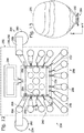
- Figs. 11 and 12 illustrate another exemplary communication device 230 including an IC package 232 with external circuit conductors 234 and 236.
- IC package 232 may include a die 238, a lead frame 240, conductive connectors 242 in the form of bond wires, an antenna 244, encapsulating material 246, and other components not shown to simplify the illustration.
- Die 236 may be mounted in electrical communication with lead frame 240, which may be any suitable arrangement of electrical conductors 248 configured to allow one or more other circuits to operatively connect with die 238.
- Antenna 244 may be constructed as a part of the manufacturing process that produces lead frame 240.
- Leads 248 may be embedded or fixed in a lead frame substrate 250, shown in phantom lines, corresponding to package substrate 34 shown in Fig. 2 .
- the lead frame substrate may be any suitable insulating material configured to substantially hold leads 248 in a predetermined arrangement.
- Electrical communication between die 238 and leads 248 of lead frame 240 may be accomplished by any suitable method using conductive connectors 242.
- conductive connectors 242 may include bond wires that electrically connect terminals on a circuit of die 238 with corresponding conductors 248.
- a conductor 248 may include a plated lead 252 formed on an upper surface of lead frame substrate 250, a via 254 extending through the substrate, a flip-mounting bump 256 mounting IC package 232 to a circuit on a base substrate, such as a PCB, not shown.
- the circuit on the base substrate may include a external conductors, such as external conductor 234, which for example, may include a strip conductor 258 connecting bump 256 to a further via 260 extending through the base substrate.
- Other vias 262 may extend through the lead frame substrate 250 and there may be additional vias 264 extending through the base substrate.
- die 238 may be inverted and conductive connectors 242 may include bumps, or die solder balls, as described previously, which may be configured to electrically connect points on a circuit of die 238 directly to corresponding leads 248 in what is commonly known as a "flip chip" arrangement.
- Lead frame 240 may be configured to create what may be considered a radiation shaper 266 forming effectively a wire mesh backstop for radiation transmitted by antenna 244 or radiation received from an external antenna.
- Other circuit connectors may also contribute to the radiation reflector, including conductive connectors 242, various combinations of external conductors 234 and 236.
- the conductors may conduct active signals or be circuit grounds because electromagnetic signals of sufficiently high frequencies that both types of conductors contribute to the reflections or shaping of the radiation.
- the shaping effect applies to received as well as transmitted radiation. Additionally, various shaping effects are possible, and it may be desirable in some embodiments to have reduced or insubstantial directional shaping effect, essentially creating an electromagnetic signal with omni-directional or hemispherical qualities.
- Lead frame 240 may be configured with conductors 248 separated by a pin pitch or gap, such as distance G shown in Fig. 12 .
- Distance G may be effective if it is significantly less than one wavelength of an operating frequency of the transmitter or receiver.
- the pin pitch may be configured to be 1/10th of the wavelength. This configuration may effectively create a wire mesh, providing a backstop for antenna 244 and directionally shaping an associated electromagnetic signal and directing it substantially away from die 238.
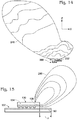
- Figs. 13 and 14 illustrate a characteristic radiation pattern 270 produced by a simulation of an electromagnetic signal emanating from an exemplary transmitting IC package 232 having the radiation shaper 266 described with reference to Figs. 11 and 12 .
- the indicated layers represented in the figures generally corresponds with increasing gain with distance from IC package 232
- the radiation is directed away from die 238 and lead frame 240, shown in Figs. 11 and 12 , in a direction corresponding to the side of die 238 on which antenna 244 is mounted.
- shaping of the electromagnetic signal may be accomplished by the configuration of a ground plane 150 in a PCB 132 of a communication device as described with reference to Fig. 8 , generally deflecting an electromagnetic signal in a direction dependent on the configuration of the PCB ground plane 150 relative to antenna 136 embedded in the right end of IC package 130 as viewed in Figs. 15 and 16 .
- These figures illustrate idealized radiation patterns that may result from different configurations, and are not the results of simulations of these configurations. Actual radiation patterns are dependent on relative configurations, actual structures, and the strength of applied signals.
- ground plane 150 extends out past the antenna in IC package 130 by a distance F that is well beyond the antenna opposite from the position of die 134. It is seen that resulting radiation 280 extends upwardly away from ground plane 150 and away from IC package 130.
- first IC package 130' may be mounted for communication with a second IC package 130".
- Either IC package 10 may be configured to transmit and/or receive electromagnetic signals, providing one- or two-way communication between the two IC packages and any respective accompanying electronic circuits or components that each is connected to.
- First IC package 130' is shown mounted to a first PCB 132' and second IC package 130" is shown mounted to a second PCB 132", whereby the IC packages provide inter-PCB communication.
- first and a second IC packages 130' and 130" may be co-located on a single PCB, such as PCB 132', as indicated by the phantom lines between the PCBs to provide intra-PCB communication.
- First IC package 130' may include a transmitter 160 as described with reference to Fig. 9 .
- second IC package 130" may include a receiver 180 as described with reference to Fig. 10 .
- the appropriate relative positions for IC package 130' and IC package 130" may be determined by operation of the signal detect circuit of receiver interface circuit 182 as described with reference to Fig. 10 .
- a ground plane 150' in PCB 132' may have a leading edge 150A' that is generally in line with the antenna end 130A' of IC package 130'. With the ground plane recessed under IC package 130', it is seen that the radiation 282 extends from end 130A' more to the right in Fig. 16 than the radiation shown in Fig. 15 . The radiation may thereby be directed more toward receiver IC package 130", depending on the actual configuration used. The configuration of a ground plane relative to the antenna may thus also function as a radiation shaper.
- Additional radiation directing may be provided by conductive elements spaced from the antenna, which conductive elements also may function as a radiation shaper.
- An example is shown in Figs. 17 and 18 , which illustrate a communication device 290 including an IC package 292 mounted onto a PCB 294 by package mounting bumps 296.
- PCB extends beyond IC package 292 away from an end 292A of the IC package that contains a die 298 and an antenna 300, as discussed with reference to Figs. 1-3 , for example.
- an array 302 of external director structures, including director structures 304 and 306 are disposed away from IC package end 292A. Arrays with other forms of director structures or more or fewer director structures may be used.
- External director structures 304 and 306 may be any suitable structure configured to passively retransmit electromagnetic radiation.
- External director structures 304 and 306 may be made of any conductive material; for example, copper, aluminum, and/or gold.
- the director structures may be placed at periodic or otherwise spaced intervals from transmitting antenna end 292A of transmitting IC package 292.
- the external director structures may be elongate conductive bars having a length Y approximately 1 mm long and spaced a distance P approximately 1 mm apart, as generally shown in Figs. 17 and 18 .
- radiation 308 transmitted by antenna 300 may energize director structure 304, producing radiation 310.
- Radiation 310 in turn may energize director structure 306, producing radiation 312. Additional director structures may extend the radiation pattern further. It is seen then that a composite elongate radiation pattern 314 may be produced that extends the radiation in an associated direction beyond the radiation that would otherwise be produced by antenna 300 without such director structures.
- Locating an antenna or other transducer off-chip may result in effective antenna impedance matching, independent antenna design, increased transmission power, and selective directional shaping of a resulting radiation pattern.
- the radiation may thus be directed in a direction where a receiving antenna may be positioned.
- Locating an antenna within the package may also provide a customer with a more complete assembly that incorporates characteristics of the assembly to satisfy specifications and tailored operating characteristics, besides protecting an incorporated antenna from damage.
- a system as described above for transmitting or receiving signals may include a transducer configured to convert between radio-frequency electrical signals and radio-frequency electromagnetic signals; an integrated circuit (IC) operatively coupled to the transducer, the IC containing at least one of a transmitter circuit that transforms a baseband signal into a radio-frequency electrical signal and conducts the radio-frequency signal to the transducer and a receiver circuit that receives from the transducer a radio-frequency electrical signal and transforms the radio-frequency electrical signal into a baseband signal; and an electromagnetic-energy directing assembly mounted relative to the transducer for directing electromagnetic energy in a region including the transducer and in a direction away from the IC.
- IC integrated circuit
- the directing assembly includes a lead frame providing external connections to conductors on the IC, and the transducer is configured to convert signals having a predetermined wavelength and the lead frame is spaced from the transducer and includes a plurality of separate conductor elements distributed about the IC and disposed sufficiently close together to reflect electromagnetic energy having the predetermined wavelength. At least a portion of the conductor elements may each be spaced apart from adjacent conductor elements by less than one sixth of the predetermined wavelength.
- the lead frame may reflect electromagnetic energy converted by the transducer predominantly away from the lead frame in a direction associated with the transducer.
- the transducer may be disposed on a first side of the IC on which the lead frame is not disposed.
- the lead frame may be disposed at least along second and third sides of the IC that are each adjacent to the first side.
- the lead frame may be configured to cause received electromagnetic energy to be stronger in a region including the transducer and extending away from the lead frame than in a region including the lead frame and extending away from the transducer.
- a dielectric substrate to which is mounted the IC, lead frame, and transducer, and a printed circuit board (PCB) may have a major face on which the dielectric substrate is mounted.
- the directing assembly further may include a ground plane mounted on the PCB, the ground plane being spaced from and parallel to the major face of the PCB with the transducer spaced from the ground plane.
- the PCB may extend away from the transducer opposite the IC, with the directing assembly including one or more elongate conductive elements disposed in spaced-apart positions on the PCB along a line extending in a direction away from the transducer.
- the one or more conductive elements may each extend transversely of the line.
- the system may further include a dielectric substrate to which are mounted the IC and transducer, and a printed circuit board (PCB) having a major face on which the dielectric substrate is mounted, with the directing assembly further including a ground plane mounted on the PCB in line with the transducer.
- the transducer may be disposed away from the ground plane a preselected distance that is greater than 0.25 mm.
- the ground plane may extend parallel to the major face of the PCB below the IC and terminate at an edge aligned with the transducer, whereby radiation transmitted by the transducer is directed away from the transducer in a direction predominantly away from the IC.
- the ground plane may extend along the IC and transducer and beyond the transducer, whereby radiation transmitted by the transducer is directed away from the ground plane.
- the system may further include a PCB having a major face on which the IC and transducer are mounted.
- the major face of the PCB may extend away from the transducer opposite the IC.
- the directing assembly may include one or more elongate conductive elements disposed in spaced-apart positions on the PCB along a line extending in a direction away from the transducer, the one or more conductive elements each extending transversely of the line.
- the inventions described herein relate to industrial and commercial industries, such as electronics and communications industries using devices that communicate with other devices or devices having communication between components in the devices.
Description
- This disclosure relates to systems and methods related to integrated circuits (ICs)for communication, such as packages having electromagnetic (EM) transducers, such as antennas, embedded with the ICs. The ICs may include signal detector circuits and/or include electromagnetic-energy directing assemblies.
- Advances in semiconductor manufacturing and circuit design technologies have enabled the development and production of ICs with increasingly higher operational frequencies. In turn, electronic products and systems incorporating such integrated circuits are able to provide much greater functionality than previous generations of products. This additional functionality has generally included the processing of increasingly larger amounts of data at increasingly higher speeds.
- Many electronic systems include multiple printed circuit boards (PCBs) upon which these high-speed ICs are mounted, and through which various signals are routed to and from the ICs. In electronic system with at least two PCBs and the need to communicate information between those PCBs, a variety of connector and backplane architectures have been developed to facilitate information flow between the boards. Unfortunately, such connector and backplane architectures introduce a variety of impedance discontinuities into the signal path, resulting in a degradation of signal quality or integrity. Connecting to boards by conventional means, such as signal-carrying mechanical connectors, generally creates discontinuities, requiring expensive electronics to negotiate. Conventional mechanical connectors may also wear out over time, require precise alignment and manufacturing methods, and are susceptible to mechanical jostling.
- These characteristics of conventional connectors can lead to degradation of signal integrity and instability of electronic systems needing to transfer data at very high rates, which in turn limits the utility of such products.
-
US 2008/0238632 A1 discloses an RFID tag wherein an operation control unit sets existence/ nonexistence of a communication distance limitation for reducing a communication distance to a state management unit. If the communication distance limitation is not set, a switch unit is turned ON and a demodulated command is inputted from a command demodulation circuit to a command decode unit. If the communication distance limitation is set, a power intensity monitor unit judges whether the power of a rectification circuit is greater than or equal to a predetermined arbitrary field intensity. If the power is less than the predetermined arbitrary field intensity, the switch unit is turned OFF and various commands demodulated by the command demodulation circuit are not inputted to the command decode unit. - A system according to the present invention is defined in appended
claim 1. - The IC and the transducer may be at least partly embedded in the insulating material and held in fixed locations relative to each other.
- An electromagnetic-energy directing assembly may direct electromagnetic energy in a region including the transducer and in a direction away from the IC.
- In accordance with the present invention, there is also provided a method as defined in claim 5.
-
-
Fig. 1 shows a simplified schematic overhead view of a first example of an Integrated circuit (IC) package including a die and antenna. -
Fig. 2 shows a cross-section of the IC package ofFig. 1 taken along line 2-2. -
Fig. 3 is an enlarged view of an interconnection of the die and antenna ofFigs. 1 and 2 . -
Fig. 4 shows a schematic overhead view of a second example of an IC package including a die and antenna. -
Fig. 5 shows a schematic overhead view of a third example of an IC package including a die and antenna. -
Fig. 6 shows a cross-section of the IC package ofFig. 5 taken along line 6-6. -
Fig. 7 shows another embodiment of an IC package. -
Fig. 8 shows a schematic side view of an exemplary communication device including an IC package and PCB. -
Fig. 9 is a simplified circuit diagram showing portions of an exemplary transmitter circuit and antenna. -
Fig. 10 is a circuit diagram showing portions of an exemplary receiver circuit and antenna. -
Fig. 11 shows an isometric view of another exemplary communication device including an IC package with external circuit conductors. -
Fig. 12 shows a bottom view of the exemplary communication device ofFig. 11 . -
Figs. 13 and14 illustrate a representative radiation pattern resulting from the communication device ofFig. 11 configured as a transmitter. -
Figs. 15 and16 show transmitting devices with two different exemplary configurations of PCB ground planes and stylized representations of resulting radiation patterns. -
Fig. 17 shows an overhead schematic view of an exemplary transmitting device having spaced external director structures. -
Fig. 18 shows a side schematic view of the transmitting device ofFig. 17 , showing a stylized representative radiation pattern. - Wireless communication may be used to provide signal communications between components on a device or may provide communication between devices. Wireless communication provides an interface that is not subject to mechanical and electrical degradation. Examples of systems employing wireless communication between chips are disclosed in
U.S. Patent No. 5,621,913 andU.S. Published Patent Application No. 2010/0159829 . - In one example, tightly-coupled transmitter/receiver pairs may be deployed with a transmitter disposed at a terminal portion of a first conduction path and a receiver disposed at a terminal portion of a second conduction path. The transmitter and receiver may be disposed in close proximity to each other depending on the strength of the transmitted energy, and the first conduction path and the second conduction path may be discontiguous with respect to each other. In exemplary versions, the transmitter and receiver may be disposed on separate circuit carriers positioned with the antennas of the transmitter/receiver pair in close proximity.
- As discussed below, a transmitter or receiver may be configured as an IC package, in which an antenna may be positioned adjacent to a die and held in place by a dielectric or insulating encapsulation or bond material. A transmitter or receiver may be configured as an IC package, in which an antenna may be positioned adjacent to a die and held in place by encapsulation material of the package and/or a lead frame substrate. Examples of EHF antennas embedded in IC packages are shown in the figures and described below.
-
Figs. 1 through 3 show an exemplary IC package, generally indicated at 10. IC package 10 may include a die 12, atransducer 14 providing conversion between electrical and electromagnetic (EM) signals, andconductive connectors 16, such asbond wires bond pads encapsulating material 26 formed around at least a portion of the die and/or the transducer. In thisexample encapsulating material 26 covers die 12,conductive connectors 16, andtransducer 14, and is shown in phantom lines so that details of the die and transducer may be illustrated in solid lines. - Die 12 may include any suitable structure configured as a miniaturized circuit on a suitable die substrate, and is functionally equivalent to a component also referred to as a "chip" or an "integrated circuit (IC)." A die substrate may be any suitable semiconductor material; for example, a die substrate may be silicon. Die 12 may be mounted with further
electrical conductors 16, such as a lead frame, not shown inFigs. 1-3 , providing connection to external circuits. An impedance transformer 28, shown in dashed lines, may provide impedance matching between the circuit on die 12 andtransducer 14. -
Transducer 14 may be in the form of a folded dipole orloop antenna 30, is configured to operate at radio frequencies in the EHF spectrum, and is configured to transmit and/or receive electromagnetic signals.Antenna 30 may be separate from but operatively connected to die 12 by anysuitable conductors 16, and may be located adjacent to die 12. - The dimensions of
antenna 30 are suitable for operation in the EHF band of the electromagnetic frequency spectrum. In one example, a loop configuration ofantenna 30 may include a 0.1 mm band of material, laid out in aloop 1 .4 mm long and 0.53 mm wide, with a gap of 0.1 mm at the mouth of the loop, and with the edge of the loop approximately 0.2 mm from the edge of die 12. - Encapsulating
material 26 may be used to assist in holding the various components of IC package 10 in fixed relative positions. Encapsulatingmaterial 26 may be any suitable material configured to provide electrical insulation and physical protection for the electrical and electronic components of IC package 10. For example, encapsulatingmaterial 26, also referred to as insulating material, may be a mold compound, glass, plastic, or ceramic. Encapsulatingmaterial 26 may be formed in any suitable shape. For example, encapsulatingmaterial 26 may be in the form of a rectangular block, encapsulating all components of IC package 10 except the unconnected ends ofconductors 16 connecting the die to external circuits. External connections may be formed with other circuits or components. -
Fig. 3 shows an exemplary configuration of atransducer 14 connected to die 12 bybond wires bond pads transducer 14 and a circuit ofdie 12. In one exemplary embodiment,bond wires Fig. 1 . - As shown in
Fig. 2 , IC package 10 may further include aground plane 32 mounted to the lower surface ofdie 12 and apackage dielectric substrate 34 that may be similar to a dielectric used for PCBs.Ground plane 32 may be any suitable structure configured to provide an electrical ground fordie 12. For example,package ground plane 32 may be a conductive, rectangular, planar structure mounted directly below die 12 onsubstrate 34.Substrate 34 may have two-sided metallization patterns, such as ametallization pattern 36 on the top surface that includesantenna 30,ground plane 32, and conductors connected to die 12 by a suitable set ofconductors 16, such as may be provided by a lead frame or flip-chip bumps as discussed further below. Package 10 may further includeexternal conductors 38 that connect the package to external circuits, such as are represented by flip-chip solder balls or bumps 40.Bumps 40 may be connected to conductors inmetallization pattern 36 byball pads 42 and vias, such as via 44 connecting a bump 46 toground plane 32. -
Figs. 4 through 6 show other configurations of IC packages.Fig. 4 shows anIC package 50 having a die 52,antenna 54,bond wires 56, 58,bond pads 60, 62,impedance transformer 64, and encapsulatingmaterial 66, similar to IC package 10. However, in this example,antenna 54 is a dipole antenna. -
Figs. 5 and 6 illustrate anIC package 70 having a die 72, a foldeddipole antenna 74, impedance transformer 76, and encapsulatingmaterial 78, apackage dielectric substrate 80, ametallization pattern 82 includingantenna 74 and aground plane 84, package bumps 86, via 88, andball pads 90 also similar to IC package 10. Encapsulatingmaterial 78 covers die 72 andantenna 74. However, in this example, die 12 is mounted onmetallization pattern 82 in a flip chip configuration by flip-chip bumps 92. In particular, flip chip bumps, such asbump 94, connect conductors extending fromantenna 74 to corresponding conductor terminals on the underside ofdie 72, without the use of bond wires. -
Fig. 7 shows yet another alternate embodiment of anIC package 100 having a die 102, a foldeddipole antenna 104, encapsulatingmaterial 106, a package dielectric substrate 108, ametallization pattern 110 includingantenna 104 and a ground plane 112, package bumps 114, via 116,ball pads 118, and flip-chip bumps 120, similar toIC package 70. Flip-chip bumps 120 include flip-chip bump 122 that, connects conductors extending fromantenna 104 to corresponding conductor terminals on the underside ofdie 102, which is flip-chip mounted to substrate 108. In this example, encapsulatingmaterial 106 is used primarily as an underfill betweendie 102 and substrate 108. - It will be appreciated from the above, that a system for transmitting or receiving signals may include a transducer configured to convert between electrical signals and electromagnetic signals; an integrated circuit (IC) operatively coupled to the transducer, the IC containing at least one of a transmitter circuit that transforms a baseband signal into a radio-frequency signal and conducts the radio-frequency electrical signal to the transducer for transmission as an electromagnetic signal and a receiver circuit that receives from the transducer a radio-frequency electrical signal received as an electromagnetic signal by the transducer and transforms the electromagnetic signal into a baseband signal; and insulating material in which the IC and transducer are at least partly embedded, the insulating material holding the transducer and IC in fixed locations spaced relative to each other.
- Such a system may further include a dielectric substrate supporting the transducer, IC and insulating material. The insulating material may completely cover the transducer.
-
Fig. 8 shows a representational side view of acommunication device 128 including anIC package 130 flip-mounted to an exemplary printed circuit board (PCB) 132. In this example, it may be seen thatIC package 130 includes adie 134, anantenna 136, bond wires, includingbond wire 138, connecting the die to the antenna. The die, antenna, and bond wires are mounted on apackage substrate 140 and encapsulated in encapsulatingmaterial 142.PCB 132 may include atop dielectric layer 144 having a major face orsurface 146.IC package 130 is flip-mounted to surface 146 with flip-mountingbumps 148 attached to a metallization pattern (not shown). -
PCB 132 may further include alayer 150 spaced fromsurface 146 made of conductive material forming a ground plane. The PCB ground plane may be any suitable structure configured to provide an electrical ground to circuits and components onPCB 132. Ground-plane layer 150 is spaced belowantenna 136 by a distance D. Distance D may be less than the wavelength of a design frequency depending on the configuration and dimensions of the IC package and PCB. For example,PCB ground plane 150 may be located approximately 0.4 mm below mountingsurface 146 ofPCB 132, andantenna 136 may be mounted in a plane approximately 0.25 mm above mountingsurface 146, resulting in a distance D of 0.65 mm between the plane of the antenna and the plane of the ground plane. Operating in the EHF frequency band between 30 and 300 GHz, the wavelengths are between 1 cm and 1 mm. -
Fig. 9 shows a simplified exemplary electronic circuit diagram of atransmitter 160 including atransmitter interface circuit 162 and anantenna 164 coupled to the transmit interface circuit. The transmit interface circuit may be located on a die, such as die 12 shown inFigs. 1-3 , and may include a transformer 166, amodulator 168, and anamplifier 170. In this example, transformer 166 is coupled toantenna 164 and receives power on a primary winding from a terminal 172. The transformer may provide resonant amplification when combined with a power amplifier, and may provide DC blocking and impedance transformation.Modulator 168 may be any suitable modulator, and is illustrated as a pinch device formed of MOSFETs in a cascode configuration that receives an input signal on a terminal 174 used to modulate a carrier signal conducted byamplifier 170.Amplifier 170 in this example includes complementary common-source MOSFETs that are driven by a signal applied toterminals 176 and 178 having a selected carrier frequency produced by a voltage-controlled oscillator. -
Fig. 10 shows a simplified diagram of areceiver 180 including areceiver interface circuit 182 and anantenna 184.Interface circuit 182 may be included in the integrated circuit in a die, such as die 12 illustrated inFigs. 1-3 . A received modulated radio-frequency (RF) signal, such as a signal in the EHF band, is conducted through the series connections of transformers and transformer-coupled low-noise amplifiers, including afirst transformer 186,amplifier stage 188, asecond transformer 190, asecond amplifier stage 192, and athird transformer 194.Transformers respective terminals transformers respective terminal - The amplified and conditioned RF signal is input into a
demodulator 206 that converts the received modulated RF signal into a baseband signal. The signal output fromdemodulator 206 may then be fed into afurther output comparator 208.Comparator 208 also receives an input/output threshold level reference signal from a terminal 210. In this example, the baseband signal is a binary signal. The output fromcomparator 208 is alogic 1 if the demodulated baseband signal is above the threshold and is a logic 0 if the demodulated baseband signal is below the threshold. - One or more comparators may also compare an average level of a monitor signal to a predetermined minimum threshold level to determine if a received signal is strong enough to be considered valid. It may be necessary for the receiver antenna to be sufficiently close to a transmitter antenna to communicate a sufficiently strong signal. A predetermined minimum threshold level may be set to ensure the electromagnetic signal from a transmitter is considered valid and therefore processed by a receiver if the transmitter antenna and receiver antenna are within a desired physical communication range, such as 5 mm to 10 mm.
- More specifically, the demodulated baseband signal output from
demodulator 206 may be input into a low-pass filter 212 in combination with the input-output reference provided onterminal 210. The output of the filter is a monitor signal representative of the average strength of the received demodulated baseband signal, which in turn is representative of the average strength of the received RF signal. This average-strength monitor signal is input to asecond comparator 214 along with a signal-detect threshold reference signal received on aterminal 216.Comparator 214 thereby monitors the monitor signal output fromfilter 212 and determines whether the received signal is a sufficiently strong signal. - The output from
comparator 214, then, is a signal-detect control signal that may have one of two states. In a first state, the control signal indicates that the received signal has sufficient strength to be considered a valid signal. In the second state, the control signal indicates that the received signal does not have sufficient strength. The control signal fromcomparator 214 and the demodulated baseband signal fromcomparator 208 are input into an ANDgate 218. The AND gate then outputs the baseband signal when the control signal is in the first state, indicating that a sufficiently strong signal is being received. If the control signal is in the second state, the AND gate is disabled, and no baseband signal is output fromreceiver interface circuit 182. The signal-detect signal output fromcomparator 214 may also be output to other circuits on the die or PCB on which the IC is mounted for other uses as appropriate. -
Interface circuit 182 may also have an automatic gain control (AGC)circuit 219.AGC circuit 219 may include athird comparator 220 that also receives the output fromfilter 212 as a signal representative of the average strength of the received signal. Comparator receives as a reference signal an AGC target level signal on a terminal 222. The comparator then produces an output AGC signal that is fed back toamplifier stages comparator 214 is a conditioned received signal the level of which is modified byamplifier stages gate 218 is disabled and no baseband signal is output. - According to the present invention, a system includes a first transducer configured to convert electromagnetic signals into electrical signals; and a first IC operatively coupled to the transducer, the IC including a receiver circuit for receiving from the transducer a first radio-frequency electrical signal in an EHF band and transforming the first radio-frequency electrical signal into a first baseband signal, and outputting the first baseband signal when a control signal has a first state and not when the control signal has a second state different than the first state, and a signal-detector circuit responsive to a monitor signal representative of the first baseband for generating the control signal with the first state when the monitor signal indicates the first baseband signal is an acceptable signal and with the second state when the monitor signal indicates the first baseband signal is not an acceptable signal.
- The signal-detector circuit includes a comparator for comparing a characteristic of the monitor signal to a reference, the comparator generating an output signal indicating how the characteristic of the monitor signal compares to the reference, the signal-detector circuit generating the control signal in response to the output signal. The characteristic of the monitor signal may be representative of strength of the first baseband signal, and the reference is representative of a threshold signal strength below which reception is disabled and above which reception is enabled. The characteristic of the monitor signal may be representative of average signal strength.
- In some examples, such a system may further include a second transducer configured to convert electrical signals into electromagnetic signals, the second transducer being disposed sufficiently close to the first transducer for the first transducer to receive electromagnetic signals produced by the second transducer; and a second IC operatively coupled to the second transducer, the second IC containing a transmitter circuit for receiving a second baseband signal and transforming the second baseband signal into a second radio-frequency electrical signal and conducting the second radio-frequency electrical signal to the second transducer.
- A method according to the present invention includes receiving by a first transducer a first radio-frequency electromagnetic signal; converting by the first transducer the first radio-frequency electromagnetic signal into a first radio-frequency electrical signal; receiving from the transducer by a receiver circuit of an integrated circuit (IC) the first radio-frequency electrical signal and transforming the first radio-frequency electrical signal into a first baseband signal; generating a monitor signal representative of the first baseband signal; monitoring by a signal-detector circuit the monitor signal; determining whether the monitor signal indicates the first baseband signal is an acceptable signal; generating a control signal with a first state when the monitor signal indicates the first baseband signal is an acceptable signal and with a second state different than the first state when the monitor signal indicates the first baseband signal is not an acceptable signal; outputting by the receiver circuit the first baseband signal when the control signal has the first state; and not outputting by the receiver circuit the first baseband signal when the control signal has the second state.
- Determining whether the monitor signal indicates the received first radio-frequency electrical signal is an acceptable signal includes comparing a characteristic of the monitor signal to a reference; generating an output signal indicating how the characteristic of the monitor signal compares to the reference; and generating the control signal includes generating the control signal in response to the output signal. The characteristic of the monitor signal may be representative of strength of the first baseband signal, and the reference may be representative of a threshold signal strength below which reception is disabled and above which reception is enabled. The characteristic of the monitor signal may be representative of average signal strength
- In some examples, such a method may further include receiving by a second IC containing a transmitter circuit a second baseband signal; transforming the second baseband signal into a second radio-frequency electrical signal; conducting the second radio-frequency electrical signal to a second transducer; positioning the second transducer sufficiently close to the first transducer for the first transducer to receive electromagnetic signals produced by the second transducer; and converting by the second transducer the second radio-frequency electrical signal into the first radio-frequency electromagnetic signal.
-
Figs. 11 and12 illustrate anotherexemplary communication device 230 including anIC package 232 withexternal circuit conductors IC package 232 may include adie 238, alead frame 240,conductive connectors 242 in the form of bond wires, anantenna 244, encapsulatingmaterial 246, and other components not shown to simplify the illustration.Die 236 may be mounted in electrical communication withlead frame 240, which may be any suitable arrangement ofelectrical conductors 248 configured to allow one or more other circuits to operatively connect withdie 238.Antenna 244 may be constructed as a part of the manufacturing process that produceslead frame 240. -
Leads 248 may be embedded or fixed in alead frame substrate 250, shown in phantom lines, corresponding to packagesubstrate 34 shown inFig. 2 . The lead frame substrate may be any suitable insulating material configured to substantially hold leads 248 in a predetermined arrangement. Electrical communication betweendie 238 and leads 248 oflead frame 240 may be accomplished by any suitable method usingconductive connectors 242. As mentioned,conductive connectors 242 may include bond wires that electrically connect terminals on a circuit ofdie 238 withcorresponding conductors 248. For example, aconductor 248 may include a platedlead 252 formed on an upper surface oflead frame substrate 250, a via 254 extending through the substrate, a flip-mountingbump 256 mountingIC package 232 to a circuit on a base substrate, such as a PCB, not shown. The circuit on the base substrate may include a external conductors, such asexternal conductor 234, which for example, may include astrip conductor 258 connectingbump 256 to a further via 260 extending through the base substrate.Other vias 262 may extend through thelead frame substrate 250 and there may beadditional vias 264 extending through the base substrate. - In another example, die 238 may be inverted and
conductive connectors 242 may include bumps, or die solder balls, as described previously, which may be configured to electrically connect points on a circuit ofdie 238 directly to correspondingleads 248 in what is commonly known as a "flip chip" arrangement. -
Lead frame 240 may be configured to create what may be considered aradiation shaper 266 forming effectively a wire mesh backstop for radiation transmitted byantenna 244 or radiation received from an external antenna. Other circuit connectors may also contribute to the radiation reflector, includingconductive connectors 242, various combinations ofexternal conductors -
Lead frame 240 may be configured withconductors 248 separated by a pin pitch or gap, such as distance G shown inFig. 12 . Distance G may be effective if it is significantly less than one wavelength of an operating frequency of the transmitter or receiver. For example, the pin pitch may be configured to be 1/10th of the wavelength. This configuration may effectively create a wire mesh, providing a backstop forantenna 244 and directionally shaping an associated electromagnetic signal and directing it substantially away fromdie 238. -
Figs. 13 and14 illustrate acharacteristic radiation pattern 270 produced by a simulation of an electromagnetic signal emanating from an exemplarytransmitting IC package 232 having theradiation shaper 266 described with reference toFigs. 11 and12 . The indicated layers represented in the figures generally corresponds with increasing gain with distance fromIC package 232 As seen by the radiation patterns inFigs. 13 and14 , the radiation is directed away fromdie 238 andlead frame 240, shown inFigs. 11 and12 , in a direction corresponding to the side ofdie 238 on whichantenna 244 is mounted. - Further or alternative shaping of the electromagnetic signal may be accomplished by the configuration of a
ground plane 150 in aPCB 132 of a communication device as described with reference toFig. 8 , generally deflecting an electromagnetic signal in a direction dependent on the configuration of thePCB ground plane 150 relative toantenna 136 embedded in the right end ofIC package 130 as viewed inFigs. 15 and16 . These figures illustrate idealized radiation patterns that may result from different configurations, and are not the results of simulations of these configurations. Actual radiation patterns are dependent on relative configurations, actual structures, and the strength of applied signals. - In the configuration shown in
Fig. 15 ,ground plane 150 extends out past the antenna inIC package 130 by a distance F that is well beyond the antenna opposite from the position ofdie 134. It is seen that resultingradiation 280 extends upwardly away fromground plane 150 and away fromIC package 130. - As shown in
Fig. 16 , first IC package 130' may be mounted for communication with asecond IC package 130". Either IC package 10 may be configured to transmit and/or receive electromagnetic signals, providing one- or two-way communication between the two IC packages and any respective accompanying electronic circuits or components that each is connected to. First IC package 130' is shown mounted to a first PCB 132' andsecond IC package 130" is shown mounted to asecond PCB 132", whereby the IC packages provide inter-PCB communication. In other examples, first and a second IC packages 130' and 130" may be co-located on a single PCB, such as PCB 132', as indicated by the phantom lines between the PCBs to provide intra-PCB communication. - First IC package 130' may include a
transmitter 160 as described with reference toFig. 9 . Correspondingly,second IC package 130" may include areceiver 180 as described with reference toFig. 10 . The appropriate relative positions for IC package 130' andIC package 130" may be determined by operation of the signal detect circuit ofreceiver interface circuit 182 as described with reference toFig. 10 . - Additionally, a ground plane 150' in PCB 132' may have a leading edge 150A' that is generally in line with the
antenna end 130A' of IC package 130'. With the ground plane recessed under IC package 130', it is seen that theradiation 282 extends fromend 130A' more to the right inFig. 16 than the radiation shown inFig. 15 . The radiation may thereby be directed more towardreceiver IC package 130", depending on the actual configuration used. The configuration of a ground plane relative to the antenna may thus also function as a radiation shaper. - Additional radiation directing may be provided by conductive elements spaced from the antenna, which conductive elements also may function as a radiation shaper. An example is shown in
Figs. 17 and 18 , which illustrate acommunication device 290 including anIC package 292 mounted onto aPCB 294 by package mounting bumps 296. PCB extends beyondIC package 292 away from anend 292A of the IC package that contains adie 298 and anantenna 300, as discussed with reference toFigs. 1-3 , for example. In this example, anarray 302 of external director structures, includingdirector structures IC package end 292A. Arrays with other forms of director structures or more or fewer director structures may be used. -
External director structures External director structures antenna end 292A of transmittingIC package 292. For example, the external director structures may be elongate conductive bars having a length Y approximately 1 mm long and spaced a distance P approximately 1 mm apart, as generally shown inFigs. 17 and 18 . In this example, radiation 308 transmitted byantenna 300 may energizedirector structure 304, producingradiation 310.Radiation 310 in turn may energizedirector structure 306, producingradiation 312. Additional director structures may extend the radiation pattern further. It is seen then that a compositeelongate radiation pattern 314 may be produced that extends the radiation in an associated direction beyond the radiation that would otherwise be produced byantenna 300 without such director structures. - It will thus be appreciated that locating an antenna or other transducer off-chip may result in effective antenna impedance matching, independent antenna design, increased transmission power, and selective directional shaping of a resulting radiation pattern. The radiation may thus be directed in a direction where a receiving antenna may be positioned. Locating an antenna within the package may also provide a customer with a more complete assembly that incorporates characteristics of the assembly to satisfy specifications and tailored operating characteristics, besides protecting an incorporated antenna from damage.
- Accordingly, a system as described above for transmitting or receiving signals may include a transducer configured to convert between radio-frequency electrical signals and radio-frequency electromagnetic signals; an integrated circuit (IC) operatively coupled to the transducer, the IC containing at least one of a transmitter circuit that transforms a baseband signal into a radio-frequency electrical signal and conducts the radio-frequency signal to the transducer and a receiver circuit that receives from the transducer a radio-frequency electrical signal and transforms the radio-frequency electrical signal into a baseband signal; and an electromagnetic-energy directing assembly mounted relative to the transducer for directing electromagnetic energy in a region including the transducer and in a direction away from the IC.
- In some examples, the directing assembly includes a lead frame providing external connections to conductors on the IC, and the transducer is configured to convert signals having a predetermined wavelength and the lead frame is spaced from the transducer and includes a plurality of separate conductor elements distributed about the IC and disposed sufficiently close together to reflect electromagnetic energy having the predetermined wavelength. At least a portion of the conductor elements may each be spaced apart from adjacent conductor elements by less than one sixth of the predetermined wavelength. The lead frame may reflect electromagnetic energy converted by the transducer predominantly away from the lead frame in a direction associated with the transducer. The transducer may be disposed on a first side of the IC on which the lead frame is not disposed. The lead frame may be disposed at least along second and third sides of the IC that are each adjacent to the first side. The lead frame may be configured to cause received electromagnetic energy to be stronger in a region including the transducer and extending away from the lead frame than in a region including the lead frame and extending away from the transducer.
- A dielectric substrate to which is mounted the IC, lead frame, and transducer, and a printed circuit board (PCB) may have a major face on which the dielectric substrate is mounted. The directing assembly further may include a ground plane mounted on the PCB, the ground plane being spaced from and parallel to the major face of the PCB with the transducer spaced from the ground plane. The PCB may extend away from the transducer opposite the IC, with the directing assembly including one or more elongate conductive elements disposed in spaced-apart positions on the PCB along a line extending in a direction away from the transducer. The one or more conductive elements may each extend transversely of the line.
- The system may further include a dielectric substrate to which are mounted the IC and transducer, and a printed circuit board (PCB) having a major face on which the dielectric substrate is mounted, with the directing assembly further including a ground plane mounted on the PCB in line with the transducer. The transducer may be disposed away from the ground plane a preselected distance that is greater than 0.25 mm. The ground plane may extend parallel to the major face of the PCB below the IC and terminate at an edge aligned with the transducer, whereby radiation transmitted by the transducer is directed away from the transducer in a direction predominantly away from the IC. The ground plane may extend along the IC and transducer and beyond the transducer, whereby radiation transmitted by the transducer is directed away from the ground plane.
- In some examples, the system may further include a PCB having a major face on which the IC and transducer are mounted. The major face of the PCB may extend away from the transducer opposite the IC. The directing assembly may include one or more elongate conductive elements disposed in spaced-apart positions on the PCB along a line extending in a direction away from the transducer, the one or more conductive elements each extending transversely of the line.
- The inventions described herein relate to industrial and commercial industries, such as electronics and communications industries using devices that communicate with other devices or devices having communication between components in the devices.
- It is believed that the disclosure set forth herein encompasses multiple distinct inventions with independent utility. While each of these inventions has been disclosed in its preferred form, the specific embodiments thereof as disclosed and illustrated herein are not to be considered in a limiting sense as numerous variations are possible. Each example defines an embodiment disclosed in the foregoing disclosure, but any one example does not necessarily encompass all features or combinations that may be eventually claimed. Where the description recites "a" or "a first" element or the equivalent thereof, such description includes one or more such elements, neither requiring nor excluding two or more such elements. Further, ordinal indicators, such as first, second or third, for identified elements are used to distinguish between the elements, and do not indicate a required or limited number of such elements, and do not indicate a particular position or order of such elements unless otherwise specifically stated.
Claims (8)
- A system comprising:a first transducer configured to convert electromagnetic signals into electrical signals; anda first integrated circuit, IC, operatively coupled to the transducer, the IC including:a receiver circuit for receiving from the transducer a first radio- frequency electrical signal in an extremely high frequency, EHF, band and transforming the first radio-frequency electrical signal into a first baseband signal, and outputting the first baseband signal when a control signal has a first state and not when the control signal has a second state different than the first state; anda signal-detector circuit responsive to a monitor signal representative of the first baseband signal for generating the control signal with the first state when the monitor signal indicates the first baseband signal is an acceptable signal and with the second state when the monitor signal indicates the first baseband signal is not an acceptable signalwherein the signal-detector circuit includes a comparator for comparing a characteristic of the monitor signal to a reference, the comparator generating an output signal indicating how the characteristic of the monitor signal compares to the reference, the signal-detector circuit generating the control signal in response to the output signal.
- The system of claim 1, wherein the characteristic of the monitor signal is representative of strength of the first baseband signal, and the reference is representative of a threshold signal strength below which reception is disabled and above which reception is enabled.
- The system of claim 1, wherein the characteristic of the monitor signal is representative of average signal strength of the first baseband signal.
- The system of claim 1, further comprising:a second transducer configured to convert electrical signals into electromagnetic signals, the second transducer being disposed sufficiently close to the first transducer for the first transducer to receive electromagnetic signals produced by the second transducer; anda second IC operatively coupled to the second transducer, the second IC containing a transmitter circuit for receiving a second baseband signal and transforming the second baseband signal into a second radio-frequency electrical signal and conducting the second radio-frequency electrical signal to the second transducer.
- A method comprising:receiving by a first transducer a first radio-frequency electromagnetic signal in an extremely high frequency, EHF, band;converting by the first transducer the first radio-frequency electromagnetic signal into a first radio-frequency electrical signal;receiving from the transducer by a receiver circuit of an integrated circuit, IC, the first radio-frequency electrical signal and transforming the first radio-frequency electrical signal into a first baseband signal;generating a monitor signal representative of the first baseband signal;monitoring by a signal-detector circuit the monitor signal;determining whether the monitor signal indicates the first baseband signal is an acceptable signal, wherein determining whether the monitor signal indicates the first baseband signal is an acceptable signal includes comparing a characteristic of the monitor signal to a reference; generating an output signal indicating how the characteristic of the monitor signal compares to the reference;generating a control signal with a first state when the monitor signal indicates the first baseband signal is an acceptable signal and with a second state different than the first state when the monitor signal indicates the first baseband signal is not an acceptable signal, wherein generating the control signal includes generating the control signal in response to the output signal;outputting by the receiver circuit the first baseband signal when the control signal has the first state; andnot outputting by the receiver circuit the first baseband signal when the control signal has the second state.
- The method of claim 5, wherein the characteristic of the monitor signal is representative of strength of the first baseband signal, and the reference is representative of a threshold signal strength below which reception is disabled and above which reception is enabled.
- The method of claim 6, wherein the characteristic of the monitor signal is representative of average signal strength.
- The method of claim 6, further comprising:receiving by a second IC containing a transmitter circuit a second baseband signal;transforming the second baseband signal into a second radio-frequency electrical signal;conducting the second radio-frequency electrical signal to a second transducer;positioning the second transducer sufficiently close to the first transducer for the first transducer to receive electromagnetic signals produced by the second transducer; andconverting by the second transducer the second radio-frequency electrical signal into the first radio-frequency electromagnetic signal.
Applications Claiming Priority (2)
| Application Number | Priority Date | Filing Date | Title |
|---|---|---|---|
| US201161467334P | 2011-03-24 | 2011-03-24 | |
| PCT/US2012/030166 WO2012129426A2 (en) | 2011-03-24 | 2012-03-22 | Integrated circuit with electromagnetic communication |
Publications (2)
| Publication Number | Publication Date |
|---|---|
| EP2689492A2 EP2689492A2 (en) | 2014-01-29 |
| EP2689492B1 true EP2689492B1 (en) | 2020-01-08 |
Family
ID=45955096
Family Applications (1)
| Application Number | Title | Priority Date | Filing Date |
|---|---|---|---|
| EP12714432.7A Active EP2689492B1 (en) | 2011-03-24 | 2012-03-22 | Integrated circuit with electromagnetic communication |
Country Status (7)
| Country | Link |
|---|---|
| US (2) | US9444146B2 (en) |
| EP (1) | EP2689492B1 (en) |
| JP (2) | JP2014510493A (en) |
| KR (2) | KR101615082B1 (en) |
| CN (1) | CN103563166B (en) |
| TW (2) | TWI631834B (en) |
| WO (1) | WO2012129426A2 (en) |
Families Citing this family (62)
| Publication number | Priority date | Publication date | Assignee | Title |
|---|---|---|---|---|
| US7994622B2 (en) * | 2007-04-16 | 2011-08-09 | Tessera, Inc. | Microelectronic packages having cavities for receiving microelectric elements |
| US8554136B2 (en) * | 2008-12-23 | 2013-10-08 | Waveconnex, Inc. | Tightly-coupled near-field communication-link connector-replacement chips |
| US9954579B2 (en) | 2008-12-23 | 2018-04-24 | Keyssa, Inc. | Smart connectors and associated communications links |
| US9219956B2 (en) | 2008-12-23 | 2015-12-22 | Keyssa, Inc. | Contactless audio adapter, and methods |
| US9474099B2 (en) | 2008-12-23 | 2016-10-18 | Keyssa, Inc. | Smart connectors and associated communications links |
| US9191263B2 (en) | 2008-12-23 | 2015-11-17 | Keyssa, Inc. | Contactless replacement for cabled standards-based interfaces |
| US9960820B2 (en) | 2008-12-23 | 2018-05-01 | Keyssa, Inc. | Contactless data transfer systems and methods |
| TWI429136B (en) * | 2010-04-06 | 2014-03-01 | Univ Nat Taiwan | Stacked antenna structure |
| JP2014510493A (en) | 2011-03-24 | 2014-04-24 | ウェーブコネックス・インコーポレーテッド | Integrated circuit for electromagnetic communication |
| US8714459B2 (en) | 2011-05-12 | 2014-05-06 | Waveconnex, Inc. | Scalable high-bandwidth connectivity |
| US9614590B2 (en) | 2011-05-12 | 2017-04-04 | Keyssa, Inc. | Scalable high-bandwidth connectivity |
| US8811526B2 (en) | 2011-05-31 | 2014-08-19 | Keyssa, Inc. | Delta modulated low power EHF communication link |
| WO2012174350A1 (en) | 2011-06-15 | 2012-12-20 | Waveconnex, Inc. | Proximity sensing and distance measurement using ehf signals |
| JP5844472B2 (en) | 2011-09-15 | 2016-01-20 | ケッサ・インコーポレーテッド | Wireless communication using dielectric media |
| CN104115417A (en) | 2011-10-20 | 2014-10-22 | 基萨公司 | Low-profile wireless connectors |
| TWI633766B (en) | 2011-10-21 | 2018-08-21 | 奇沙公司 | Devices and sysytems for contactless signal splicing |
| EP2792031A1 (en) | 2011-12-14 | 2014-10-22 | Keyssa, Inc. | Connectors providing haptic feedback |
| CN106876373B (en) | 2012-01-30 | 2019-06-14 | 凯萨股份有限公司 | Link radiation control |
| US9559790B2 (en) | 2012-01-30 | 2017-01-31 | Keyssa, Inc. | Link emission control |
| US9344201B2 (en) | 2012-01-30 | 2016-05-17 | Keyssa, Inc. | Shielded EHF connector assemblies |
| KR101578472B1 (en) | 2012-03-02 | 2015-12-17 | 키사, 아이엔씨. | Systems and methods for duplex communication |
| CN106921445A (en) | 2012-03-06 | 2017-07-04 | 凯萨股份有限公司 | System for constraining the operating parameter of EHF communication chips |
| US9553353B2 (en) | 2012-03-28 | 2017-01-24 | Keyssa, Inc. | Redirection of electromagnetic signals using substrate structures |
| WO2013158786A1 (en) | 2012-04-17 | 2013-10-24 | Waveconnex, Inc. | Dielectric lens structures for interchip communication |
| CN104620440B (en) | 2012-08-10 | 2018-02-27 | 凯萨股份有限公司 | Enable EHF display system |
| KR20150041653A (en) | 2012-08-10 | 2015-04-16 | 키사, 아이엔씨. | Dielectric coupling systems for ehf communications |
| US9653927B2 (en) * | 2012-08-10 | 2017-05-16 | Taiwan Semiconductor Manufacturing Company, Ltd. | Composite integrated circuits and methods for wireless interactions therewith |
| US9577314B2 (en) | 2012-09-12 | 2017-02-21 | International Business Machines Corporation | Hybrid on-chip and package antenna |
| WO2014043577A1 (en) | 2012-09-14 | 2014-03-20 | Waveconnex, Inc. | Wireless connections with virtual hysteresis |
| CN104937956B (en) | 2012-12-14 | 2019-05-17 | 凯萨股份有限公司 | Non-contact digital rights management data Transmission system and method |
| EP2932556B1 (en) | 2012-12-17 | 2017-06-07 | Keyssa, Inc. | Modular electronics |
| KR101751386B1 (en) | 2013-03-15 | 2017-06-27 | 키사, 아이엔씨. | Contactless ehf data communication |
| KR101700789B1 (en) | 2013-03-15 | 2017-01-31 | 키사, 아이엔씨. | Extremely high frequency communication chip |
| US9559753B2 (en) * | 2013-03-15 | 2017-01-31 | Keyssa, Inc. | Virtualized physical layer adapted for EHF contactless communication |
| CN105144591B (en) * | 2013-03-15 | 2019-03-08 | 凯萨股份有限公司 | High display system and its operating method |
| WO2014149107A1 (en) | 2013-03-15 | 2014-09-25 | Waveconnex, Inc. | Ehf secure communication device |
| US9407731B2 (en) | 2013-05-16 | 2016-08-02 | Keyssa, Inc. | Extremely high frequency converter |
| WO2015058207A1 (en) | 2013-10-18 | 2015-04-23 | Keyssa, Inc. | Misalignment-tolerant high-density multi-transmitter/receiver modules for extremely-high frequency (ehf) close-proximity wireless connections |
| JP2016005178A (en) * | 2014-06-18 | 2016-01-12 | 株式会社東芝 | Antenna device, information processing apparatus and storage device |
| US10014957B2 (en) * | 2015-03-13 | 2018-07-03 | Texas Instruments Incorporation | High speed isolated and optical USB |
| US9602648B2 (en) | 2015-04-30 | 2017-03-21 | Keyssa Systems, Inc. | Adapter devices for enhancing the functionality of other devices |
| US9940295B2 (en) | 2015-08-14 | 2018-04-10 | Keyssa, Inc. | Extremely high frequency systems and methods of operating the same to establish USB data transport protocols |
| US9640496B2 (en) * | 2015-09-17 | 2017-05-02 | Taiwan Semiconductor Manufacturing Company Ltd. | Semiconductor device |
| US10049801B2 (en) | 2015-10-16 | 2018-08-14 | Keyssa Licensing, Inc. | Communication module alignment |
| WO2017120272A1 (en) * | 2016-01-04 | 2017-07-13 | Infinera Corporation | Photonic integrated circuit package |
| US10250418B2 (en) * | 2016-08-02 | 2019-04-02 | Keyssa Systems, Inc. | EHF receiver architecture with dynamically adjustable discrimination threshold |
| US10454526B1 (en) * | 2017-01-04 | 2019-10-22 | Keyssa Systems, Inc. | Structures for cross-talk reduction |
| US10516207B2 (en) * | 2017-05-17 | 2019-12-24 | Nxp B.V. | High frequency system, communication link |
| US10469112B2 (en) * | 2017-05-31 | 2019-11-05 | Silicon Laboratories Inc. | System, apparatus and method for performing automatic gain control in a receiver for a packet-based protocol |
| KR102058667B1 (en) * | 2017-12-01 | 2019-12-23 | 삼성전기주식회사 | Antenna apparatus and antenna module |
| US11050150B2 (en) | 2017-12-01 | 2021-06-29 | Samsung Electro-Mechanics Co., Ltd. | Antenna apparatus and antenna module |
| CN109873246B (en) * | 2017-12-01 | 2021-06-18 | 三星电机株式会社 | Antenna device and antenna module |
| KR102022354B1 (en) | 2017-12-26 | 2019-09-18 | 삼성전기주식회사 | Antenna module and antenna apparatus |
| US10978796B2 (en) | 2017-12-28 | 2021-04-13 | Samsung Electro-Mechanics Co., Ltd. | Antenna apparatus and antenna module |
| CN110010509B (en) * | 2018-01-05 | 2023-10-20 | 光宝新加坡有限公司 | Double-lead-frame magnetic coupling packaging structure and manufacturing method thereof |
| US11038274B2 (en) | 2018-01-23 | 2021-06-15 | Samsung Electro-Mechanics Co., Ltd. | Antenna apparatus and antenna module |
| KR102035824B1 (en) * | 2018-01-23 | 2019-10-24 | 삼성전기주식회사 | Antenna apparatus and antenna module |
| CN112823504B (en) | 2018-12-17 | 2023-08-11 | Oppo广东移动通信有限公司 | Camera installation module, camera assembly and mobile terminal |
| JP7304166B2 (en) * | 2019-02-13 | 2023-07-06 | パナソニックホールディングス株式会社 | antenna device |
| KR102117459B1 (en) * | 2019-08-29 | 2020-06-01 | 삼성전기주식회사 | Antenna apparatus |
| US11296424B2 (en) * | 2020-01-21 | 2022-04-05 | Rockwell Collins, Inc. | Bump mounted radiating element architecture |
| US20230062415A1 (en) * | 2020-02-05 | 2023-03-02 | Mitsubishi Electric Corporation | Device housing, image reading device, and electrostatic capacitance detection device |
Citations (3)
| Publication number | Priority date | Publication date | Assignee | Title |
|---|---|---|---|---|
| US20070108296A1 (en) * | 2005-11-14 | 2007-05-17 | Konopka John A | Radio frequency identification devices and methods |
| US20080238632A1 (en) * | 2007-03-30 | 2008-10-02 | Takefumi Endo | Semiconductor integrated circuit device |
| US7612674B2 (en) * | 2006-10-27 | 2009-11-03 | Sony Corporation | Radio frequency identification system |
Family Cites Families (286)
| Publication number | Priority date | Publication date | Assignee | Title |
|---|---|---|---|---|
| US2753551A (en) | 1951-06-20 | 1956-07-03 | Raytheon Mfg Co | Circularly polarized radio object locating system |
| DE1081075B (en) | 1956-04-24 | 1960-05-05 | Marie G R P | Dielectric lens |
| US3796831A (en) | 1972-11-13 | 1974-03-12 | Rca Corp | Pulse modulation and detection communications system |
| JPS5410466B2 (en) | 1974-03-01 | 1979-05-07 | ||
| US3971930A (en) | 1974-04-24 | 1976-07-27 | The United States Of America As Represented By The Administrator Of The National Aeronautics And Space Administration | Polarization compensator for optical communications |
| JPS5272502A (en) | 1975-12-13 | 1977-06-17 | Mitsubishi Electric Corp | Code transmitter |
| US4293833A (en) | 1979-11-01 | 1981-10-06 | Hughes Aircraft Company | Millimeter wave transmission line using thallium bromo-iodide fiber |
| JPS57206125A (en) | 1981-06-15 | 1982-12-17 | Toshiba Corp | Hysteresis circuit |
| US4497068A (en) | 1982-01-25 | 1985-01-29 | Eaton Corporation | Encoding system for optic data link |
| JPS58191503A (en) | 1982-05-01 | 1983-11-08 | Junkosha Co Ltd | Transmission line |
| US4678937A (en) | 1984-02-03 | 1987-07-07 | Rosemount Engineering Company Limited | Electrical isolation circuit |
| US4800350A (en) | 1985-05-23 | 1989-01-24 | The United States Of America As Represented By The Secretary Of The Navy | Dielectric waveguide using powdered material |
| US4694504A (en) | 1985-06-03 | 1987-09-15 | Itt Electro Optical Products, A Division Of Itt Corporation | Synchronous, asynchronous, and data rate transparent fiber optic communications link |
| US4771294A (en) | 1986-09-10 | 1988-09-13 | Harris Corporation | Modular interface for monolithic millimeter wave antenna array |
| US4875026A (en) | 1987-08-17 | 1989-10-17 | W. L. Gore & Associates, Inc. | Dielectric waveguide having higher order mode suppression |
| JP2700553B2 (en) | 1988-03-31 | 1998-01-21 | 株式会社 潤工社 | Transmission circuit |
| US4946237A (en) | 1989-06-30 | 1990-08-07 | At&T Bell Laboratories | Cable having non-metallic armoring layer |
| GB9019489D0 (en) | 1990-09-06 | 1990-10-24 | Ncr Co | Antenna control for a wireless local area network station |
| US5199086A (en) | 1991-01-17 | 1993-03-30 | Massachusetts Institute Of Technology | Electro-optic system |
| US5459405A (en) | 1991-05-22 | 1995-10-17 | Wolff Controls Corp. | Method and apparatus for sensing proximity of an object using near-field effects |
| JPH05236031A (en) | 1991-07-23 | 1993-09-10 | Hitachi Maxell Ltd | Data transmission system |
| JPH05327788A (en) | 1992-05-15 | 1993-12-10 | Hitachi Maxell Ltd | Data demodulating circuit |
| US5621913A (en) | 1992-05-15 | 1997-04-15 | Micron Technology, Inc. | System with chip to chip communication |
| JPH076817A (en) | 1993-06-15 | 1995-01-10 | Hitachi Ltd | Connecting device |
| JP3186062B2 (en) | 1994-06-01 | 2001-07-11 | エアーネット・コミュニケイションズ・コーポレイション | Broadband wireless base station utilizing time division multiple access to make a switchable connection to a modulator / demodulator |
| US5471668A (en) | 1994-06-15 | 1995-11-28 | Texas Instruments Incorporated | Combined transmitter/receiver integrated circuit with learn mode |
| DE19512334C1 (en) | 1995-04-01 | 1996-08-29 | Fritsch Klaus Dieter | Electromechanical connection device |
| US5749052A (en) | 1995-05-24 | 1998-05-05 | Tele Digital Development, Inc. | Cellular telephone management system |
| US5543808A (en) | 1995-05-24 | 1996-08-06 | The United States Of America As Represented By The Secretary Of The Army | Dual band EHF, VHF vehicular whip antenna |
| US6351237B1 (en) | 1995-06-08 | 2002-02-26 | Metawave Communications Corporation | Polarization and angular diversity among antenna beams |
| JP3166897B2 (en) | 1995-08-18 | 2001-05-14 | 株式会社村田製作所 | Non-radiative dielectric line and its integrated circuit |
| JPH0983538A (en) | 1995-09-18 | 1997-03-28 | Fujitsu Ltd | I/o card for radio communication and radio communication system by i/o card |
| CN2237914Y (en) | 1995-09-20 | 1996-10-16 | 汪雪松 | Wireless hearing aid |
| SG46955A1 (en) | 1995-10-28 | 1998-03-20 | Inst Of Microelectronics | Ic packaging lead frame for reducing chip stress and deformation |
| US5889449A (en) | 1995-12-07 | 1999-03-30 | Space Systems/Loral, Inc. | Electromagnetic transmission line elements having a boundary between materials of high and low dielectric constants |
| US5943374A (en) | 1995-12-11 | 1999-08-24 | Hitachi Denshi Kabushiki Kaisha | Out-of-synchronization recovery method and apparatus of data transmission system |
| US5754948A (en) | 1995-12-29 | 1998-05-19 | University Of North Carolina At Charlotte | Millimeter-wave wireless interconnection of electronic components |
| US5675349A (en) | 1996-02-12 | 1997-10-07 | Boeing North American, Inc. | Durable, lightweight, radar lens antenna |
| US5894473A (en) | 1996-02-29 | 1999-04-13 | Ericsson Inc. | Multiple access communications system and method using code and time division |
| US5786626A (en) | 1996-03-25 | 1998-07-28 | Ibm Corporation | Thin radio frequency transponder with leadframe antenna structure |
| US5956626A (en) | 1996-06-03 | 1999-09-21 | Motorola, Inc. | Wireless communication device having an electromagnetic wave proximity sensor |
| US6072433A (en) | 1996-07-31 | 2000-06-06 | California Institute Of Technology | Autonomous formation flying sensor |
| CN1178402A (en) | 1996-08-09 | 1998-04-08 | 住友电装株式会社 | Connector for charging electric motor vehicles |
| JPH1065568A (en) | 1996-08-21 | 1998-03-06 | Oki Electric Ind Co Ltd | Radio equipment |
| JP3786497B2 (en) | 1997-06-13 | 2006-06-14 | 富士通株式会社 | Semiconductor module with built-in antenna element |
| JP3269448B2 (en) | 1997-07-11 | 2002-03-25 | 株式会社村田製作所 | Dielectric line |
| CN2313296Y (en) | 1997-07-25 | 1999-04-07 | 电子工业部第五十四研究所 | Eight-multiple diversity receiving simple device for communication signals |
| US5941729A (en) | 1997-09-10 | 1999-08-24 | International Business Machines Corporation | Safe-snap computer cable |
| US6947795B2 (en) | 2001-10-01 | 2005-09-20 | Transoma Medical, Inc. | Frame length modulation and pulse position modulation for telemetry of analog and digital data |
| JP3221382B2 (en) | 1997-12-17 | 2001-10-22 | 株式会社村田製作所 | Non-radiative dielectric line and its integrated circuit |
| JP3889885B2 (en) | 1998-02-27 | 2007-03-07 | シャープ株式会社 | Millimeter-wave transmitter, millimeter-wave receiver, millimeter-wave transmission / reception system, and electronic device |
| JPH11298343A (en) | 1998-04-15 | 1999-10-29 | Sony Corp | Portable communication equipment |
| JP3028804B2 (en) | 1998-07-03 | 2000-04-04 | 日本電気株式会社 | CDMA receiving method and receiving circuit |
| US7548787B2 (en) * | 2005-08-03 | 2009-06-16 | Kamilo Feher | Medical diagnostic and communication system |
| US6590544B1 (en) | 1998-09-01 | 2003-07-08 | Qualcomm, Inc. | Dielectric lens assembly for a feed antenna |
| US6607136B1 (en) | 1998-09-16 | 2003-08-19 | Beepcard Inc. | Physical presence digital authentication system |
| US6492973B1 (en) | 1998-09-28 | 2002-12-10 | Sharp Kabushiki Kaisha | Method of driving a flat display capable of wireless connection and device for driving the same |
| JP3498597B2 (en) | 1998-10-22 | 2004-02-16 | 株式会社村田製作所 | Dielectric line conversion structure, dielectric line device, directional coupler, high frequency circuit module, and transmission / reception device |
| US6373447B1 (en) | 1998-12-28 | 2002-04-16 | Kawasaki Steel Corporation | On-chip antenna, and systems utilizing same |
| US6542720B1 (en) | 1999-03-01 | 2003-04-01 | Micron Technology, Inc. | Microelectronic devices, methods of operating microelectronic devices, and methods of providing microelectronic devices |
| DE19918059C1 (en) | 1999-04-21 | 2000-11-30 | Siemens Ag | Transceiver with bidirectional internal interface lines |
| US6252767B1 (en) | 1999-06-22 | 2001-06-26 | Hewlett-Packard Company | Low impedance hinge for notebook computer |
| AU7346800A (en) | 1999-09-02 | 2001-03-26 | Automated Business Companies | Communication and proximity authorization systems |
| US6590477B1 (en) | 1999-10-29 | 2003-07-08 | Fci Americas Technology, Inc. | Waveguides and backplane systems with at least one mode suppression gap |
| JP3393195B2 (en) | 1999-11-26 | 2003-04-07 | 株式会社ホンダエレシス | Object detection device and occupant detection system |
| US6647246B1 (en) | 2000-01-10 | 2003-11-11 | Industrial Technology Research Institute | Apparatus and method of synchronization using delay measurements |
| JP3932767B2 (en) | 2000-05-12 | 2007-06-20 | 日立電線株式会社 | Array antenna |
| JP2001339207A (en) | 2000-05-26 | 2001-12-07 | Kyocera Corp | Antenna feeding line and antenna module using the same |
| US6741646B1 (en) | 2000-07-25 | 2004-05-25 | Thomson Licensing S.A. | Modulation technique for transmitting a high data rate signal, and an auxiliary data signal, through a band limited channel |
| US6901246B2 (en) | 2000-10-06 | 2005-05-31 | Xg Technology, Llc | Suppressed cycle based carrier modulation using amplitude modulation |
| DE10202480A1 (en) | 2001-01-30 | 2002-08-14 | Infineon Technologies Ag | Signal transfer method for computer, involves converting signal into line-independent electromagnetic wave at transmitter in one electronic module, which is reconverted into reception signal at receiver of other module |
| US7068733B2 (en) | 2001-02-05 | 2006-06-27 | The Directv Group, Inc. | Sampling technique for digital beam former |
| JP2002237036A (en) | 2001-02-08 | 2002-08-23 | Hitachi Ltd | Information recording method, reproducing method and information recorder |
| JP2002261514A (en) | 2001-02-28 | 2002-09-13 | Matsushita Electric Ind Co Ltd | Nrd guide circuit |
| US6512431B2 (en) | 2001-02-28 | 2003-01-28 | Lockheed Martin Corporation | Millimeterwave module compact interconnect |
| JP3530829B2 (en) | 2001-03-12 | 2004-05-24 | 日本ピラー工業株式会社 | Fluororesin composition for electronic parts |
| JP2002312000A (en) | 2001-04-16 | 2002-10-25 | Sakai Yasue | Compression method and device, expansion method and device, compression/expansion system, peak detection method, program, recording medium |
| US7769347B2 (en) | 2001-05-02 | 2010-08-03 | Trex Enterprises Corp. | Wireless communication system |
| US6882239B2 (en) | 2001-05-08 | 2005-04-19 | Formfactor, Inc. | Electromagnetically coupled interconnect system |
| US6967347B2 (en) | 2001-05-21 | 2005-11-22 | The Regents Of The University Of Colorado | Terahertz interconnect system and applications |
| US6534784B2 (en) | 2001-05-21 | 2003-03-18 | The Regents Of The University Of Colorado | Metal-oxide electron tunneling device for solar energy conversion |
| US6531977B2 (en) | 2001-08-03 | 2003-03-11 | Mcewan Technologies, Llc | Pulse center detector for radars and reflectometers |
| US7146139B2 (en) | 2001-09-28 | 2006-12-05 | Siemens Communications, Inc. | System and method for reducing SAR values |
| JP2003218612A (en) | 2001-11-16 | 2003-07-31 | Murata Mfg Co Ltd | Dielectric line, high frequency circuit, and high frequency circuit apparatus |
| JP3852338B2 (en) | 2002-01-15 | 2006-11-29 | 株式会社Kddi研究所 | Method for disconnecting communication link of mobile station in road-to-vehicle communication system |
| JP4523223B2 (en) | 2002-04-26 | 2010-08-11 | 株式会社日立製作所 | Radar sensor |
| US6977551B2 (en) * | 2002-07-19 | 2005-12-20 | Micro Mobio | Dual band power amplifier module for wireless communication devices |
| JP4054634B2 (en) | 2002-08-27 | 2008-02-27 | 沖電気工業株式会社 | Semiconductor device |
| DE10242645A1 (en) | 2002-09-13 | 2004-03-25 | Magcode Ag | Method of creating electrical connection to modules e.g. in motor vehicle, by using magnetic bodies in current providing unit and current receiving unit to form contact automatically |
| US7436876B2 (en) | 2002-11-15 | 2008-10-14 | Time Domain Corporation | System and method for fast acquisition of ultra wideband signals |
| ATE335245T1 (en) | 2002-11-21 | 2006-08-15 | Koninkl Philips Electronics Nv | METHOD FOR DETECTING A GROUP MEMBERSHIP OF TRANSPONDERS |
| JP4514463B2 (en) | 2003-02-12 | 2010-07-28 | パナソニック株式会社 | Transmitting apparatus and wireless communication method |
| US20040176056A1 (en) | 2003-03-07 | 2004-09-09 | Shen Feng | Single-tone detection and adaptive gain control for direct-conversion receivers |
| US7603710B2 (en) | 2003-04-03 | 2009-10-13 | Network Security Technologies, Inc. | Method and system for detecting characteristics of a wireless network |
| US7113087B1 (en) | 2003-04-08 | 2006-09-26 | Microsoft Corporation | Proximity sensing based on antenna impedance variation |
| US7024232B2 (en) | 2003-04-25 | 2006-04-04 | Motorola, Inc. | Wireless communication device with variable antenna radiation pattern and corresponding method |
| US7039397B2 (en) | 2003-07-30 | 2006-05-02 | Lear Corporation | User-assisted programmable appliance control |
| US7228102B2 (en) | 2003-08-05 | 2007-06-05 | Avago Technologie Ecbu Ip (Singapore) Pte. Ltd. | Resonant frequency user proximity detection |
| JP2005117153A (en) | 2003-10-03 | 2005-04-28 | Toshiba Corp | Wireless communication apparatus, wireless communication method, and wireless communication medium |
| JP4133747B2 (en) | 2003-11-07 | 2008-08-13 | 東光株式会社 | Input / output coupling structure of dielectric waveguide |
| US7213766B2 (en) | 2003-11-17 | 2007-05-08 | Dpd Patent Trust Ltd | Multi-interface compact personal token apparatus and methods of use |
| US20050124307A1 (en) | 2003-12-08 | 2005-06-09 | Xytrans, Inc. | Low cost broadband wireless communication system |
| US7761092B2 (en) | 2004-02-06 | 2010-07-20 | Sony Corporation | Systems and methods for communicating with multiple devices |
| WO2005093647A1 (en) | 2004-03-26 | 2005-10-06 | Semiconductor Energy Laboratory Co., Ltd. | Thin semiconductor device and operation method of thin semiconductor device |
| JP4200939B2 (en) | 2004-05-19 | 2008-12-24 | ソニー株式会社 | Wireless communication system, receiving apparatus and receiving method |
| FR2871312B1 (en) | 2004-06-03 | 2006-08-11 | St Microelectronics Sa | CHARGE MODULATION IN AN ELECTROMAGNETIC TRANSPONDER |
| US20060029229A1 (en) | 2004-08-03 | 2006-02-09 | Alexei Trifonov | QKD station with EMI signature suppression |
| US20060082518A1 (en) | 2004-10-19 | 2006-04-20 | Pranil Ram | Multiple monitor display apparatus |
| US8527003B2 (en) | 2004-11-10 | 2013-09-03 | Newlans, Inc. | System and apparatus for high data rate wireless communications |
| US8060102B2 (en) | 2004-12-14 | 2011-11-15 | Bce Inc. | System and method for coverage analysis in a wireless network |
| GB0428046D0 (en) | 2004-12-22 | 2005-01-26 | Artimi Ltd | Contactless connector systems |
| US7787562B2 (en) | 2004-12-29 | 2010-08-31 | Motorola, Inc. | Method and apparatus for adaptive modulation of wireless communication signals |
| US7881675B1 (en) | 2005-01-07 | 2011-02-01 | Gazdzinski Robert F | Wireless connector and methods |
| JP3793822B1 (en) | 2005-01-07 | 2006-07-05 | オプテックス株式会社 | Microwave sensor |
| GB0501593D0 (en) | 2005-01-25 | 2005-03-02 | Innovision Res & Tech Plc | Demodulation apparatus and method |
| US7975079B2 (en) | 2005-02-07 | 2011-07-05 | Broadcom Corporation | Computer chip set having on board wireless interfaces to support parallel communication |
| US8244179B2 (en) | 2005-05-12 | 2012-08-14 | Robin Dua | Wireless inter-device data processing configured through inter-device transmitted data |
| US20060276157A1 (en) | 2005-06-03 | 2006-12-07 | Chen Zhi N | Apparatus and methods for packaging antennas with integrated circuit chips for millimeter wave applications |
| EP1905162A2 (en) | 2005-07-08 | 2008-04-02 | Powercast Corporation | Power transmission system, apparatus and method with communication |
| JP2007036722A (en) | 2005-07-27 | 2007-02-08 | Toshiba Corp | Semiconductor device |
| US7352567B2 (en) | 2005-08-09 | 2008-04-01 | Apple Inc. | Methods and apparatuses for docking a portable electronic device that has a planar like configuration and that operates in multiple orientations |
| US7342299B2 (en) * | 2005-09-21 | 2008-03-11 | International Business Machines Corporation | Apparatus and methods for packaging antennas with integrated circuit chips for millimeter wave applications |
| WO2007038310A1 (en) | 2005-09-23 | 2007-04-05 | California Institute Of Technology | A mm-WAVE FULLY INTEGRATED PHASED ARRAY RECEIVER AND TRANSMITTER WITH ON CHIP ANTENNAS |
| US7311526B2 (en) | 2005-09-26 | 2007-12-25 | Apple Inc. | Magnetic connector for electronic device |
| GB0525635D0 (en) | 2005-12-16 | 2006-01-25 | Innovision Res & Tech Plc | Chip card and method of data communication |
| US20070147425A1 (en) | 2005-12-28 | 2007-06-28 | Wavesat | Wireless modem |
| US7599427B2 (en) | 2005-12-30 | 2009-10-06 | Honeywell International Inc. | Micro range radio frequency (RF) communications link |
| US7512395B2 (en) | 2006-01-31 | 2009-03-31 | International Business Machines Corporation | Receiver and integrated AM-FM/IQ demodulators for gigabit-rate data detection |
| US8014416B2 (en) | 2006-02-14 | 2011-09-06 | Sibeam, Inc. | HD physical layer of a wireless communication device |
| US7664461B2 (en) | 2006-03-02 | 2010-02-16 | Broadcom Corporation | RFID reader architecture |
| US7899394B2 (en) | 2006-03-16 | 2011-03-01 | Broadcom Corporation | RFID system with RF bus |
| US8681810B2 (en) | 2006-04-13 | 2014-03-25 | Qualcomm Incorporated | Dynamic carrier sensing thresholds |
| JP4506722B2 (en) | 2006-05-19 | 2010-07-21 | ソニー株式会社 | Semiconductor element coupling device, semiconductor element, high-frequency module, and semiconductor element coupling method |
| JP4702178B2 (en) | 2006-05-19 | 2011-06-15 | ソニー株式会社 | Semiconductor coupling device, semiconductor element, and high-frequency module |
| US7598923B2 (en) | 2006-05-22 | 2009-10-06 | Sony Corporation | Apparatus and method for communications via multiple millimeter wave signals |
| US7808087B2 (en) | 2006-06-01 | 2010-10-05 | Broadcom Corporation | Leadframe IC packages having top and bottom integrated heat spreaders |
| US7467948B2 (en) | 2006-06-08 | 2008-12-23 | Nokia Corporation | Magnetic connector for mobile electronic devices |
| US7965191B2 (en) | 2006-06-21 | 2011-06-21 | Broadcom Corporation | RFID integrated circuit with integrated antenna structure |
| JP2008022247A (en) | 2006-07-12 | 2008-01-31 | Toshiba Corp | Agc system |
| US8081699B2 (en) | 2006-07-15 | 2011-12-20 | Kazimierz Siwiak | Wireless communication system and method with elliptically polarized radio frequency signals |
| US7936274B2 (en) | 2006-08-30 | 2011-05-03 | Exponent Inc. | Shield for radio frequency ID tag or contactless smart card |
| JP2008083679A (en) | 2006-08-31 | 2008-04-10 | Seiko Epson Corp | Display unit and electronic equipment |
| JP2008079241A (en) | 2006-09-25 | 2008-04-03 | Sharp Corp | Detection circuit, modulation mode discrimination circuit, integrated circuit, tuner device, and multi-system compatible receiver |
| CN101523664B (en) | 2006-10-03 | 2013-06-05 | 碧姆网络有限公司 | Phased shifted oscilator and antenna |
| US8271713B2 (en) | 2006-10-13 | 2012-09-18 | Philips Electronics North America Corporation | Interface systems for portable digital media storage and playback devices |
| US9065682B2 (en) | 2006-11-01 | 2015-06-23 | Silicon Image, Inc. | Wireless HD MAC frame format |
| JP2008124917A (en) | 2006-11-14 | 2008-05-29 | Sony Corp | Radio communications system and radio communications device |
| US20080112101A1 (en) | 2006-11-15 | 2008-05-15 | Mcelwee Patrick T | Transmission line filter for esd protection |
| US8041227B2 (en) | 2006-11-16 | 2011-10-18 | Silicon Laboratories Inc. | Apparatus and method for near-field communication |
| JP2008129919A (en) | 2006-11-22 | 2008-06-05 | Toshiba Corp | Noncontact ic card reader/writer device and control method for output level of transmission radio wave |
| US9697556B2 (en) | 2007-09-06 | 2017-07-04 | Mohammad A. Mazed | System and method of machine learning based user applications |
| US7820990B2 (en) | 2006-12-11 | 2010-10-26 | Lockheed Martin Corporation | System, method and apparatus for RF directed energy |
| GB0700671D0 (en) | 2006-12-15 | 2007-02-21 | Innovision Res & Tech Plc | Nfc communicator and method of data communication |
| US7557303B2 (en) | 2006-12-18 | 2009-07-07 | Lsi Corporation | Electronic component connection support structures including air as a dielectric |
| US8013610B1 (en) | 2006-12-21 | 2011-09-06 | Seektech, Inc. | High-Q self tuning locating transmitter |
| US7460077B2 (en) | 2006-12-21 | 2008-12-02 | Raytheon Company | Polarization control system and method for an antenna array |
| EP1936741A1 (en) | 2006-12-22 | 2008-06-25 | Sony Deutschland GmbH | Flexible substrate integrated waveguides |
| US7557758B2 (en) | 2007-03-26 | 2009-07-07 | Broadcom Corporation | Very high frequency dielectric substrate wave guide |
| US7974587B2 (en) | 2006-12-30 | 2011-07-05 | Broadcom Corporation | Local wireless communications within a device |
| US8350761B2 (en) | 2007-01-04 | 2013-01-08 | Apple Inc. | Antennas for handheld electronic devices |
| US8200156B2 (en) | 2007-01-31 | 2012-06-12 | Broadcom Corporation | Apparatus for allocation of wireless resources |
| US8374157B2 (en) | 2007-02-12 | 2013-02-12 | Wilocity, Ltd. | Wireless docking station |
| JP5034857B2 (en) | 2007-10-12 | 2012-09-26 | ソニー株式会社 | Connector system |
| JP2008252566A (en) | 2007-03-30 | 2008-10-16 | Matsushita Electric Ind Co Ltd | Av equipment |
| US8063769B2 (en) | 2007-03-30 | 2011-11-22 | Broadcom Corporation | Dual band antenna and methods for use therewith |
| US20080290959A1 (en) | 2007-05-22 | 2008-11-27 | Mohammed Ershad Ali | Millimeter wave integrated circuit interconnection scheme |
| US8351982B2 (en) | 2007-05-23 | 2013-01-08 | Broadcom Corporation | Fully integrated RF transceiver integrated circuit |
| US7743659B2 (en) | 2007-05-25 | 2010-06-29 | The Boeing Company | Structural health monitoring (SHM) transducer assembly and system |
| US7722358B2 (en) | 2007-06-15 | 2010-05-25 | Microsoft Corporation | Electrical connection between devices |
| US7929474B2 (en) | 2007-06-22 | 2011-04-19 | Vubiq Incorporated | System and method for wireless communication in a backplane fabric architecture |
| US7768457B2 (en) | 2007-06-22 | 2010-08-03 | Vubiq, Inc. | Integrated antenna and chip package and method of manufacturing thereof |
| US7617342B2 (en) | 2007-06-28 | 2009-11-10 | Broadcom Corporation | Universal serial bus dongle device with wireless telephony transceiver and system for use therewith |
| US7952531B2 (en) * | 2007-07-13 | 2011-05-31 | International Business Machines Corporation | Planar circularly polarized antennas |
| US7830311B2 (en) * | 2007-07-18 | 2010-11-09 | Murata Manufacturing Co., Ltd. | Wireless IC device and electronic device |
| US7941110B2 (en) | 2007-07-23 | 2011-05-10 | Freescale Semiconductor, Inc. | RF circuit with control unit to reduce signal power under appropriate conditions |
| US7908420B2 (en) | 2007-07-31 | 2011-03-15 | Broadcom Corporation | Processing system with millimeter wave host interface and method for use therewith |
| US7825775B2 (en) | 2007-07-31 | 2010-11-02 | Symbol Technologies, Inc. | Antenna-based trigger |
| EP2034623A1 (en) | 2007-09-05 | 2009-03-11 | Nokia Siemens Networks Oy | Adaptive adjustment of an antenna arrangement for exploiting polarization and/or beamforming separation |
| US8965309B2 (en) | 2007-09-18 | 2015-02-24 | Broadcom Corporation | Method and system for calibrating a power amplifier |
| US7881753B2 (en) | 2007-09-28 | 2011-02-01 | Broadcom Corporation | Method and system for sharing multiple antennas between TX and RX in a repeat field of polarization isolation |
| US8244175B2 (en) | 2007-09-28 | 2012-08-14 | Broadcom Corporation | Method and system for signal repeater with gain control and spatial isolation |
| US20090086844A1 (en) | 2007-09-28 | 2009-04-02 | Ahmadreza Rofougaran | Method And System For A Programmable Local Oscillator Generator Utilizing A DDFS For Extremely High Frequencies |
| US8023886B2 (en) | 2007-09-28 | 2011-09-20 | Broadcom Corporation | Method and system for repeater with gain control and isolation via polarization |
| US8634767B2 (en) | 2007-09-30 | 2014-01-21 | Broadcom Corporation | Method and system for utilizing EHF repeaters and/or transceivers for detecting and/or tracking an entity |
| US8856633B2 (en) | 2007-10-03 | 2014-10-07 | Qualcomm Incorporated | Millimeter-wave communications for peripheral devices |
| US7746256B2 (en) | 2007-10-05 | 2010-06-29 | Infineon Technologies Ag | Analog to digital conversion using irregular sampling |
| US8121542B2 (en) | 2007-10-16 | 2012-02-21 | Rafi Zack | Virtual connector based on contactless link |
| US8428528B2 (en) | 2007-10-24 | 2013-04-23 | Biotronik Crm Patent Ag | Radio communications system designed for a low-power receiver |
| US20090153260A1 (en) * | 2007-12-12 | 2009-06-18 | Ahmadreza Rofougaran | Method and system for a configurable transformer integrated on chip |
| US7880677B2 (en) * | 2007-12-12 | 2011-02-01 | Broadcom Corporation | Method and system for a phased array antenna embedded in an integrated circuit package |
| EP2077518B1 (en) | 2008-01-03 | 2013-10-02 | Nxp B.V. | Transponder detection by resonance frequency reduction |
| US7873122B2 (en) | 2008-01-08 | 2011-01-18 | Qualcomm Incorporated | Methods and devices for wireless chip-to-chip communications |
| US9537566B2 (en) | 2008-01-11 | 2017-01-03 | Alcatel-Lucent Usa Inc. | Realizing FDD capability by leveraging existing TDD technology |
| TWI348280B (en) | 2008-01-21 | 2011-09-01 | Univ Nat Taiwan | Dual injection locked frequency dividing circuit |
| US8310444B2 (en) | 2008-01-29 | 2012-11-13 | Pacinian Corporation | Projected field haptic actuation |
| US7750435B2 (en) | 2008-02-27 | 2010-07-06 | Broadcom Corporation | Inductively coupled integrated circuit and methods for use therewith |
| US7795700B2 (en) | 2008-02-28 | 2010-09-14 | Broadcom Corporation | Inductively coupled integrated circuit with magnetic communication path and methods for use therewith |
| US8415777B2 (en) | 2008-02-29 | 2013-04-09 | Broadcom Corporation | Integrated circuit with millimeter wave and inductive coupling and methods for use therewith |
| US8399960B2 (en) | 2008-03-13 | 2013-03-19 | Nec Corporation | Semiconductor device |
| US20090236701A1 (en) | 2008-03-18 | 2009-09-24 | Nanyang Technological University | Chip arrangement and a method of determining an inductivity compensation structure for compensating a bond wire inductivity in a chip arrangement |
| JP4292231B1 (en) | 2008-03-24 | 2009-07-08 | 株式会社東芝 | Electronics |
| JP4497222B2 (en) | 2008-03-26 | 2010-07-07 | ソニー株式会社 | COMMUNICATION DEVICE, COMMUNICATION METHOD, AND COMPUTER PROGRAM |
| JP2009239842A (en) | 2008-03-28 | 2009-10-15 | Renesas Technology Corp | Radio communication system |
| US8269344B2 (en) | 2008-03-28 | 2012-09-18 | Broadcom Corporation | Method and system for inter-chip communication via integrated circuit package waveguides |
| EP2263355B1 (en) | 2008-03-31 | 2012-09-12 | Nxp B.V. | High resolution digital modulator by switching between discrete PWM or PPM values |
| US8184651B2 (en) | 2008-04-09 | 2012-05-22 | Altera Corporation | PLD architecture optimized for 10G Ethernet physical layer solution |
| US20090280765A1 (en) | 2008-05-07 | 2009-11-12 | Ahmadreza Rofougaran | Method And System For On-Demand Filtering In A Receiver |
| US8755849B2 (en) | 2008-05-07 | 2014-06-17 | Broadcom Corporation | Method and system for power management in a beamforming system |
| JP5195911B2 (en) | 2008-06-16 | 2013-05-15 | 日本電気株式会社 | Base station control module, radio base station, base station control device, and base station control method |
| US9300508B2 (en) | 2008-08-07 | 2016-03-29 | Trex Enterprises Corp. | High data rate milllimeter wave radio on a chip |
| US8392965B2 (en) | 2008-09-15 | 2013-03-05 | Oracle International Corporation | Multiple biometric smart card authentication |
| JP2010103982A (en) | 2008-09-25 | 2010-05-06 | Sony Corp | Millimeter wave transmission device, millimeter wave transmission method, and millimeter wave transmission system |
| US8131645B2 (en) | 2008-09-30 | 2012-03-06 | Apple Inc. | System and method for processing media gifts |
| EP2350909A4 (en) | 2008-10-10 | 2013-06-19 | Zapmytv Com Inc | Controlled delivery of content data streams to remote users |
| EP3716673B1 (en) | 2008-10-29 | 2022-09-14 | Marvell Asia Pte, Ltd. | Method and apparatus for performing transmit beamforming sector sweep in a multiantenna communication device |
| US8346234B2 (en) | 2008-11-08 | 2013-01-01 | Absolute Software Corporation | Secure platform management with power savings capacity |
| US8854277B2 (en) | 2008-11-19 | 2014-10-07 | Nxp, B.V. | Millimetre-wave radio antenna module |
| US8324990B2 (en) | 2008-11-26 | 2012-12-04 | Apollo Microwaves, Ltd. | Multi-component waveguide assembly |
| US20100149149A1 (en) | 2008-12-15 | 2010-06-17 | Lawther Joel S | Display system |
| FR2940568A1 (en) | 2008-12-22 | 2010-06-25 | Thomson Licensing | METHOD FOR TRANSMITTING IN A WIRELESS NETWORK AND CORRESPONDING COMMUNICATION MANAGEMENT METHOD |
| US8554136B2 (en) | 2008-12-23 | 2013-10-08 | Waveconnex, Inc. | Tightly-coupled near-field communication-link connector-replacement chips |
| US20100167645A1 (en) | 2008-12-25 | 2010-07-01 | Kabushiki Kaisha Toshiba | Information processing apparatus |
| JP5556072B2 (en) | 2009-01-07 | 2014-07-23 | ソニー株式会社 | Semiconductor device, method of manufacturing the same, and millimeter wave dielectric transmission device |
| TWI384814B (en) | 2009-02-06 | 2013-02-01 | Univ Nat Taiwan | Differential radio frequency signal transmitter and receiver and wireless radio frequency signal transceiver system |
| US8964634B2 (en) | 2009-02-06 | 2015-02-24 | Sony Corporation | Wireless home mesh network bridging adaptor |
| US8326221B2 (en) | 2009-02-09 | 2012-12-04 | Apple Inc. | Portable electronic device with proximity-based content synchronization |
| EP2401825B1 (en) | 2009-02-26 | 2013-12-04 | Battelle Memorial Institute | Submersible vessel data communications system |
| WO2010114079A1 (en) | 2009-03-31 | 2010-10-07 | 京セラ株式会社 | Circuit board, high frequency module, and radar apparatus |
| JP2010245990A (en) | 2009-04-09 | 2010-10-28 | Seiko Epson Corp | Communication method and communication system |
| JP2010256973A (en) | 2009-04-21 | 2010-11-11 | Sony Corp | Information processing device |
| US8179333B2 (en) | 2009-05-08 | 2012-05-15 | Anokiwave, Inc. | Antennas using chip-package interconnections for millimeter-wave wireless communication |
| US8244189B2 (en) | 2009-05-20 | 2012-08-14 | Broadcom Corporation | Method and system for chip-to-chip mesh networks |
| US8346847B2 (en) | 2009-06-03 | 2013-01-01 | Apple Inc. | Installing applications based on a seed application from a separate device |
| US8817891B2 (en) | 2009-06-10 | 2014-08-26 | The Regents Of The University Of California | Milli-meter-wave-wireless-interconnect (M2W2-interconnect) method for short-range communications with ultra-high data rate capability |
| US9007968B2 (en) | 2009-06-16 | 2015-04-14 | Samsung Electronics Co., Ltd. | System and method for wireless multi-band networks association and maintenance |
| US8812833B2 (en) | 2009-06-24 | 2014-08-19 | Marvell World Trade Ltd. | Wireless multiband security |
| JP5278210B2 (en) | 2009-07-13 | 2013-09-04 | ソニー株式会社 | Wireless transmission system, electronic equipment |
| US8427296B2 (en) | 2009-07-14 | 2013-04-23 | Apple Inc. | Method and apparatus for determining the relative positions of connectors |
| US8605826B2 (en) | 2009-08-04 | 2013-12-10 | Georgia Tech Research Corporation | Multi-gigabit millimeter wave receiver system and demodulator system |
| JP5316305B2 (en) | 2009-08-13 | 2013-10-16 | ソニー株式会社 | Wireless transmission system and wireless transmission method |
| JP2011044944A (en) | 2009-08-21 | 2011-03-03 | Sony Corp | Communication device, communication system, and communication method |
| JP2011044953A (en) | 2009-08-21 | 2011-03-03 | Sony Corp | Wired transmission line for av device |
| EP2290391B1 (en) | 2009-09-01 | 2020-12-16 | G4S Monitoring Technologies Limited | Proximity sensors |
| FR2951321B1 (en) | 2009-10-08 | 2012-03-16 | St Microelectronics Sa | SEMICONDUCTOR DEVICE COMPRISING AN ELECTROMAGNETIC WAVEGUIDE |
| EP2309608B1 (en) | 2009-10-09 | 2014-03-19 | Ondal Medical Systems GmbH | Rotatable electrical coupling and connector therefor |
| CN201562854U (en) | 2009-11-25 | 2010-08-25 | 联想(北京)有限公司 | Magnetic connector and electronic device with same |
| US8390249B2 (en) | 2009-11-30 | 2013-03-05 | Broadcom Corporation | Battery with integrated wireless power receiver and/or RFID |
| US8279611B2 (en) | 2009-12-09 | 2012-10-02 | Research In Motion Limited | Flexible cable having rectangular waveguide formed therein and methods of manufacturing same |
| EP2360923A1 (en) | 2010-02-24 | 2011-08-24 | Thomson Licensing | Method for selectively requesting adaptive streaming content and a device implementing the method |
| JP2011176672A (en) | 2010-02-25 | 2011-09-08 | Olympus Corp | Communication conversion device, communication relay system, and communication device |
| JP5665074B2 (en) | 2010-03-19 | 2015-02-04 | シリコンライブラリ株式会社 | Radio transmission system and radio transmitter, radio receiver, radio transmission method, radio reception method, and radio communication method used therefor |
| JP5500679B2 (en) | 2010-03-19 | 2014-05-21 | シリコンライブラリ株式会社 | Radio transmission system and radio transmitter, radio receiver, radio transmission method, radio reception method, and radio communication method used therefor |
| US8781420B2 (en) | 2010-04-13 | 2014-07-15 | Apple Inc. | Adjustable wireless circuitry with antenna-based proximity detector |
| US8774252B2 (en) * | 2010-05-27 | 2014-07-08 | Qualcomm Incorporated | System and method for transmtting and receiving signal with quasi-periodic pulse sequence |
| US8843076B2 (en) | 2010-07-06 | 2014-09-23 | Intel Corporation | Device, system and method of wireless communication over a beamformed communication link |
| US8871565B2 (en) | 2010-09-13 | 2014-10-28 | Semiconductor Energy Laboratory Co., Ltd. | Method for manufacturing semiconductor device |
| KR101288173B1 (en) | 2010-09-17 | 2013-07-18 | 삼성전기주식회사 | Terminal and wireless communication method thereof |
| US8358596B2 (en) | 2010-09-20 | 2013-01-22 | Research In Motion Limited | Communications system providing mobile wireless communications device application module associations for respective wireless communications formats and related methods |
| US9118217B2 (en) | 2010-09-30 | 2015-08-25 | Broadcom Corporation | Portable computing device with wireless power distribution |
| US20120126794A1 (en) | 2010-11-22 | 2012-05-24 | Raymond Jensen | Sensor Assembly And Methods Of Assembling A Sensor Probe |
| EP2461485B1 (en) | 2010-12-01 | 2013-07-31 | Dialog Semiconductor GmbH | A device and method for the transmission and reception of high-fidelity audio using a single wire |
| JP2014510493A (en) | 2011-03-24 | 2014-04-24 | ウェーブコネックス・インコーポレーテッド | Integrated circuit for electromagnetic communication |
| US20120249366A1 (en) | 2011-04-04 | 2012-10-04 | Raytheon Company | Communications on the move antenna system |
| US9141616B2 (en) | 2011-05-06 | 2015-09-22 | Google Inc. | Physical confirmation for network-provided content |
| US9614590B2 (en) | 2011-05-12 | 2017-04-04 | Keyssa, Inc. | Scalable high-bandwidth connectivity |
| TWI620489B (en) | 2011-05-12 | 2018-04-01 | 奇沙公司 | Methods and systems for performing scalable high-bandwidth connectivity using ehf communications, and associated portable devices |
| US8714459B2 (en) | 2011-05-12 | 2014-05-06 | Waveconnex, Inc. | Scalable high-bandwidth connectivity |
| KR20140039009A (en) | 2011-05-31 | 2014-03-31 | 웨이브코넥스, 아이엔씨. | Lta mudulated low power ehf communication link |
| US8811526B2 (en) | 2011-05-31 | 2014-08-19 | Keyssa, Inc. | Delta modulated low power EHF communication link |
| WO2012166502A1 (en) | 2011-06-03 | 2012-12-06 | Marvell World Trade, Ltd. | Method and apparatus for local oscillation distribution |
| WO2012174350A1 (en) | 2011-06-15 | 2012-12-20 | Waveconnex, Inc. | Proximity sensing and distance measurement using ehf signals |
| CN103947126B (en) | 2011-07-05 | 2016-07-06 | 基萨公司 | There is the EHF communication of electric isolution and electrolyte transmission medium |
| US20130278360A1 (en) | 2011-07-05 | 2013-10-24 | Waveconnex, Inc. | Dielectric conduits for ehf communications |
| JP5844472B2 (en) | 2011-09-15 | 2016-01-20 | ケッサ・インコーポレーテッド | Wireless communication using dielectric media |
| CN104115417A (en) | 2011-10-20 | 2014-10-22 | 基萨公司 | Low-profile wireless connectors |
| TWI633766B (en) | 2011-10-21 | 2018-08-21 | 奇沙公司 | Devices and sysytems for contactless signal splicing |
| EP2792031A1 (en) | 2011-12-14 | 2014-10-22 | Keyssa, Inc. | Connectors providing haptic feedback |
| US9559790B2 (en) | 2012-01-30 | 2017-01-31 | Keyssa, Inc. | Link emission control |
| KR101578472B1 (en) | 2012-03-02 | 2015-12-17 | 키사, 아이엔씨. | Systems and methods for duplex communication |
| CN106921445A (en) | 2012-03-06 | 2017-07-04 | 凯萨股份有限公司 | System for constraining the operating parameter of EHF communication chips |
| US9553353B2 (en) | 2012-03-28 | 2017-01-24 | Keyssa, Inc. | Redirection of electromagnetic signals using substrate structures |
| KR20150041653A (en) | 2012-08-10 | 2015-04-16 | 키사, 아이엔씨. | Dielectric coupling systems for ehf communications |
| CN104620440B (en) | 2012-08-10 | 2018-02-27 | 凯萨股份有限公司 | Enable EHF display system |
| US9179490B2 (en) | 2012-11-29 | 2015-11-03 | Intel Corporation | Apparatus, system and method of disconnecting a wireless communication link |
| US9608862B2 (en) | 2013-03-15 | 2017-03-28 | Elwha Llc | Frequency accommodation |
| WO2015058207A1 (en) | 2013-10-18 | 2015-04-23 | Keyssa, Inc. | Misalignment-tolerant high-density multi-transmitter/receiver modules for extremely-high frequency (ehf) close-proximity wireless connections |
-
2012
- 2012-03-22 JP JP2014501249A patent/JP2014510493A/en active Pending
- 2012-03-22 WO PCT/US2012/030166 patent/WO2012129426A2/en active Application Filing
- 2012-03-22 US US13/427,576 patent/US9444146B2/en active Active
- 2012-03-22 EP EP12714432.7A patent/EP2689492B1/en active Active
- 2012-03-22 CN CN201280025060.8A patent/CN103563166B/en active Active
- 2012-03-22 KR KR1020157035915A patent/KR101615082B1/en active IP Right Grant
- 2012-03-22 KR KR1020137027865A patent/KR101582395B1/en active IP Right Grant
- 2012-03-23 TW TW105139861A patent/TWI631834B/en active
- 2012-03-23 TW TW101110057A patent/TWI568200B/en active
-
2015
- 2015-01-14 JP JP2015004839A patent/JP6092269B2/en active Active
- 2015-11-09 US US14/936,411 patent/US9379450B2/en active Active
Patent Citations (3)
| Publication number | Priority date | Publication date | Assignee | Title |
|---|---|---|---|---|
| US20070108296A1 (en) * | 2005-11-14 | 2007-05-17 | Konopka John A | Radio frequency identification devices and methods |
| US7612674B2 (en) * | 2006-10-27 | 2009-11-03 | Sony Corporation | Radio frequency identification system |
| US20080238632A1 (en) * | 2007-03-30 | 2008-10-02 | Takefumi Endo | Semiconductor integrated circuit device |
Also Published As
| Publication number | Publication date |
|---|---|
| JP2014510493A (en) | 2014-04-24 |
| US9444146B2 (en) | 2016-09-13 |
| TW201717552A (en) | 2017-05-16 |
| KR20160003885A (en) | 2016-01-11 |
| JP6092269B2 (en) | 2017-03-08 |
| WO2012129426A2 (en) | 2012-09-27 |
| KR101582395B1 (en) | 2016-01-11 |
| EP2689492A2 (en) | 2014-01-29 |
| TW201244391A (en) | 2012-11-01 |
| CN103563166A (en) | 2014-02-05 |
| US20120263244A1 (en) | 2012-10-18 |
| KR20130141680A (en) | 2013-12-26 |
| WO2012129426A3 (en) | 2012-12-27 |
| TWI568200B (en) | 2017-01-21 |
| TWI631834B (en) | 2018-08-01 |
| KR101615082B1 (en) | 2016-04-29 |
| US9379450B2 (en) | 2016-06-28 |
| CN103563166B (en) | 2019-01-08 |
| US20160064827A1 (en) | 2016-03-03 |
| JP2015092751A (en) | 2015-05-14 |
Similar Documents
| Publication | Publication Date | Title |
|---|---|---|
| EP2689492B1 (en) | Integrated circuit with electromagnetic communication | |
| US10305196B2 (en) | Dielectric lens structures for EHF radiation | |
| US9647715B2 (en) | Contactless signal splicing using an extremely high frequency (EHF) communication link | |
| TWI606778B (en) | Ehf communication with electrical isolation and with dielectric transmission medium | |
| US9705204B2 (en) | Low-profile wireless connectors | |
| US9515859B2 (en) | Delta modulated low-power EHF communication link | |
| US20120086114A1 (en) | Millimeter devices on an integrated circuit | |
| JP5212949B2 (en) | Small variable beam microwave antenna | |
| TW201304438A (en) | Delta modulated low power EHF communication link | |
| TWI557854B (en) | Integrated millimeter-wave chip package |
Legal Events
| Date | Code | Title | Description |
|---|---|---|---|
| PUAI | Public reference made under article 153(3) epc to a published international application that has entered the european phase |
Free format text: ORIGINAL CODE: 0009012 |
|
| 17P | Request for examination filed |
Effective date: 20131017 |
|
| AK | Designated contracting states |
Kind code of ref document: A2 Designated state(s): AL AT BE BG CH CY CZ DE DK EE ES FI FR GB GR HR HU IE IS IT LI LT LU LV MC MK MT NL NO PL PT RO RS SE SI SK SM TR |
|
| DAX | Request for extension of the european patent (deleted) | ||
| RAP1 | Party data changed (applicant data changed or rights of an application transferred) |
Owner name: KEYSSA, INC. |
|
| STAA | Information on the status of an ep patent application or granted ep patent |
Free format text: STATUS: EXAMINATION IS IN PROGRESS |
|
| 17Q | First examination report despatched |
Effective date: 20190410 |
|
| REG | Reference to a national code |
Ref country code: DE Ref legal event code: R079 Ref document number: 602012067083 Country of ref document: DE Free format text: PREVIOUS MAIN CLASS: H01Q0001220000 Ipc: H01L0023660000 |
|
| RIC1 | Information provided on ipc code assigned before grant |
Ipc: H01Q 1/22 20060101ALI20190822BHEP Ipc: H01Q 1/48 20060101ALI20190822BHEP Ipc: H01L 23/66 20060101AFI20190822BHEP Ipc: H01L 23/498 20060101ALN20190822BHEP Ipc: H01Q 7/00 20060101ALI20190822BHEP Ipc: H01L 23/31 20060101ALN20190822BHEP Ipc: H01Q 9/26 20060101ALI20190822BHEP |
|
| GRAP | Despatch of communication of intention to grant a patent |
Free format text: ORIGINAL CODE: EPIDOSNIGR1 |
|
| STAA | Information on the status of an ep patent application or granted ep patent |
Free format text: STATUS: GRANT OF PATENT IS INTENDED |
|
| RIC1 | Information provided on ipc code assigned before grant |
Ipc: H01Q 7/00 20060101ALI20190918BHEP Ipc: H01L 23/66 20060101AFI20190918BHEP Ipc: H01L 23/498 20060101ALN20190918BHEP Ipc: H01L 23/31 20060101ALN20190918BHEP Ipc: H01Q 1/22 20060101ALI20190918BHEP Ipc: H01Q 9/26 20060101ALI20190918BHEP Ipc: H01Q 1/48 20060101ALI20190918BHEP |
|
| INTG | Intention to grant announced |
Effective date: 20191004 |
|
| GRAS | Grant fee paid |
Free format text: ORIGINAL CODE: EPIDOSNIGR3 |
|
| GRAA | (expected) grant |
Free format text: ORIGINAL CODE: 0009210 |
|
| STAA | Information on the status of an ep patent application or granted ep patent |
Free format text: STATUS: THE PATENT HAS BEEN GRANTED |
|
| AK | Designated contracting states |
Kind code of ref document: B1 Designated state(s): AL AT BE BG CH CY CZ DE DK EE ES FI FR GB GR HR HU IE IS IT LI LT LU LV MC MK MT NL NO PL PT RO RS SE SI SK SM TR |
|
| REG | Reference to a national code |
Ref country code: GB Ref legal event code: FG4D |
|
| REG | Reference to a national code |
Ref country code: CH Ref legal event code: EP |
|
| REG | Reference to a national code |
Ref country code: DE Ref legal event code: R096 Ref document number: 602012067083 Country of ref document: DE |
|
| REG | Reference to a national code |
Ref country code: IE Ref legal event code: FG4D |
|
| REG | Reference to a national code |
Ref country code: AT Ref legal event code: REF Ref document number: 1223747 Country of ref document: AT Kind code of ref document: T Effective date: 20200215 |
|
| REG | Reference to a national code |
Ref country code: NL Ref legal event code: MP Effective date: 20200108 |
|
| REG | Reference to a national code |
Ref country code: LT Ref legal event code: MG4D |
|
| PG25 | Lapsed in a contracting state [announced via postgrant information from national office to epo] |
Ref country code: PT Free format text: LAPSE BECAUSE OF FAILURE TO SUBMIT A TRANSLATION OF THE DESCRIPTION OR TO PAY THE FEE WITHIN THE PRESCRIBED TIME-LIMIT Effective date: 20200531 Ref country code: NL Free format text: LAPSE BECAUSE OF FAILURE TO SUBMIT A TRANSLATION OF THE DESCRIPTION OR TO PAY THE FEE WITHIN THE PRESCRIBED TIME-LIMIT Effective date: 20200108 Ref country code: NO Free format text: LAPSE BECAUSE OF FAILURE TO SUBMIT A TRANSLATION OF THE DESCRIPTION OR TO PAY THE FEE WITHIN THE PRESCRIBED TIME-LIMIT Effective date: 20200408 Ref country code: FI Free format text: LAPSE BECAUSE OF FAILURE TO SUBMIT A TRANSLATION OF THE DESCRIPTION OR TO PAY THE FEE WITHIN THE PRESCRIBED TIME-LIMIT Effective date: 20200108 Ref country code: LT Free format text: LAPSE BECAUSE OF FAILURE TO SUBMIT A TRANSLATION OF THE DESCRIPTION OR TO PAY THE FEE WITHIN THE PRESCRIBED TIME-LIMIT Effective date: 20200108 Ref country code: RS Free format text: LAPSE BECAUSE OF FAILURE TO SUBMIT A TRANSLATION OF THE DESCRIPTION OR TO PAY THE FEE WITHIN THE PRESCRIBED TIME-LIMIT Effective date: 20200108 |
|
| PG25 | Lapsed in a contracting state [announced via postgrant information from national office to epo] |
Ref country code: IS Free format text: LAPSE BECAUSE OF FAILURE TO SUBMIT A TRANSLATION OF THE DESCRIPTION OR TO PAY THE FEE WITHIN THE PRESCRIBED TIME-LIMIT Effective date: 20200508 Ref country code: LV Free format text: LAPSE BECAUSE OF FAILURE TO SUBMIT A TRANSLATION OF THE DESCRIPTION OR TO PAY THE FEE WITHIN THE PRESCRIBED TIME-LIMIT Effective date: 20200108 Ref country code: SE Free format text: LAPSE BECAUSE OF FAILURE TO SUBMIT A TRANSLATION OF THE DESCRIPTION OR TO PAY THE FEE WITHIN THE PRESCRIBED TIME-LIMIT Effective date: 20200108 Ref country code: HR Free format text: LAPSE BECAUSE OF FAILURE TO SUBMIT A TRANSLATION OF THE DESCRIPTION OR TO PAY THE FEE WITHIN THE PRESCRIBED TIME-LIMIT Effective date: 20200108 Ref country code: GR Free format text: LAPSE BECAUSE OF FAILURE TO SUBMIT A TRANSLATION OF THE DESCRIPTION OR TO PAY THE FEE WITHIN THE PRESCRIBED TIME-LIMIT Effective date: 20200409 Ref country code: BG Free format text: LAPSE BECAUSE OF FAILURE TO SUBMIT A TRANSLATION OF THE DESCRIPTION OR TO PAY THE FEE WITHIN THE PRESCRIBED TIME-LIMIT Effective date: 20200408 |
|
| REG | Reference to a national code |
Ref country code: DE Ref legal event code: R097 Ref document number: 602012067083 Country of ref document: DE |
|
| PG25 | Lapsed in a contracting state [announced via postgrant information from national office to epo] |
Ref country code: SM Free format text: LAPSE BECAUSE OF FAILURE TO SUBMIT A TRANSLATION OF THE DESCRIPTION OR TO PAY THE FEE WITHIN THE PRESCRIBED TIME-LIMIT Effective date: 20200108 Ref country code: EE Free format text: LAPSE BECAUSE OF FAILURE TO SUBMIT A TRANSLATION OF THE DESCRIPTION OR TO PAY THE FEE WITHIN THE PRESCRIBED TIME-LIMIT Effective date: 20200108 Ref country code: SK Free format text: LAPSE BECAUSE OF FAILURE TO SUBMIT A TRANSLATION OF THE DESCRIPTION OR TO PAY THE FEE WITHIN THE PRESCRIBED TIME-LIMIT Effective date: 20200108 Ref country code: RO Free format text: LAPSE BECAUSE OF FAILURE TO SUBMIT A TRANSLATION OF THE DESCRIPTION OR TO PAY THE FEE WITHIN THE PRESCRIBED TIME-LIMIT Effective date: 20200108 Ref country code: CZ Free format text: LAPSE BECAUSE OF FAILURE TO SUBMIT A TRANSLATION OF THE DESCRIPTION OR TO PAY THE FEE WITHIN THE PRESCRIBED TIME-LIMIT Effective date: 20200108 Ref country code: ES Free format text: LAPSE BECAUSE OF FAILURE TO SUBMIT A TRANSLATION OF THE DESCRIPTION OR TO PAY THE FEE WITHIN THE PRESCRIBED TIME-LIMIT Effective date: 20200108 Ref country code: MC Free format text: LAPSE BECAUSE OF FAILURE TO SUBMIT A TRANSLATION OF THE DESCRIPTION OR TO PAY THE FEE WITHIN THE PRESCRIBED TIME-LIMIT Effective date: 20200108 Ref country code: DK Free format text: LAPSE BECAUSE OF FAILURE TO SUBMIT A TRANSLATION OF THE DESCRIPTION OR TO PAY THE FEE WITHIN THE PRESCRIBED TIME-LIMIT Effective date: 20200108 |
|
| REG | Reference to a national code |
Ref country code: CH Ref legal event code: PL |
|
| PLBE | No opposition filed within time limit |
Free format text: ORIGINAL CODE: 0009261 |
|
| STAA | Information on the status of an ep patent application or granted ep patent |
Free format text: STATUS: NO OPPOSITION FILED WITHIN TIME LIMIT |
|
| REG | Reference to a national code |
Ref country code: AT Ref legal event code: MK05 Ref document number: 1223747 Country of ref document: AT Kind code of ref document: T Effective date: 20200108 |
|
| 26N | No opposition filed |
Effective date: 20201009 |
|
| REG | Reference to a national code |
Ref country code: BE Ref legal event code: MM Effective date: 20200331 |
|
| PG25 | Lapsed in a contracting state [announced via postgrant information from national office to epo] |
Ref country code: LU Free format text: LAPSE BECAUSE OF NON-PAYMENT OF DUE FEES Effective date: 20200322 |
|
| PG25 | Lapsed in a contracting state [announced via postgrant information from national office to epo] |
Ref country code: FR Free format text: LAPSE BECAUSE OF NON-PAYMENT OF DUE FEES Effective date: 20200331 Ref country code: IE Free format text: LAPSE BECAUSE OF NON-PAYMENT OF DUE FEES Effective date: 20200322 Ref country code: LI Free format text: LAPSE BECAUSE OF NON-PAYMENT OF DUE FEES Effective date: 20200331 Ref country code: CH Free format text: LAPSE BECAUSE OF NON-PAYMENT OF DUE FEES Effective date: 20200331 Ref country code: IT Free format text: LAPSE BECAUSE OF FAILURE TO SUBMIT A TRANSLATION OF THE DESCRIPTION OR TO PAY THE FEE WITHIN THE PRESCRIBED TIME-LIMIT Effective date: 20200108 Ref country code: AT Free format text: LAPSE BECAUSE OF FAILURE TO SUBMIT A TRANSLATION OF THE DESCRIPTION OR TO PAY THE FEE WITHIN THE PRESCRIBED TIME-LIMIT Effective date: 20200108 |
|
| PG25 | Lapsed in a contracting state [announced via postgrant information from national office to epo] |
Ref country code: SI Free format text: LAPSE BECAUSE OF FAILURE TO SUBMIT A TRANSLATION OF THE DESCRIPTION OR TO PAY THE FEE WITHIN THE PRESCRIBED TIME-LIMIT Effective date: 20200108 Ref country code: BE Free format text: LAPSE BECAUSE OF NON-PAYMENT OF DUE FEES Effective date: 20200331 Ref country code: PL Free format text: LAPSE BECAUSE OF FAILURE TO SUBMIT A TRANSLATION OF THE DESCRIPTION OR TO PAY THE FEE WITHIN THE PRESCRIBED TIME-LIMIT Effective date: 20200108 |
|
| PG25 | Lapsed in a contracting state [announced via postgrant information from national office to epo] |
Ref country code: TR Free format text: LAPSE BECAUSE OF FAILURE TO SUBMIT A TRANSLATION OF THE DESCRIPTION OR TO PAY THE FEE WITHIN THE PRESCRIBED TIME-LIMIT Effective date: 20200108 Ref country code: MT Free format text: LAPSE BECAUSE OF FAILURE TO SUBMIT A TRANSLATION OF THE DESCRIPTION OR TO PAY THE FEE WITHIN THE PRESCRIBED TIME-LIMIT Effective date: 20200108 Ref country code: CY Free format text: LAPSE BECAUSE OF FAILURE TO SUBMIT A TRANSLATION OF THE DESCRIPTION OR TO PAY THE FEE WITHIN THE PRESCRIBED TIME-LIMIT Effective date: 20200108 |
|
| PG25 | Lapsed in a contracting state [announced via postgrant information from national office to epo] |
Ref country code: MK Free format text: LAPSE BECAUSE OF FAILURE TO SUBMIT A TRANSLATION OF THE DESCRIPTION OR TO PAY THE FEE WITHIN THE PRESCRIBED TIME-LIMIT Effective date: 20200108 Ref country code: AL Free format text: LAPSE BECAUSE OF FAILURE TO SUBMIT A TRANSLATION OF THE DESCRIPTION OR TO PAY THE FEE WITHIN THE PRESCRIBED TIME-LIMIT Effective date: 20200108 |
|
| REG | Reference to a national code |
Ref country code: GB Ref legal event code: 732E Free format text: REGISTERED BETWEEN 20220609 AND 20220615 |
|
| REG | Reference to a national code |
Ref country code: DE Ref legal event code: R082 Ref document number: 602012067083 Country of ref document: DE Representative=s name: TER MEER STEINMEISTER & PARTNER PATENTANWAELTE, DE |
|
| REG | Reference to a national code |
Ref country code: DE Ref legal event code: R081 Ref document number: 602012067083 Country of ref document: DE Owner name: MOLEX, LLC, LISLE, US Free format text: FORMER OWNER: KEYSSA, INC., MOUNTAIN VIEW, CA, US |
|
| PGFP | Annual fee paid to national office [announced via postgrant information from national office to epo] |
Ref country code: GB Payment date: 20230126 Year of fee payment: 12 Ref country code: DE Payment date: 20230125 Year of fee payment: 12 |
|
| P01 | Opt-out of the competence of the unified patent court (upc) registered |
Effective date: 20230528 |