JP2008070874A - Apparatus and method for making flexible display - Google Patents
Apparatus and method for making flexible display Download PDFInfo
- Publication number
- JP2008070874A JP2008070874A JP2007234959A JP2007234959A JP2008070874A JP 2008070874 A JP2008070874 A JP 2008070874A JP 2007234959 A JP2007234959 A JP 2007234959A JP 2007234959 A JP2007234959 A JP 2007234959A JP 2008070874 A JP2008070874 A JP 2008070874A
- Authority
- JP
- Japan
- Prior art keywords
- display device
- manufacturing
- flexible display
- flexible
- support body
- Prior art date
- Legal status (The legal status is an assumption and is not a legal conclusion. Google has not performed a legal analysis and makes no representation as to the accuracy of the status listed.)
- Pending
Links
Images


Classifications
-
- H—ELECTRICITY
- H05—ELECTRIC TECHNIQUES NOT OTHERWISE PROVIDED FOR
- H05B—ELECTRIC HEATING; ELECTRIC LIGHT SOURCES NOT OTHERWISE PROVIDED FOR; CIRCUIT ARRANGEMENTS FOR ELECTRIC LIGHT SOURCES, IN GENERAL
- H05B33/00—Electroluminescent light sources
- H05B33/10—Apparatus or processes specially adapted to the manufacture of electroluminescent light sources
-
- G—PHYSICS
- G02—OPTICS
- G02F—OPTICAL DEVICES OR ARRANGEMENTS FOR THE CONTROL OF LIGHT BY MODIFICATION OF THE OPTICAL PROPERTIES OF THE MEDIA OF THE ELEMENTS INVOLVED THEREIN; NON-LINEAR OPTICS; FREQUENCY-CHANGING OF LIGHT; OPTICAL LOGIC ELEMENTS; OPTICAL ANALOGUE/DIGITAL CONVERTERS
- G02F1/00—Devices or arrangements for the control of the intensity, colour, phase, polarisation or direction of light arriving from an independent light source, e.g. switching, gating or modulating; Non-linear optics
- G02F1/01—Devices or arrangements for the control of the intensity, colour, phase, polarisation or direction of light arriving from an independent light source, e.g. switching, gating or modulating; Non-linear optics for the control of the intensity, phase, polarisation or colour
- G02F1/13—Devices or arrangements for the control of the intensity, colour, phase, polarisation or direction of light arriving from an independent light source, e.g. switching, gating or modulating; Non-linear optics for the control of the intensity, phase, polarisation or colour based on liquid crystals, e.g. single liquid crystal display cells
- G02F1/133—Constructional arrangements; Operation of liquid crystal cells; Circuit arrangements
- G02F1/1333—Constructional arrangements; Manufacturing methods
- G02F1/133305—Flexible substrates, e.g. plastics, organic film
Abstract
Description
本発明は、可撓性表示装置の製造装置及び製造方法に関する。 The present invention relates to a manufacturing apparatus and a manufacturing method for a flexible display device.
現在広く使用されている平板表示装置の代表格が、液晶表示装置及び有機発光表示装置である。
液晶表示装置は、現在最も広く使用されている平板表示装置のうちの1つであって、画素電極及び共通電極などの電場生成電極が形成されている2枚の表示板、及びこれらの間に形成されている液晶層からなって、電場生成電極に電圧を印加して液晶層に電場を生成し、これによって液晶層の液晶分子の配向を決定して入射光の偏光を制御することによって画像を表示する、表示装置である。
Typical examples of flat display devices that are widely used at present are liquid crystal display devices and organic light emitting display devices.
The liquid crystal display device is one of the most widely used flat panel display devices, two display plates on which electric field generating electrodes such as a pixel electrode and a common electrode are formed, and a gap between them. An image is formed by forming a liquid crystal layer and applying an electric voltage to an electric field generating electrode to generate an electric field in the liquid crystal layer, thereby determining the orientation of liquid crystal molecules in the liquid crystal layer and controlling the polarization of incident light. Is a display device.
有機発光表示装置は、正孔注入電極(アノード)及び電子注入電極(カソード)、及びこれらの間に形成されている有機発光層からなって、アノードから注入される正孔及びカソードから注入される電子が有機発光層で再結合して消滅して光を放出する、自己発光型表示装置である。
しかし、これらの表示装置は、重量が重くて破損しやすいガラス基板を使用するため、携帯性及び大画面の表示に限界がある。したがって、最近では、重量が軽くて衝撃に強く、可撓性(flexible)のプラスチック基板を使用する表示装置が開発されている。
The organic light emitting display device includes a hole injection electrode (anode), an electron injection electrode (cathode), and an organic light emitting layer formed therebetween, and is injected from the anode and cathode. A self-luminous display device in which electrons recombine in an organic light emitting layer and disappear to emit light.
However, since these display devices use a glass substrate that is heavy and easily damaged, there is a limit to portability and display on a large screen. Therefore, recently, a display device has been developed that uses a flexible plastic substrate that is light in weight, resistant to impact, and flexible.
ところが、 可撓性のプラスチック基板は、熱を加えると曲がったり膨張する性質があるため、その上に電極や信号線などの薄膜パターンを正確に形成するのが難しい。これを解決するために、可撓性のプラスチック基板をガラス支持体に接着させた状態で薄膜パターンを形成した後、プラスチック基板をガラス支持体から分離する方法が提示された。このような方法は、プラスチック基板を接着剤を利用してガラス支持体に接着する。
しかし、接着剤を利用してプラスチック基板を接着して固定する場合、接着剤による不良が発生する恐れがある。そのため、安定的に工程を進めることができない。
本発明が目的とする技術的課題は、可撓性表示装置を製造する際に、可撓性基板のベンド現象を防止して、安定的に工程を進めることにある。
However, when the plastic substrate is bonded and fixed using an adhesive, there is a possibility that a defect due to the adhesive may occur. Therefore, the process cannot be stably performed.
A technical problem to be solved by the present invention is to prevent a bend phenomenon of a flexible substrate and to proceed a process stably when manufacturing a flexible display device.
本発明1による可撓性表示装置の製造装置は、支持体本体、前記支持体本体の表面に位置し、複数の溝が形成されていて、可撓性母基板を据置く据置台、前記支持体本体を貫通して前記溝と連通していて、一側端が外部と連通している真空路、そして前記真空路及び外部を連通させるニップル部を含む。
ニップル部に例えば真空吸着装置を連結して、真空路の内部及び真空路と連結されている溝を真空状態にして、可撓性母基板を支持体本体の据置台に付着させる。この状態で可撓性母基板上に薄膜パターンを形成する。この時、可撓性母基板は、支持体本体に堅固に固定されているので、曲がったり膨張しない。また、支持体及び可撓性母基板の間に接着剤が使用されていないので、接着剤による不良を防止することができる。
The manufacturing apparatus for a flexible display device according to the first aspect of the present invention includes a support body, a table that is located on a surface of the support body, has a plurality of grooves, and on which a flexible mother board is placed, the support A vacuum path that penetrates through the body body and communicates with the groove and has one end communicating with the outside, and a nipple portion that communicates the vacuum path and the exterior.
For example, a vacuum suction device is connected to the nipple portion, the inside of the vacuum path and the groove connected to the vacuum path are evacuated, and the flexible mother substrate is attached to the mounting base of the support body. In this state, a thin film pattern is formed on the flexible mother substrate. At this time, since the flexible mother board is firmly fixed to the support body, it does not bend or expand. In addition, since no adhesive is used between the support and the flexible mother substrate, defects due to the adhesive can be prevented.
発明2は、発明1において、前記ニップル部の入口に回動可能に付着されて、選択的に開閉動作する栓をさらに含む。
例えば、ニップル部に真空吸着装置に連結されたコネクタの連結管を接続する際に、ニップル部の入口をふさいでいた栓が上に回動する。したがって、コネクタを通じて真空吸着装置及び真空路が連通する。そして、真空路を真空状態にした後、ニップル部から連結管を外すと、ニップル部の栓は再び下に回動して、ニップル部の入口がふさがれる。したがって、真空路及び溝の内部の真空状態が安定的に維持される。
A second aspect of the present invention further includes a plug that is pivotally attached to the inlet of the nipple portion and selectively opens and closes.
For example, when connecting the connecting pipe of the connector connected to the vacuum suction device to the nipple portion, the stopper that blocked the inlet of the nipple portion rotates upward. Therefore, the vacuum suction device and the vacuum path communicate with each other through the connector. Then, after the vacuum path is evacuated, when the connecting pipe is removed from the nipple portion, the plug of the nipple portion rotates downward again and the inlet of the nipple portion is blocked. Therefore, the vacuum state inside the vacuum path and the groove is stably maintained.
発明3は、発明1において、前記支持体本体を固定するガイド部をさらに含む。
発明4は、発明3において、外部の真空吸着装置と連結されていて、前記ニップル部と脱着可能なコネクタをさらに含む。
発明5は、発明4において、前記コネクタは、前記ガイド部上にスライド移動するように付着されている。
The invention 3 further includes a guide portion for fixing the support body in the
A fourth aspect of the present invention further includes a connector that is connected to an external vacuum suction device and is detachable from the nipple portion.
A fifth aspect of the invention is the invention according to the fourth aspect, wherein the connector is attached so as to slide on the guide portion.
発明6は、発明3において、前記ガイド部に前記支持体本体を固定する複数の固定ピンをさらに含む。
発明7は、発明1において、前記溝は断面がV字型である。
発明8は、発明1において、前記溝は平面が格子形状である。
発明9は、発明1において、前記支持体本体はアルミニウムを含む。
A sixth aspect of the present invention according to the third aspect further includes a plurality of fixing pins for fixing the support body to the guide portion.
The invention 7 is the
The invention 8 is the
The invention 9 is the
本発明10による可撓性表示装置の製造方法は、可撓性母基板の一面に静電力を印加する段階、前記可撓性母基板を支持体に据置く段階、前記可撓性母基板を真空で吸着して前記支持体に付着する段階、そして前記可撓性母基板上に薄膜パターンを形成する段階を含む。可撓性母基板上に静電力を印加した後に、支持体本体上に真空吸着するので、可撓性母基板及び支持体本体の間の付着力がより向上する。 The method for manufacturing a flexible display device according to the tenth aspect of the present invention includes a step of applying an electrostatic force to one surface of a flexible mother substrate, a step of placing the flexible mother substrate on a support, and a step of mounting the flexible mother substrate. Adhering to the support by vacuum adsorption and forming a thin film pattern on the flexible mother substrate. Since an electrostatic force is applied to the flexible mother substrate and then vacuum suction is performed on the support body, adhesion between the flexible mother substrate and the support body is further improved.
発明11は、発明10において、前記真空吸着段階は、外部の真空吸着装置及び前記支持体を貫通する真空路を連結する段階、前記真空吸着装置を利用して前記真空路を真空状態にする段階、そして前記真空吸着装置及び前記支持体を分離する段階を含む。
発明12は、発明10において、前記可撓性母基板はプラスチックを含む。
発明13は、発明10において、前記可撓性母基板は、有機膜、前記有機膜の両面に形成されている下部塗布膜、前記下部塗布膜上に形成されている障壁層、そして前記障壁層上に形成されている硬性塗布膜を含む。このような層及び膜は、プラスチック基板の物理的、化学的損傷を防止する。
Invention 11 is the
The twelfth invention is the tenth invention, wherein the flexible mother substrate contains plastic.
The invention 13 is the
発明14は、発明13において、前記有機膜は、ポリエチレンエーテルフタレート(polyethylene ether phthalate)、ポリエチレンナフタレート(polyethylene naphthalate)、ポリカーボネート(polycarbonate)、ポリアリレート(polyarylate)、ポリエーテルイミド(polyether imide)、ポリエーテルスルホン酸(polyether sulfonate)、ポリイミド(polyimide)、及びポリアクリレート(polyacrylate)からなる群より選択されるいずれか1つ以上の物質である。 Invention 14 is the invention 13, wherein the organic film is made of polyethylene ether phthalate, polyethylene naphthalate, polycarbonate, polyarylate, polyetherimide, polyether, polyether terephthalate. It is any one or more substances selected from the group consisting of ether sulfonate, polyimide, and polyacrylate.
発明15は、発明14において、前記下部塗布膜及び前記硬性塗布膜はアクリル樹脂を含む。
発明16は、発明14において、前記障壁層はSiO2またはAl2O3を含む。
発明17は、発明10において、前記支持体はアルミニウムを含む。
発明18は、発明10において、前記薄膜パターンは非晶質シリコン薄膜トランジスタを含む。
A fifteenth aspect of the invention is the invention according to the fourteenth aspect, wherein the lower coating film and the hard coating film contain an acrylic resin.
An invention 16 is the invention 14, wherein the barrier layer contains SiO 2 or Al 2 O 3 .
The invention 17 is the
According to an eighteenth aspect of the present invention, in the tenth aspect, the thin film pattern includes an amorphous silicon thin film transistor.
発明19は、発明10において、前記薄膜パターンは有機薄膜トランジスタを含む。 The nineteenth aspect of the present invention is the tenth aspect of the present invention, wherein the thin film pattern includes an organic thin film transistor.
本発明によれば、可撓性表示装置の製造工程を安定的に進めることができる。 ADVANTAGE OF THE INVENTION According to this invention, the manufacturing process of a flexible display apparatus can be advanced stably.
それでは、添付した図面を参照して、本発明の実施例について、本発明が属する技術分野で通常の知識を有する者が容易に実施することができるように詳細に説明する。しかし、本発明は多様な相異した形態で実現され、ここで説明する実施例に限定されない。
図面では、各層及び領域を明確に表現するために、厚さを拡大して示した。明細書全体を通して類似した部分には、同一な図面符号を付けた。層、膜、領域、板などの部分が他の部分の「上」にあるとする時、これは他の部分の「真上」にある場合だけでなく、その中間に他の部分がある場合も意味する。反対に、ある部分が他の部分の「真上」にあるとする時、これはその中間に他の部分がない場合を意味する。
Now, embodiments of the present invention will be described in detail with reference to the accompanying drawings so that those skilled in the art can easily implement the embodiments of the present invention. However, the present invention is realized in various different forms and is not limited to the embodiments described herein.
In the drawings, in order to clearly represent each layer and region, the thickness is shown enlarged. Similar parts throughout the specification are marked with the same reference numerals. When a layer, film, region, plate, or other part is “on top” of another part, this is not just “on top” of the other part, but other parts in the middle Also means. On the other hand, when a part is “just above” another part, this means that there is no other part in the middle.
まず、本発明による可撓性表示装置の製造装置について詳細に説明する。
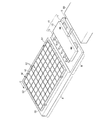
図1は本発明の一実施例による可撓性表示装置の製造装置を示した斜視図であり、図2は図1の可撓性表示装置の製造装置のII−II線による断面図である。
図1に示したように、本発明の一実施例による可撓性表示装置の製造装置は、支持体本体50、支持体本体50を固定するガイド部60、及び外部の真空吸着装置80及び支持体本体50を連結するコネクタ(connector)70を含む。
First, a manufacturing apparatus for a flexible display device according to the present invention will be described in detail.
FIG. 1 is a perspective view illustrating a flexible display device manufacturing apparatus according to an embodiment of the present invention, and FIG. 2 is a cross-sectional view taken along line II-II of the flexible display device manufacturing apparatus of FIG. .
As shown in FIG. 1, a flexible display device manufacturing apparatus according to an embodiment of the present invention includes a
支持体本体50は、可撓性母基板10を固定して、表示装置の後続工程中に発生する可能性のある基板10のベンド(bend)現象、つまり折れ曲がりを防止する。したがって、支持体本体50は、可撓性母基板10を十分に固定することができるように、可撓性母基板10より大きさが大きい。支持体本体50はアルミニウムからなるのが好ましい。
支持体本体50の上部表面には、据置台51が設置される。据置台51は、可撓性母基板10が直接据置かれる部分で、支持体本体50の上部表面で可撓性母基板10の大きさに相応する。
The
On the upper surface of the
据置台51には、複数の溝52が形成されている。溝52全体の平面形状は格子形状であり、断面形状はV字型である。
可撓性母基板10は、ポリエチレンエーテルフタレート(polyethylene ether phthalate)、ポリエチレンナフタレート(polyethylene naphthalate)、ポリカーボネート(polycarbonate)、ポリアリレート(polyarylate)、ポリエーテルイミド(polyether imide)、ポリエーテルスルホン酸(polyether sulfonate)、ポリイミド(polyimide)、またはポリアクリレート(polyacrylate)から選択される少なくとも1つの物質からなる有機膜を含む。プラスチック基板110は、このような有機膜の両面に順次に形成されているアクリル系樹脂などの下部塗布膜(under−coating)(図示せず)、SiO2またはAl2O3などの障壁層(barrier)(図示せず)、及びアクリル系樹脂などの硬性塗布膜(hard−coating)(図示せず)などをさらに含むことができる。このような層及び膜は、プラスチック基板110の物理的、化学的損傷を防止する。
A plurality of
The
支持体本体50の内部には、本体50を貫通する真空路53が形成されている。真空路53は、各溝52と物理的に連通している。真空路53の一側端は、外部と連通するニップル部54を構成する。
ニップル部54は、回動可能に付着されて、選択的に開閉動作する栓55を含む。
ガイド部60は、支持体本体50及びコネクタ70を固定する。より詳細に説明すれば、ガイド部60は、第1領域(A)及び第1領域(A)より高さが低い第2領域(B)からなる。第1領域(A)の上部には支持体本体50が配置され、第2領域(B)の上部にはコネクタ70が配置される。
A
The
The
ガイド部60の第1領域(A)の上部には、複数の固定ピン62が設置されて、支持体本体50が動くのを防止する。
コネクタ70は、ガイド部60の第2領域(B)の上部に固定されている複数の架橋71、架橋71上に位置する本体72、及び本体72から支持体本体50に向かってのびて形成された複数の連結管73を含む。
A plurality of fixing pins 62 are installed on the upper portion of the first region (A) of the
The connector 70 is formed with a plurality of
本体72は、架橋71上をスライド移動するように付着されている。各連結管73の個数はニップル部54の個数と同一で、連結管73の各々は、支持体本体50のニップル部54に相応する形状からなる。したがって、本体72が架橋71上をスライド移動することによって、連結管73がニップル部54に脱着される。
前記で説明したように、ガイド部60は、高さが互いに異なる第1及び第2領域(A、B)からなるので、支持体本体50のニップル部54の位置及びコネクタ70の連結管73の位置を合わせることができる。
The
As described above, since the
一方、コネクタ70の一側には、圧縮器などの真空吸着装置80が連結されている。
それでは、図3乃至図6を参照して、本発明の一実施例による可撓性表示装置の製造装置の動作について詳細に説明する。
図3、図4、図5、及び図6は本発明の一実施例によって可撓性表示装置を製造する工程の一部を順次に示した断面図である。
On the other hand, a
Now, with reference to FIGS. 3 to 6, the operation of the flexible display device manufacturing apparatus according to the embodiment of the present invention will be described in detail.
3, 4, 5, and 6 are cross-sectional views sequentially illustrating a part of a process of manufacturing a flexible display device according to an embodiment of the present invention.
まず、図3に示したように、プラスチックなどの可撓性母基板10の一面に静電発生装置90を利用して静電力を印加する。
その後、図4に示したように、可撓性母基板10をガイド部60上に配置された支持体本体50の据置台51に据置く。この時、可撓性母基板10のうちの静電力が印加された面が支持体本体50の据置台51に接触するようにする。
First, as shown in FIG. 3, an electrostatic force is applied to one surface of a
After that, as shown in FIG. 4, the
その後、真空吸着装置80に連結されたコネクタ70の本体72を支持体本体50の方向に向かってスライド移動させる。そうすると、連結管73及びニップル部54が連結されて、ニップル部54の入口をふさいでいた栓55が上に回動する。したがって、コネクタ70を通じて真空吸着装置80及び真空路53が連通する。
次に、真空吸着装置80を作動させて、真空路53の内部及び真空路53と連結されている溝52を真空状態にして、可撓性母基板10を支持体本体50の据置台に付着させる。
Thereafter, the
Next, the
その後、図5に示したように、コネクタ70の本体72を支持体本体50の反対方向に向かってスライド移動させれば、ニップル部54の栓55は再び下に回動して、ニップル部54の入口がふさがれる。したがって、真空路53及び溝52の内部の真空状態が安定的に維持される。
最後に、図6に示したように、ガイド部60から支持体本体50を分離して、可撓性母基板10上に薄膜パターン15を形成する。この時、可撓性母基板10は、支持体本体50に堅固に固定されているので、曲がったり膨張しない。また、支持体50及び可撓性母基板10の間に接着剤が使用されていないので、接着剤による不良を防止することができる。
Thereafter, as shown in FIG. 5, when the
Finally, as shown in FIG. 6, the
支持体本体50の真空路53及び溝52の内部を一度真空状態にした後には、真空吸着装置80と再び連結する必要がないので、可撓性母基板10上に薄膜パターン15を形成する間に、真空吸着装置80とは独立的に可撓性表示装置の後続工程を進めることができる。また、可撓性母基板10上に静電力を印加した後に、支持体本体50上に真空吸着するので、静電力により互いに引き付け合い、可撓性母基板10及び支持体本体50の間の付着力がより向上する。
Since the inside of the
薄膜パターン15を形成した後には、可撓性母基板10を支持体本体50から分離して、薄膜パターンが形成された他の可撓性基板(図示せず)と結合させて、可撓性表示装置を製造する。例えば、ニップル部54の栓55を回動して、ニップル部54の入口を開いて真空状態を開放することにより可撓性母基板10を支持体本体50から分離する。
一方、可撓性母基板10は、液晶表示装置、有機発光表示装置などの基板として使用されるが、ここでは、液晶表示装置に使用される場合について詳細に説明する。
After the
On the other hand, the
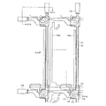
図7は本発明の一実施例による液晶表示装置の配置図であり、図8A及び図8Bは各々図7の液晶表示装置のVIIIa−VIIIa及びVIIIb−VIIIb線による断面図である。
図7乃至図8Bに示したように、本実施例による液晶表示装置は、互いに対向する薄膜トランジスタ表示板100及び共通電極表示板200、及びこれらの間に形成されている液晶層3を含む。
7 is a layout view of a liquid crystal display device according to an embodiment of the present invention, and FIGS. 8A and 8B are cross-sectional views of the liquid crystal display device of FIG. 7 taken along lines VIIIa-VIIIa and VIIIb-VIIIb, respectively.
7 to 8B, the liquid crystal display device according to the present embodiment includes a thin film
まず、薄膜トランジスタ表示板100について説明する。
可撓性基板110上に、複数のゲート線(gate line)121及び複数の維持電極線(storage electrode line)131が形成されている。
ゲート線121は、ゲート信号を伝達し、主に横方向にのびている。各ゲート線121は、上方向に突出した複数のゲート電極(gate electrode)124、及び他の層または外部駆動回路との接続のために面積が広い端部129を含む。ゲート信号を生成するゲート駆動回路(図示せず)は、基板110上に付着される可撓性印刷回路膜(flexible printed circuit film)(図示せず)上に装着されたり、基板110上に直接装着されたり、基板110上に集積される。ゲート駆動回路が基板110上に集積されている場合、ゲート線121がのびて、これと直接連結される。
First, the thin film
A plurality of
The
維持電極線131は、所定の電圧の印加を受けて、ゲート線121とほぼ平行にのびた幹線、及びこれから分かれた複数対の維持電極133a、133bを含む。維持電極線131の各々は、隣接する2つのゲート線121の間に位置し、幹線は2つのゲート線のうちの下側に近く形成されている。維持電極133a、133bの各々は、幹線と連結された固定端、及びその反対側の自由端を含む。維持電極133bの固定端は面積が広く、自由端は直線部分及び曲線部分の二股に分かれている。しかし、維持電極線131の形状及び配置は、多様に変更することができる。
The
ゲート線121及び維持電極線131は、アルミニウム(Al)やアルミニウム合金などのアルミニウム系金属、銀(Ag)や銀合金などの銀系金属、銅(Cu)や銅合金などの銅系金属、モリブデン(Mo)やモリブデン合金などのモリブデン系金属、クロム(Cr)、タンタル(Ta)、及びチタニウム(Ti)などからなることができる。しかし、これらは、物理的性質が異なる2つの導電膜(図示せず)を含む多重膜構造からなることもできる。このうちの1つの導電膜は、信号遅延や電圧降下を減少させることができるように、比抵抗(resistivity)が低い金属、例えば、アルミニウム系金属、銀系金属、銅系金属などからなる。これとは異なって、もう1つの導電膜は、他の物質、特にITO(indium tin oxide)及びIZO(indium zinc oxide)との物理的、化学的、電気的接触特性が優れている物質、例えば、モリブデン系金属、クロム、チタニウム、タンタルなどからなる。これらの組合わせの好ましい例としては、クロムの下部膜及びアルミニウム(合金)の上部膜や、アルミニウム(合金)の下部膜及びモリブデン(合金)の上部膜がある。しかし、ゲート線121及び維持電極線131は、その他にも多様な金属または導電体からなることができる。
The
ゲート線121及び維持電極線131の側面は基板110の面に対して傾いていて、その傾斜角は約30゜乃至約80゜であるのが好ましい。
ゲート線121及び維持電極線131上には、窒化ケイ素(SiNx)または酸化ケイ素(SiOx)などからなるゲート絶縁膜(gate insulating layer)140が形成されている。
The side surfaces of the
A
ゲート絶縁膜140上には、水素化非晶質シリコン(hydrogenated amorphous silicon)(非晶質シリコンは、略してa−Siとする)、多結晶シリコン(polysilicon)、または有機半導体などからなる複数の線状半導体151が形成されている。線状半導体151は、主に縦方向にのびていて、ゲート電極124に向かってのびた複数の突出部(projection)154を含む。線状半導体151は、ゲート線121及び維持電極線131付近で幅が広くなって、これらを幅広く覆っている。
On the
半導体151上には、複数の線状及び島型抵抗性接触部材(ohmic contact)161、165が形成されている。抵抗性接触部材161、165は、リンなどのn型不純物が高濃度にドーピングされているn+水素化非晶質シリコンや、シリサイド(silicide)からなることができる。線状抵抗性接触部材161は、複数の突出部163を含み、突出部163及び島型抵抗性接触部材165は、対をなして半導体151の突出部154に配置されている。
A plurality of linear and island-type
半導体151、154及び抵抗性接触部材161、163、165の側面も基板110の面に対して傾いていて、その傾斜角は約30゜乃至約80゜であるのが好ましい。
抵抗性接触部材161、163、165及びゲート絶縁膜140上には、複数のデータ線(data line)171及び複数のドレイン電極(drain electrode)175が形成されている。
The side surfaces of the
A plurality of
データ線171は、データ信号を伝達し、主に縦方向にのびてゲート線121と交差している。各データ線171は、また、維持電極線131と交差して、隣接する維持電極133a、133bの集合の間を通過する。各データ線171は、ゲート電極124に向かってのびた複数のソース電極(source electrode)173、及び他の層または外部駆動回路との接続のために面積が広い端部179を含む。データ信号を生成するデータ駆動回路(図示せず)は、基板110上に付着される可撓性印刷回路膜(図示せず)上に装着されたり、基板110上に直接装着されたり、基板110上に集積される。データ駆動回路が基板110上に集積されている場合、データ線171がのびて、これと直接連結される。
The
ドレイン電極175は、データ線171と分離されていて、ゲート電極124を中心にソース電極173と対向する。各ドレイン電極175は、面積が広い一側端部177及び棒状の他側端部を有する。面積が広い端部177は維持電極線131の拡張部137と重畳し、棒状の端部はJ字型に曲がったソース電極173で一部が囲まれている。
一つのゲート電極124、一つのソース電極173、及び一つのドレイン電極175は、半導体151の突出部154と共に一つの薄膜トランジスタ(thin film transistor、TFT)を構成し、薄膜トランジスタのチャンネル(channel)は、ソース電極173及びドレイン電極175の間の突出部154に形成される。半導体151が有機半導体である場合、薄膜トランジスタは有機薄膜トランジスタになる。
The
One
データ線171及びドレイン電極175は、モリブデン、クロム、タンタル、及びチタニウムなどの耐火性金属(refractory metal)、またはこれらの合金からなるのが好ましく、耐火性金属膜(図示せず)及び低抵抗導電膜(図示せず)を含む多重膜構造からなることができる。多重膜構造の例としては、クロムまたはモリブデン(合金)の下部膜及びアルミニウム(合金)上部膜の二重膜や、モリブデン(合金)の下部膜、アルミニウム(合金)の中間膜、及びモリブデン(合金)の上部膜の三重膜がある。しかし、データ線171及びドレイン電極175は、その他にも多様な金属または導電体からなることができる。
The
データ線171及びドレイン電極175の側面も基板110の面に対して傾いていて、その傾斜角は約30゜乃至約80゜であるのが好ましい。
抵抗性接触部材161、163、165は、その下の半導体151、154及びその上のデータ線171及びドレイン電極175の間にだけ位置して、これらの間の接触抵抗を減少させる。大部分の箇所では線状半導体151の幅がデータ線171の幅より小さいが、前記で説明したように、ゲート線121と交差する部分で幅が広くなり、表面を平坦にすることによって、データ線171が断線するのを防止する。半導体151、154には、ソース電極173及びドレイン電極175の間をはじめとして、データ線171及びドレイン電極175で覆われずに露出された部分がある。
The side surfaces of the
The
データ線171、ドレイン電極175、及び露出された半導体151、154部分上には、保護膜(passivation layer)180が形成されている。保護膜180は、無機絶縁物または有機絶縁物などからなり、表面が平坦である。無機絶縁物の例としては、窒化ケイ素及び酸化ケイ素がある。有機絶縁物は、感光性(photosensitivity)を有することができ、その誘電定数(dielectric conctant)が約4.0以下であるのが好ましい。しかし、保護膜180は、有機膜の優れた絶縁特性を生かしつつ、露出された半導体151部分に害を及ぼさないように、下部無機膜及び上部有機膜の二重膜構造からなることができる。
A
保護膜180には、データ線171の端部179及びドレイン電極175を各々露出する複数の接触孔(contact hole)182、185が形成されており、保護膜180及びゲート絶縁膜140には、ゲート線121の端部129を露出する複数の接触孔181、維持電極133bの固定端付近の維持電極線131の一部を露出する複数の接触孔183a、そして維持電極133aの自由端の直線部分を露出する複数の接触孔183bが形成されている。
A plurality of
保護膜180上には、複数の画素電極(pixel electrode)191、複数の連結架橋(overpass)83、及び複数の接触補助部材(contact assistant)81、82が形成されている。画素電極191は、接触孔185を通じてドレイン電極175と物理的、電気的に連結されていて、ドレイン電極175からデータ電圧の印加を受ける。データ電圧の印加を受けた画素電極191は、共通電圧(common voltage)の印加を受ける共通電極表示板200の共通電極(common electrode)(図示せず)と共に電場を生成することによって、2つの電極の間の液晶層(図示せず)の液晶分子の配向を決定する。このように決定された液晶分子の配向によって、液晶層を通過する光の偏光が変化する。画素電極191及び共通電極は、キャパシタ(以下、液晶キャパシタ(liquid crystal capacitor)とする)を構成して、薄膜トランジスタがターンオフされた後にも印加された電圧を維持する。
A plurality of
画素電極191は、維持電極133a、133bをはじめとする維持電極線131と重畳する。画素電極191及びこれと電気的に連結されたドレイン電極175が維持電極線131と重畳することによって構成されるキャパシタを「ストレージキャパシタ(storage capacitor)」といい、ストレージキャパシタは、液晶キャパシタの電圧維持能力を強化する。
The
接触補助部材81、82は、各々接触孔181、182を通じてゲート線121の端部129及びデータ線171の端部179と連結される。接触補助部材81、82は、ゲート線121の端部129及びデータ線171の端部179と外部装置との接続を補完して、これらを保護する。
連結架橋83は、ゲート線121を横切って、ゲート線121を間において反対側に位置する接触孔183a、183bを通じて維持電極線131の露出された部分及び維持電極133bの自由端の露出された端部と連結されている。維持電極133a、133bをはじめとする維持電極線131は、連結架橋83と共に、ゲート線121やデータ線171、または薄膜トランジスタの欠陥を修理するのに使用される。
The
The connection bridge 83 crosses the
次に、共通電極表示板200について説明する。
可撓性基板210上に、遮光部材(light blocking member)220が形成されている。遮光部材220は、ブラックマトリックス(black matrix)ともいって、画素電極191と対向する複数の開口領域を定義する一方で、画素電極191の間の光漏れを防止する。
Next, the
A
基板210上には、また、複数のカラーフィルター(color filter)230が形成されていて、遮光部材220で囲まれた開口領域内に大部分が位置するように形成されている。カラーフィルター230は、画素電極190に沿って縦方向に長くのびて、ストライプ(stripe)状に構成することができる。各カラーフィルター230は、赤色、緑色、及び青色の三原色など基本色(primary color)のうちの1つを表示することができる。
A plurality of
カラーフィルター230及び遮光部材220上には、オーバーコート(overcoat)250が形成されている。オーバーコート250は、絶縁物からなって、カラーフィルター230を保護し、カラーフィルター230が露出されるのを防止して、平坦な表面を提供する。
オーバーコート250上には、共通電極270が形成されている。共通電極270は、ITOやIZOなどの透明な導電体からなるのが好ましい。
An
A
表示板100、200の内側面上には、液晶層3を配向するための配向膜(alignment layer)(図示せず)が塗布されていて、表示板100、200の外側面には、1つ以上の偏光子(polarizer)(図示せず)が形成されている。
それでは、図7乃至図8Bに示した液晶表示装置のうちの薄膜トランジスタ表示板100を本発明の一実施例によって製造する方法について、図9乃至図16B及び図7乃至図8Bを参照して詳細に説明する。
An alignment layer (not shown) for aligning the liquid crystal layer 3 is applied on the inner side surfaces of the
7 to 8B, a method of manufacturing the thin film
図9、図11、図13、及び図15は図7乃至図8Bに示した液晶表示装置のうちの薄膜トランジスタ表示板を本発明の一実施例によって製造する方法の中間段階での配置図をその順序によって羅列したものであって、図10A、図10B、図12A、図12B、図14A、図14B、図16A、及び図16Bは図9、図11、図13、及び図15に示した薄膜トランジスタ表示板のXa−Xa、Xb−Xb、XIIa−XIIa、XIIb−XIIb、XIVa−XIVa、XIVb−XIVb、XVIa−XVIa、及びXVIb−XVIb線による断面図である。 9, 11, 13, and 15 are layout diagrams at an intermediate stage of a method of manufacturing a thin film transistor array panel of the liquid crystal display device shown in FIGS. 7 to 8B according to an embodiment of the present invention. FIG. 10A, FIG. 10B, FIG. 12A, FIG. 12B, FIG. 14A, FIG. 14B, FIG. 16A, and FIG. 16B are the thin film transistors shown in FIG. It is sectional drawing by the Xa-Xa, Xb-Xb, XIIa-XIIa, XIIb-XIIb, XIVa-XIVa, XIVb-XIVb, XVIa-XVIa, and XVIb-XVIb line of a display board.
まず、図9乃至図10Bに示したように、前記で説明した図3乃至図6と同様に、支持体本体50の据置台51上に可撓性基板110を付着した後、基板110上の金属膜をスパッタリング(sputtering)などによって順次に積層して写真エッチングして、ゲート電極124及び端部129を含む複数のゲート線121、及び維持電極133a、133bを含む複数の維持電極線131を形成する。
First, as shown in FIGS. 9 to 10B, as in FIGS. 3 to 6 described above, the
図11乃至図12Bに示したように、ゲート絶縁膜140、真性非晶質シリコン層(intrinsic amorphous silicon)150、不純物非晶質シリコン層(extrinsic amorphous silicon)160の3層膜を連続して積層した後、上の2層をパターニングして、複数の線状不純物半導体164及び突出部154を含む複数の線状真性半導体151を形成する。
As shown in FIGS. 11 to 12B, a
次に、図13乃至図14Bに示したように、金属膜をスパッタリングなどによって積層して写真エッチングして、ソース電極173及び端部179を含む複数のデータ線171、複数のドレイン電極175を形成する。
次に、データ線171及びドレイン電極175で覆われずに露出された不純物半導体164部分を除去することによって、突出部163を含む複数の線状抵抗性接触部材161及び複数の島型抵抗性接触部材165を完成する一方で、その下の真性半導体151部分を露出する。露出された真性半導体151部分の表面を安定化するために、後続工程として酸素プラズマを行うのが好ましい。
Next, as shown in FIGS. 13 to 14B, a plurality of
Next, by removing the portion of the
次に、図15乃至図16Bに示したように、化学気相蒸着などによって無機絶縁物を積層したり、感光性有機絶縁物を塗布して、保護膜180を形成する。その後、保護膜180及びゲート絶縁膜140をエッチングして、接触孔181、182、183a、183b、185を形成する。
最後に、図7乃至図8Bに示したように、ITOまたはIZO膜をスパッタリングによって積層して写真エッチングして、複数の画素電極191及び複数の接触補助部材81、82を形成する。その他にも、配向膜(図示せず)を形成する工程を追加することができる。
Next, as shown in FIGS. 15 to 16B, a
Finally, as shown in FIGS. 7 to 8B, ITO or IZO films are stacked by sputtering and photo-etched to form a plurality of
次に、図7乃至図8Bに示した液晶表示装置のうちの共通電極表示板200を本発明の一実施例によって製造する方法について、図17A乃至図17Dを参照して詳細に説明する。
図17Aに示したように、支持体本体50の据置台53上に、真空吸着によって可撓性基板210を付着する。その後、可撓性基板210上に、遮光特性が優れている物質を積層し、マスクを利用して写真エッチングしてパターニングして、遮光部材220を形成する。
Next, a method of manufacturing the
As shown in FIG. 17A, the
次に、図17Bに示したように、可撓性基板210上に感光性組成物を塗布して、互いに異なる3つの色相を表示する複数のカラーフィルター230を形成する。
その後、図17Cに示したように、カラーフィルター230上にオーバーコート250を形成し、図17Dに示したように、オーバーコート250上に共通電極270を積層する。
Next, as shown in FIG. 17B, a photosensitive composition is applied on the
Thereafter, as shown in FIG. 17C, an
その次に、前記のように製造された薄膜トランジスタ表示板100及び共通電極表示板200を結合する。その後、薄膜トランジスタ表示板100及び共通電極表示板200の間に液晶を注入する。この時、薄膜トランジスタ表示板100及び共通電極表示板200の結合前に液晶を滴下させて液晶を注入することもできる。
最後に、製造しようとする表示装置の大きさに応じて薄膜トランジスタ表示板100、共通電極表示板200、及びこれに付着されている支持体本体50を除去する。その後、結合されている薄膜トランジスタ表示板100及び共通電極表示板200を製造しようとする表示装置の大きさに応じて切断して、分離することもできる。
Next, the thin film
Finally, the thin film
図3乃至図6に示した方法で、薄膜パターン15は、有機半導体を含む有機薄膜トランジスタ(organic thin film transistor)を含むこともできる。
また、図3乃至図6に示した方法は、液晶表示装置だけでなく、有機発光表示装置にも適用することができる。
The
Further, the method shown in FIGS. 3 to 6 can be applied not only to the liquid crystal display device but also to the organic light emitting display device.
10 可撓性母基板
15 薄膜パターン
3 液晶層
50 支持体
51 据置台
52 溝
53 真空路
54 ニップル部
55 栓
60 ガイド部
62 固定ピン
70 コネクタ
71 架橋
72 本体
73 連結管
80 真空吸着装置
81、82 接触補助部材
83 連結架橋
90 静電発生装置
100 薄膜トランジスタ表示板
110、210 可撓性基板
121 ゲート線
124 ゲート電極
131 維持電極線
133a、133b 維持電極
140 ゲート絶縁膜
151、154 半導体
161、163、165 抵抗性接触部材
171 データ線
173 ソース電極
175 ドレイン電極
180 保護膜
181、182、183a、183b、185 接触孔
191 画素電極
200 共通電極表示板
220 遮光部材
230 カラーフィルター
250 オーバーコート
270 共通電極
DESCRIPTION OF
Claims (19)
前記支持体本体の表面に位置し、複数の溝が形成されていて、可撓性母基板を据置く据置台、
前記支持体本体を貫通して前記溝と連通していて、一側端が外部と連通している真空路、そして
前記真空路及び外部を連通させるニップル部を含む可撓性表示装置の製造装置。 Support body,
Located on the surface of the support body, a plurality of grooves are formed, and a pedestal for placing a flexible mother board;
An apparatus for manufacturing a flexible display device, comprising: a vacuum path penetrating through the support body and communicating with the groove, and having one end communicating with the outside; and a nipple portion communicating the vacuum path and the exterior .
前記可撓性母基板を支持体に据置く段階、
前記可撓性母基板を真空で吸着して前記支持体に付着する段階、そして
前記可撓性母基板上に薄膜パターンを形成する段階を含む可撓性表示装置の製造方法。 Applying an electrostatic force to one surface of the flexible mother board;
Placing the flexible mother substrate on a support;
A method for manufacturing a flexible display device, comprising: adsorbing the flexible mother substrate in a vacuum and attaching the flexible mother substrate to the support; and forming a thin film pattern on the flexible mother substrate.
外部の真空吸着装置及び前記支持体を貫通する真空路を連結する段階、
前記真空吸着装置を利用して前記真空路を真空状態にする段階、そして
前記真空吸着装置及び前記支持体を分離する段階を含む請求項10に記載の可撓性表示装置の製造方法。 The vacuum adsorption step includes
Connecting an external vacuum suction device and a vacuum path penetrating the support;
The method for manufacturing a flexible display device according to claim 10, comprising: a step of making the vacuum path in a vacuum state using the vacuum suction device; and a step of separating the vacuum suction device and the support.
有機膜、
前記有機膜の両面に形成されている下部塗布膜、
前記下部塗布膜上に形成されている障壁層、そして
前記障壁層上に形成されている硬性塗布膜を含む請求項10に記載の可撓性表示装置の製造方法。 The flexible mother board is
Organic film,
A lower coating film formed on both surfaces of the organic film;
The method of manufacturing a flexible display device according to claim 10, comprising: a barrier layer formed on the lower coating film; and a hard coating film formed on the barrier layer.
The method of manufacturing a flexible display device according to claim 10, wherein the thin film pattern includes an organic thin film transistor.
Applications Claiming Priority (1)
| Application Number | Priority Date | Filing Date | Title |
|---|---|---|---|
| KR1020060087934A KR20080023853A (en) | 2006-09-12 | 2006-09-12 | Apparatus of manufacturing flexible display device and method of manufacturing the same |
Publications (2)
| Publication Number | Publication Date |
|---|---|
| JP2008070874A true JP2008070874A (en) | 2008-03-27 |
| JP2008070874A5 JP2008070874A5 (en) | 2010-10-21 |
Family
ID=38961596
Family Applications (1)
| Application Number | Title | Priority Date | Filing Date |
|---|---|---|---|
| JP2007234959A Pending JP2008070874A (en) | 2006-09-12 | 2007-09-11 | Apparatus and method for making flexible display |
Country Status (5)
| Country | Link |
|---|---|
| US (1) | US20080063787A1 (en) |
| EP (1) | EP1901111A3 (en) |
| JP (1) | JP2008070874A (en) |
| KR (1) | KR20080023853A (en) |
| CN (1) | CN101144928A (en) |
Families Citing this family (8)
| Publication number | Priority date | Publication date | Assignee | Title |
|---|---|---|---|---|
| JP5079448B2 (en) * | 2007-10-24 | 2012-11-21 | 株式会社ジャパンディスプレイウェスト | Liquid crystal device and electronic device including the same |
| CN102651331A (en) * | 2011-06-14 | 2012-08-29 | 京东方科技集团股份有限公司 | Substrate tray and manufacturing method of flexible electronic device |
| US9673014B2 (en) | 2012-07-13 | 2017-06-06 | Samsung Display Co., Ltd. | Method of manufacturing display panel |
| KR101973779B1 (en) * | 2012-11-19 | 2019-04-30 | 삼성디스플레이 주식회사 | Method and device of manufacturing flexible display device |
| KR20150017961A (en) * | 2013-08-08 | 2015-02-23 | 삼성디스플레이 주식회사 | Apparatus and method for determining substrate, and manufacturing method for flexible display using the same |
| CN105336875B (en) * | 2014-07-10 | 2017-10-13 | 上海和辉光电有限公司 | Flexible display device and its release method |
| KR102455039B1 (en) * | 2016-03-18 | 2022-10-17 | 삼성디스플레이 주식회사 | Stretchable display device |
| CN110634406A (en) * | 2019-09-25 | 2019-12-31 | 昆山工研院新型平板显示技术中心有限公司 | Flexible cover plate and preparation method thereof |
Citations (7)
| Publication number | Priority date | Publication date | Assignee | Title |
|---|---|---|---|---|
| JP2003255311A (en) * | 2002-02-28 | 2003-09-10 | Shibaura Mechatronics Corp | Method and device for sticking substrate |
| JP2004072108A (en) * | 2002-08-02 | 2004-03-04 | Suss Microtec Lithography Gmbh | Equipment securing thin and flexible substrate |
| JP2004170975A (en) * | 2002-11-15 | 2004-06-17 | Lg Phillips Lcd Co Ltd | Apparatus for manufacturing liquid crystal display element and manufacturing method utilizing the same |
| JP2005101505A (en) * | 2003-03-13 | 2005-04-14 | Ventec-Ges Fuer Venturekapital & Unternehmensberatung Mbh | Mobile and transportable type electrostatic substrate holder |
| JP2005109358A (en) * | 2003-10-01 | 2005-04-21 | Canon Inc | Substrate sucking device, chuck, holding device, and aligner using them |
| JP2006013488A (en) * | 2004-06-23 | 2006-01-12 | Samsung Sdi Co Ltd | Active drive organic field light-emitting display device provided with organic thin-film transistor, and manufacturing method thereof |
| JP2006091822A (en) * | 2004-09-24 | 2006-04-06 | Samsung Electronics Co Ltd | Manufacturing method for flexible display |
Family Cites Families (10)
| Publication number | Priority date | Publication date | Assignee | Title |
|---|---|---|---|---|
| JPS56128919A (en) * | 1980-03-14 | 1981-10-08 | Matsushita Electric Ind Co Ltd | Manufacture of picture display panel |
| JPH10144776A (en) * | 1996-11-13 | 1998-05-29 | Sumitomo Metal Ind Ltd | Vacuum chuck for holding si wafer |
| JP2000332087A (en) * | 1999-05-25 | 2000-11-30 | Sony Corp | Substrate vacuum chuck apparatus |
| US6446948B1 (en) * | 2000-03-27 | 2002-09-10 | International Business Machines Corporation | Vacuum chuck for reducing distortion of semiconductor and GMR head wafers during processing |
| ATE362843T1 (en) * | 2000-03-28 | 2007-06-15 | Toyo Boseki | TRANSPARENT CONDUCTIVE FILM, TRANSPARENT CONDUCTIVE SHEET AND TOUCH SENSITIVE BOARD |
| JP2001287129A (en) * | 2000-04-05 | 2001-10-16 | Bm:Kk | Vacuum chuck |
| US20050036267A1 (en) * | 2003-05-20 | 2005-02-17 | Savas Stephen Edward | Clamp for holding and efficiently removing heat from workpieces |
| US7297414B2 (en) * | 2003-09-30 | 2007-11-20 | Fujifilm Corporation | Gas barrier film and method for producing the same |
| JP4381206B2 (en) * | 2004-03-31 | 2009-12-09 | 淳二 城戸 | Light emitting transistor |
| US20060046269A1 (en) * | 2004-09-02 | 2006-03-02 | Thompson Allen C | Methods and devices for processing chemical arrays |
-
2006
- 2006-09-12 KR KR1020060087934A patent/KR20080023853A/en not_active Application Discontinuation
-
2007
- 2007-08-10 US US11/891,585 patent/US20080063787A1/en not_active Abandoned
- 2007-08-16 EP EP07016070A patent/EP1901111A3/en not_active Withdrawn
- 2007-08-30 CN CNA200710147835XA patent/CN101144928A/en active Pending
- 2007-09-11 JP JP2007234959A patent/JP2008070874A/en active Pending
Patent Citations (7)
| Publication number | Priority date | Publication date | Assignee | Title |
|---|---|---|---|---|
| JP2003255311A (en) * | 2002-02-28 | 2003-09-10 | Shibaura Mechatronics Corp | Method and device for sticking substrate |
| JP2004072108A (en) * | 2002-08-02 | 2004-03-04 | Suss Microtec Lithography Gmbh | Equipment securing thin and flexible substrate |
| JP2004170975A (en) * | 2002-11-15 | 2004-06-17 | Lg Phillips Lcd Co Ltd | Apparatus for manufacturing liquid crystal display element and manufacturing method utilizing the same |
| JP2005101505A (en) * | 2003-03-13 | 2005-04-14 | Ventec-Ges Fuer Venturekapital & Unternehmensberatung Mbh | Mobile and transportable type electrostatic substrate holder |
| JP2005109358A (en) * | 2003-10-01 | 2005-04-21 | Canon Inc | Substrate sucking device, chuck, holding device, and aligner using them |
| JP2006013488A (en) * | 2004-06-23 | 2006-01-12 | Samsung Sdi Co Ltd | Active drive organic field light-emitting display device provided with organic thin-film transistor, and manufacturing method thereof |
| JP2006091822A (en) * | 2004-09-24 | 2006-04-06 | Samsung Electronics Co Ltd | Manufacturing method for flexible display |
Also Published As
| Publication number | Publication date |
|---|---|
| CN101144928A (en) | 2008-03-19 |
| EP1901111A3 (en) | 2011-07-27 |
| EP1901111A2 (en) | 2008-03-19 |
| KR20080023853A (en) | 2008-03-17 |
| US20080063787A1 (en) | 2008-03-13 |
Similar Documents
| Publication | Publication Date | Title |
|---|---|---|
| JP2006337983A (en) | Method of manufacturing flexible display device | |
| JP2006330739A (en) | Manufacturing method of flexible display device | |
| JP5847061B2 (en) | Array substrate and manufacturing method thereof | |
| US7507616B2 (en) | Method of manufacturing a flexible thin film transistor array panel including plastic substrate | |
| US7358124B2 (en) | Thin film transistor array panel and manufacturing method thereof | |
| US20200212147A1 (en) | Display Device and Method for Manufacturing the Same | |
| US7507594B2 (en) | Contact portion and manufacturing method thereof, thin film transistor array panel and manufacturing method thereof | |
| KR101484022B1 (en) | Array Substrate for Liquid Crystal Display and Method for Fabricating The Same | |
| JP2006091822A (en) | Manufacturing method for flexible display | |
| JP2007046053A (en) | Adhesive tape for flexible display and method for producing flexible display using the same | |
| US20090224257A1 (en) | Thin film transistor panel and manufacturing method of the same | |
| JP2008070874A (en) | Apparatus and method for making flexible display | |
| US20060221291A1 (en) | Display device and manufacturing method thereof with an improved seal between the panels | |
| US20050062046A1 (en) | Thin film array panel and manufacturing method thereof | |
| TW201013279A (en) | Liquid crystal display and method of manufacturing the same | |
| KR20140032773A (en) | Foldable multi display device and manufacturing method of the same | |
| US7572658B2 (en) | Method of manufacturing display panel for flexible display device | |
| US11955491B2 (en) | Array substrate and manufacturing method thereof, motherboard and display device | |
| US7767477B2 (en) | Method of manufacturing a thin film transistor array panel | |
| WO2015098192A1 (en) | Semiconductor device and display device | |
| EP3041054A1 (en) | Thin film transistor and display device including the same | |
| US20130075736A1 (en) | Thin film transistor array panel and manufacturing method thereof | |
| KR20110135551A (en) | Method of fabricating thin film pattern and flat display having the thin film pattern | |
| KR20080068348A (en) | Method of manufacturing display device | |
| KR101399200B1 (en) | Liquid crystal display device and method of manufacturing the same |
Legal Events
| Date | Code | Title | Description |
|---|---|---|---|
| A521 | Written amendment |
Free format text: JAPANESE INTERMEDIATE CODE: A523 Effective date: 20100907 |
|
| A621 | Written request for application examination |
Free format text: JAPANESE INTERMEDIATE CODE: A621 Effective date: 20100907 |
|
| A521 | Written amendment |
Free format text: JAPANESE INTERMEDIATE CODE: A523 Effective date: 20110805 |
|
| A977 | Report on retrieval |
Free format text: JAPANESE INTERMEDIATE CODE: A971007 Effective date: 20120816 |
|
| A131 | Notification of reasons for refusal |
Free format text: JAPANESE INTERMEDIATE CODE: A131 Effective date: 20120828 |
|
| A02 | Decision of refusal |
Free format text: JAPANESE INTERMEDIATE CODE: A02 Effective date: 20130212 |