JP2008034412A - Method for manufacturing structure having pattern - Google Patents
Method for manufacturing structure having pattern Download PDFInfo
- Publication number
- JP2008034412A JP2008034412A JP2006202802A JP2006202802A JP2008034412A JP 2008034412 A JP2008034412 A JP 2008034412A JP 2006202802 A JP2006202802 A JP 2006202802A JP 2006202802 A JP2006202802 A JP 2006202802A JP 2008034412 A JP2008034412 A JP 2008034412A
- Authority
- JP
- Japan
- Prior art keywords
- pattern
- stamper
- forming
- manufacturing
- formation
- Prior art date
- Legal status (The legal status is an assumption and is not a legal conclusion. Google has not performed a legal analysis and makes no representation as to the accuracy of the status listed.)
- Granted
Links
Images
Classifications
-
- B—PERFORMING OPERATIONS; TRANSPORTING
- B29—WORKING OF PLASTICS; WORKING OF SUBSTANCES IN A PLASTIC STATE IN GENERAL
- B29C—SHAPING OR JOINING OF PLASTICS; SHAPING OF MATERIAL IN A PLASTIC STATE, NOT OTHERWISE PROVIDED FOR; AFTER-TREATMENT OF THE SHAPED PRODUCTS, e.g. REPAIRING
- B29C59/00—Surface shaping of articles, e.g. embossing; Apparatus therefor
- B29C59/02—Surface shaping of articles, e.g. embossing; Apparatus therefor by mechanical means, e.g. pressing
- B29C59/022—Surface shaping of articles, e.g. embossing; Apparatus therefor by mechanical means, e.g. pressing characterised by the disposition or the configuration, e.g. dimensions, of the embossments or the shaping tools therefor
- B29C2059/023—Microembossing
-
- Y—GENERAL TAGGING OF NEW TECHNOLOGICAL DEVELOPMENTS; GENERAL TAGGING OF CROSS-SECTIONAL TECHNOLOGIES SPANNING OVER SEVERAL SECTIONS OF THE IPC; TECHNICAL SUBJECTS COVERED BY FORMER USPC CROSS-REFERENCE ART COLLECTIONS [XRACs] AND DIGESTS
- Y10—TECHNICAL SUBJECTS COVERED BY FORMER USPC
- Y10S—TECHNICAL SUBJECTS COVERED BY FORMER USPC CROSS-REFERENCE ART COLLECTIONS [XRACs] AND DIGESTS
- Y10S977/00—Nanotechnology
- Y10S977/84—Manufacture, treatment, or detection of nanostructure
- Y10S977/887—Nanoimprint lithography, i.e. nanostamp
Landscapes
- Engineering & Computer Science (AREA)
- Mechanical Engineering (AREA)
- Shaping Of Tube Ends By Bending Or Straightening (AREA)
- Micromachines (AREA)
- Exposure Of Semiconductors, Excluding Electron Or Ion Beam Exposure (AREA)
Abstract
【課題】簡易な方法によってナノスケールのパターンを有する構造体の製造方法を提供する。
【解決手段】パターンを有する構造体の製造方法であって、
被加工層のパターン形成領域に、表面に凹凸構造を有するスタンパをプレスし、第1のパターンを形成する第1のパターン形成工程と(図1(b))、
前記第1のパターンを形成した際のパターン形成領域とスタンパとの相対的な位置を移動させ、前記スタンパを前記パターン形成領域の少なくとも一部にプレスし、第2のパターンを形成する第2のパターン形成工程と(図1(c))、を有する構成とする。
【選択図】 図1A method for producing a structure having a nanoscale pattern by a simple method is provided.
A method of manufacturing a structure having a pattern, comprising:
A first pattern forming step of forming a first pattern by pressing a stamper having a concavo-convex structure on the surface of the pattern forming region of the layer to be processed (FIG. 1B);
A relative position between the pattern formation region and the stamper when the first pattern is formed is moved, the stamper is pressed onto at least a part of the pattern formation region, and a second pattern is formed. And a pattern forming step (FIG. 1C).
[Selection] Figure 1
Description
本発明は、パターンを有する構造体の製造方法に関し、特に、複数回のインプリントによってナノスケールのパターンを有する構造体を製造する方法に関する。 The present invention relates to a method for manufacturing a structure having a pattern, and more particularly to a method for manufacturing a structure having a nanoscale pattern by imprinting a plurality of times.
物体表面に微細な構造を作製する技術として、フォトリソグラフィー、電子線露光、X線露光、ナノインプリントリソグラフィー等といった手法が、従来より知られている。
これらの手法のうち、例えば、フォトリソグラフィーは特許文献1に、電子線露光は特許文献2に、X線露光は特許文献3に、ナノインプリントリソグラフィーは特許文献4等に開示されている。
As techniques for producing a fine structure on the surface of an object, techniques such as photolithography, electron beam exposure, X-ray exposure, nanoimprint lithography and the like are conventionally known.
Among these techniques, for example, photolithography is disclosed in Patent Document 1, electron beam exposure is disclosed in Patent Document 2, X-ray exposure is disclosed in Patent Document 3, and nanoimprint lithography is disclosed in Patent Document 4.
また、上記以外の方法では、アルミニウム等の陽極酸化法や、分子自己組織構造を利用したボトムアップ手法による微細構造の形成法が知られている。例えば、アルミニウム等の陽極酸化法は特許文献5に、またボトムアップ手法による微細構造の形成法は特許文献6等に開示されている。
ところで、上記した従来例の電子線描画やイオンビーム描画のような直描技術では、微細な構造になる程パターン形成に要する時間が長くなる。
そのため、安価に大量生産をする必要のある場合には、X線露光用や紫外線露光用やプレスモールド用のマスクを直描技術等で精密に作製する。そして、フォトリソグラフィーやナノインプリントリソグラフィーで短時間に一括してパターンを形成するという手法が主流になっている。
しかしながら、これらのいずれの手法においても形成できる構造のサイズには限界がある。現在、最も微細な構造を作製することが出来る電子線露光においても、φ10nmの単一ドットを形成することはできるが、これをピッチ20nm以下に配列することは困難である。
また、上記した従来例のアルミニウム等の陽極酸化法や、分子自己組織構造を利用したボトムアップ手法による微細構造の形成法では、規則的な繰り返し構造を大面積に形成するには適しているが、任意の構造を形成することは困難である。
By the way, in the above-described conventional direct drawing techniques such as electron beam drawing and ion beam drawing, the time required for pattern formation becomes longer as the structure becomes finer.
Therefore, when mass production is required at a low cost, a mask for X-ray exposure, ultraviolet exposure, or press mold is precisely produced by a direct drawing technique or the like. A method of forming a pattern in a short time by photolithography or nanoimprint lithography has become the mainstream.
However, there is a limit to the size of the structure that can be formed by any of these methods. At present, even in electron beam exposure that can produce the finest structure, a single dot of φ10 nm can be formed, but it is difficult to arrange it with a pitch of 20 nm or less.
In addition, the conventional anodic oxidation method of aluminum or the like, and the fine structure forming method by the bottom-up method using the molecular self-organization structure are suitable for forming a regular repeating structure in a large area. It is difficult to form any structure.
本発明は、上記課題に鑑み、簡易な方法によってナノスケールのパターンを有する構造体を製造する方法を提供することを目的とするものである。 In view of the above problems, an object of the present invention is to provide a method for producing a structure having a nanoscale pattern by a simple method.
本発明は、上記課題を解決するため、つぎのように構成したパターンを有する構造体の製造方法を提供するものである。
本発明のパターンを有する構造体の製造方法は、
被加工層のパターン形成領域に、表面に凹凸構造を有するスタンパをプレスし、第1のパターンを形成する第1のパターン形成工程と、
前記第1のパターンを形成した際のパターン形成領域とスタンパとの相対的な位置を移動させ、前記スタンパを前記パターン形成領域の少なくとも一部にプレスし、第2のパターンを形成する第2のパターン形成工程と、
を有することを特徴とする。
また、本発明のパターンを有する構造体の製造方法は、
前記スタンパが、前記表面の凹凸構造が四角格子状に配列された構造を備え、
前記第2のパターンが、前記スタンパにより形成された第1のパターンの四角格子配列のユニットセルを成す四角形の重心点の位置に形成されることを特徴とする。
また、本発明のパターンを有する構造体の製造方法は、前記スタンパが、前記表面の凹凸構造が三角格子状に配列された構造を備え、
前記第2のパターンが、前記スタンパにより形成された第1のパターンの三角格子配列のユニットセルを成す三角形の重心点の位置に形成され、
更に、第3のパターンが、前記第1のパターンの前記三角形における前記第2のパターンが形成されていない重心点の位置に形成されることを特徴とする。
また、本発明のパターンを有する構造体の製造方法は、前記被加工層が、熱可塑性材料で形成されることを特徴とする。
また、本発明のパターンを有する構造体の製造方法は、前記第2のパターン形成工程において、熱可塑性材料によって形成された被加工層に熱転写で前記第2のパターンを形成するに際し、
前記第2のパターンの形成条件を、前記第1のパターン形成工程での第1のパターンの形成条件と異なる形成条件とし、
前記第1のパターン形成工程で形成された第1のパターン形状と等しくなるように、前記第2のパターンを形成することを特徴とする。
また、本発明のパターンを有する構造体の製造方法は、前記第2のパターンの形成条件が、
前記被加工層と前記スタンパとの加熱温度の調整、前記加熱温度とプレス圧力の調整、前記加熱温度と前記プレス圧力とプレス時間の調整、のいずれかの選択によることを特徴とする。
In order to solve the above-described problems, the present invention provides a method for manufacturing a structure having a pattern configured as follows.
The manufacturing method of the structure having the pattern of the present invention is as follows.
A first pattern forming step of forming a first pattern by pressing a stamper having a concavo-convex structure on a surface in a pattern forming region of a layer to be processed;
A relative position between the pattern formation region and the stamper when the first pattern is formed is moved, the stamper is pressed onto at least a part of the pattern formation region, and a second pattern is formed. A pattern forming process;
It is characterized by having.
In addition, the method for producing the structure having the pattern of the present invention includes:
The stamper has a structure in which the concavo-convex structure on the surface is arranged in a square lattice pattern,
The second pattern is formed at a position of a barycentric point of a quadrangle that forms a unit cell of a square lattice array of the first pattern formed by the stamper.
Further, in the method for producing a structure having a pattern according to the present invention, the stamper has a structure in which the uneven structure on the surface is arranged in a triangular lattice shape,
The second pattern is formed at the position of the center of gravity of the triangle forming the unit cell of the triangular lattice arrangement of the first pattern formed by the stamper,
Furthermore, the third pattern is formed at the position of the center of gravity where the second pattern is not formed in the triangle of the first pattern.
Moreover, the manufacturing method of the structure which has a pattern of this invention is characterized by the said to-be-processed layer being formed with a thermoplastic material.
Further, in the method for producing a structure having a pattern according to the present invention, in the second pattern formation step, when the second pattern is formed by thermal transfer on a work layer formed of a thermoplastic material,
The formation conditions of the second pattern are different from the formation conditions of the first pattern in the first pattern formation step,
The second pattern is formed so as to be equal to the first pattern shape formed in the first pattern forming step.
Further, in the method of manufacturing a structure having a pattern according to the present invention, the formation condition of the second pattern is
It is characterized by the selection of any one of adjustment of the heating temperature of the layer to be processed and the stamper, adjustment of the heating temperature and pressing pressure, and adjustment of the heating temperature, pressing pressure and pressing time.
本発明によれば、パターンを有する構造体の製造に際し、簡易な方法によってナノスケールのパターンを有する構造体を製造することが可能となる。 According to the present invention, when a structure having a pattern is manufactured, a structure having a nanoscale pattern can be manufactured by a simple method.
つぎに、本発明の実施の形態について説明する。
本実施の形態では、例えば支持基板上に熱可塑性樹脂からなる被加工層を形成し、被加工層に同一のスタンパで複数回プレスを行うパターンを有する構造体の製造方法を構成することができる。
これによって、スタンパの凹凸構造よりも更に微細なパターンを形成することが可能となる。
この方法においては、まず、上記被加工層内のパターン形成領域に、表面にナノメートルスケールの構造体からなる凹凸構造を有するスタンパをプレスして第1のパターンを形成する。
次に、同じスタンパを用いて、上記第1のパターンを形成した際におけるスタンパとパターン形成領域との相対的な位置を移動させ、上記被加工層内のパターン形成領域の少なくとも一部に、スタンパを再度プレスして第2のパターンを形成する。
これにより、上記第1のパターンと上記第2のパターンとによる、スタンパの凹凸構造よりも更に微細なパターンを形成することができる。
Next, an embodiment of the present invention will be described.
In the present embodiment, for example, a method of manufacturing a structure having a pattern in which a processing layer made of a thermoplastic resin is formed on a supporting substrate and the processing layer is pressed a plurality of times with the same stamper can be configured. .
As a result, it is possible to form a finer pattern than the uneven structure of the stamper.
In this method, first, a first pattern is formed by pressing a stamper having a concavo-convex structure made of a nanometer-scale structure on the surface of a pattern forming region in the layer to be processed.
Next, using the same stamper, the relative positions of the stamper and the pattern formation region when the first pattern is formed are moved, and the stamper is placed on at least a part of the pattern formation region in the layer to be processed. Is pressed again to form a second pattern.
Thereby, a finer pattern than the uneven structure of the stamper can be formed by the first pattern and the second pattern.
以上の方法では被加工層に熱可塑性樹脂を用いたが、被加工層はプレスによりスタンパの凹凸形状が転写されるほどの硬度であれば、熱可塑性材料で無くても良い。
なお、熱可塑性材料を用いた場合には、熱可塑性材料とスタンパを熱して硬度を低下させ、スタンパをプレスし、冷却した後にスタンパを剥離すると、低圧で且つより良い凹凸構造の転写を行うことができる。
また、以上の方法では、第1のパターンと第2のパターンによる2回のパターン形成が行われているが、更に複数回のパターン形成を行っても良い。
また、以上の方法では、複数回のプレスによるパターンは、互いに重なり合わない位置に形成される。
In the above method, the thermoplastic resin is used for the layer to be processed. However, the layer to be processed may not be a thermoplastic material as long as the uneven shape of the stamper is transferred by pressing.
If a thermoplastic material is used, the thermoplastic material and the stamper are heated to lower the hardness, the stamper is pressed, and the stamper is peeled off after being cooled, so that a better concavo-convex structure can be transferred at a low pressure. Can do.
In the above method, the pattern formation is performed twice by the first pattern and the second pattern. However, the pattern formation may be performed a plurality of times.
Moreover, in the above method, the pattern by multiple times of press is formed in the position which does not mutually overlap.
また、第2のパターンを形成する際、スタンパの位置を最適化することにより、第1のパターンと同様の配列であり且つ周期が減少するようなパターンを形成することが可能となる。
例えば、スタンパの凹凸構造が四角格子状に配列した周期Aの凸構造体である場合、第2のパターンをプレスする位置が第1のパターンの四角格子配列のユニットセルを成す四角形の重心点であるよう調整する。
これにより、第1のパターンと第2のパターンにより形成されるパターンは、周期がA’(=A/√2)の四角格子状配列となるパターンを形成することが可能となる(図1参照)。
その際、位置調整は、被加工層内に設けたアライメントマークで行っても良いし、ピエゾステージ上に被加工層を配置することで行っても良い。
また、スタンパの凹凸構造が三角格子状に配列したナノスケールの周期Bの凸構造体である場合、第2のパターンをプレスする位置と更に第3のパターンをプレスする位置とを、つぎのように調整する。
すなわち、第2のパターンをプレスする位置が第1のパターンの三角格子配列のユニットセルを成す三角形の重心点であるよう調整する。更に、第3のパターンをプレスする位置が第1のパターンの三角形において第2のパターンが形成されていない重心点であるよう調整する。
これにより、第1と第2と第3のパターンから形成されるパターンは、周期がB’(=B/√3)の三角格子状配列となるパターンを形成することが可能となる(図3参照)。
Further, by optimizing the position of the stamper when forming the second pattern, it is possible to form a pattern having the same arrangement as the first pattern and having a reduced period.
For example, when the concave / convex structure of the stamper is a convex structure having a period A arranged in a square lattice shape, the position where the second pattern is pressed is the barycentric point of the square forming the unit cell of the square lattice arrangement of the first pattern. Adjust to be.
As a result, the pattern formed by the first pattern and the second pattern can form a pattern having a square lattice arrangement with a period of A ′ (= A / √2) (see FIG. 1). ).
At that time, the position adjustment may be performed using an alignment mark provided in the processing layer, or may be performed by arranging the processing layer on the piezo stage.
Further, when the uneven structure of the stamper is a convex structure having a nanoscale period B arranged in a triangular lattice shape, the position where the second pattern is pressed and the position where the third pattern is further pressed are as follows. Adjust to.
That is, adjustment is performed so that the position where the second pattern is pressed is the center of gravity of the triangle forming the unit cell of the triangular lattice arrangement of the first pattern. Furthermore, the position where the third pattern is pressed is adjusted so as to be the center of gravity where the second pattern is not formed in the triangle of the first pattern.
As a result, the pattern formed from the first, second, and third patterns can form a pattern having a triangular lattice arrangement with a period of B ′ (= B / √3) (FIG. 3). reference).
被加工層が熱可塑性材料であり熱インプリントによる形状転写を行う場合、2回目以降のプレスではそれ以前に形成した凹凸構造が影響を受け、形状が変化することがある。
例えば、第1のプレスと第2のプレスを同じ温度・圧力・保持時間で行うと、第1のプレスによる凹凸構造の深さは、第2のプレス後には浅くなる。
そのため、本実施の形態では、第1と第2のプレスによる凹凸構造の形状を等しくする場合には、第2のプレス条件を第1のプレス条件よりも低温で、或いは低温且つ高圧(プレス圧力)、或いは低温且つ高圧且つ長保持時間(プレス時間)で行う、等の方法を用いることができる。
When the layer to be processed is a thermoplastic material and shape transfer is performed by thermal imprinting, the shape may change in the second and subsequent presses due to the influence of the concavo-convex structure formed before that.
For example, when the first press and the second press are performed at the same temperature, pressure, and holding time, the depth of the concavo-convex structure by the first press becomes shallow after the second press.
Therefore, in the present embodiment, when the concavo-convex structure formed by the first and second presses is made equal, the second press condition is lower than the first press condition, or at a lower temperature and higher pressure (press pressure). ), Or a low temperature, high pressure, and long holding time (pressing time).
以下に、本発明の実施例について説明する。
[実施例1]
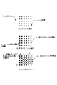
実施例1においては、本発明を適用した正方配列のパターンを有する構造体の製造方法について説明する。
図1に、本実施例におけるパターンを有する構造体の製造方法を説明する図を示す。
本実施例においては、Siからなる支持基板上に、熱可塑性樹脂であるポリメチルメタクリレート(以下、PMMAと記す)を、厚さ200nmになるようスピンコート法で形成し、被加工層とする。
一方、スタンパ1として、ニッケル(Ni)材料の表面に、直径100nm・高さ200nmの円柱状の凸構造2がピッチ300nm(=スタンパの凹凸構造の周期A)の正方格子状に配列した構造のものを、フォトリソグラフィにより作製する(図1(a))。
なお、複数回のパターン形成をする時、パターンが重なり合わないためには、この円柱状凸構造の直径は、周期に対して小さいことが望ましい。
Examples of the present invention will be described below.
[Example 1]
In Example 1, a method for manufacturing a structure having a square array pattern to which the present invention is applied will be described.
FIG. 1 is a diagram illustrating a method for manufacturing a structure having a pattern in this embodiment.
In this embodiment, a polymethyl methacrylate (hereinafter referred to as PMMA), which is a thermoplastic resin, is formed on a support substrate made of Si by a spin coating method so as to have a thickness of 200 nm to form a layer to be processed.
On the other hand, the stamper 1 has a structure in which cylindrical convex structures 2 having a diameter of 100 nm and a height of 200 nm are arranged in a square lattice pattern with a pitch of 300 nm (= period A of the concave-convex structure of the stamper) on the surface of a nickel (Ni) material. A thing is produced by photolithography (FIG. 1A).
In order to prevent the patterns from overlapping when forming the pattern a plurality of times, it is desirable that the diameter of the cylindrical convex structure is small with respect to the period.
次に、スタンパ1の凸構造2を、被加工層と相対向させて保持してピエゾステージ上に固定する。
PMMAとスタンパ1を120℃に加熱し、圧力1tonf/cm2でスタンパを押付けたまま1分間保持し、その後に60℃に冷却してスタンパ1を剥離する。この領域をパターン形成領域とする。
これにより、パターン形成領域には、凸構造2に対応した第1のパターンの凹構造3が形成される(図1(b))。
Next, the convex structure 2 of the stamper 1 is held opposite to the layer to be processed and fixed on the piezo stage.
PMMA and stamper 1 are heated to 120 ° C., held for 1 minute while pressing the stamper at a pressure of 1 tonf / cm 2 , and then cooled to 60 ° C. to peel off stamper 1. This region is defined as a pattern formation region.
Thereby, the concave structure 3 of the 1st pattern corresponding to the convex structure 2 is formed in a pattern formation area (FIG.1 (b)).
次に、同じスタンパ1を用いて、上記第1のパターンを形成した際におけるスタンパとパターン形成領域との相対的な位置を移動させる。そして、スタンパ1の凸構造2が第1のパターンの凹構造3(周期A=300nm)の四角格子配列のユニットセルを成す四角形の重心点であるように、アライメントマークとピエゾステージを使って調整する。
ここで、スタンパ1をプレスすると、第2のパターンの凹構造4が形成され、第1と第2のパターンにより形成されるパターンは、周期がつぎのような四角格子状配列となるパターンを形成することができる。
すなわち、第1のパターンとは配列方向は45度異なり、周期がA’(複数回プレス後に形成される凹凸構造の周期A’)(=A/√2=212nm)の四角格子状配列となるパターンを形成することができる(図1(c))。
Next, using the same stamper 1, the relative positions of the stamper and the pattern formation region when the first pattern is formed are moved. Then, adjustment is performed using alignment marks and a piezo stage so that the convex structure 2 of the stamper 1 is a center of gravity of a quadrangle that forms a unit cell of a square lattice arrangement of the concave structure 3 (period A = 300 nm) of the first pattern. To do.
Here, when the stamper 1 is pressed, the concave structure 4 of the second pattern is formed, and the pattern formed by the first and second patterns forms a pattern in which the period is the following square lattice array. can do.
That is, the arrangement direction is 45 degrees different from that of the first pattern, and a square lattice arrangement having a period of A ′ (period A ′ of the concavo-convex structure formed after pressing a plurality of times) (= A / √2 = 212 nm) is obtained. A pattern can be formed (FIG. 1C).
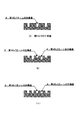
[実施例2]
実施例2においては、実施例1とは異なり、第2のパターンを形成する条件を第1のパターンの形成条件と変える場合の製造方法について説明する。
図2に、本実施例におけるパターンを有する構造体の製造方法を説明する図を示す。
本実施例において、第1のパターンの形成条件は実施例1と同様である。
ここで、第2のパターンを形成する条件を、実施例1のように第1のパターンの形成条件と同じ120℃、1tonf/cm2、1分保持で行うと、つぎのような不都合が生じる場合がある。
すなわち、図2(a)に図示するように、第1のパターンの凹構造3が、再度加熱され且つ周囲から圧力が加わるために、図2(b)のように深さが浅いパターン形状となる。
また、第2のパターンは図2(a)の第1のパターンの凹構造3と同じ形状のものが形成される。そのため、第1のパターンの凹構造3と第2のパターンの凹構造4の形状を等しくするには、第1と第2のパターンの形成条件を変える必要がある。
[Example 2]
In the second embodiment, unlike the first embodiment, a manufacturing method in the case where the conditions for forming the second pattern are changed to the conditions for forming the first pattern will be described.
FIG. 2 is a diagram illustrating a method for manufacturing a structure having a pattern in this example.
In this embodiment, the formation conditions of the first pattern are the same as those in the first embodiment.
Here, if the conditions for forming the second pattern are the same as those for the first pattern as in the first embodiment at 120 ° C., 1 tonf / cm 2 , and held for 1 minute, the following inconvenience occurs. There is a case.
That is, as shown in FIG. 2A, since the concave structure 3 of the first pattern is heated again and pressure is applied from the periphery, a pattern shape having a shallow depth as shown in FIG. Become.
The second pattern is formed in the same shape as the concave structure 3 of the first pattern in FIG. Therefore, in order to make the shapes of the concave structure 3 of the first pattern and the concave structure 4 of the second pattern equal, it is necessary to change the formation conditions of the first and second patterns.
そのため、本実施例では、第1のパターンの形成条件が120℃、1tonf/cm2、1分保持の時、第2のパターンの形成条件を80℃、1tonf/cm2、1分保持とした。
これにより、第1のパターンがやや浅くなるのと同時に、形成される第2のパターンも第1のパターンの初期形状よりは浅くなるため、ほぼ同じ深さにすることが可能となる。この第2のパターンの形成条件の温度を更に下げる場合には、プレス圧力を高くしたり、あるいは保持時間を長くしたりすること、等により調整することが可能である。
Therefore, in this example, when the formation condition of the first pattern is 120 ° C., 1 tonf / cm 2 , and 1 minute hold, the formation condition of the second pattern is 80 ° C., 1 tonf / cm 2 , 1 minute hold. .
As a result, the first pattern becomes slightly shallower, and at the same time, the formed second pattern becomes shallower than the initial shape of the first pattern, so that the first pattern can be made substantially the same depth. When the temperature of the second pattern formation condition is further lowered, it can be adjusted by increasing the press pressure or extending the holding time.
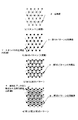
[実施例3]
実施例3においては、三角格子配列のパターンを有する構造体の製造方法について説明する。
図3に、本実施例におけるパターンを有する構造体の製造方法を説明する図を示す。
本実施例において、スタンパ1は、ニッケル(Ni)材料の表面に、直径100nm・高さ200nmの円柱状の凸構造2がピッチ300nm(=スタンパの凹凸構造の周期B)の三角格子状に配列した構造のものが用いられる(図3(a))。
まず、本発明の実施例1と同様に第1のパターンの凹構造3を形成する(図3(b))。
次に、第2のパターンの凹構造4を形成する位置が第1のパターンの三角格子配列のユニットセルを成す三角形の重心点であるよう調整し、パターンを形成する(図3(c))。
更に、第3のパターンをプレスする位置が第1のパターンの三角形において第2のパターンが形成されていない重心点であるよう調整する。
これにより、第1と第2と第3のパターンから形成されるパターンは、周期が173nm(=複数回プレス後に形成される凹凸構造の周期B’=B/√3)の三角格子状配列となるパターンを形成することができる(図3(d))。
[Example 3]
In Example 3, a method of manufacturing a structure having a triangular lattice array pattern will be described.
FIG. 3 is a diagram illustrating a method for manufacturing a structure having a pattern in this example.
In the present embodiment, the stamper 1 has a cylindrical convex structure 2 having a diameter of 100 nm and a height of 200 nm arranged in a triangular lattice shape with a pitch of 300 nm (= period B of the concave-convex structure of the stamper) on the surface of a nickel (Ni) material. The structure having the above structure is used (FIG. 3A).
First, the concave structure 3 having the first pattern is formed as in the first embodiment of the present invention (FIG. 3B).
Next, the position where the concave structure 4 of the second pattern is formed is adjusted so as to be the center of gravity of the triangle forming the unit cell of the triangular lattice arrangement of the first pattern, thereby forming a pattern (FIG. 3C). .
Furthermore, the position where the third pattern is pressed is adjusted so as to be the center of gravity where the second pattern is not formed in the triangle of the first pattern.
Thereby, the pattern formed from the first, second, and third patterns has a triangular lattice-like arrangement with a period of 173 nm (= period B ′ = B / √3 of the concavo-convex structure formed after pressing a plurality of times). Can be formed (FIG. 3D).
なお、本発明に用いられるスタンパは、上記実施例1や実施例3で説明したものに限られるものではない。
例えば、スタンパとして、ニッケル(Ni)材料の表面に、直径50nm・高さ150nmの円柱状の凸構造を備えた構造のもの、あるいはSi材料の表面に、直径50nm・高さ150nmの円柱状の凸構造を備えた構造のもの、等であってもよい。
The stamper used in the present invention is not limited to those described in the first and third embodiments.
For example, the stamper has a structure having a cylindrical convex structure with a diameter of 50 nm and a height of 150 nm on the surface of a nickel (Ni) material, or a cylindrical shape with a diameter of 50 nm and a height of 150 nm on the surface of an Si material. The thing of the structure provided with the convex structure etc. may be sufficient.
1:スタンパ
2:凸構造
3:第1のパターンの凹構造
4:第2のパターンの凹構造
5:スタンパの凹凸構造の周期A
6:複数回プレス後に形成される凹凸構造の周期A’
7:スタンパの凹凸構造の周期B
8:複数回プレス後に形成される凹凸構造の周期B’
9:第3のパターンの凹構造
1: Stamper 2: Convex structure 3: Concave structure of first pattern 4: Concave structure of second pattern 5: Period A of concavo-convex structure of stamper
6: Period A ′ of the concavo-convex structure formed after pressing a plurality of times
7: Period B of the uneven structure of the stamper
8: Period B ′ of the concavo-convex structure formed after pressing a plurality of times
9: Concave structure of third pattern
Claims (6)
被加工層のパターン形成領域に、表面に凹凸構造を有するスタンパをプレスし、第1のパターンを形成する第1のパターン形成工程と、
前記第1のパターンを形成した際のパターン形成領域とスタンパとの相対的な位置を移動させ、前記スタンパを前記パターン形成領域の少なくとも一部にプレスし、第2のパターンを形成する第2のパターン形成工程と、
を有することを特徴とするパターンを有する構造体の製造方法。 A method for producing a structure having a pattern,
A first pattern forming step of forming a first pattern by pressing a stamper having a concavo-convex structure on a surface in a pattern forming region of a layer to be processed;
A relative position between the pattern formation region and the stamper when the first pattern is formed is moved, the stamper is pressed onto at least a part of the pattern formation region, and a second pattern is formed. A pattern forming process;
The manufacturing method of the structure which has a pattern characterized by having.
前記第2のパターンが、前記スタンパにより形成された第1のパターンの四角格子配列のユニットセルを成す四角形の重心点の位置に形成されることを特徴とする請求項1に記載のパターンを有する構造体の製造方法。 The stamper has a structure in which the concavo-convex structure on the surface is arranged in a square lattice pattern,
2. The pattern according to claim 1, wherein the second pattern is formed at a position of a center of gravity of a quadrangle that forms a unit cell of a square lattice array of the first pattern formed by the stamper. Manufacturing method of structure.
前記第2のパターンが、前記スタンパにより形成された第1のパターンの三角格子配列のユニットセルを成す三角形の重心点の位置に形成され、
更に、第3のパターンが、前記第1のパターンの前記三角形における前記第2のパターンが形成されていない重心点の位置に形成されることを特徴とする請求項1に記載のパターンを有する構造体の製造方法。 The stamper has a structure in which the uneven structure on the surface is arranged in a triangular lattice shape,
The second pattern is formed at the position of the center of gravity of the triangle forming the unit cell of the triangular lattice arrangement of the first pattern formed by the stamper,
2. The structure having a pattern according to claim 1, wherein a third pattern is formed at a position of a center of gravity where the second pattern is not formed in the triangle of the first pattern. 3. Body manufacturing method.
前記第2のパターンの形成条件を、前記第1のパターン形成工程での第1のパターンの形成条件と異なる形成条件とし、
前記第1のパターン形成工程で形成された第1のパターン形状と等しくなるように、前記第2のパターンを形成することを特徴とする請求項4に記載のパターンを有する構造体の製造方法。 In the second pattern formation step, when forming the second pattern by thermal transfer on a work layer formed of a thermoplastic material,
The formation conditions of the second pattern are different from the formation conditions of the first pattern in the first pattern formation step,
5. The method for manufacturing a structure having a pattern according to claim 4, wherein the second pattern is formed so as to be equal to the first pattern shape formed in the first pattern forming step.
前記被加工層と前記スタンパとの加熱温度の調整、前記加熱温度とプレス圧力の調整、前記加熱温度と前記プレス圧力とプレス時間の調整、のいずれかの選択によることを特徴とする請求項5に記載のパターンを有する構造体の製造方法。 The formation condition of the second pattern is
6. The method according to claim 5, wherein the heating temperature of the work layer and the stamper is adjusted, the heating temperature and the pressing pressure are adjusted, or the heating temperature, the pressing pressure and the pressing time are adjusted. A method for producing a structure having the pattern described in 1.
Priority Applications (3)
| Application Number | Priority Date | Filing Date | Title |
|---|---|---|---|
| JP2006202802A JP5002207B2 (en) | 2006-07-26 | 2006-07-26 | Method for manufacturing structure having pattern |
| US11/773,739 US7976761B2 (en) | 2006-07-26 | 2007-07-05 | Process of production of patterned structure |
| CN2007101391055A CN101112789B (en) | 2006-07-26 | 2007-07-25 | Process of production of patterned structure |
Applications Claiming Priority (1)
| Application Number | Priority Date | Filing Date | Title |
|---|---|---|---|
| JP2006202802A JP5002207B2 (en) | 2006-07-26 | 2006-07-26 | Method for manufacturing structure having pattern |
Publications (3)
| Publication Number | Publication Date |
|---|---|
| JP2008034412A true JP2008034412A (en) | 2008-02-14 |
| JP2008034412A5 JP2008034412A5 (en) | 2009-09-10 |
| JP5002207B2 JP5002207B2 (en) | 2012-08-15 |
Family
ID=38985377
Family Applications (1)
| Application Number | Title | Priority Date | Filing Date |
|---|---|---|---|
| JP2006202802A Expired - Fee Related JP5002207B2 (en) | 2006-07-26 | 2006-07-26 | Method for manufacturing structure having pattern |
Country Status (3)
| Country | Link |
|---|---|
| US (1) | US7976761B2 (en) |
| JP (1) | JP5002207B2 (en) |
| CN (1) | CN101112789B (en) |
Cited By (5)
| Publication number | Priority date | Publication date | Assignee | Title |
|---|---|---|---|---|
| JP2010507715A (en) * | 2006-10-25 | 2010-03-11 | エージェンシー・フォー・サイエンス・テクノロジー・アンド・リサーチ | Modification of substrate surface wettability |
| JP2010147295A (en) * | 2008-12-19 | 2010-07-01 | Canon Inc | Method for forming three-dimensional microstructure, and method for manufacturing liquid ejecting head |
| JP2010532283A (en) * | 2007-06-27 | 2010-10-07 | エイジェンシー・フォー・サイエンス,テクノロジー・アンド・リサーチ | Method for making a secondary imprint on an imprinted polymer |
| KR101121653B1 (en) * | 2009-02-04 | 2012-03-09 | 에이에스엠엘 네델란즈 비.브이. | imprint lithography method and apparatus |
| CN102566258A (en) * | 2010-12-29 | 2012-07-11 | 中芯国际集成电路制造(上海)有限公司 | Double imprint method |
Families Citing this family (5)
| Publication number | Priority date | Publication date | Assignee | Title |
|---|---|---|---|---|
| JP5294565B2 (en) * | 2006-03-17 | 2013-09-18 | キヤノン株式会社 | Light emitting device and method for manufacturing light emitting device |
| JP2009238777A (en) * | 2008-03-25 | 2009-10-15 | Toshiba Corp | Manufacturing method of semiconductor device |
| US20140147543A1 (en) * | 2011-07-11 | 2014-05-29 | Scivax Corporation | Fluid pressure imprinting device provided with pressurization unit securing tool |
| US10341914B2 (en) * | 2014-02-18 | 2019-07-02 | Qualcomm Incorporated | Antenna selection in LTE/LTE-A networks with unlicensed spectrum |
| CN110299284B (en) | 2018-03-23 | 2020-11-03 | 联华电子股份有限公司 | Patterning method and patterning structure |
Citations (8)
| Publication number | Priority date | Publication date | Assignee | Title |
|---|---|---|---|---|
| JP2002543582A (en) * | 1999-04-21 | 2002-12-17 | ミヌタ・テクノロジー・カンパニー・リミテッド | Fine pattern forming method |
| JP2003519923A (en) * | 1999-12-30 | 2003-06-24 | コーニンクレッカ フィリップス エレクトロニクス エヌ ヴィ | A method for measuring consistency using the lattice structure of latent images |
| US20050005801A1 (en) * | 2003-07-05 | 2005-01-13 | Erich Thallner | Method and device for forming a surface structure on a wafer |
| JP2006005023A (en) * | 2004-06-15 | 2006-01-05 | Dainippon Printing Co Ltd | Imprint method, imprint apparatus and mold member thereof, and patterning method for forming semiconductor elements using the imprint method. |
| JP2006191087A (en) * | 2004-12-30 | 2006-07-20 | Asml Netherlands Bv | Imprint lithography |
| JP2006191089A (en) * | 2004-12-30 | 2006-07-20 | Asml Netherlands Bv | Imprint lithography |
| JP2006295167A (en) * | 2005-04-08 | 2006-10-26 | Asml Netherlands Bv | Lithography apparatus utilizing a plurality of pattern forming devices and device manufacturing method |
| JP2007230229A (en) * | 2006-02-01 | 2007-09-13 | Canon Inc | Imprint mold, method for producing structure using the mold, and method for producing member |
Family Cites Families (16)
| Publication number | Priority date | Publication date | Assignee | Title |
|---|---|---|---|---|
| JPH0521310A (en) | 1991-07-11 | 1993-01-29 | Canon Inc | Formation of fine pattern |
| US20040137734A1 (en) | 1995-11-15 | 2004-07-15 | Princeton University | Compositions and processes for nanoimprinting |
| US6518189B1 (en) | 1995-11-15 | 2003-02-11 | Regents Of The University Of Minnesota | Method and apparatus for high density nanostructures |
| US6482742B1 (en) | 2000-07-18 | 2002-11-19 | Stephen Y. Chou | Fluid pressure imprint lithography |
| US6309580B1 (en) | 1995-11-15 | 2001-10-30 | Regents Of The University Of Minnesota | Release surfaces, particularly for use in nanoimprint lithography |
| US5772905A (en) | 1995-11-15 | 1998-06-30 | Regents Of The University Of Minnesota | Nanoimprint lithography |
| US6602620B1 (en) | 1998-12-28 | 2003-08-05 | Kabushiki Kaisha Toshiba | Magnetic recording apparatus, magnetic recording medium and manufacturing method thereof |
| US7322287B2 (en) | 2000-07-18 | 2008-01-29 | Nanonex Corporation | Apparatus for fluid pressure imprint lithography |
| US7211214B2 (en) | 2000-07-18 | 2007-05-01 | Princeton University | Laser assisted direct imprint lithography |
| JP2003068618A (en) | 2001-08-28 | 2003-03-07 | Canon Inc | Exposure apparatus, device manufacturing method, semiconductor manufacturing factory, and exposure apparatus maintenance method |
| JP3830386B2 (en) | 2001-12-20 | 2006-10-04 | 英夫 吉田 | Anodizing method and processing equipment therefor |
| US6999156B2 (en) | 2002-09-30 | 2006-02-14 | Chou Stephen Y | Tunable subwavelength resonant grating filter |
| WO2004044654A2 (en) | 2002-11-12 | 2004-05-27 | Princeton University | Compositions and processes for nanoimprinting |
| JP2004296780A (en) | 2003-03-27 | 2004-10-21 | Canon Inc | X-ray exposure equipment |
| JP4093574B2 (en) * | 2003-09-22 | 2008-06-04 | 株式会社東芝 | Method for manufacturing imprint stamper and method for manufacturing magnetic recording medium |
| JP2005101201A (en) | 2003-09-24 | 2005-04-14 | Canon Inc | Nanoimprint equipment |
-
2006
- 2006-07-26 JP JP2006202802A patent/JP5002207B2/en not_active Expired - Fee Related
-
2007
- 2007-07-05 US US11/773,739 patent/US7976761B2/en not_active Expired - Fee Related
- 2007-07-25 CN CN2007101391055A patent/CN101112789B/en not_active Expired - Fee Related
Patent Citations (8)
| Publication number | Priority date | Publication date | Assignee | Title |
|---|---|---|---|---|
| JP2002543582A (en) * | 1999-04-21 | 2002-12-17 | ミヌタ・テクノロジー・カンパニー・リミテッド | Fine pattern forming method |
| JP2003519923A (en) * | 1999-12-30 | 2003-06-24 | コーニンクレッカ フィリップス エレクトロニクス エヌ ヴィ | A method for measuring consistency using the lattice structure of latent images |
| US20050005801A1 (en) * | 2003-07-05 | 2005-01-13 | Erich Thallner | Method and device for forming a surface structure on a wafer |
| JP2006005023A (en) * | 2004-06-15 | 2006-01-05 | Dainippon Printing Co Ltd | Imprint method, imprint apparatus and mold member thereof, and patterning method for forming semiconductor elements using the imprint method. |
| JP2006191087A (en) * | 2004-12-30 | 2006-07-20 | Asml Netherlands Bv | Imprint lithography |
| JP2006191089A (en) * | 2004-12-30 | 2006-07-20 | Asml Netherlands Bv | Imprint lithography |
| JP2006295167A (en) * | 2005-04-08 | 2006-10-26 | Asml Netherlands Bv | Lithography apparatus utilizing a plurality of pattern forming devices and device manufacturing method |
| JP2007230229A (en) * | 2006-02-01 | 2007-09-13 | Canon Inc | Imprint mold, method for producing structure using the mold, and method for producing member |
Cited By (8)
| Publication number | Priority date | Publication date | Assignee | Title |
|---|---|---|---|---|
| JP2010507715A (en) * | 2006-10-25 | 2010-03-11 | エージェンシー・フォー・サイエンス・テクノロジー・アンド・リサーチ | Modification of substrate surface wettability |
| JP2010532283A (en) * | 2007-06-27 | 2010-10-07 | エイジェンシー・フォー・サイエンス,テクノロジー・アンド・リサーチ | Method for making a secondary imprint on an imprinted polymer |
| JP2010147295A (en) * | 2008-12-19 | 2010-07-01 | Canon Inc | Method for forming three-dimensional microstructure, and method for manufacturing liquid ejecting head |
| US8366862B2 (en) | 2008-12-19 | 2013-02-05 | Canon Kabushiki Kaisha | Method for forming structure and method for manufacturing liquid ejecting head |
| KR101121653B1 (en) * | 2009-02-04 | 2012-03-09 | 에이에스엠엘 네델란즈 비.브이. | imprint lithography method and apparatus |
| US8696969B2 (en) | 2009-02-04 | 2014-04-15 | Asml Netherlands B.V. | Imprint lithography method and apparatus |
| CN102566258A (en) * | 2010-12-29 | 2012-07-11 | 中芯国际集成电路制造(上海)有限公司 | Double imprint method |
| CN102566258B (en) * | 2010-12-29 | 2013-09-18 | 中芯国际集成电路制造(上海)有限公司 | Double imprint method |
Also Published As
| Publication number | Publication date |
|---|---|
| US7976761B2 (en) | 2011-07-12 |
| CN101112789A (en) | 2008-01-30 |
| US20080023880A1 (en) | 2008-01-31 |
| JP5002207B2 (en) | 2012-08-15 |
| CN101112789B (en) | 2012-04-25 |
Similar Documents
| Publication | Publication Date | Title |
|---|---|---|
| US7976761B2 (en) | Process of production of patterned structure | |
| EP2627605B1 (en) | Process for producing highly ordered nanopillar or nanohole structures on large areas | |
| JP5499668B2 (en) | Imprint mold and pattern forming method using the mold | |
| JP6951226B2 (en) | How to control extrusion during imprint template duplication process | |
| JPWO2005057634A1 (en) | Pattern formation method using nanoimprint and apparatus for executing the method | |
| JP5114962B2 (en) | Imprint mold, imprint evaluation apparatus using the same, resist pattern forming method, and imprint mold manufacturing method | |
| US20100264560A1 (en) | Imprint lithography apparatus and method | |
| JP2006108649A (en) | Nanoimprint mold, method for forming nanopattern, and resin molding | |
| US8163656B2 (en) | Process for adjusting the size and shape of nanostructures | |
| KR100912598B1 (en) | Nano imprint stamp with dummy nano pattern and nano imprinting method using same | |
| JP4646705B2 (en) | Mold manufacturing method and molded product manufacturing method | |
| JP2010171109A (en) | Imprinting mold precursor and method of manufacturing the imprinting mold precursor | |
| KR102096608B1 (en) | A Roll to Roll Imprint Flexible Mold with Enhanced Demolding and Method of Manufacturing Pptical Waveguide Using the Same | |
| JP2008070556A (en) | Optical member manufacturing method and optical member molding die manufacturing method | |
| CN117970745B (en) | A method for reshaping a legacy structure to generate a new nanostructure | |
| KR20210028829A (en) | Micro product with high aspect ratio micro pattern and manufacturing mehtod thereof | |
| JP2007237360A (en) | Manufacturing method of structure having concavo-convex pattern, structure having concavo-convex pattern | |
| KR20210005430A (en) | Manufacturing mehtod of mandrel for manufacturing micro product, manufacturing method of mold for manufacturing micro product and mold for manufacturing micro product | |
| JP2007241035A (en) | Manufacturing method of structure having concavo-convex pattern, structure having concavo-convex pattern | |
| JP2007313814A (en) | Mold and manufacturing method thereof | |
| JP2008006638A (en) | Imprint mold and imprint mold manufacturing method | |
| TW201619043A (en) | Micro/nano-molding template and method of forming micro-structure on substrate by use of such micro/nano-molding template | |
| JP5790798B2 (en) | Imprint mold and pattern forming method using the mold | |
| JP2006015698A (en) | Material sheet of press-molded body and press-molding method using the same | |
| CN108227376A (en) | A kind of preparation method of micro-structure, impression formboard, display base plate |
Legal Events
| Date | Code | Title | Description |
|---|---|---|---|
| A521 | Written amendment |
Free format text: JAPANESE INTERMEDIATE CODE: A523 Effective date: 20090724 |
|
| A621 | Written request for application examination |
Free format text: JAPANESE INTERMEDIATE CODE: A621 Effective date: 20090724 |
|
| A977 | Report on retrieval |
Free format text: JAPANESE INTERMEDIATE CODE: A971007 Effective date: 20110810 |
|
| A131 | Notification of reasons for refusal |
Free format text: JAPANESE INTERMEDIATE CODE: A131 Effective date: 20110812 |
|
| A521 | Written amendment |
Free format text: JAPANESE INTERMEDIATE CODE: A523 Effective date: 20111005 |
|
| TRDD | Decision of grant or rejection written | ||
| A01 | Written decision to grant a patent or to grant a registration (utility model) |
Free format text: JAPANESE INTERMEDIATE CODE: A01 Effective date: 20120515 |
|
| A01 | Written decision to grant a patent or to grant a registration (utility model) |
Free format text: JAPANESE INTERMEDIATE CODE: A01 |
|
| A61 | First payment of annual fees (during grant procedure) |
Free format text: JAPANESE INTERMEDIATE CODE: A61 Effective date: 20120521 |
|
| FPAY | Renewal fee payment (event date is renewal date of database) |
Free format text: PAYMENT UNTIL: 20150525 Year of fee payment: 3 |
|
| RD03 | Notification of appointment of power of attorney |
Free format text: JAPANESE INTERMEDIATE CODE: R3D03 |
|
| LAPS | Cancellation because of no payment of annual fees |