JP5002174B2 - Pattern forming method and mold manufacturing method - Google Patents
Pattern forming method and mold manufacturing method Download PDFInfo
- Publication number
- JP5002174B2 JP5002174B2 JP2006075053A JP2006075053A JP5002174B2 JP 5002174 B2 JP5002174 B2 JP 5002174B2 JP 2006075053 A JP2006075053 A JP 2006075053A JP 2006075053 A JP2006075053 A JP 2006075053A JP 5002174 B2 JP5002174 B2 JP 5002174B2
- Authority
- JP
- Japan
- Prior art keywords
- substrate
- pattern
- forming method
- pattern forming
- stretching
- Prior art date
- Legal status (The legal status is an assumption and is not a legal conclusion. Google has not performed a legal analysis and makes no representation as to the accuracy of the status listed.)
- Expired - Fee Related
Links
Images


Landscapes
- Micromachines (AREA)
- Exposure Of Semiconductors, Excluding Electron Or Ion Beam Exposure (AREA)
Description
本発明はナノインプリントのモールドとして使用可能な微細構造体の製造方法に関するものである。 The present invention relates to a method for producing a microstructure that can be used as a mold for nanoimprinting.
微細構造体の作製方法ナノインプリント法が知られている。しかし、ナノインプリント法は、作製したい構造体に応じた凹凸形状のモールドを作製し、これを用いて基板表面に凹凸を作製するため、モールドとして所望の構造の反転パターンを作成する必要がある。 A nanoimprint method for producing a fine structure is known. However, in the nanoimprint method, a concave-convex mold corresponding to a structure to be manufactured is manufactured, and a concave-convex pattern is formed on the substrate surface using the mold. Therefore, it is necessary to create a reverse pattern having a desired structure as a mold.
一方、伸縮可能な基板を用い、印刷用インキパターンを表面に形成した後に基板を延伸又は収縮し、被印刷基板にパターンを転写するインキパターン形成方法が提案されている(特許文献1)。本手法を用いればリソグラフィー等で形成した構造体をより微細化することが可能である。
しかし、伸縮可能な材料を基板として用い、基板表面にパターン形成後に基板を縮小することによりパターンを縮小するプロセスにおいて、伸縮するため基板を冶具で固定する時に基板が容易に変形する。これにより基板を牽引して延伸する時に、牽引力や延伸量で制御すると、基板固定前からの基板延伸量の検出が困難である。このため延伸後の基板表面にパターン形成した後に基板を収縮すると基板表面に形成されるパターンがゆがみ、所望のパターンを得ることが困難である。 However, in the process of reducing the pattern by using a stretchable material as the substrate and reducing the substrate after forming the pattern on the substrate surface, the substrate is easily deformed when the substrate is fixed with a jig because of the expansion and contraction. Accordingly, when the substrate is pulled and stretched, if it is controlled by the pulling force or the stretch amount, it is difficult to detect the stretch amount of the substrate from before the substrate is fixed. For this reason, when the substrate is shrunk after the pattern is formed on the stretched substrate surface, the pattern formed on the substrate surface is distorted, and it is difficult to obtain a desired pattern.
そこで本発明は、所望のパターンを精度よく形成する方法及びその方法を用いたモールドの製造方法を提供することを目的とする。 Therefore, an object of the present invention is to provide a method for accurately forming a desired pattern and a method for producing a mold using the method.
そこで、本発明は、伸縮可能な基板を用いたパターン形成方法であって、前記基板を延伸させた状態で前記基板の表面にパターンを形成する工程と、前記基板に設けられた変位量検出用マークの検出結果に基づいて、前記パターンが形成された前記基板の延伸量を制御する工程とを有することを特徴とするパターン形成方法を提供するものである。 Accordingly, the present invention provides a pattern forming method using a stretchable substrate, the step of forming a pattern on the surface of the substrate in a state in which the substrate is stretched, and a displacement amount detection provided on the substrate. based on the detection result of the mark, there is provided a pattern forming method characterized by a step of controlling the amount of stretching of the substrate on which the pattern is formed.
本発明によれば、基板の固定時に基板が変形していても、パターン形成後に基板の収縮により得られる縮小パターンのゆがみ量を低減することが可能となる。 According to the present invention, even if the substrate is deformed when the substrate is fixed, the amount of distortion of the reduced pattern obtained by contraction of the substrate after pattern formation can be reduced.
より具体的に以下で本発明を説明する。
まず、パターン形成方法について説明する。伸縮可能な基板としては弾性率1〜20MPaと低くゴム弾性を有する材料が適している。基板の延伸は概ね弾性変形の範囲内で行うことが好ましい。ただしこれに限定されるものではなく、加圧により表面の面積が縮小する材料ならばどのような材料でも良いし、熱収縮フィルムなど加熱により面積が縮小する材料、UV照射により面積が縮小する材料を用いてもいい。
The present invention will be described more specifically below.
First, a pattern forming method will be described. As the stretchable substrate, a material having a low elastic modulus of 1 to 20 MPa and rubber elasticity is suitable. It is preferable to stretch the substrate within the range of elastic deformation. However, the present invention is not limited to this, and any material may be used as long as the surface area is reduced by pressurization, a material that is reduced in area by heating, such as a heat-shrink film, or a material that is reduced in area by UV irradiation. May be used.
伸縮可能な基板は、延伸するための装置もしくは冶具に基板の一部を固定して延伸する。延伸する方向は短軸でも多軸でも良い。伸縮可能な基板に形成する変位量検出用マークとしては、基板表面に形成した凹凸構造もしくは気泡などの基板内部の空洞を用いることができる。また、基板表面もしくは基板内部に形成した遮光材料を変位量検出用マークとして用いることができる。遮光材料としては半透明材料、反射材料を用いることも可能である。また、磁性材料を用いることもできる。 The stretchable substrate is stretched by fixing a part of the substrate to a stretching apparatus or jig. The extending direction may be short axis or multi-axis. As the displacement detection mark formed on the stretchable substrate, a concave-convex structure formed on the substrate surface or a cavity inside the substrate such as a bubble can be used. Further, a light shielding material formed on the substrate surface or inside the substrate can be used as a displacement detection mark. It is also possible to use a translucent material or a reflective material as the light shielding material. A magnetic material can also be used.
変位量検出用マークは、マークに光、イオン、電子、X線を照射して反射又は透過させて観察することでマーク位置を検知することができる。変位量検出用マークとして磁性材料を用いる時には、表面に磁性材料をコートしたプローブを用いてマーク位置を検知することができる。また、変位量検出用マークとして回折格子を用いる時には、延伸・縮小による回折格子のピッチ変化を回折光の強度分布により検出可能である。回折格子は基板の延伸方向毎に形成することで、多軸方向へ延伸を行う時にも変位量検出用マークとして使用することができる。 The displacement detection mark can detect the mark position by irradiating the mark with light, ions, electrons, and X-rays and observing the reflected or transmitted light. When a magnetic material is used as the displacement detection mark, the mark position can be detected using a probe whose surface is coated with a magnetic material. Further, when a diffraction grating is used as the displacement amount detection mark, a change in pitch of the diffraction grating due to stretching / reduction can be detected from the intensity distribution of the diffracted light. By forming the diffraction grating for each extending direction of the substrate, it can be used as a displacement detection mark even when extending in the multiaxial direction.
弾性部材に外力を加えて(引っ張りや圧縮等の外力を加えない状態から)変形させた状態にする。例えば、弾性部材を引っ張って、引き伸ばした状態にする。その時点で、該部材自体に、あるいは該部材上に所定のパターンを形成する。例えば、外部材に直接凹部や溝を形成したり、該部材上に成膜によりパターンを形成する。前記パターンを形成すると同時に、該パターン自体を利用して、あるいは該部材に設けられている位置検出用のマークにより該部材の位置を認識する。その後、加えている外力を解放あるいは、緩めることで、該部材の変形状態から、変形前の状態あるいはそれに近い状態に戻す。 An external force is applied to the elastic member (from a state in which an external force such as tension or compression is not applied) to make it deform. For example, the elastic member is pulled to a stretched state. At that time, a predetermined pattern is formed on the member itself or on the member. For example, a recess or a groove is formed directly on the outer member, or a pattern is formed on the member by film formation. Simultaneously with the formation of the pattern, the position of the member is recognized using the pattern itself or a position detection mark provided on the member. Thereafter, the applied external force is released or loosened to return the deformed state of the member to the state before deformation or a state close thereto.
その際、前記検出用のマークを、あるいはそれを複数用いることで、パターン形成時点から、該部材を変形前の状態に戻すまでに、該マークを利用しながら、変形の戻り具合を制御することができる。例えば、面内方向に歪をかかえた状態で所定のパターンを形成した場合には、その面内方向の歪を保ったまま、即ち等方的に縮小することができる。これは、パターンを等方的に縮小できることを意味する。一旦、大きなパターンを作成した後、等方的に縮小できる技術は重要である。なお、等方的に縮小後、当該パターンを含む該部材を固めることが好ましい。 At that time, by using the detection mark or a plurality of detection marks, the return of deformation can be controlled while using the mark from the time of pattern formation until the member is returned to the state before deformation. Can do. For example, when a predetermined pattern is formed in a state where a strain is applied in the in-plane direction, the strain can be reduced isotropically while maintaining the strain in the in-plane direction. This means that the pattern can be reduced isotropically. Once a large pattern is created, a technique that can be reduced isotropically is important. Note that it is preferable to harden the member including the pattern after isotropic reduction.
[実施例1]
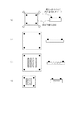
本発明において、基板として0.6mm厚で100mm角のシリコンゴムシートを用いる。図1(a)に示すように、シリコンゴム基板上にスパッタにより銅を100nm厚形成した後に、フォトリソグラフィーおよびエッチングにより、基板四隅に直径5μmの円形銅パターンを形成し変位量検出用マークとする。その後、液状ゴムから成る感光性材料をシリコンゴムシート基板上にスピンコートにより5μm形成し、基板の四隅をクランプし基板を同一面内で延伸する(図1(b))。液状ゴムから成る感光性材料としては、例えば東レダウコーニング社製WL−5351を用いることができる。延伸時には基板四隅に形成した銅パターンを、基板の被加工面の裏面よりカメラで読み込み、マーク重心の相対位置を制御しながら基板を延伸することで、各延伸方向における基板の拡大倍率を所望のものとする。拡大倍率1.5倍にするためには、銅パターン間の相対距離が延伸前と比較してすべて1.5倍になるように基板を延伸する。延伸時に基板を固定後、300nmピッチで幅150nm、高さ100nmのスリットパターン表面に形成した5mm角のニッケルモールドを液状ゴム層に押し当て、モールドを押し当てた面の反対面より液状ゴム層にUV光を照射して液状ゴム層をUV硬化する(図1(c))。硬化後にモールドを離型し、基板を縮小する。これにより基板表面に200nmピッチで幅が100nmの凹凸パターンから成る微細構造体が形成される(図1(d))。凹凸パターン上にニッケルを200nmスパッタした後に、フルファミン酸ニッケルめっき夜により電解ニッケルめっきを50μm厚付与する。ニッケル膜をシリコンゴムより剥離することで、200nmピッチで100nm幅のニッケル微細構造体が得られ、これはモールドとして使用可能である。
[Example 1]
In the present invention, a silicon rubber sheet of 0.6 mm thickness and 100 mm square is used as the substrate. As shown in FIG. 1A, after forming copper to a thickness of 100 nm on a silicon rubber substrate by sputtering, circular copper patterns with a diameter of 5 μm are formed at the four corners of the substrate by photolithography and etching to form displacement detection marks. . Thereafter, a photosensitive material made of liquid rubber is formed on a silicon rubber sheet substrate by spin coating to have a thickness of 5 μm, the four corners of the substrate are clamped, and the substrate is stretched in the same plane (FIG. 1B). As the photosensitive material made of liquid rubber, for example, WL-5351 manufactured by Toray Dow Corning Co., Ltd. can be used. When stretching, the copper pattern formed at the four corners of the substrate is read from the back side of the processed surface of the substrate with a camera, and the substrate is stretched while controlling the relative position of the center of gravity of the mark. Shall. In order to increase the magnification to 1.5 times, the substrate is stretched so that the relative distance between the copper patterns is 1.5 times as much as before stretching. After fixing the substrate during stretching, a 5 mm square nickel mold formed on the surface of a slit pattern having a width of 150 nm and a height of 100 nm at a pitch of 300 nm is pressed against the liquid rubber layer. The liquid rubber layer is UV cured by irradiating with UV light (FIG. 1C). After curing, the mold is released to reduce the substrate. As a result, a microstructure having a concavo-convex pattern having a pitch of 200 nm and a width of 100 nm is formed on the substrate surface (FIG. 1D). After sputtering 200 nm of nickel on the concavo-convex pattern, electrolytic nickel plating is applied to a thickness of 50 μm by night of nickel flufamate plating. By peeling the nickel film from the silicon rubber, a nickel microstructure having a width of 100 nm is obtained at a pitch of 200 nm, which can be used as a mold.
[実施例2]
本発明において、基板として0.6mm厚で100mm角に成形した熱可塑性エラストマーを用いる。熱可塑性エラストマーとしては、例えばスチレン−イソプレンから成る共重合体である日本ゼオン製クインタックを用いることができる。パターン形成には、200nmピッチで三角格子状に配置した100nm径・100nm高の円柱状突起が5mm角のエリアに形成し、その周辺に1辺20mmの正方形の頂点に高さ10μm・直径10μmの突起状パターンを形成したSiモールドを用いる。図2に示すように、Siモールドは100℃に加熱後、拡大倍率が3倍に延伸した熱可塑性エラストマー基板にプレス・離型する。これにより基板表面には、200nmピッチで三角格子状に配置したが100nm径の凹状パターンが5mm角のエリアに形成され、その周囲に1辺20mmの正方形の頂点に、深さ10μm・直径10μmの凹状パターンが形成される。その後、深さ10μm・直径10μmの凹状パターンを変位量検出用マークとして用いる。基板縮小時には変位量検出用マークをカメラで読み取り、凹状パターンの重心位置を検出し1辺が10mm角の正方形になるように基板延伸量を制御する。このとき基板は、拡大倍率が3倍から1.5倍程度に縮小する。これにより、基板表面に100nmピッチで三角格子状に配置した円形凹状パターンから成る微細構造体が得られる。
[Example 2]
In the present invention, a thermoplastic elastomer molded into a 100 mm square with a thickness of 0.6 mm is used as the substrate. As the thermoplastic elastomer, for example, Quintac manufactured by Nippon Zeon, which is a copolymer of styrene-isoprene, can be used. For pattern formation, cylindrical projections with a diameter of 100 nm and a height of 100 nm arranged in a triangular lattice pattern at a pitch of 200 nm are formed in a 5 mm square area, and the apex of a square with a side of 20 mm is 10 μm in height and 10 μm in diameter. A Si mold having a protruding pattern is used. As shown in FIG. 2, after heating the Si mold to 100 ° C., the Si mold is pressed and released from a thermoplastic elastomer substrate stretched by 3 times. As a result, a concave pattern with a diameter of 100 nm is formed in a 5 mm square area on the substrate surface at a pitch of 200 nm but is formed in a square area with a side of 20 mm and a depth of 10 μm and a diameter of 10 μm. A concave pattern is formed. Thereafter, a concave pattern having a depth of 10 μm and a diameter of 10 μm is used as a displacement amount detection mark. When the substrate is reduced, the displacement amount detection mark is read by a camera, the position of the center of gravity of the concave pattern is detected, and the substrate stretching amount is controlled so that one side becomes a 10 mm square. At this time, the magnification of the substrate is reduced from about 3 times to about 1.5 times. Thereby, a fine structure composed of circular concave patterns arranged in a triangular lattice pattern at a pitch of 100 nm on the substrate surface is obtained.
円形凹状パターン上にニッケルを200nmスパッタした後に、フルファミン酸ニッケルめっき夜により電解ニッケルめっきを50μm厚付与する。シリコンゴムを剥離することで、100nmピッチで三角格子状に配置した円柱状パターンから成る微細構造体が得られ、これをモールドとして使用可能である。 After sputtering nickel with a thickness of 200 nm on the circular concave pattern, electrolytic nickel plating is applied to a thickness of 50 μm by night of nickel flufamate plating. By peeling the silicon rubber, a fine structure composed of cylindrical patterns arranged in a triangular lattice pattern at a pitch of 100 nm can be obtained, and this can be used as a mold.
[実施例3]
本発明において、基板として0.6mm厚で100mm角のシリコンゴムシートを用いる。シリコンゴム基板上に20nm厚コバルトをスパッタにより形成した後にフォトリソグラフィーおよびエッチングにより、基板四隅に直径200nmの円柱状のコバルトパターンを形成し変位量検出用マークとする。基板の延伸時に、コバルトから成る変位量検出用マークを、表面をパーマロイでコートした磁気プローブで読み取り、変位量検出用マーク間の相対位置を検知する。そこで実施例1と同様の方法によりシリコンゴムシート上に微細構造体を形成することができる。
[Example 3]
In the present invention, a silicon rubber sheet of 0.6 mm thickness and 100 mm square is used as the substrate. After forming 20 nm thick cobalt on a silicon rubber substrate by sputtering, a cylindrical cobalt pattern having a diameter of 200 nm is formed at the four corners of the substrate by photolithography and etching to form a displacement detection mark. When the substrate is stretched, the displacement detection mark made of cobalt is read with a magnetic probe whose surface is coated with permalloy, and the relative position between the displacement detection marks is detected. Therefore, a fine structure can be formed on the silicon rubber sheet by the same method as in the first embodiment.
[実施例4]
本発明において、基板として0.6mm厚で100mm角のシリコンゴムシートを用いる。シリコンゴムシートは液状シリコンゴムを用いて作製しており、ドライエッチングにより一部に溝を作製したシリコンウェハー上で液状シリコンゴムを熱硬化することにより、図3に示すように、シリコンゴムシートの一部に回折格子を形成する。液状シリコンゴムとしては、例えば東レダウコーニング社製Sylguard 184を用いることができる。シリコンゴム中の回折格子に光を照射しながら基板を延伸することにより、基板の延伸量を計測することが可能である。1μmピッチ溝を形成したシリコンウェハー上で液状シリコンゴムを硬化し、シリコンゴムをシリコンウェハーより離型することで1μmピッチの回折格子が得られる。波長300nm〜750nmの光を基板に対して垂直方向より照射して回折光を検出する時に、入射方向に対して30°の回折光の強度が最大となるピーク波長は、延伸前は350nmであり、回折光が700nmまで延伸することで回折格子を形成したシリコンゴム基板は拡大倍率2倍に延伸していることわかる。延伸時に基板表面に100nmピッチの溝パターンを延伸方向に対して垂直方向にFIBで形成し基板を縮小することで、50nmピッチの溝パターンが得られる。
[Example 4]
In the present invention, a silicon rubber sheet of 0.6 mm thickness and 100 mm square is used as the substrate. The silicon rubber sheet is manufactured using liquid silicon rubber, and the silicon rubber sheet is thermally cured on a silicon wafer in which grooves are partially formed by dry etching, as shown in FIG. A diffraction grating is formed in part. As the liquid silicone rubber, for example, Sylguard 184 manufactured by Toray Dow Corning Co., Ltd. can be used. By stretching the substrate while irradiating the diffraction grating in the silicon rubber with light, it is possible to measure the amount of stretching of the substrate. A liquid silicon rubber is cured on a silicon wafer on which 1 μm pitch grooves are formed, and the silicon rubber is released from the silicon wafer to obtain a 1 μm pitch diffraction grating. When diffracted light is detected by irradiating light with a wavelength of 300 nm to 750 nm from the direction perpendicular to the substrate, the peak wavelength at which the intensity of the diffracted light at 30 ° with respect to the incident direction is maximum is 350 nm before stretching. It can be seen that the silicon rubber substrate on which the diffraction grating is formed by extending the diffracted light to 700 nm is stretched at a magnification of 2 times. A groove pattern with a pitch of 50 nm is obtained by forming a groove pattern with a pitch of 100 nm on the surface of the substrate by FIB in the direction perpendicular to the stretching direction during stretching, and reducing the substrate.
Claims (5)
前記基板を延伸させた状態で前記基板の表面にパターンを形成する工程と、
前記基板に設けられた変位量検出用マークの検出結果に基づいて、前記パターンが形成された前記基板の延伸量を制御する工程とを有することを特徴とするパターン形成方法。 A pattern forming method using a stretchable substrate ,
Forming a pattern on the surface of the substrate in a stretched state of the substrate;
Based on the displacement amount detection mark detection result provided in the substrate, a pattern forming method characterized by a step of controlling the amount of stretching of the substrate on which the pattern is formed.
前記基板の表面に形成したパターンが等方的に縮小されるように前記基板の延伸量を制御することを特徴とする請求項1に記載のパターン形成方法。The pattern forming method according to claim 1, wherein an extension amount of the substrate is controlled so that a pattern formed on the surface of the substrate is isotropically reduced.
前記パターン表面に金属膜を形成する工程と、
該金属膜を前記基板より剥離する工程とを有することを特徴とする金属モールドの製造方法。 Forming a pattern on a substrate by the pattern forming method according to any one of claims 1 to 4,
Forming a metal film on the patterned surface,
Method for producing a metal mold, characterized in Rukoto which have a and Cheng Hao you separated from the substrate and the metal film.
Priority Applications (1)
| Application Number | Priority Date | Filing Date | Title |
|---|---|---|---|
| JP2006075053A JP5002174B2 (en) | 2006-03-17 | 2006-03-17 | Pattern forming method and mold manufacturing method |
Applications Claiming Priority (1)
| Application Number | Priority Date | Filing Date | Title |
|---|---|---|---|
| JP2006075053A JP5002174B2 (en) | 2006-03-17 | 2006-03-17 | Pattern forming method and mold manufacturing method |
Publications (2)
| Publication Number | Publication Date |
|---|---|
| JP2007245318A JP2007245318A (en) | 2007-09-27 |
| JP5002174B2 true JP5002174B2 (en) | 2012-08-15 |
Family
ID=38590132
Family Applications (1)
| Application Number | Title | Priority Date | Filing Date |
|---|---|---|---|
| JP2006075053A Expired - Fee Related JP5002174B2 (en) | 2006-03-17 | 2006-03-17 | Pattern forming method and mold manufacturing method |
Country Status (1)
| Country | Link |
|---|---|
| JP (1) | JP5002174B2 (en) |
Families Citing this family (4)
| Publication number | Priority date | Publication date | Assignee | Title |
|---|---|---|---|---|
| JP2008100419A (en) * | 2006-10-18 | 2008-05-01 | Nippon Telegr & Teleph Corp <Ntt> | Method and apparatus for producing minute structure |
| US7763484B2 (en) * | 2007-06-13 | 2010-07-27 | Sumitomo Electric Industries, Ltd. | Method to form an optical grating and to form a distributed feedback laser diode with the optical grating |
| JP5007976B2 (en) * | 2007-10-17 | 2012-08-22 | 独立行政法人産業技術総合研究所 | Periodic fine relief structure material |
| KR101929925B1 (en) * | 2017-06-16 | 2018-12-18 | 한국기계연구원 | Electrode pattern forming system using a substrate stretching unit and a method for forming an electrode pattern using the same |
Family Cites Families (5)
| Publication number | Priority date | Publication date | Assignee | Title |
|---|---|---|---|---|
| JP4325162B2 (en) * | 2002-08-30 | 2009-09-02 | 凸版印刷株式会社 | Position detection mark and display body on which this detection mark is arranged |
| JP4306212B2 (en) * | 2002-09-27 | 2009-07-29 | 凸版印刷株式会社 | Optical waveguide core manufacturing method |
| JP2005116978A (en) * | 2003-10-10 | 2005-04-28 | Sumitomo Heavy Ind Ltd | Nano imprint equipment and method |
| JP2005276983A (en) * | 2004-03-24 | 2005-10-06 | Matsushita Electric Ind Co Ltd | Electronic component, and manufacturing method and printing method thereof |
| JP2006032423A (en) * | 2004-07-12 | 2006-02-02 | Toshiba Corp | Stamper for imprint processing and manufacturing method thereof |
-
2006
- 2006-03-17 JP JP2006075053A patent/JP5002174B2/en not_active Expired - Fee Related
Also Published As
| Publication number | Publication date |
|---|---|
| JP2007245318A (en) | 2007-09-27 |
Similar Documents
| Publication | Publication Date | Title |
|---|---|---|
| JP5064743B2 (en) | Manufacturing method of structure having recess pattern | |
| JP4401383B2 (en) | Structured device manufacturing | |
| US7704425B2 (en) | Pattern replication with intermediate stamp | |
| JP2008507114A (en) | Composite patterning device for soft lithography | |
| TW200848956A (en) | Devices and methods for pattern generation by ink lithography | |
| JP5002207B2 (en) | Method for manufacturing structure having pattern | |
| TW200932666A (en) | Large area nanopattering method and apparatus | |
| KR101358988B1 (en) | Highly stretchable material beyond intrinsic limits using three-dimensional nanostructures and its fabrication method | |
| JP2007227890A (en) | Imprint lithography | |
| JP2008201029A (en) | Concavo-convex pattern forming sheet and its manufacturing method, and process sheet for manufacturing reflection preventing body, phase difference plate, and optical element | |
| CN107111226B (en) | Method for manufacturing patterned stamp, patterned stamp and imprint method | |
| US10189203B2 (en) | Method for forming micropattern of polyimide using imprinting | |
| JP5761320B2 (en) | Manufacturing method of stamp for micro contact printing | |
| Bhingardive et al. | Soft thermal nanoimprint lithography using a nanocomposite mold | |
| JP5002174B2 (en) | Pattern forming method and mold manufacturing method | |
| JP4757852B2 (en) | Imprint lithography | |
| US8845320B2 (en) | Imprint lithography apparatus | |
| US20060180952A1 (en) | Imprint lithography | |
| KR100956409B1 (en) | Method for manufacturing hybrid nano-imprint mask and method for manufacturing electro-device using the same | |
| JP2007030212A (en) | Manufacturing method of stamper for molding plastic | |
| US20050074697A1 (en) | Method for fabricating masters for imprint lithography and related imprint process | |
| JP4889316B2 (en) | A manufacturing method of a three-dimensional structure, a three-dimensional structure, an optical element, a stencil mask, a manufacturing method of a finely processed product, and a manufacturing method of a fine pattern molded product. | |
| US20120301608A1 (en) | Mould for lithography by nano-imprinting and manufacturing methods | |
| JP5460686B2 (en) | Method for manufacturing structure having pattern | |
| JP5428449B2 (en) | Method for producing master plate for producing stamp for micro contact printing, and master plate for producing stamp for micro contact printing |
Legal Events
| Date | Code | Title | Description |
|---|---|---|---|
| A621 | Written request for application examination |
Free format text: JAPANESE INTERMEDIATE CODE: A621 Effective date: 20090317 |
|
| RD04 | Notification of resignation of power of attorney |
Free format text: JAPANESE INTERMEDIATE CODE: A7424 Effective date: 20100201 |
|
| RD01 | Notification of change of attorney |
Free format text: JAPANESE INTERMEDIATE CODE: A7421 Effective date: 20100630 |
|
| A131 | Notification of reasons for refusal |
Free format text: JAPANESE INTERMEDIATE CODE: A131 Effective date: 20110913 |
|
| A977 | Report on retrieval |
Free format text: JAPANESE INTERMEDIATE CODE: A971007 Effective date: 20110914 |
|
| A521 | Written amendment |
Free format text: JAPANESE INTERMEDIATE CODE: A523 Effective date: 20111114 |
|
| TRDD | Decision of grant or rejection written | ||
| A01 | Written decision to grant a patent or to grant a registration (utility model) |
Free format text: JAPANESE INTERMEDIATE CODE: A01 Effective date: 20120515 |
|
| A01 | Written decision to grant a patent or to grant a registration (utility model) |
Free format text: JAPANESE INTERMEDIATE CODE: A01 |
|
| A61 | First payment of annual fees (during grant procedure) |
Free format text: JAPANESE INTERMEDIATE CODE: A61 Effective date: 20120521 |
|
| FPAY | Renewal fee payment (event date is renewal date of database) |
Free format text: PAYMENT UNTIL: 20150525 Year of fee payment: 3 |
|
| LAPS | Cancellation because of no payment of annual fees |