JP2008016732A - Light-emitting diode driving circuit - Google Patents
Light-emitting diode driving circuit Download PDFInfo
- Publication number
- JP2008016732A JP2008016732A JP2006188443A JP2006188443A JP2008016732A JP 2008016732 A JP2008016732 A JP 2008016732A JP 2006188443 A JP2006188443 A JP 2006188443A JP 2006188443 A JP2006188443 A JP 2006188443A JP 2008016732 A JP2008016732 A JP 2008016732A
- Authority
- JP
- Japan
- Prior art keywords
- current
- emitting diode
- light emitting
- circuit
- current mirror
- Prior art date
- Legal status (The legal status is an assumption and is not a legal conclusion. Google has not performed a legal analysis and makes no representation as to the accuracy of the status listed.)
- Pending
Links
Images


Classifications
-
- H—ELECTRICITY
- H05—ELECTRIC TECHNIQUES NOT OTHERWISE PROVIDED FOR
- H05B—ELECTRIC HEATING; ELECTRIC LIGHT SOURCES NOT OTHERWISE PROVIDED FOR; CIRCUIT ARRANGEMENTS FOR ELECTRIC LIGHT SOURCES, IN GENERAL
- H05B45/00—Circuit arrangements for operating light-emitting diodes [LED]
- H05B45/40—Details of LED load circuits
- H05B45/44—Details of LED load circuits with an active control inside an LED matrix
- H05B45/46—Details of LED load circuits with an active control inside an LED matrix having LEDs disposed in parallel lines
Landscapes
- Led Devices (AREA)
Abstract
Description
本発明は発光ダイオード駆動回路に関し、配列された複数の発光ダイオードそれぞれを駆動する発光ダイオード駆動回路に関する。 The present invention relates to a light emitting diode driving circuit, and more particularly to a light emitting diode driving circuit that drives each of a plurality of light emitting diodes arranged.
プリンタ等において感光体を感光させる手段として、発光ダイオード(以下、「LED」という)をリニアに配列したLEDアレイを用いたものがある。このようなLEDアレイの各LEDを駆動する駆動回路としては、例えば特許文献1,2等に記載されているものがある。 As a means for exposing a photosensitive member in a printer or the like, there is one using an LED array in which light emitting diodes (hereinafter referred to as “LED”) are linearly arranged. As a drive circuit for driving each LED of such an LED array, for example, there are those described in Patent Documents 1 and 2 and the like.
図9は、従来の発光ダイオード駆動回路の一例の回路構成図を示す。この駆動回路は半導体集積回路化されている。 FIG. 9 shows a circuit configuration diagram of an example of a conventional light emitting diode driving circuit. This drive circuit is a semiconductor integrated circuit.
同図中、演算増幅器10の反転入力端子には基準電圧源11より基準電圧Vrefが印加されている。演算増幅器10の出力端子はpチャネルMOS電界効果トランジスタ(以下、単に「MOSトランジスタ」という)M1のゲートに接続されると共に、pチャネルMOSトランジスタM2のゲートに接続されている。MOSトランジスタM1,M2のソースは電源Vdd1に接続されている。MOSトランジスタM1,M2はカレントミラー回路を構成している。
In the figure, a reference voltage Vref is applied from the reference voltage source 11 to the inverting input terminal of the
MOSトランジスタM1のドレインは演算増幅器10の非反転入力端子に接続されると共に、抵抗R1を介して接地されている。MOSトランジスタM2のドレインはnチャネルMOSトランジスタM4のドレインに共通接続されている。
The drain of the MOS transistor M1 is connected to the non-inverting input terminal of the
MOSトランジスタM4のドレインはnチャネルMOSトランジスタM4,M5のゲートに共通接続され、MOSトランジスタM4,M5のソースは接地されており、MOSトランジスタM4,M5はカレントミラー回路を構成している。 The drain of the MOS transistor M4 is commonly connected to the gates of the n-channel MOS transistors M4 and M5, the sources of the MOS transistors M4 and M5 are grounded, and the MOS transistors M4 and M5 constitute a current mirror circuit.
MOSトランジスタM5のドレインはpチャネルMOSトランジスタM6のゲートとドレインに接続されている。MOSトランジスタM6のゲートはアナログスイッチ等のスイッチ15,16それぞれを介してpチャネルMOSトランジスタM7,M8のゲートに接続されている。MOSトランジスタM6,M7,M8のソースは電源Vdd2に接続され、MOSトランジスタM7,M8のドレインはLED(発光ダイオード)18のアノードに接続され、LED18のカソードは接地されている。
The drain of the MOS transistor M5 is connected to the gate and drain of the p-channel MOS transistor M6. The gate of the MOS transistor M6 is connected to the gates of the p-channel MOS transistors M7 and M8 via
スイッチ15,16は、端子17a,17bそれぞれから供給される階調制御用のスイッチ制御信号に応じてオン/オフを切り換える。MOSトランジスタM7,M8はスイッチ15,16がオンのときにMOSトランジスタM6とカレントミラー回路を構成する。スイッチ15はLED18を発光させるタイミングでオンとなり、スイッチ16はLED18の発光輝度を増大させて階調表現を行う場合にオンとなる。
従来の発光ダイオード駆動回路では、カレントミラー回路を構成しているMOSトランジスタM1のドレインであるA点の電位と、MOSトランジスタM2のドレインであるB点の電位が同電位ではないために両トランジスタのドレイン・ソース間電圧が異なり、また、両トランジスタの導通電圧Vtのばらつきは10%程度となるため、MOSトランジスタM1のドレイン電流とMOSトランジスタM2のドレイン電流が両トランジスタのゲート面積の比にならず、カレントミラーの精度が悪いという問題があった。 In the conventional LED driving circuit, since the potential at the point A which is the drain of the MOS transistor M1 constituting the current mirror circuit and the potential at the point B which is the drain of the MOS transistor M2 are not the same potential, Since the drain-source voltage is different and the conduction voltage Vt of both transistors varies about 10%, the drain current of the MOS transistor M1 and the drain current of the MOS transistor M2 do not become the ratio of the gate area of both transistors. There was a problem that the accuracy of the current mirror was poor.
また、MOSトランジスタM4とM5やMOSトランジスタM6とM7,M8が構成する他のカレントミラー回路についても同様にカレントミラーの精度が悪いという問題があった。このため、基準電流Irefが一定であってもLED18に流れる電流が変動し、LED18の発光輝度が変動するという問題があった。 The other current mirror circuits formed by the MOS transistors M4 and M5 and the MOS transistors M6, M7, and M8 also have a problem that the accuracy of the current mirror is similarly poor. For this reason, even if the reference current Iref is constant, there is a problem that the current flowing through the LED 18 varies and the light emission luminance of the LED 18 varies.
本発明は、上記の点に鑑みなされたものであり、発光ダイオードの発光輝度の変動を抑えることができる発光ダイオード駆動回路を提供することを目的とする。 The present invention has been made in view of the above points, and an object of the present invention is to provide a light emitting diode driving circuit capable of suppressing fluctuations in light emission luminance of a light emitting diode.
本発明の発光ダイオード駆動回路は、基準電流を生成する基準電流部と、複数系統のスイッチをオン/オフ制御して前記基準電流に比例した複数系統の駆動電流を生成し発光ダイオードに供給する複数チャネル分の電流出力部からなる発光ダイオード駆動回路であって、
前記基準電流部は、前記基準電流が抵抗を流れることで発生する電圧が一定の基準電圧と同一となるよう前記基準電流を制御する演算増幅器と、
前記基準電流に基づく第1の電流を生成する第1のカレントミラー回路を有し、
各チャネルの前記電流出力部は、前記基準電流部の一部と共に構成され、前記第1の電流に基づく第2の電流を生成する第2のカレントミラー回路と、
前記第2の電流を供給され、前記複数系統のスイッチのうちオンとなったスイッチに対応して前記第2の電流に比例する電流を生成する第3のカレントミラー回路を有し、
前記第1、第2、第3のカレントミラー回路それぞれは、カスケード接続された2段のカレントミラー回路であることにより、発光ダイオードの発光輝度の変動を抑えることができる。
The light emitting diode driving circuit according to the present invention includes a reference current unit that generates a reference current, and a plurality of switches that generate on / off control of a plurality of switches to generate a plurality of driving currents that are proportional to the reference current and that supply the plurality of driving currents to the light emitting diodes. A light-emitting diode driving circuit comprising a current output unit for a channel,
The reference current unit includes an operational amplifier that controls the reference current so that a voltage generated when the reference current flows through a resistor is the same as a constant reference voltage;
A first current mirror circuit that generates a first current based on the reference current;
The current output unit of each channel is configured together with a part of the reference current unit, and a second current mirror circuit that generates a second current based on the first current;
A third current mirror circuit that is supplied with the second current and generates a current proportional to the second current corresponding to a switch that is turned on among the plurality of systems of switches;
Each of the first, second, and third current mirror circuits is a cascaded two-stage current mirror circuit, so that variation in light emission luminance of the light emitting diode can be suppressed.
前記発光ダイオード駆動回路において、
前記第1及び第3のカレントミラー回路を構成し高電圧側の電源に接続される各トランジスタと前記高電圧側の電源との間に抵抗を設けることができる。
In the light emitting diode drive circuit,
A resistor may be provided between each of the transistors constituting the first and third current mirror circuits connected to the high voltage power source and the high voltage power source.
前記発光ダイオード駆動回路において、
前記第2のカレントミラー回路を構成し低電圧側の電源に接続される各トランジスタと前記低電圧側の電源との間に抵抗を設けることができる。
In the light emitting diode drive circuit,
A resistor can be provided between each of the transistors constituting the second current mirror circuit and connected to the low-voltage power supply and the low-voltage power supply.
また、前記発光ダイオード駆動回路において、
前記複数チャネル分の電流出力部を一方向に並べて配置し、前記複数チャネル分の電流出力部の上に電源配線を前記一方向に延在させて配置し、
前記電源配線と各チャネルの前記電流出力部を接続する各チャネルのコンタクト領域の一部を開けて囲むよう前記電源配線を切り欠いたスリットを各チャネルに設けることができる。
In the light emitting diode driving circuit,
The current output portions for the plurality of channels are arranged in one direction, and the power supply wiring is arranged to extend in the one direction on the current output portions for the plurality of channels,
Each channel may be provided with a slit formed by cutting out the power supply wiring so as to open and surround a part of the contact region of each channel connecting the power supply wiring and the current output portion of each channel.
本発明によれば、発光ダイオードの発光輝度の変動を抑えることができる。 According to the present invention, fluctuations in the light emission luminance of the light emitting diode can be suppressed.
以下、図面に基づいて本発明の実施形態について説明する。 Hereinafter, embodiments of the present invention will be described with reference to the drawings.
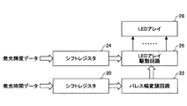
<LEDアレイ駆動回路の構成>
図1は、本発明の発光ダイオード駆動回路を用いたLEDアレイ装置の一実施形態のブロック構成図を示す。このLEDアレイ装置は例えば48チャネル構成である。
<Configuration of LED array driving circuit>
FIG. 1 shows a block diagram of an embodiment of an LED array device using a light emitting diode driving circuit of the present invention. This LED array device has, for example, a 48 channel configuration.
同図中、シフトレジスタ20には1チャネルについて例えば6ビットの発光時間データが48チャネル分時系列で供給され、シフトレジスタ20で順次シフトされてラッチされたのち、パルス幅変調回路22に供給される。パルス幅変調回路22は、チャネル毎に発光時間データで指示されるパルス幅の発光パルスを生成し、48チャネル分の発光パルスをLEDアレイ駆動回路26に供給する。
In the figure, for example, 6-bit light emission time data for one channel is supplied to the
シフトレジスタ24には1チャネルについて例えば6ビットの発光輝度データが48チャネル分時系列で供給され、シフトレジスタ24で順次シフトされてラッチされたのち、LEDアレイ駆動回路26に供給される。LEDアレイ駆動回路26は、チャネル毎に発光輝度データをデコードしてn系統のスイッチ制御信号を生成し、チャネル毎に発光パルスでオンさせるMOSトランジスタを上記n系統のスイッチ制御信号によって決定する。LEDアレイ駆動回路26はLEDアレイ28を構成する48チャネルのLEDをチャネル単位に駆動する。
For example, 6-bit light emission luminance data for 48 channels is supplied to the
<発光ダイオード駆動回路の構成>
図2は、本発明の発光ダイオード駆動回路の一実施形態の回路構成図を示す。この駆動回路は半導体集積回路化されている。
<Configuration of LED driving circuit>
FIG. 2 shows a circuit configuration diagram of an embodiment of a light emitting diode driving circuit of the present invention. This drive circuit is a semiconductor integrated circuit.
同図中、演算増幅器30の反転入力端子には基準電圧源回路31より基準電圧Vrefが印加されている。演算増幅器30の出力端子はpチャネルMOSトランジスタM11,M12それぞれのゲートに接続されている。MOSトランジスタM11,M12それぞれのソースは抵抗R11,R12それぞれを介して電源Vdd1に接続されてカレントミラー回路を構成している。MOSトランジスタM11,M12それぞれのドレインはpチャネルMOSトランジスタM13,M14それぞれのソースに接続されている。
In the figure, the reference voltage Vref is applied from the reference
MOSトランジスタM13,M14のゲートはMOSトランジスタM13のドレインに共通接続されてカレントミラー回路を構成しており、MOSトランジスタM13のドレインは演算増幅器30の非反転入力端子に接続されると共に、抵抗R13の一端に接続されている。抵抗R13の他端は接地されている。
The gates of the MOS transistors M13 and M14 are commonly connected to the drain of the MOS transistor M13 to form a current mirror circuit. The drain of the MOS transistor M13 is connected to the non-inverting input terminal of the
ここで、MOSトランジスタM11,M12にカスケード接続されたMOSトランジスタM13,M14は能動領域で動作してゲート・ソース間電圧Vgsは略同一となるため、カレントミラー回路を構成しているMOSトランジスタM11のドレインであるA点の電位と、MOSトランジスタM12のドレインであるB点の電位は略同電位となる。このために、MOSトランジスタM11,M12のドレイン・ソース間電圧Vdsは略同一となる。 Here, since the MOS transistors M13 and M14 cascade-connected to the MOS transistors M11 and M12 operate in the active region and the gate-source voltage Vgs becomes substantially the same, the MOS transistor M11 constituting the current mirror circuit The potential at the point A that is the drain and the potential at the point B that is the drain of the MOS transistor M12 are substantially the same. For this reason, the drain-source voltage Vds of the MOS transistors M11 and M12 is substantially the same.
また、MOSトランジスタM11,M12のソースに接続された抵抗R11,R12の抵抗値は、MOSトランジスタM11,M12の導通抵抗に比して例えば100倍程度に選定されている。このため、MOSトランジスタM11,M12の導通電圧Vtのばらつきは、抵抗R11,R12がないときに対して1%未満に圧縮され、導通電圧Vtのばらつきは無視できる。 The resistance values of the resistors R11 and R12 connected to the sources of the MOS transistors M11 and M12 are selected to be, for example, about 100 times the conduction resistance of the MOS transistors M11 and M12. For this reason, the variation in the conduction voltage Vt of the MOS transistors M11 and M12 is compressed to less than 1% with respect to the absence of the resistors R11 and R12, and the variation in the conduction voltage Vt can be ignored.
ここで、MOSトランジスタM11,M12のドレイン電流Idは(1)式で表される。なお、λ,μは比例定数、Wはゲート幅、Lはゲート長である。 Here, the drain current Id of the MOS transistors M11 and M12 is expressed by equation (1). Λ and μ are proportional constants, W is a gate width, and L is a gate length.
Id=(1+λ・Vds)×(1/2)×μ×(W/L)×(Vgs−Vt)2 …(1)
(1)式において、MOSトランジスタM11,M12のVdsは略同一であり、Vtのばらつきは無視できるために、MOSトランジスタM11,M12のドレイン電流は両トランジスタのゲート面積の比となり、カレントミラーの精度が向上する。
Id = (1 + λ · Vds) × (1/2) × μ × (W / L) × (Vgs−Vt) 2 (1)
In the equation (1), since the Vds of the MOS transistors M11 and M12 are substantially the same and the variation in Vt can be ignored, the drain current of the MOS transistors M11 and M12 is the ratio of the gate areas of both transistors, and the accuracy of the current mirror Will improve.
MOSトランジスタM14のドレインはnチャネルMOSトランジスタM15のドレインに接続されている。MOSトランジスタM15のゲートはnチャネルMOSトランジスタM16のゲートと接続されてカレントミラー回路を構成している。 The drain of the MOS transistor M14 is connected to the drain of the n-channel MOS transistor M15. The gate of the MOS transistor M15 is connected to the gate of the n-channel MOS transistor M16 to form a current mirror circuit.
MOSトランジスタM15,M16それぞれのソースはnチャネルMOSトランジスタM17,M18それぞれのドレインに接続されている。MOSトランジスタM17,M18のゲートはMOSトランジスタM15のドレインに共通接続されてカレントミラー回路を構成し、MOSトランジスタM17,M18のソースは接地されている。 The sources of the MOS transistors M15 and M16 are connected to the drains of the n-channel MOS transistors M17 and M18. The gates of the MOS transistors M17 and M18 are commonly connected to the drain of the MOS transistor M15 to form a current mirror circuit, and the sources of the MOS transistors M17 and M18 are grounded.
MOSトランジスタM15〜M18はカレントミラー回路がカスケード接続された構成となることにより、MOSトランジスタM11〜M14と同様にして、MOSトランジスタM15,M16のソース電位が略同一となり、ゲート面積が同一の場合MOSトランジスタM15,M16のドレイン電流は略同一となる。なお、MOSトランジスタM15,M16のゲートには電圧源33より定電圧Vaが印加されることでMOSトランジスタM17,M18のドレイン電位はVa−Vgs1(Vgs1はnチャネルMOSトランジスタのゲート・ドレイン間電圧)となる。
Since the MOS transistors M15 to M18 have a configuration in which current mirror circuits are cascade-connected, in the same way as the MOS transistors M11 to M14, the MOS transistors M15 and M16 have substantially the same source potential and the same gate area. The drain currents of the transistors M15 and M16 are substantially the same. Note that a constant voltage Va is applied from the
上記の演算増幅器30,基準電圧源回路31,MOSトランジスタM11〜M15及びM17は基準電流部32を構成しており、MOSトランジスタM13のドレインに基準電流Irefを流す。また、カレントミラー回路によってMOSトランジスタM16のドレインに基準電流Irefに比例した電流が流れる。
The
MOSトランジスタM16のドレインはpチャネルMOSトランジスタM22のドレインに接続されている。MOSトランジスタM22のソースはpチャネルMOSトランジスタM21のドレインに接続されている。MOSトランジスタM21のソースは抵抗R15を介して電源Vdd2に接続されている。 The drain of the MOS transistor M16 is connected to the drain of the p-channel MOS transistor M22. The source of the MOS transistor M22 is connected to the drain of the p-channel MOS transistor M21. The source of the MOS transistor M21 is connected to the power supply Vdd2 via the resistor R15.
MOSトランジスタM21のゲートはMOSトランジスタM22のドレインに接続されると共に、アナログスイッチ等のスイッチ36,38,40それぞれを介してpチャネルMOSトランジスタM23,M25,M27のゲートに接続されている。スイッチ36,38,40がオンするとMOSトランジスタM23,M25,M27のゲート電位をMOSトランジスタM21のゲート電圧と同一にしてMOSトランジスタM23,M25,M27をオンし、スイッチ36,38,40がオフするとMOSトランジスタM23,M25,M27のゲート電位を電源電圧Vdd2としてMOSトランジスタM23,M25,M27をオフする。
The gate of the MOS transistor M21 is connected to the drain of the MOS transistor M22, and is connected to the gates of the p-channel MOS transistors M23, M25, and M27 via
MOSトランジスタM23,M25,M27それぞれのソースは抵抗R16,R17,R18それぞれを介して電源Vdd2に接続されており、MOSトランジスタM23,M25,M27はスイッチ36,38,40がオンのときにMOSトランジスタM21とカレントミラー回路を構成する。
The sources of the MOS transistors M23, M25, M27 are connected to the power supply Vdd2 via the resistors R16, R17, R18, respectively. The MOS transistors M23, M25, M27 are MOS transistors when the
MOSトランジスタM22のゲートはpチャネルMOSトランジスタM24,M26,M28のゲートに接続されている。MOSトランジスタM23,M25,M27それぞれのドレインはMOSトランジスタM24,M26,M28のソースに接続されており、MOSトランジスタM22,M24,M26,M28はカレントミラー回路を構成している。 The gate of the MOS transistor M22 is connected to the gates of the p-channel MOS transistors M24, M26 and M28. The drains of the MOS transistors M23, M25 and M27 are connected to the sources of the MOS transistors M24, M26 and M28, and the MOS transistors M22, M24, M26 and M28 constitute a current mirror circuit.
MOSトランジスタM21〜M28はカレントミラー回路がカスケード接続された構成となることにより、MOSトランジスタM11〜M14と同様にして、MOSトランジスタM21,M23,M25,M27のドレイン電位が略同一となり、ゲート面積が同一の場合MOSトランジスタM22,M24,M26,M28のドレイン電流は略同一となる。ここでは、階調表現を行うために、例えばMOSトランジスタM21,M22のゲート面積に対して、MOSトランジスタM23,M24のゲート面積は6倍、MOSトランジスタM25,M26のゲート面積は3倍、MOSトランジスタM27,M28のゲート面積は2倍というように、ゲート面積をそれぞれ異ならせている。 Since the MOS transistors M21 to M28 are configured by cascading current mirror circuits, the MOS transistors M21, M23, M25, and M27 have substantially the same drain potential and the gate area is the same as the MOS transistors M11 to M14. In the same case, the drain currents of the MOS transistors M22, M24, M26, and M28 are substantially the same. Here, in order to perform gradation expression, for example, the gate areas of the MOS transistors M23 and M24 are six times the gate area of the MOS transistors M21 and M22, the gate areas of the MOS transistors M25 and M26 are three times, and the MOS transistor The gate areas of M27 and M28 are different such that the gate areas are doubled.
なお、MOSトランジスタM22,M24,M26,M28のゲートには電圧源35より定電圧Vbが印加されて、MOSトランジスタM22,M24,M26,M28のソース電位はVb+Vgs2(Vgs2はpチャネルMOSトランジスタのゲート・ドレイン間電圧)とされている。
A constant voltage Vb is applied from the
スイッチ36,38,40それぞれは端子37,39,41それぞれから供給されるn(ここではn=3)系統のスイッチ制御信号に応じてオン/オフを切り換える。なお、nは3に限らない。MOSトランジスタM24,M26,M28のドレインはLED451のアノードに接続され、LED451のカソードは接地されている。
Each of the
ここで、スイッチ36,38,40がオフのときMOSトランジスタM23,M25,M27はオフしLED451に電流は流れない。スイッチ36がオンするとMOSトランジスタM23のドレイン電流がLED451に流れ、スイッチ36,38がオンするとMOSトランジスタM23,M25のドレイン電流の和がLED451に流れ、スイッチ36,38,40がオンするとMOSトランジスタM23,M25,M27のドレイン電流の和がLED451に流れ、LED451は流れる電流が大きくなるほど発光輝度が大となる。
Here, MOS when the
上記のスイッチ36,38,40,MOSトランジスタM16,M18〜M28が1チャネル分の電流出力部441を構成している。LED451はLEDアレイ28の一部である。
m(=48)チャネル分の電流出力部441〜44mそれぞれは同一構成であり、mチャネル分のLED451〜45mそれぞれを駆動する。
Each of the
このように、各カレントミラー回路のカレントミラーの精度を向上できるため、各チャネルのLED451〜45mの発光輝度の変動を抑えることができる。
Thus, since the accuracy of the current mirror of each current mirror circuit can be improved, fluctuations in the emission luminance of the
<発光ダイオード駆動回路の変形例>
図3は、本発明の発光ダイオード駆動回路の一実施形態の変形例の回路構成図を示す。同図中、図2と異なる部分について説明する。図3では、MOSトランジスタM17,M18のソースは抵抗Ra,Rbを介して接地されている。なお、電源Vdd1,Vdd2を高電圧側の電源とすれば、接地は低電圧側の電源と言える。
<Modification of Light Emitting Diode Drive Circuit>
FIG. 3 shows a circuit configuration diagram of a modification of the embodiment of the light emitting diode driving circuit of the present invention. In the same figure, a different part from FIG. 2 is demonstrated. In FIG. 3, the sources of the MOS transistors M17 and M18 are grounded via resistors Ra and Rb. If the power supplies Vdd1 and Vdd2 are high-voltage power supplies, the ground can be said to be a low-voltage power supply.
この場合、MOSトランジスタM17,M18にカスケード接続されたMOSトランジスタM15,M16は能動領域で動作してゲート・ソース間電圧Vgsは略同一となるため、カレントミラー回路を構成しているMOSトランジスタM17のドレインであるC点の電位と、MOSトランジスタM18のドレインであるD点の電位は略同電位となる。このために、MOSトランジスタM11,M12のドレイン・ソース間電圧Vdsは略同一となる。 In this case, since the MOS transistors M15 and M16 cascaded to the MOS transistors M17 and M18 operate in the active region and the gate-source voltage Vgs is substantially the same, the MOS transistor M17 constituting the current mirror circuit The potential at the point C, which is the drain, and the potential at the point D, which is the drain of the MOS transistor M18, are substantially the same. For this reason, the drain-source voltage Vds of the MOS transistors M11 and M12 is substantially the same.
また、MOSトランジスタM17,M18のソースに接続された抵抗Ra,Rbの抵抗値は、MOSトランジスタM17,M18の導通抵抗に比して例えば100倍程度に選定されているため、MOSトランジスタM17,M18の導通電圧Vtのばらつきは、抵抗Ra,Rbがないときに対して1%未満に圧縮され、導通電圧Vtのばらつきは無視できる。これによって、MOSトランジスタM17,M18のドレイン電流は両トランジスタのゲート面積の比となり、カレントミラーの精度が向上する。 Further, since the resistance values of the resistors Ra and Rb connected to the sources of the MOS transistors M17 and M18 are selected to be, for example, about 100 times the conduction resistance of the MOS transistors M17 and M18, the MOS transistors M17 and M18 are selected. The variation in the conduction voltage Vt is compressed to less than 1% with respect to the absence of the resistors Ra and Rb, and the variation in the conduction voltage Vt can be ignored. As a result, the drain currents of the MOS transistors M17 and M18 become the ratio of the gate areas of the two transistors, and the accuracy of the current mirror is improved.
更に、この変形例では、半導体集積回路の接地ラインを構成するアルミニューム配線の影響を抑えることができる。 Furthermore, in this modification, the influence of aluminum wiring constituting the ground line of the semiconductor integrated circuit can be suppressed.
図2の構成において、電流出力部44mが基準電流部32から最も離れて配置され、電流出力部44mの近傍に半導体集積回路の接地端子が設けられている場合を考えると、接地ラインのアルミニューム配線によって数Ωの抵抗値が生じる。このため、電流出力部44mのMOSトランジスタM18のソースが直接接地されるのに対し、基準電流部32のMOSトランジスタM17のソースは数Ωの抵抗値を介して接地された状態となり、MOSトランジスタM17,M18のゲート面積が同一であったとしても、電流出力部44mのMOSトランジスタM18のドレイン電流は基準電流部32のMOSトランジスタM17のドレイン電流と異なったものとなる。
In the configuration of FIG. 2, considering the case where the
これに対し、図3の構成において、抵抗Ra,Rbの抵抗値が共に数100Ωであるとすると、電流出力部44mと基準電流部32の間の接地ラインのアルミニューム配線によって数Ωの抵抗値が生じたとしても、数100Ωの抵抗Raが数Ω増加しただけであり、この程度の抵抗値の変化は無視することができ、電流出力部44mのMOSトランジスタM18のドレイン電流は基準電流部32のMOSトランジスタM17のドレイン電流と同一とみなすことができる。すなわち、上記接地ラインのアルミニューム配線の影響を十分に抑えることができる。
On the other hand, in the configuration of FIG. 3, if both the resistance values of the resistors Ra and Rb are several hundred Ω, the resistance value of several Ω is provided by the aluminum wiring of the ground line between the
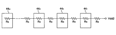
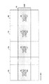
<電源配線>
図4は、本発明の発光ダイオード駆動回路における電流出力部441〜44m部分の半導体集積回路の一例の平面図を示す。同図中、電流出力部441〜44mはX方向に一列に並べて配置されている。梨地で示す電源配線50は電流出力部441〜44mの上をX方向に延在しており、電源Vdd2を電流出力部441〜44mに供給する。
<Power supply wiring>
FIG. 4 shows a plan view of an example of a semiconductor integrated circuit in the
電流出力部441〜44mそれぞれには、ハッチングで示すコンタクト領域511〜51mが設けられている。コンタクト領域511〜51mには電流出力部441〜44mそれぞれの抵抗R15〜R18を電源Vdd2に接続するためのコンタクトが設けられる。図4の等価回路は図5に示すようになる。図5において、Rxは電源配線50の配線抵抗である。
Each of the
この場合、電流出力部441〜44mのうちある電流出力部ではスイッチ36,38,40の全てがオンとなり、また、他の電流出力部ではスイッチ36,38,40のいずれかがオンとなり、各電流出力部441〜44mでスイッチ36,38,40のオンとなるパターンがそれぞれ異なる。このため、電流出力部441〜44mそれぞれで発生する電圧降下が異なり、電流出力部441〜44mそれぞれが駆動するLED451〜45mの駆動電流が安定しない、つまり、LED451〜45mの発光輝度が安定しない。
In this case, all of the
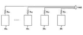
なお、図6に示すように、電流出力部441〜44mそれぞれに個別の電源配線521〜52mから電源Vdd2を供給することも考えられるが、個別の電源配線521〜52mを設ける領域が大幅に増加するため、実現性は極めて低い。図6において、Rx1〜Rxmは電源配線50の配線抵抗である。
As shown in FIG. 6, it is conceivable to supply the power supply Vdd2 from the individual power supply wirings 52 1 to 52m to the
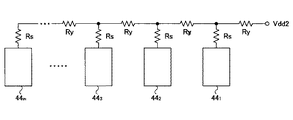
図7は、本発明の発光ダイオード駆動回路における電流出力部441〜44m部分の半導体集積回路の一実施形態の平面図を示す。同図中、電流出力部441〜44mはX方向に一列に並べて配置されている。梨地で示す電源配線50は電流出力部441〜44mの上にX方向に延在して配置されており、電源Vdd2を電流出力部441〜44mに供給する。
FIG. 7 shows a plan view of an embodiment of a semiconductor integrated circuit in the
電流出力部441〜44mそれぞれには、ハッチングで示すコンタクト領域511〜51mが設けられている。コンタクト領域511〜51mには電流出力部441〜44mそれぞれの抵抗R15〜R18を電源Vdd2に接続するためのコンタクトが設けられる。なお、コンタクト領域511〜51mの上部は電源配線50が設けられている。
Each of the
更に、コンタクト領域511〜51mそれぞれの周囲には、電源配線50を切り欠いたスリット部551〜55mが設けられ、コンタクト領域511〜51mはスリット部551〜55mによって一部(電流流入部)を開けて囲まれている。スリット部551〜55mはコンタクト領域511〜51mに流れ込む電流を制限するために設けられている。図7の等価回路は図8に示すようになる。図8において、Ryは電源配線50の配線抵抗、Rsはスリット部551〜55mによる等価的な制限抵抗である。なお、図7でスリット部551〜55mはコンタクト領域511〜51mの左側を開けて囲んでいるが、コンタクト領域511〜51mの右側または上側または下側を開けて囲む形状であっても良い。
Further, around the respective contact regions 51 1 ~51m, slit portions 55 1 ~55m formed by cutting the
このスリット部551〜55mを設けることにより、各電流出力部441〜44mでスイッチ36,38,40のオンとなるパターンがそれぞれ異なっても、電流出力部441〜44mに流れ込む電流が一定量以下に制限されるため、電流出力部441〜44mそれぞれで発生する電圧降下が制限される。
By providing this slit portion 55 1 ~55m, be different pattern which is turned on in the
これにより、電流出力部441〜44mそれぞれにおける電源電圧Vdd2を安定化することができる。基準電流部32の電源電圧Vdd1に対する電流出力部441〜44mそれぞれの電源電圧Vdd2が安定すると、電流出力部441〜44mそれぞれが駆動するLED451〜45mそれぞれの駆動電流が安定し、LED451〜45mの発光輝度が安定する。
Thereby, power supply voltage Vdd2 in each of the
なお、スリット部551〜55mは、コンタクト領域511〜51mの一部(電流流入部)を開けて囲むものであるが、どの部分を開けるかは自由に選定できる。 The slit portions 55 1 to 55 m open and surround a part (current inflow portion) of the contact regions 51 1 to 51 m, but any portion can be freely selected.
なお、MOSトランジスタM11〜M14が請求項記載の第1のカレントミラー回路に相当し、MOSトランジスタM14のドレイン電流が第1の電流に相当し、MOSトランジスタM15〜M18が第2のカレントミラー回路に相当し、MOSトランジスタM16のドレイン電流が第2の電流に相当し、MOSトランジスタM21〜M28が第3のカレントミラー回路に相当する。 The MOS transistors M11 to M14 correspond to the first current mirror circuit described in the claims, the drain current of the MOS transistor M14 corresponds to the first current, and the MOS transistors M15 to M18 correspond to the second current mirror circuit. The drain current of the MOS transistor M16 corresponds to the second current, and the MOS transistors M21 to M28 correspond to the third current mirror circuit.
30 演算増幅器
31 基準電圧源回路
32 基準電流部
33,35 電圧源
36,38,40 スイッチ
441〜44m 電流出力部
451〜45m LED
50 電源配線
511〜51m コンタクト領域
551〜55m スリット部
M11〜M28 MOSトランジスタ
R11〜R18,Ra,Rb 抵抗
Vdd1,Vdd2 電源
30
50 Power supply wiring 51 1 to 51 m Contact region 55 1 to 55 m Slit part M 11 to M 28 MOS transistors R 11 to R 18, Ra, Rb Resistance Vdd 1, Vdd 2 Power supply
Claims (4)
前記基準電流部は、前記基準電流が抵抗を流れることで発生する電圧が一定の基準電圧と同一となるよう前記基準電流を制御する演算増幅器と、
前記基準電流に基づく第1の電流を生成する第1のカレントミラー回路を有し、
各チャネルの前記電流出力部は、前記基準電流部の一部と共に構成され、前記第1の電流に基づく第2の電流を生成する第2のカレントミラー回路と、
前記第2の電流を供給され、前記複数系統のスイッチのうちオンとなったスイッチに対応して前記第2の電流に比例する電流を生成する第3のカレントミラー回路を有し、
前記第1、第2、第3のカレントミラー回路それぞれは、カスケード接続された2段のカレントミラー回路であることを特徴とする発光ダイオード駆動回路。 Light emission comprising a reference current section for generating a reference current and a current output section for a plurality of channels for generating on / off control of a plurality of system switches to generate a plurality of system drive currents proportional to the reference current and supplying them to a light emitting diode A diode drive circuit,
The reference current unit includes an operational amplifier that controls the reference current so that a voltage generated when the reference current flows through a resistor is the same as a constant reference voltage;
A first current mirror circuit that generates a first current based on the reference current;
The current output unit of each channel is configured together with a part of the reference current unit, and a second current mirror circuit that generates a second current based on the first current;
A third current mirror circuit that is supplied with the second current and generates a current proportional to the second current corresponding to a switch that is turned on among the plurality of systems of switches;
Each of the first, second, and third current mirror circuits is a cascade-connected two-stage current mirror circuit.
前記第1及び第3のカレントミラー回路を構成し高電圧側の電源に接続される各トランジスタと前記高電圧側の電源との間に抵抗を設けたことを特徴とする発光ダイオード駆動回路。 The light emitting diode drive circuit according to claim 1,
A light emitting diode driving circuit comprising a resistor provided between each of the transistors constituting the first and third current mirror circuits connected to a high voltage power source and the high voltage power source.
前記第2のカレントミラー回路を構成し低電圧側の電源に接続される各トランジスタと前記低電圧側の電源との間に抵抗を設けたことを特徴とする発光ダイオード駆動回路。 The light emitting diode drive circuit according to claim 1 or 2,
A light emitting diode driving circuit comprising a resistor provided between each of the transistors constituting the second current mirror circuit and connected to a low-voltage power supply and the low-voltage power supply.
前記複数チャネル分の電流出力部を一方向に並べて配置し、前記複数チャネル分の電流出力部の上に電源配線を前記一方向に延在させて配置し、
前記電源配線と各チャネルの前記電流出力部を接続する各チャネルのコンタクト領域の一部を開けて囲むよう前記電源配線を切り欠いたスリットを各チャネルに設けたことを特徴とする発光ダイオード駆動回路。 The light emitting diode drive circuit according to any one of claims 1 to 3,
The current output portions for the plurality of channels are arranged in one direction, and the power supply wiring is arranged to extend in the one direction on the current output portions for the plurality of channels,
A light emitting diode driving circuit, wherein a slit is formed in each channel so as to open and surround a part of a contact region of each channel connecting the power supply wiring and the current output portion of each channel. .
Priority Applications (3)
| Application Number | Priority Date | Filing Date | Title |
|---|---|---|---|
| JP2006188443A JP2008016732A (en) | 2006-07-07 | 2006-07-07 | Light-emitting diode driving circuit |
| CN2007800255352A CN101485003B (en) | 2006-07-07 | 2007-06-15 | Light emitting diode drive circuit |
| PCT/JP2007/062137 WO2008004426A1 (en) | 2006-07-07 | 2007-06-15 | Light emitting diode drive circuit |
Applications Claiming Priority (1)
| Application Number | Priority Date | Filing Date | Title |
|---|---|---|---|
| JP2006188443A JP2008016732A (en) | 2006-07-07 | 2006-07-07 | Light-emitting diode driving circuit |
Publications (1)
| Publication Number | Publication Date |
|---|---|
| JP2008016732A true JP2008016732A (en) | 2008-01-24 |
Family
ID=38894397
Family Applications (1)
| Application Number | Title | Priority Date | Filing Date |
|---|---|---|---|
| JP2006188443A Pending JP2008016732A (en) | 2006-07-07 | 2006-07-07 | Light-emitting diode driving circuit |
Country Status (3)
| Country | Link |
|---|---|
| JP (1) | JP2008016732A (en) |
| CN (1) | CN101485003B (en) |
| WO (1) | WO2008004426A1 (en) |
Cited By (1)
| Publication number | Priority date | Publication date | Assignee | Title |
|---|---|---|---|---|
| KR100986098B1 (en) | 2008-04-18 | 2010-10-07 | 창원대학교 산학협력단 | Parallel backlight LED driver |
Families Citing this family (1)
| Publication number | Priority date | Publication date | Assignee | Title |
|---|---|---|---|---|
| CN101694963B (en) * | 2009-09-22 | 2013-09-18 | 美芯晟科技(北京)有限公司 | High-precision low-voltage voltage/current switching circuit |
Citations (5)
| Publication number | Priority date | Publication date | Assignee | Title |
|---|---|---|---|---|
| JPH06328782A (en) * | 1993-05-26 | 1994-11-29 | Ricoh Co Ltd | Brightness controlling circuit device |
| JPH11251668A (en) * | 1998-02-27 | 1999-09-17 | Sony Corp | Circuit for driving light emitting element |
| JP2001308272A (en) * | 2000-04-19 | 2001-11-02 | Matsushita Electric Ind Co Ltd | Semiconductor integrated circuit device |
| JP2005183657A (en) * | 2003-12-19 | 2005-07-07 | Canon Inc | Light source driving circuit |
| JP2006054362A (en) * | 2004-08-13 | 2006-02-23 | Sanyo Electric Co Ltd | Led control circuit |
-
2006
- 2006-07-07 JP JP2006188443A patent/JP2008016732A/en active Pending
-
2007
- 2007-06-15 WO PCT/JP2007/062137 patent/WO2008004426A1/en active Application Filing
- 2007-06-15 CN CN2007800255352A patent/CN101485003B/en not_active Expired - Fee Related
Patent Citations (5)
| Publication number | Priority date | Publication date | Assignee | Title |
|---|---|---|---|---|
| JPH06328782A (en) * | 1993-05-26 | 1994-11-29 | Ricoh Co Ltd | Brightness controlling circuit device |
| JPH11251668A (en) * | 1998-02-27 | 1999-09-17 | Sony Corp | Circuit for driving light emitting element |
| JP2001308272A (en) * | 2000-04-19 | 2001-11-02 | Matsushita Electric Ind Co Ltd | Semiconductor integrated circuit device |
| JP2005183657A (en) * | 2003-12-19 | 2005-07-07 | Canon Inc | Light source driving circuit |
| JP2006054362A (en) * | 2004-08-13 | 2006-02-23 | Sanyo Electric Co Ltd | Led control circuit |
Cited By (1)
| Publication number | Priority date | Publication date | Assignee | Title |
|---|---|---|---|---|
| KR100986098B1 (en) | 2008-04-18 | 2010-10-07 | 창원대학교 산학협력단 | Parallel backlight LED driver |
Also Published As
| Publication number | Publication date |
|---|---|
| CN101485003A (en) | 2009-07-15 |
| CN101485003B (en) | 2011-07-20 |
| WO2008004426A1 (en) | 2008-01-10 |
Similar Documents
| Publication | Publication Date | Title |
|---|---|---|
| US6952083B2 (en) | Drive circuit for driving a current-driven display unit | |
| US7839097B2 (en) | System and method for wide-range high-accuracy-low-dropout current regulation | |
| JP3887229B2 (en) | Driving circuit for current-driven display device | |
| CN111065187B (en) | Current regulator | |
| US7436248B2 (en) | Circuit for generating identical output currents | |
| JP2007317933A (en) | Light-emitting diode drive circuit | |
| WO2007148581A1 (en) | Light emitting diode driving circuit | |
| JP6514946B2 (en) | Current driver circuit | |
| JP2008016732A (en) | Light-emitting diode driving circuit | |
| JP4792933B2 (en) | Current control circuit and LED driving semiconductor integrated circuit | |
| CN101473458B (en) | Light emitting diode driving circuit | |
| US20130093339A1 (en) | Driving circuits for light emitting elements | |
| JP2010074379A (en) | Driver circuit, and electronic circuit device | |
| JP5040185B2 (en) | Light emitting diode drive circuit | |
| JP2008218910A (en) | Light-emitting diode drive circuit | |
| JP2005135366A (en) | Current mirror circuit | |
| JP2008218911A (en) | Light-emitting diode drive circuit | |
| CN115148162B (en) | Drive circuit, backlight circuit and display panel | |
| JP2006216588A (en) | Light emitting element driving apparatus | |
| JP4983319B2 (en) | Light emitting diode drive circuit | |
| JP2019121969A (en) | Level shift device and IC device | |
| JPWO2023026919A5 (en) | ||
| KR100657152B1 (en) | Output driver for passive matrix organic light emitting diode | |
| JP2005114477A (en) | Load drive circuit | |
| JP2008310221A (en) | Current output device |
Legal Events
| Date | Code | Title | Description |
|---|---|---|---|
| A621 | Written request for application examination |
Free format text: JAPANESE INTERMEDIATE CODE: A621 Effective date: 20090327 |
|
| A131 | Notification of reasons for refusal |
Free format text: JAPANESE INTERMEDIATE CODE: A131 Effective date: 20120327 |
|
| A02 | Decision of refusal |
Free format text: JAPANESE INTERMEDIATE CODE: A02 Effective date: 20120918 |