JP2007538474A - Apparatus and method for tuning integrated circuit performance - Google Patents
Apparatus and method for tuning integrated circuit performance Download PDFInfo
- Publication number
- JP2007538474A JP2007538474A JP2007527379A JP2007527379A JP2007538474A JP 2007538474 A JP2007538474 A JP 2007538474A JP 2007527379 A JP2007527379 A JP 2007527379A JP 2007527379 A JP2007527379 A JP 2007527379A JP 2007538474 A JP2007538474 A JP 2007538474A
- Authority
- JP
- Japan
- Prior art keywords
- pld
- body bias
- programmable logic
- circuit
- logic device
- Prior art date
- Legal status (The legal status is an assumption and is not a legal conclusion. Google has not performed a legal analysis and makes no representation as to the accuracy of the status listed.)
- Pending
Links
Images


Classifications
-
- G—PHYSICS
- G06—COMPUTING; CALCULATING OR COUNTING
- G06F—ELECTRIC DIGITAL DATA PROCESSING
- G06F30/00—Computer-aided design [CAD]
- G06F30/30—Circuit design
- G06F30/34—Circuit design for reconfigurable circuits, e.g. field programmable gate arrays [FPGA] or programmable logic devices [PLD]
-
- H—ELECTRICITY
- H03—ELECTRONIC CIRCUITRY
- H03K—PULSE TECHNIQUE
- H03K5/00—Manipulating of pulses not covered by one of the other main groups of this subclass
- H03K5/13—Arrangements having a single output and transforming input signals into pulses delivered at desired time intervals
- H03K5/133—Arrangements having a single output and transforming input signals into pulses delivered at desired time intervals using a chain of active delay devices
-
- H—ELECTRICITY
- H03—ELECTRONIC CIRCUITRY
- H03K—PULSE TECHNIQUE
- H03K19/00—Logic circuits, i.e. having at least two inputs acting on one output; Inverting circuits
- H03K19/003—Modifications for increasing the reliability for protection
- H03K19/00369—Modifications for compensating variations of temperature, supply voltage or other physical parameters
-
- H—ELECTRICITY
- H03—ELECTRONIC CIRCUITRY
- H03K—PULSE TECHNIQUE
- H03K5/00—Manipulating of pulses not covered by one of the other main groups of this subclass
- H03K2005/00013—Delay, i.e. output pulse is delayed after input pulse and pulse length of output pulse is dependent on pulse length of input pulse
- H03K2005/00019—Variable delay
- H03K2005/00058—Variable delay controlled by a digital setting
-
- H—ELECTRICITY
- H03—ELECTRONIC CIRCUITRY
- H03K—PULSE TECHNIQUE
- H03K5/00—Manipulating of pulses not covered by one of the other main groups of this subclass
- H03K2005/00013—Delay, i.e. output pulse is delayed after input pulse and pulse length of output pulse is dependent on pulse length of input pulse
- H03K2005/0015—Layout of the delay element
- H03K2005/00156—Layout of the delay element using opamps, comparators, voltage multipliers or other analog building blocks
-
- H—ELECTRICITY
- H03—ELECTRONIC CIRCUITRY
- H03K—PULSE TECHNIQUE
- H03K2217/00—Indexing scheme related to electronic switching or gating, i.e. not by contact-making or -breaking covered by H03K17/00
- H03K2217/0018—Special modifications or use of the back gate voltage of a FET
Landscapes
- Engineering & Computer Science (AREA)
- Computer Hardware Design (AREA)
- Physics & Mathematics (AREA)
- General Engineering & Computer Science (AREA)
- Theoretical Computer Science (AREA)
- General Physics & Mathematics (AREA)
- Geometry (AREA)
- Evolutionary Computation (AREA)
- Computing Systems (AREA)
- Mathematical Physics (AREA)
- Nonlinear Science (AREA)
- Design And Manufacture Of Integrated Circuits (AREA)
- Logic Circuits (AREA)
- Pulse Circuits (AREA)
- Semiconductor Integrated Circuits (AREA)
Abstract
プログラマブルロジックデバイス(PLD)は、遅延回路およびボディバイアスジェネレータを含む。遅延回路は、PLDにおけるユーザー回路のインプリメントの遅延を表すように構成された遅延回路を有する。ボディバイアスジェネレータは、ユーザー回路内のトランジスタのボディバイアスを調整するように構成される。ボディバイアスジェネレータは、遅延回路の信号伝播遅延から引き出されたレベルに応答し、トランジスタのボディバイアスを調整する。A programmable logic device (PLD) includes a delay circuit and a body bias generator. The delay circuit has a delay circuit configured to represent the delay of the implementation of the user circuit in the PLD. The body bias generator is configured to adjust the body bias of the transistors in the user circuit. The body bias generator adjusts the body bias of the transistor in response to the level derived from the signal propagation delay of the delay circuit.
Description
(関連出願の相互参照)
本出願は、2004年5月19日出願の米国特許出願第10/848,953号、代理人整理番号第ALTR:026号の発明の名称「Apparatus and Methods for Adjusting the Performance of Programmable Logic Devices」の一部継続出願であり、それを参考として援用する。
(Cross-reference of related applications)
This application is a US Patent Application No. 10 / 848,953 filed on May 19, 2004, and is entitled “Apparatus and Methods for Adjusting the Program of Programmable Logic” of Alter No. ALTR: 026. This is a continuation-in-part application, which is incorporated by reference.
発明コンセプトは、一般に、プログラマブルロジックデバイス(PLD)を含む集積回路(IC)の性能の調整に関する。 The inventive concept generally relates to tuning the performance of an integrated circuit (IC) that includes a programmable logic device (PLD).
PLDは、設計者のみならずエンドユーザーにも柔軟性を提供するユビキタスな電子デバイスである。電子回路またはシステムの設計サイクル時、設計者は、設計ごとにPLDを単純に再プログラムすることによって、比較的多くの回数の設計反復を実行し得る。従って、設計サイクルの長さと費用は、他の代案と比較して減少する。同様に、エンドユーザーは、PLDを含む設計の機能性に対するコントロールの所望のレベルを有し得る。PLDを実地にまたはリアルタイムベースでさえプログラムすることによって、ユーザーは、回路またはシステムが動作する方法を変更し得る。 PLDs are ubiquitous electronic devices that provide flexibility to end users as well as designers. During the design cycle of an electronic circuit or system, a designer can perform a relatively large number of design iterations by simply reprogramming the PLD for each design. Thus, the length and cost of the design cycle is reduced compared to other alternatives. Similarly, the end user may have a desired level of control over the functionality of the design including the PLD. By programming the PLD on the ground or even on a real-time basis, the user can change the way the circuit or system operates.
ますます複雑化する設計を収容するため、現代のPLDは比較的多数のトランジスタを含む。さらにユーザーは、ますます高い性能を要求し、結果的に、より大きな動作周波数となる。その結果、PLDの消費電力、ワット損、ダイ温度、および従って、電力密度(種々の回路またはブロックのワット損)は、増加する傾向である。しかし、出力密度を上げていくと、PLDの設計とインプリメンテーションを非現実的または故障しやすくする。調整可能な消費電力および性能を特徴とするPLDに対する必要性が存在する。さらに、汎用IC内のトランジスタの性能(リーク、速度、およびワット損)を直接コントロールする必要性が存在する。 In order to accommodate increasingly complex designs, modern PLDs contain a relatively large number of transistors. In addition, users demand increasingly higher performance, resulting in higher operating frequencies. As a result, PLD power consumption, power dissipation, die temperature, and therefore power density (power dissipation of various circuits or blocks) tend to increase. However, increasing power density makes PLD design and implementation unrealistic or prone to failure. There is a need for a PLD characterized by adjustable power consumption and performance. Furthermore, there is a need to directly control the performance (leakage, speed, and power dissipation) of the transistors in a general purpose IC.
(要約)
開示された新しいコンセプトは、たとえば、速度と消費電力をトレードオフすることによって、PLDの性能を調整するための装置および方法に関する。発明のコンセプトの一局面は、PLDの性能を調整するための装置に関する。一実施形態において、ユーザーの回路をインプリメントするように構成されたPLDは、遅延回路およびボディバイアスジェネレータを含む。遅延回路は、PLDにおいてインプリメントされるユーザーの回路の遅延を表す遅延を有する。ユーザーの回路は、少なくとも一つのトランジスタを含む。ボディバイアスジェネレータは、遅延回路の伝播遅延から引き出された量に応答し、ユーザーの回路におけるトランジスタのボディバイアスを調整する。
(wrap up)
The new concept disclosed relates to an apparatus and method for adjusting the performance of a PLD, for example, by trading off speed and power consumption. One aspect of the inventive concept relates to an apparatus for adjusting the performance of a PLD. In one embodiment, a PLD configured to implement a user circuit includes a delay circuit and a body bias generator. The delay circuit has a delay that represents the delay of the user's circuit implemented in the PLD. The user's circuit includes at least one transistor. The body bias generator adjusts the body bias of the transistors in the user's circuit in response to the amount derived from the propagation delay of the delay circuit.
別の実施形態において、PLDは、基準トランジスタ、電流測定回路、およびボディバイアスジェネレータを含む。基準トランジスタは、PLD内の回路に関係する電流を供給する。電流測定回路は、基準トランジスタによって供給される電流を測定し、測定された電流信号をボディバイアスジェネレータに供給する。ボディバイアスジェネレータは、測定された電流信号から少なくとも一つのボディバイアス信号を引き出し、ボディバイアス信号をPLDの回路に供給する。 In another embodiment, the PLD includes a reference transistor, a current measurement circuit, and a body bias generator. The reference transistor supplies a current related to the circuit in the PLD. The current measurement circuit measures the current supplied by the reference transistor and supplies the measured current signal to the body bias generator. The body bias generator extracts at least one body bias signal from the measured current signal and supplies the body bias signal to the PLD circuit.
さらに別の実施形態において、PLDは、複数のユーザー回路および複数のボディバイアスジェネレータを含む。ユーザー回路の各々は、PLDにおいてインプリメントされる。複数のボディバイアスジェネレータの少なくとも一つは、ユーザー回路の少なくとも一つ内のトランジスタのボディバイアスを選択的に調整するように構成される。 In yet another embodiment, the PLD includes a plurality of user circuits and a plurality of body bias generators. Each user circuit is implemented in a PLD. At least one of the plurality of body bias generators is configured to selectively adjust a body bias of a transistor in at least one of the user circuits.
発明コンセプトの別の局面は、PLDの性能を調整し、ユーザーの回路をインプリメントするためにPLDを使用することの方法に関する。一実施形態において、電子回路をインプリメントするためにPLDを使用する方法は、設計を生成するために電子回路をPLD内の機能リソースにマッピングすること、および生成された設計の少なくとも一つの部分内の信号伝播遅延を表す遅延からボディバイアス値を引き出すことを含む。方法はさらに、生成された設計の部分内の少なくとも一つのトランジスタのボディバイアスレベルをボディバイアス値にプログラムすることを含む。 Another aspect of the inventive concept relates to a method of using the PLD to tune the performance of the PLD and implement the user's circuitry. In one embodiment, a method of using a PLD to implement an electronic circuit includes mapping the electronic circuit to a functional resource in the PLD to generate a design, and in at least one portion of the generated design. Deriving the body bias value from the delay representing the signal propagation delay. The method further includes programming a body bias level of at least one transistor in the portion of the generated design to a body bias value.
別の実施形態において、PLD内で実施される回路におけるトランジスタのリークレベルを調整する方法は、トランジスタのリーク電流を表す電流を得ること、および得られた電流からボディバイアスレベルを引き出すことを含む。方法はさらに、トランジスタのバイアスレベルを引き出されたボディバイアスレベルに調整することを含む。 In another embodiment, a method for adjusting the leakage level of a transistor in a circuit implemented in a PLD includes obtaining a current representative of the leakage current of the transistor and deriving a body bias level from the obtained current. The method further includes adjusting the bias level of the transistor to the derived body bias level.
さらに別の実施形態において、PLDにおける少なくとも一つの回路領域においてユーザー回路を実現する方法は、回路領域において少なくとも一つのトランジスタのボディバイアスレベルを選択し、PLD内における回路領域の初期配置を生成することを含む。方法はさらに、既存のボディバイアスレベルおよび配置が所定の性能基準を満たさない場合、回路領域においてトランジスタに印加されるべきボディバイアスレベルを少なくとも1回別のレベルに変更することを含む。 In yet another embodiment, a method for implementing a user circuit in at least one circuit region in a PLD selects a body bias level of at least one transistor in the circuit region and generates an initial arrangement of circuit regions in the PLD. including. The method further includes changing the body bias level to be applied to the transistor in the circuit region to another level at least once if the existing body bias level and arrangement does not meet the predetermined performance criteria.
添付の図面は、発明の例示的実施形態を示すに過ぎなく、従って、発明の範囲を制限するものと考えられるべきではない。本発明の記述からメリットを享受する当業者は、開示された発明のコンセプトがその他の等しく有効な実施形態に役立つことを理解する。図面において、二つ以上の図面において使用される同じ数字符号は、同じ、同様な、または同等な機能性、コンポーネント、またはブロックを示す。 The accompanying drawings only show exemplary embodiments of the invention and therefore should not be considered as limiting the scope of the invention. Those skilled in the art who have the benefit of the description of the invention understand that the disclosed inventive concept is useful in other equally valid embodiments. In the drawings, like reference numbers used in two or more drawings indicate the same, similar, or equivalent functionality, component, or block.
(詳細な説明)
本発明コンセプトは、調整可能な出力および性能を特徴とするPLDのための装置および関連方法を意図する。発明コンセプトは、従来のPLDが被っている過度の出力密度レベルを克服するのを助ける。さらに、本発明に従い、PLDの所望の部分またはすべての性能レベルを調整し得る(すなわち、個別のトランジスタからPLD全体に至るまでの範囲にわたる粒状ベースで)。
(Detailed explanation)
The inventive concept contemplates an apparatus and associated method for a PLD characterized by adjustable output and performance. The inventive concept helps to overcome the excessive power density levels experienced by conventional PLDs. Further, in accordance with the present invention, a desired portion or all performance levels of the PLD can be adjusted (ie, on a granular basis ranging from individual transistors to the entire PLD).
より具体的には、以下に詳細に記述されているように、発明コンセプトは、PLD内の個別のトランジスタまたはトランジスタのグループのボディバイアスまたはウェルバイアスの設定、プログラム、または調整を意図する。ボディバイアスを調整することは、トランジスタの消費電力および性能を変動させる。 More specifically, as described in detail below, the inventive concept contemplates setting, programming, or adjusting the body bias or well bias of individual transistors or groups of transistors within a PLD. Adjusting the body bias varies the power consumption and performance of the transistor.
この発明コンセプトは、従来のインプリメンテーション対して以下の利点を提供する。第1に、発明コンセプトは、性能と消費電力とのトレードオフ、または性能―消費電力のトレードオフの最適化を可能にする。第2に、PLDのクリティカル回路パスまたは部品において、必要に応じ、それらの性能を向上させるために、ボディバイアスレベルを選択的に設定し、プログラムし、または、調整し得る。逆に、非クリティカル回路パスまたはPLDのパーツにおいて、ボディバイアスレベルを選択的に設定し、プログラムし、または、調整し得、従って、それらの消費電力を減少させ、それらの出力密度を低下させ得る。 The inventive concept provides the following advantages over conventional implementations. First, the inventive concept allows optimization of the trade-off between performance and power consumption, or the performance-power consumption trade-off. Second, body bias levels can be selectively set, programmed, or adjusted to improve their performance in critical circuit paths or parts of the PLD as needed. Conversely, in non-critical circuit paths or PLD parts, body bias levels can be selectively set, programmed or adjusted, thus reducing their power consumption and reducing their power density .
さらに、PLD内で使用しない部品または回路を遮断または不能にし得、それによって、それらの消費電力を減少させ、それらの出力密度を低下させ得る。また、熱暴走を防ぐ(またはその可能性を減少させる)ために、発明コンセプトを採用し得る。より具体的には、従来のPLDにおいて、比較的高速で動作する回路は、より多くの電力を消費する傾向があり、その結果、PLDの温度上昇を招く。消費電力の増加は、これらの回路がさらに多くの電力を消費させる原因になり得る。このプラスのフィードバックメカニズムは、出力密度を不安全なまたは破壊的なレベルまで増加させ得る。 Furthermore, unused components or circuits in the PLD can be interrupted or disabled, thereby reducing their power consumption and reducing their power density. The inventive concept may also be employed to prevent (or reduce the possibility of) thermal runaway. More specifically, in a conventional PLD, a circuit that operates at a relatively high speed tends to consume more power, resulting in an increase in the temperature of the PLD. The increase in power consumption can cause these circuits to consume more power. This positive feedback mechanism can increase the power density to an unsafe or destructive level.
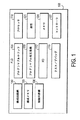
図1は、発明の例示的実施形態に従う、PLD103の汎用ブロック図を示す。PLD103は、構成回路網130、構成メモリ133、制御回路網136、プログラマブルロジック106、プログラマブル相互接続109、およびI/O回路網112を含む。さらに、PLD103は、必要に応じ、テスト/デバッグ回路網115、一つ以上のプロセッサ118、一つ以上の通信回路網121、一つ以上のメモリ124、一つ以上のコントローラ127を含み得る。
FIG. 1 shows a general block diagram of PLD 103, in accordance with an exemplary embodiment of the invention. PLD 103 includes
図1は、PLD103の簡略なブロック図を示すことに注意されたい。このように、PLD103は、当業者が理解するように、その他のブロックおよび回路網を含み得る。そのような回路網の例は、クロック発振および分配回路、冗長回路などを含む。さらに、PLD103は、必要に応じ、アナログ回路網、その他のディジタル回路網、および/または混合モード回路網を、含み得る。
Note that FIG. 1 shows a simplified block diagram of
プログラマブルロジック106は、ルックアップテーブル(LUT)、プロダクトタームロジック、マルチプレクサ、ロジックゲート、レジスタ、メモリなどの構成可能なロジック回路網またはプログラマブルロジック回路網のブロックを含む。プログラマブル相互接続109は、プログラマブルロジック106に結合し、プログラマブルロジック106内の種々のブロックとPLD103内または外部のその他の回路網との間の構成可能な相互接続(結合メカニズム)を提供する。
制御回路網136は、PLD103内の種々の動作を制御する。制御回路網136の監視の下に、PLD構成回路網130は、PLD103の機能性をプログラム、または、構成するために、構成データを使用する(PLD構成回路網は、そのデータをストレージデバイス、ホストなどの外部ソースから得る)。本発明の記述の助けをもって当業者が理解するように、構成データは、プログラマブルロジック106およびプログラマブル相互接続109をプログラムすることによって、PLD103の機能性を決定する。
The
本発明の記述のたすけを有する当業者が理解するように、I/O回路網は、幅広い様々のI/Oデバイスまたは回路を構成する。I/O回路網112は、PLD103の種々の部品、たとえば、プログラマブルロジック106およびプログラマブル相互接続109など、に接続する。I/O回路112は、外部回路またはデバイスと通信するために、PLD103内の種々のブロック用の機構および回路網を提供する。
As will be appreciated by those skilled in the art having the description of the invention, the I / O circuitry comprises a wide variety of I / O devices or circuits. I /
テスト/デバッグ回路網115は、PLD103内の種々のブロックおよび回路のテストおよびトラブルシューティングを容易にする。テスト/デバッグ回路網115は、本発明の記述のたすけを有する当業者に知られている種々のブロックまたは回路を含み得る。たとえば、テスト/デバッグ回路網115は、必要に応じ、PLD103のパワーアップまたはリセット後のテストを実行する回路を含み得る。テスト/デバッグ回路網115はまた、必要に応じ、コーディングおよびパリティ回路も含む。
Test /
上記されるように、PLD103は、一つ以上のプロセッサ118を含み得る。プロセッサ118は、PLD103内のその他のブロックおよび回路に結合し得る。本発明の記述のたすけをもって当業者が理解するように、プロセッサ118は、PLD103内のまたは外部の回路からデータおよび情報を受け取り得、幅広い様々の方法で情報を処理し得る。一つ以上のプロセッサ118は、ディジタル信号プロセッサ(DSP)を構成し得る。DSPは、必要に応じ、圧縮、圧縮解除、音声処理、映像処理、フィルタリングなどの幅広い様々の信号処理タスクの実行を可能にする。
As described above,
PLD103はまた、一つ以上の通信回路網121も含み得る。本発明の記述からメリットを享受する当業者は理解するように、通信回路網121は、PLD103内の種々の回路とPLD103の外部の回路との間のデータおよび情報の交換を容易にし得る。一例として、通信回路網121は、必要に応じ、種々のプロトコル機能性(たとえば、伝送制御プロトコル/インターネットプロトコル(TCP/IP)、ユーザデータグラムプロトコル(UDPなど)を提供し得る。別の例として、通信回路網121は、必要に応じ、ネットワーク(たとえば、イーサネット(登録商標)、トークンリングなど)またはバスインターフェース回路網を含み得る。
PLD103はさらに、一つ以上のメモリ124および一つ以上のコントローラ127を含み得る。メモリ124は、PLD103内の種々のデータおよび情報(ユーザーデータ、中間結果、計算結果など)の格納を可能にする。メモリ124は、必要に応じ、粒状形またはブロック形を有し得る。コントローラ127は、PLDの外部の回路網の動作および種々の機能にインタフェースし、制御することを可能にする。たとえば、コントローラ127は、必要に応じ、外部の同期ダイナミックランダムアクセスメモリ(SDRAM)にインタフェースし、制御するメモリコントローラを構成し得る。
The
PLD103内の回路網のブロックは、多数のトランジスタを含む。より具体的には、トランジスタは、必要に応じ、n型MOS(NMOS)、p型MOS(PMOS)、相補型MOS(CMOS)、または、部分空乏シリコンオンインシュレータ(SOI)MOSトランジスタ(またはこれらの種類のトランジスタの組み合せ)などの金属酸化物半導体(MOS)トランジスタを構成する。
57 図2は、本発明に従う、例示的な実施形態において使用されるMOSトランジスタを示す。MOSトランジスタは、本体(または基板)領域203、ソース領域206、ドレイン領域209、ゲートインシュレータ215、およびゲート212を含む。動作の飽和領域におけるMOSトランジスタのドレイン電流は、トランジスタの閾値電圧およびゲートからソースへの電圧に依存し、
iD=K(νGS−VT)2 (1)
である。ここで、
iD=全ドレイン電流(すなわち、ACおよびDC成分を含む)
K=定数
νGS=ゲートからソースへの全電圧(すなわち、ACおよびDC成分を含む)、および
VT=閾値電圧
である。
The network block within the
FIG. 2 shows a MOS transistor used in an exemplary embodiment according to the present invention. The MOS transistor includes a main body (or substrate)
i D = K (ν GS −V T ) 2 (1)
It is. here,
i D = total drain current (ie including AC and DC components)
K = constant ν GS = total voltage from gate to source (ie, including AC and DC components), and V T = threshold voltage.
閾値電圧VTは、トランジスタのソース領域206と本体領域203との間の電圧などの多数の要因に依存する。下記の等式は、本体からソースへの電圧の関数としての閾値電圧を提供する:
The threshold voltage V T depends on a number of factors such as the voltage between the

VT(0)=ソースから本体(または本体からソース)への電圧が0にセットされた閾値電圧
γ=本体係数で、本体のドーピングレベルに依存する定数
ΦF=定数
νBS=本体からソースへの全電圧(すなわち、ACおよびDC成分を含む)、および
νSB=ソースから本体への全電圧(すなわち、ACおよびDC成分を含む)
である。本体からソースへの電圧、νBS(または、ソースから本体への電圧、νSB)が0に等しいとき、閾値電圧VTは、VT(0)に等しいことに注意されたい。
V T (0) = threshold voltage γ = body coefficient with source-to-body (or body-to-source) voltage set to 0, constant Φ F = constant ν BS = body to source depending on body doping level Total voltage to (ie, including AC and DC components), and ν SB = total voltage from source to body (ie, including AC and DC components)
It is. Note that when the body-to-source voltage, ν BS (or source-to-body voltage, ν SB ) is equal to 0, the threshold voltage V T is equal to V T (0) .
等式2Bが示すように、有限本体係数γに関して、ソースから本体への電圧、νSB、が増加すると、トランジスタの閾値電圧は増加する。しかし、等式(1)は、特定のゲートからソースへの電圧に関して、閾値電圧における増加は、トランジスタのドレイン電流iDを減少させることを示す。換言すると、等式1および2Bに従って、定数のゲートからソースへの電圧νGSに関して、ソースから本体への電圧νSBにおける増加は、閾値電圧、VTにおける増加の原因になる。
As equation 2B shows, for a finite body factor γ, as the source-to-body voltage, ν SB , increases, the threshold voltage of the transistor increases. However, equation (1) shows that for a particular gate-to-source voltage, an increase in threshold voltage decreases the drain current i D of the transistor. In other words, according to
増加した閾値電圧VTは、今度は、量(νGS―VT)における減少の原因となり、その結果、トランジスタのドレイン電流iDにおける減少となる。このように、ゲートからソースへの一定の電圧νGSに関して、ソースから本体への電圧νSBにおける増加は、トランジスタの電流駆動能力(性能の一つの基準)における減少の原因となる。トランジスタの減少した電流駆動能力は、今度は、回路動作を遅くすることになり、最終的には、トランジスタを含むPLDの動作を遅くする。 The increased threshold voltage V T in turn causes a decrease in the quantity (ν GS −V T ), resulting in a decrease in the transistor drain current i D. Thus, for a constant voltage ν GS from the gate to the source, an increase in the source to body voltage ν SB causes a decrease in the current drive capability (one measure of performance) of the transistor. The reduced current drive capability of the transistor will in turn slow down the circuit operation and ultimately slow down the operation of the PLD containing the transistor.
トランジスタのワット損もまた、その閾値電圧における変化に従って、変動する。より具体的には、閾値電圧が小さくなると、トランジスタのOFF状態のリーク電流(Ioff)が増加する。逆もまた同様である。トランジスタのIoffは、そのスタティック(非スイッチング)のワット損に影響する。さらに、より小さい閾値電圧は、トランジスタのダイナミックまたはスイッチングワット損を増加させる。このように、ボディバイアスを調整することによって閾値電圧を変化させると、MOSトランジスタのワット損に影響する。 The power dissipation of a transistor also varies with changes in its threshold voltage. More specifically, when the threshold voltage decreases, the leakage current (I off ) of the transistor in the OFF state increases. The reverse is also true. A transistor's I off affects its static (non-switching) power dissipation. In addition, smaller threshold voltages increase transistor dynamic or switching power dissipation. Thus, changing the threshold voltage by adjusting the body bias affects the power dissipation of the MOS transistor.
さらに、所定の供給電圧、VDD、に関して、閾値電圧、VT、における増加は、トランジスタがパストランジスタとして動作するときに、トタンジスタが伝導し得る最大電圧を制限する。換言すると、閾値電圧、VT、が、ゲートからソースへの電圧νGSに等しいかまたは超える点まで増加する場合、ドレイン電流は0に減少する。このように、トランジスタのドレインに印加される電圧、たとえば、ロジック1レベルに対応する電圧は、トランジスタのソースに適切に伝導しない。その結果、トランジスタは、パストランジスタとして信頼性をもって動作しない。
Furthermore, for a given supply voltage, V DD , the increase in threshold voltage, V T , limits the maximum voltage that the transistor can conduct when the transistor operates as a pass transistor. In other words, if the threshold voltage, V T , increases to a point equal to or exceeding the gate-to-source voltage ν GS , the drain current decreases to zero. Thus, a voltage applied to the drain of the transistor, eg, a voltage corresponding to a
上記に示すように、MOSトランジスタのボディバイアス、従ってトランジスタのソースから本体への電圧を調整することによって、MOSトランジスタの性能に影響を及ぼし得る(最終的には、閾値電圧における変化の結果を招く)。ボディバイアスを調整すると、電流駆動能力、動作速度、ワット損、などの性能基準に影響する。 As indicated above, adjusting the body bias of the MOS transistor, and hence the voltage from the source to the body of the transistor, can affect the performance of the MOS transistor (which ultimately results in a change in threshold voltage ). Adjusting the body bias affects performance criteria such as current drive capability, operating speed, and power dissipation.
上記のように、発明に従う実施形態において、必要に応じ、PLD内の個々のトランジスタ、個々の回路またはブロック、トランジスタまたはブロックのグループ、またはPLD全体までのボディバイアスを調整し得る。さらに、必要に応じ、個々のNMOSおよびPMOSトランジスタのボディバイアス、または、NMOSおよびPMOSトランジスタのグループのボディバイアスを調整し得る。以下の説明は、詳細を提供する。 As described above, in embodiments according to the invention, the body bias across individual transistors, individual circuits or blocks, groups of transistors or blocks, or the entire PLD may be adjusted as needed. Furthermore, the body bias of individual NMOS and PMOS transistors or a group of NMOS and PMOS transistors can be adjusted as needed. The following description provides details.
図3は、発明の例示的実施形態に従うPLD103の平面図を示す。PLD103は、二次元アレイとして配置されているプログラマブルロジック106を含む。水平相互接続および垂直相互接続として配置されたプログラマブル相互接続109は、プログラマブルロジック106のブロックを互いに結合する。必要に応じ、プログラマブルロジック106の各ブロック、プログラマブル相互接続109の各セグメント、またはその両方のボディバイアスを調整し得る。さらに、必要に応じ、プログラマブルロジック106の一つ以上のブロックの部分、プログラマブル相互接続109の部分、またはその両方のボディバイアスを調整し得る。
FIG. 3 shows a top view of the
例示的実施形態において、発明に従うPLDは、階層アーキテクチャを有する。換言すると、図3のプログラマブルロジック106の各ブロックは、今度は、より小さいかまたはより多い粒状のプログラマブルロジクブロックまたは回路を含み得る。必要に応じ、PLDの階層アーキテクチャの各レベルにおけるトランジスタのボディバイアスを調整し得る。
In an exemplary embodiment, the PLD according to the invention has a hierarchical architecture. In other words, each block of the
図4は、発明の例示的な実施形態に従うPLDにおけるプログラマブルロジック106のブロック図を示す。プログラマブルロジック106は、論理要素またはプログラマブルロジック回路250、ローカル相互接続253、インタフェース回路256およびインタフェース回路259を含む。本発明の記述からメリットを享受する当業者は理解するように、論理要素250は、構成可能なロジック機能またはプログラマブルロジック機能、たとえば、LUT、レジスタ、プロダクトタームロジックなどを提供する。ローカル相互接続253は、必要に応じ、論理要素250が互いにまたはプログラマブル相互接続109(「グローバル相互接続」と呼ばれることがある)に結合するように構成可能なメカニズムまたはプログラマブルメカニズムを提供する。
FIG. 4 shows a block diagram of
インタフェース回路256およびインタフェース回路259は、回路網のプログラマブルロジック106がプログラマブル相互接続109(および従って、図3に示すように、その他のプログラマブルロジック106)に結合するように、構成可能な方法またはプログラマブルな方法を提供する。本発明の記述からメリットを享受する当業者は理解するように、インタフェース回路256およびインタフェース回路259は、マルチプレクサ(MUX)、レジスタ、バッファ、ドライバなどを含み得る。
必要に応じ、PLD103(図1、図3、および図4を参照)内の回路網の各部分またはブロックのボディバイアスを調整し得る。さらに、必要に応じ、個々または集合的ベースで、回路網の各部分またはブロックのボディバイアスを他に無関係に調整し得る。回路網の各部分またはブロック内で、必要に応じ、個々または集合的ベースで、各サブブロックまたはトランジスタのボディバイアス、またはサブブロックまたはトランジスタのグループのボディバイアスを調整し得る。 If necessary, the body bias of each portion or block of circuitry within the PLD 103 (see FIGS. 1, 3 and 4) may be adjusted. In addition, the body bias of each part or block of the network can be adjusted independently or otherwise, as needed, on an individual or collective basis. Within each portion or block of the network, the body bias of each sub-block or transistor or group of sub-blocks or transistors can be adjusted on an individual or collective basis as needed.
たとえば、発明の例示的な実施形態に従い、PLD内の下記の回路網のすべてまたは部分のボディバイアスを調整し得る:図1の一つ以上のブロック(たとえば、プログラマブルロジック106、プログラマブル相互接続109など);一つ以上のプログラマブルロジックブロック106内の一つ以上の論理要素250;一つ以上のプログラマブルロジックブロック106内の一つ以上のインタフェース回路256および/または259;一つ以上のプログラマブルロジック106内の一つ以上のローカル相互接続;および一つ以上のインタフェース回路256および/または259内の一つ以上のMUX、ドライバ、バッファなど。
For example, according to an exemplary embodiment of the invention, the body bias of all or part of the following circuitry in the PLD may be adjusted: one or more blocks of FIG. 1 (eg,
上記のとおり、ボディバイアス調整を、粒状度の任意の所望レベルで、行い得る。換言すると、必要また適用可能に応じ、個々のトランジスタ、トランジスタのグループ、サブブロック、ブロックまたはPLD全体に適用可能な調整を行い得る。たとえば、必要に応じ、一つ以上のNMOSトランジスタのボディバイアス調整を、一つ以上のPMOSトランジスタに無関係に、行い得る。 As described above, body bias adjustments can be made at any desired level of granularity. In other words, adjustments applicable to individual transistors, groups of transistors, sub-blocks, blocks or entire PLDs may be made as needed and applicable. For example, if necessary, the body bias adjustment of one or more NMOS transistors can be performed independently of one or more PMOS transistors.
さらに、必要に応じ、PLD103内の一つの要素のボディバイアスを、その他のすべての要素に無関係に、調整し得る。本発明の記述からメリットを享受する当業者は理解するように、必要に応じ、PLDのいくつかの部品のボディバイアス調整を行い得、さらにPLDのその他の部品の固定またはデフォルトのボディバイアスを提供し得る。
Furthermore, if necessary, the body bias of one element in the
ボディバイアス調整の粒状度の例として、2入力、1出力のMUXを考慮されたい。図5は、ボディバイアス調整を含む発明の例示的実施形態に従うPLDにおいて使用されるMUXを示す。MUXは、トランジスタ275およびトランジスタ278を含む。MUXは、回路Aから信号を受信し、別の信号を回路Bから受信する。選択信号、S、およびそのコンプリメントS’に応答し、MUXは、回路Aまたは回路Bのいずれかからの信号を回路C(MUXの出力に結合された)に伝送する。
As an example of the granularity of body bias adjustment, consider a 2-input, 1-output MUX. FIG. 5 shows a MUX used in a PLD according to an exemplary embodiment of the invention that includes body bias adjustment. The MUX includes a
トランジスタ275およびトランジスタ278のボディバイアスは多数の方法で調整し得る。第1に、ボディバイスを調整しないことを選択し得る(たとえば、PLD内のデフォルトボディバイアスを使用する)。第2に、トランジスタ275のボディバイアスをトランジスタ278のボディバイアスと同レベルに調整し得る。代案として、トランジスタ275およびトランジスタ278のみのボディバイアスを調整し得る。別の選択として、トランジスタ275およびトランジスタ278の各々のボディバイアスを個々に調整し得る。
The body bias of
従って、MUXの性能特性を柔軟性ある方法で構成し得る。他の方法では、MUXの動作速度、電流駆動能力、およびワット損のバランスまたはトレードオフを、互いに対して、行い得る。さらなる例として、ボディバイアス調整コンセプトを、MUXのトランジスタの一セット、特定の信号ルート(たとえば、特定の入力に対応した信号伝送ルーティング)、パストランジスタの一セット(たとえば、プログラマブルルーティングにおけるパストランジスタ一セットで、それが、構成メモリビット数を節約するためにその他のパストランジスタのセットによって共有されたMUXに入力する)、などに広げ得ることに注意されたい。 Therefore, the performance characteristics of the MUX can be configured in a flexible way. In other ways, a balance or trade-off of MUX operating speed, current drive capability, and power dissipation can be made to each other. As a further example, the body bias adjustment concept can be applied to a set of MUX transistors, a specific signal route (eg, signal transmission routing corresponding to a specific input), a set of pass transistors (eg, a set of pass transistors in programmable routing). Note that it can be extended to a MUX shared by a set of other pass transistors to save configuration memory bits.
上記のとおり、ユーザーは、本発明に従い、PLDの種々の部分のボディバイアスを調整し得る。ユーザーは、PLDの設計をマッピングするために使用されるソフトウェアを使用することによって、そのように行い得る。図6Aは、発明の例示的実施形態に従うPLDコンピュータ支援設計(CAD)ソフトウェアが使用する種々のソフトウェアモジュールを示す。モジュールは、設計入力モジュール305、合成モジュール310、プレース・ルートモジュール315、および検査モジュール320を含む。
As described above, the user can adjust the body bias of various portions of the PLD in accordance with the present invention. The user may do so by using software that is used to map the PLD design. FIG. 6A shows various software modules used by PLD computer-aided design (CAD) software according to an exemplary embodiment of the invention. The module includes a
設計入力(design−entry)モジュール305は、多様な設計ファイルの統合を可能にする。ユーザーは、必要に応じ、設計入力モジュール305を使用することによってまたは種々の電子設計オートメーション(EDA)またはCADツール(業界標準のEDAツールなど)を使用することによって、設計ファイルを生成し得る。ユーザーは、必要に応じ、グラフ形式、波形ベース形式、スケマティック形式で、テキストまたはバイナリ形式で、またはこれらの形式の組み合わせで、設計を入力し得る。
A design-
合成モジュール310は、設計入力モジュール305の出力を受け取る。ユーザー提供の設計に基づき、合成モジュール310は、ユーザー提供の設計を実現する適切なロジック回路網を生成する。一つ以上のPLD(明白には示されてない)は、合成された全体設計またはシステムを実行する。合成モジュール310はまた、ユーザーの設計における種々のモジュールの統合および適切な動作およびインタフェースを可能にする任意のグルー(glue)ロジックも生成し得る。たとえば、合成モジュール310は、一つのブロックの出力が別のブロックの入力と適切にインタフェースするように、適切なハードウェアを提供する。合成モジュール310は、全体設計またはシステムにおいてモジュールの各々の仕様に合致するように、適切なハードウェアを提供する。
The
さらに、合成モジュール310は、合成された設計を最適化するためのアルゴリズムおよびルーチンを含み得る。最適化によって、合成モジュール310は、全体設計またはシステムを実行する一つ以上のPLDのリソースをより効率的に使用するよう努める
。合成モジュール310は、プレース・ルートモジュール315への出力を提供する。
Further, the
プレース・ルートモジュール315は、最適なロジックマッピングおよび配置を行うため、設計者のタイミング仕様を使用する。ロジックマッピングおよび配置は、PLD内のルーティングリソースの使用を決定する。換言すると、設計の所定の部品のためにPLDとの特定のプログラマブル相互接続を使用することによって、プレース・ルートモジュール315は、全体設計またはシステムの性能の最適化を支援する。PLDルーティングリソースを適切に使用することによって、プレース・ルートモジュール315は、全体設計またはシステムのクリティカルタイミングパスを満たすように支援する。プレース・ルートモジュール315は、本発明の記述からメリットを享受する当業者に知られている方法より速く、クリティカルタイミングパスを最適化し、タイミング閉止の提供を支援する。その結果、全体設計またはシステムは、より速い性能(すなわち、より高いクロックレイトまたはより高いスループットでの動作)を達成し得る。
The place /
さらに、プレース・ルートモジュール315は、設計およびシステムを実行するPLDの部分またはすべてのボディバイアスを調整する。プレース・ルートモジュール315は、それを自動的に行うか、ユーザー指定の基準に従って行うか、またはその二つの組み合わせに従って、行い得る。プレース・ルートモジュール315は、ユーザー指定の基準(たとえば、ワット損、速度、および/または電流駆動能力などの性能仕様)を使用し得る。さらに、または、その代わりに、プレース・ルートモジュール315は、必要に応じ、設計またはシステムのパーツまたはすべてのボディバイアスを調整するために、設計またはシステム内のクリティカルパスに関する情報を使用し得る。
In addition, the
たとえば、プレース・ルートモジュール315は、より高い性能を達成するために、設計またはシステムのクリティカルパーツのボディバイアスを調整し得る。プレース・ルートモジュール315は、必要に応じ、パワーおよび性能のトレードオフを行うために、ワット損基準(たとえば、最大出力密度)を考慮に入れ得る。プレース・ルートモジュール315は、検査モジュール320に対する最適な設計を提供する。
For example, the
検査モジュール320は、設計のシミュレーションおよび検査を実行する。シミュレーションおよび検査は、設計がユーザーの規定した仕様に従うことを検査することをその一部において努める。シミュレーションおよび検査はまた、設計を試作する前に、すべての設計問題を検出し、修正することを意図する。このように、検査モジュール320は、ユーザーが全体設計またはシステムの総コストを削減し、市場へ出すまでの時間を短縮するよう支援する。
The
検査モジュール320は、必要に応じ、種々の検査およびシミュレーションオプションを支持し、実行し得る。オプションは、必要に応じ、設計規則チェック、機能上の検査、テストベンチ(test−bench)生成、スタティックタイミング解析、タイミングシミュレーション、ハードウェア/ソフトウェアシミュレーション、システム内検査、ボードレベル(board−level)タイミング解析、信号の完全性分析および電磁環境適合性(EMC)、形式的なネットリスト検査、および消費電力推定を含み得る。必要に応じ、また本発明の記述からメリットを享受する当業者は理解するように、他のまたは追加の検査技術が実行し得ることに注意されたい。上記のとおり、発明に従うPLDアーキテクチャおよび回路網は、ユーザーが、PLDまたはPLDの領域において、速度を犠牲にしてリーク(および従って、ワット損)に対処できる能力を提供する。ユーザーがこの機能性を使用することをできるだけ便利にするために、発明の例示的実施形態に従うPLD CADは、ユーザーの仕様と基準を自動的に満たすように、回路網を自動的に構成し得る。さらに、ユーザーの回路への速度への影響を最小にしながらリーク減少を最大にするため、発明の種々な実施形態に従うPLD CADは、ユーザー回路のインプリメンテーション時にバイアス領域の存在を考慮し、バイアス領域の有効性を最大にするように回路を最適化する。以下の説明は、PLD CADの機能性の詳細を提供する。
基板バイアスを最高に活用するタイミング駆動のPLD CADシステムに関して、設計インプリメンテーション時に、そのシステムが、PLDまたはPLDの各領域(一つ以上のトランジスタを含み得る)に対して基板バイアスを推定すべきである。PLD CADは、設計のタイミング分析時にボディバイアスを考慮に入れる。このように、ボディバイアスレベルは、タイミングの観点から設計のどの部分がクリティカルになるかについて影響する。 For timing-driven PLD CAD systems that take full advantage of substrate bias, during design implementation, the system should estimate the substrate bias for each PLD or region of the PLD (which may include one or more transistors). It is. PLD CAD takes into account body biases during design timing analysis. Thus, the body bias level affects which part of the design becomes critical from a timing perspective.
最初、CADシステムは、ユーザーが一つ以上のトランジスタのボディバイアスレベルの設定またはプログラムを望むPLDの各領域に対して、あるボディバイアスレベル(および従って、リーク/速度設定)を想定する。一つの可能性ある選択として、PLD CADは、すべての影響を受けた領域が比較的低速度設定(すなわち、比較的低リークレベルの結果となるボディバイアス)を使用すると想定し得る。PLD CADシステムは、PLD回路網の初期配置を提供する。配置は、その初期配置の反復の改善によって、進行する。 Initially, the CAD system assumes a certain body bias level (and hence leakage / speed setting) for each region of the PLD that the user desires to set or program the body bias level of one or more transistors. As one possible choice, the PLD CAD may assume that all affected regions use a relatively low speed setting (ie, body bias that results in a relatively low leak level). The PLD CAD system provides an initial placement of the PLD network. Placement proceeds by improving the initial placement iterations.
この反復の改善手順の種々の時点において、PLD CADは、回路の速度を推定し、関係するすべての接続に対してタイミングスラック値を計算する。タイミングスラック値の計算は、遅延を推定するときに、各領域に対して選ばれた現在のボディバイアスレベルを考慮に入れる。PLD CADは、ボディバイアス選択を配置の反復の改善にインタリーブすることに注意されたい。PLD CADは、より高速な(および対応するより高いリークの)ボディバイアス設定への変換のため、より小さい平均および最悪ケースの接続スラック値を有する回路の部分を含む領域を評価する。CADソフトウェアは、一つ以上の領域について新候補バイアス設定を選択し、回路タイミングの点から新設定の総原価、ならびにリーク電流および/または漏れ電力における全増加を推定することによって、バイアス設定を評価する。新バイアス設定が、領域におけるすべての接続についてプラスのスラック値に導く場合(または、領域におけるより少ないマイナススラックレベル)、PLD CADは、一般に、新バイアス設定を採用する。 At various points in this iterative improvement procedure, the PLD CAD estimates the speed of the circuit and calculates timing slack values for all relevant connections. The timing slack value calculation takes into account the current body bias level chosen for each region when estimating the delay. Note that PLD CAD interleaves body bias selection with improved placement iterations. The PLD CAD evaluates the region containing the portion of the circuit that has a smaller average and worst case connection slack value for conversion to a faster (and corresponding higher leakage) body bias setting. The CAD software evaluates the bias settings by selecting new candidate bias settings for one or more regions and estimating the total cost of the new settings and the total increase in leakage current and / or leakage power in terms of circuit timing. To do. If the new bias setting leads to a positive slack value for all connections in the region (or less negative slack level in the region), the PLD CAD generally employs the new bias setting.
同様に、CADソフトウェアは、より低速度のボディバイアス設定への変換のために、現在比較的高いバイアス設定を有する領域で、すべての接続がプラスのスラック値を有する領域を評価する。新ボディバイアス採用することが、どの回路タイミング基準に対しても違反を引き起こすことにならない場合、CADソフトウェアは、新ボディバイアス設定を採用する。 Similarly, CAD software evaluates areas where all connections have positive slack values in areas that currently have relatively high bias settings for conversion to lower speed body bias settings. If adopting a new body bias does not cause a violation of any circuit timing criteria, the CAD software adopts a new body bias setting.
一つ以上のバイアス設定を変更次第、反復配置改善は、変更されたバイアス設定によって発生するすべての起こりうるタイミングの懸念または違反を解決する試みを継続し、または、よりタイムクリティカルな回路網をより高速度を有する新しく作成されたバイアス領域に移動するよう試みる。配置とルーティングがユーザーのタイミングおよびパワー目標を満たすときか、または、所望または所定の反復限界に達した(それ以上の改善がなされ得ないように見える)のいずれかのとき、アルゴリズムは終了する。 As soon as one or more bias settings are changed, iterative placement improvements will continue to attempt to resolve all possible timing concerns or violations caused by the changed bias settings, or make more time-critical circuitry more Attempt to move to a newly created bias region with high velocity. The algorithm ends when placement and routing meet the user's timing and power goals, or when the desired or predetermined iteration limit has been reached (it seems that no further improvement can be made).
図6Bは、発明の例示的実施形態に従うPLD CADソフトウェアの流れ図を示す。図6Bに示されるPLD CADは、PLDの各領域に対するボディバイアスの選択をタイミング駆動のプレース・ルートCADシステムに組み入れる。 FIG. 6B shows a flow diagram of PLD CAD software according to an exemplary embodiment of the invention. The PLD CAD shown in FIG. 6B incorporates body bias selection for each region of the PLD into a timing driven place-route CAD system.
より具体的には、330において、PLD CADは、初期領域ボディバイアス設定をセットする。335において、ソフトウェアは初期配置を生成する。次に、338において、ソフトウェアは、現在のボディバイアス設定を反映する遅延推定を使用して、回路網のタイミングを分析する。341において、ソフトウェアは、ユーザーのタイミングおよびパワー目標を満たしたかどうかについて判断する。満たしたと判断する場合、344において、ソフトウェアは、配置およびボディバイアス選択を記録する。満たさなかったと判断する場合、ソフトウェアは、347において、反復限界に達したかどうかをチェックし判断する。達したと判断する場合、ソフトウェアは、344に進み、現在の配置およびボディバイアス選択を記録する。ソフトウェアが反復限界に達していない場合、ソフトウェアは、反復カウント(明白には示されていない)をインクリメントし、350において、少なくともいくつかの領域のバイアス設定を変更する。353において、ソフトウェアは、変更されたボディバイアス設定を反映する遅延推定を使用して回路網のタイミングを分析する。356において、ソフトウェアは、回路の配置を改善し、341に飛び、ユーザーのタイミングおよびパワー目標を満たしたかどうかを判断する。 More specifically, at 330, the PLD CAD sets the initial region body bias setting. At 335, the software generates an initial configuration. Next, at 338, the software analyzes the network timing using a delay estimate that reflects the current body bias setting. At 341, the software determines whether the user's timing and power goals have been met. If so, at 344, the software records the placement and body bias selection. If it is determined that it has not been met, the software checks and determines at 347 whether the iteration limit has been reached. If so, the software proceeds to 344 and records the current placement and body bias selection. If the software has not reached the iteration limit, the software increments the iteration count (not explicitly shown) and changes the bias setting of at least some regions at 350. At 353, the software analyzes the network timing using a delay estimate that reflects the changed body bias setting. At 356, the software improves circuit placement and jumps to 341 to determine if the user's timing and power goals have been met.
本発明の記述からメリットを享受する当業者は理解するように、本明細書に記述されたアルゴリズムの多くの変種を使用し得る。たとえば、すべての領域を低速または高速に設定するなど、種々の初期ボディバイアスの設定を使用し得る。ソフトウェアが、配置におけるすべてのタイミング仕様を満たすと推定する場合、より大きなプラススラック値を有する接続を含む領域を優先して、高速バイアス領域を低速領域への変換を評価する。いくつかの領域を低速領域に変換後に、ソフトウェアは配置改善を再開する。ソフトウェアは、これらの二つのステップをユーザーのパワーおよびタイミングの目標を満たすまで、反復し得る。 As those skilled in the art who have the benefit of the description of the invention will appreciate, many variations of the algorithms described herein may be used. For example, various initial body bias settings may be used, such as setting all regions to be slow or fast. If the software estimates that it will meet all timing specifications in the placement, it will evaluate the conversion of the fast bias region to the slow region in favor of the region containing the connection with the larger plus slack value. After converting some areas to slow areas, the software resumes placement improvement. The software can repeat these two steps until it meets the user's power and timing goals.
第2の例として、ソフトウェアは、ユーザーのチップ平面図からバイアス領域の初期設定を生成し得る。ソフトウェアは、高速動作用の平面図におけるタイムクリティカル領域のためのバイアスを初期設定し、比較的低速動作用のその他の領域のためのバイアスを設定する。ソフトウェアは、次に、バイアス選択のさらなる改善のために、図6Bに示される技術を使用し得る。 As a second example, the software may generate an initial setting for the bias region from the user's chip plan view. The software initializes the bias for the time critical region in the plan view for high speed operation and sets the bias for the other region for relatively low speed operation. The software may then use the technique shown in FIG. 6B for further improvements in bias selection.
第3の例として、ソフトウェアは、回路の迅速な配置からボディバイアスの初期設定を生成し、その後続いて、タイミング分析を行い、速度クリティカル領域をその他の領域から識別し得る。配置は、正規の配置を構成し得るか、または、どのボディバイアス領域においてユーザーの回路の各パーツを見つけるかを判断する「粗配置」を構成し得る。ソフトウェアは、次に、これらの初期バイアス設定をさらに改善するために、図6Bのアルゴリズムを使用し得る。 As a third example, the software may generate an initial setting of the body bias from a quick placement of the circuit, followed by a timing analysis to identify the speed critical region from the other regions. The arrangement may constitute a regular arrangement or may constitute a “coarse arrangement” that determines in which body bias region each part of the user's circuit is found. The software may then use the algorithm of FIG. 6B to further improve these initial bias settings.
第4の例として、配置を開始する前に、ソフトウェアは、回路をボディバイアス領域を構成する比較的大きな回路要素にクラスタ化し得る。クラスタの各々は、タイムクリティカルかまたは非タイムクリティカルである回路網から成り立ち得る。ソフトウェアは、クラスタをPLDのボディバイアス領域を表す粗いグリッド上に配置し得る。ソフトウェアは、次に、ソフトウェア内に置かれた回路網の種類に従い、各領域のバイアスレベルを設定し得る。このように、タイムクリティカルな回路は、比較的高速のボディバイアス設定を受け取り、一方非タイムクリティカル回路は、比較的低速を受け取る。ソフトウェアは、次に、配置を改善するこれらの初期バイアス設定を有する図6Bにあるアルゴリズムを使用し得る。 As a fourth example, before starting placement, software may cluster the circuit into relatively large circuit elements that make up the body bias region. Each of the clusters can consist of circuitry that is time critical or non-time critical. The software may place the clusters on a coarse grid that represents the body bias region of the PLD. The software can then set the bias level for each region according to the type of circuitry placed in the software. Thus, time critical circuits receive a relatively fast body bias setting, while non-time critical circuits receive a relatively slow speed. The software may then use the algorithm in FIG. 6B with these initial bias settings to improve placement.
第5の例として、ルーティングアルゴリズムなどの配置アルゴリズム以外のその他のアルゴリズムは、それらのアルゴリズムの遅延推定における所定の領域のボディバイアスを考慮し得る。領域ボディバイアス選択および正規のアルゴリズム最適化をインタリーブすることによって、そのようなアルゴリズムをボディ領域バイアス微同調にインタリーブし得る。 As a fifth example, other algorithms other than placement algorithms such as routing algorithms may take into account the body bias of a given region in their algorithm's delay estimation. By interleaving region body bias selection and normal algorithm optimization, such an algorithm can be interleaved with body region bias fine tuning.
一旦、PLD CADが、設計をインプリメントすると(たとえば、設計を合成し、配置し、ルーティングする)、CADソフトウェアは、ボディバイアス回路網(たとえば、ボディバイアス生成回路網、ボディバイアス制御回路網)を正しい状態およびボディバイアスレベルに自動的にセットする。ソフトウェアは、ボディバイアス回路網の動作の詳細およびユーザーの目標によるいくつかの方法によって、その動作を行い得る。 Once the PLD CAD implements the design (eg, synthesizes, places, and routes the design), the CAD software corrects the body bias circuitry (eg, body bias generation circuitry, body bias control circuitry). Automatically set to state and body bias level. The software may do so in several ways depending on the details of the operation of the body bias network and the user's goals.
一つの代案として、ユーザーが漏れ電力目標を有し、バイアス回路網は、リークロックループ(leakage−locked loop)(詳細は下記)を組み入れている場合、PLD CADは、漏れ電力がユーザーのワット損目標より少ないか同等になるようにバイアス回路網を設定する。CADソフトウェアは、次に、比較的高温で回路のタイミングを、および、リーク電流の「オン」トランジスタ駆動電流に対する最高比率を有する処理コーナーを、回路がその処理および動作条件においてすべてのタイミング仕様を満たすようにして、解析し得る。代わりに、ユーザーが、すべてのタイミング仕様を満たす条件で、漏れ電力を最小にする目標を有する場合、トランジスタが、最悪の予想される処理および動作コーナーにおいてすべてのタイミングの制限を満たす状況において動作するように、ソフトウェアは、各領域におけるリークロックループを設定し得る。一般に、コーナーは、比較的高温で、および、リーク電流の「オン」トランジスタ駆動電流に対する最高比率を有する処理コーナーにおいて発生する。 As an alternative, if the user has a leakage power target and the biasing network incorporates a leak-locked loop (details below), the PLD CAD is designed to reduce the leakage power to the user's power dissipation. Set the bias network to be less than or equal to the target. The CAD software then passes the timing of the circuit at a relatively high temperature and the processing corner with the highest ratio of leakage current to “on” transistor drive current, so that the circuit meets all timing specifications in its processing and operating conditions. In this way, it can be analyzed. Instead, if the user has the goal of minimizing leakage power under conditions that meet all timing specifications, the transistor will operate in a situation that meets all timing limitations in the worst expected processing and operating corners. As such, software may set up a leaky clock loop in each region. In general, corners occur at relatively high temperatures and at processing corners that have the highest ratio of leakage current to “on” transistor drive current.
別の代案として、ユーザーがいくつかのタイミング仕様を満たす条件で電力を最小にする目標を有し、バイアス回路網が遅延ロックループを含む場合、CADソフトウェアは、回路がこれらのタイミング仕様を満たすように、遅延ループを設定またはプログラムし得る。ソフトウェアはそのような動作を、タイミング解析によって各ボディバイアス領域における回路網から最もクリティカルなパスを抽出することによって、行い得る。遅延ロックループがプログラマブル遅延連鎖を使用する場合、ソフトウェアは、それが各ボディバイアス領域における基準連鎖の遅延を、対応するボディバイアス領域のクリティカルパスの名目遅延より大きい名目遅延値に設定するように回路網を設定する。ソフトウェアは、クリティカルパス用ランチ(launch)およびキャプチャエッジを定義する適切なクロック信号を遅延ロック回路網へ伝送する。通例、同じクロック信号は、ランチと捕獲エッジの両方を定義するが、複数の位相および周波数関係クロック信号を有する設計において、別のクロックドメインが、ランチおよび捕獲エッジを定義し得る。遅延ロックループが「ソフト」で、あるPLD回路網にロックする場合、CADシステムは、遅延ロックループの基準遅延として使用されるよう、各バイアス領域に対する各クリティカルパスのできるだけ正確なコピーを行う。 As another alternative, if the user has the goal of minimizing power under conditions that meet some timing specifications, and the biasing network includes a delay locked loop, the CAD software ensures that the circuit meets these timing specifications. In addition, a delay loop may be set or programmed. The software can perform such operations by extracting the most critical path from the network in each body bias region by timing analysis. If the delay-locked loop uses a programmable delay chain, the software will configure the reference chain delay in each body bias region to a nominal delay value that is greater than the nominal delay of the corresponding body bias region critical path. Set up the net. The software transmits an appropriate clock signal defining the critical path launch and capture edges to the delay lock network. Typically, the same clock signal defines both launch and capture edges, but in designs with multiple phase and frequency related clock signals, another clock domain may define launch and capture edges. If the delay lock loop is “soft” and locks to a PLD network, the CAD system makes as accurate a copy of each critical path as possible for each bias region to be used as a reference delay for the delay lock loop.
さらに代案として、PLD CADは、ボディバイアス回路網をプログラムすることによって、ユーザーに種々の電力と遅延との間のトレードオフの選択を行う能力を与える。その場合、CADソフトウェアは、ユーザーが選んだバイアス設定に従う適切な電力および遅延モデルを調べ、それらのモデルを電力およびタイミング解析において使用する。ソフトウェアは、電力および遅延モデルをより旧式でないようにする(最悪ケース)。これは、ユーザーへの出荷前にデバイスをテストすることによって、またPLD(たとえば、PLD内にある不揮発性メモリ)においてトランジスタ速度およびリークを示すデータを(一般に閾値電圧の形式で)格納することによって、行われる。CADソフトウェアは、プログラム時に、ユーザーの所望の電力遅延トレードオフをデバイスに、なおもプログラムするが、オンチップハードウェアは、この「所望された」トレードオフを格納されたデバイス特性と比較し、トランジスタが所望の電力遅延トレードオフを有するように、適切なボディバイアスレベルを計算し、適用する。 As an alternative, PLD CAD gives the user the ability to make trade-off choices between various powers and delays by programming the body bias circuitry. In that case, the CAD software looks up the appropriate power and delay models according to the bias settings chosen by the user and uses those models in the power and timing analysis. The software makes the power and delay model less obsolete (worst case). This is done by testing the device prior to shipment to the user and by storing data indicating transistor speed and leakage (typically in the form of a threshold voltage) in the PLD (eg, non-volatile memory in the PLD). Done. The CAD software still programs the user's desired power delay trade-off into the device during programming, but the on-chip hardware compares this “desired” trade-off with the stored device characteristics and Calculate and apply the appropriate body bias level so that has the desired power delay tradeoff.
図7は、発明の例示的実施形態に従うボディバイアス調整の処理の流れ図を示す。図6Aに関連して記述されたソフトウェアなどのプログラムは、図7における処理を実行する。 FIG. 7 shows a flow diagram of a body bias adjustment process according to an exemplary embodiment of the invention. A program such as software described in relation to FIG. 6A executes the processing in FIG.
403において一旦処理が開始すると、処理は、上記、および本発明の記述からメリットを享受する当業者は理解するように、設計またはシステムをインプリメントするPLD内のクリティカル回路パスを識別する。403において、処理は、識別されたクリティカル回路パス内のトランジスタのボディバイアスを調整する。換言すると、処理は、一つ以上のトランジスタまたはトランジスタのセット用の一つ以上のボディバイアスレベルを選択する。次に、406において処理は、クリティカル回路パス用に一つ以上のボディバイアスジェネレータをプログラムまたは構成する。ボディバイアスジェネレータは、403で選択された一つ以上のボディバイアスレベルを生成する。 Once processing begins at 403, the processing identifies critical circuit paths within the PLD that implement the design or system, as will be appreciated by those skilled in the art who have the benefit of the foregoing and description of the invention. At 403, the process adjusts the body bias of the transistors in the identified critical circuit path. In other words, the process selects one or more body bias levels for one or more transistors or sets of transistors. Next, at 406, the process programs or configures one or more body bias generators for the critical circuit path. The body bias generator generates one or more body bias levels selected at 403.
処理は、識別されたクリティカル回路パスまたはブロックだけに限定する必要がないことに注意されたい。その代わり、またはさらに、ユーザーが特定の性能基準を満たすことを希望した回路パスまたはブロックをユーザーは、識別し指定し得る。たとえば、ユーザーは、PLD内でインプリメントされた高速加算器を有することを希望し得る。ユーザーは、加算器をインプリメントするために使用される回路網またはブロックを識別し得、特定のタイミング仕様を満たすために回路網またはブロックのボディバイアスレベルを調整するソフトウェアを指定し得る。ユーザーは、ワット損などのその他の性能仕様または基準を提供し得る。ソフトウェアは、回路パスまたはブロックのボディバイアスレベルを選択するために、種々性能仕様をトレードオフし得る。 Note that processing need not be limited to only identified critical circuit paths or blocks. Alternatively or additionally, the user may identify and specify a circuit path or block that the user wishes to meet certain performance criteria. For example, a user may wish to have a high speed adder implemented in a PLD. The user can identify the network or block used to implement the adder and can specify software that adjusts the body bias level of the network or block to meet a particular timing specification. The user may provide other performance specifications or criteria such as power dissipation. The software may trade off various performance specifications to select the circuit path or block body bias level.
図8は、所望のPLD回路網またはブロックの調整、プログラムまたは設定するために、発明の例示的実施形態に従うPLD内の回路のブロック図を示す。回路網は、ボディバイアスジェネレータ430、複数の構成メモリ(構成ランダムアクセスメモリ、すなわち、CRAM、またはその他のメモリのインプリメンテーション)セル438A〜438D、複数のトランジスタ440A〜440D、およびPLD回路445A〜445Bを含む。
FIG. 8 shows a block diagram of a circuit in a PLD according to an exemplary embodiment of the invention for adjusting, programming or setting a desired PLD network or block. The circuitry includes a
ボディバイアスジェネレータ430は、一つ以上のボディバイアス信号435を生成し、それらの信号をトランジスタ440A〜440Dに提供する。CRAMセル438A〜438Dにあるデータの各々の一つに応答し、トランジスタ440A〜440Dは、ボディバイアス信号435をPLD回路445A〜445Bに提供する。PLD回路445A〜445Bは、上記の、個別トランジスタ、トランジスタのグループ、回路ブロック回路などの回路でその回路のボディバイアスレベルを設定、プログラム、または調整することが所望される回路網を構成し得る。
たとえば、CRAMセル438Aおよび438Cはバイナリ1を格納するが一方、CRAMセル438Bおよび438Dはバイナリ0を格納すると想定されたい。その結果、トランジスタ440Aおよび440Cはオンとなり、ボディバイアス信号435AをPLD回路445A〜445Bに供給する。トランジスタ440Bおよび440Dはオフとなり、従ってどの信号もPLD回路445A〜445Bに供給しない。
For example, assume that
別の例として、前の例の逆の状況が存在する(すなわち、CRAMセル438A〜438Dがバイナリデータ0,1,0,1をそれぞれ保持する)と想定されたい。この場合、トランジスタ440Aおよび440Cはオフとなり(従って、信号をPLD回路445A〜445Bに供給しない)、トランジスタ440Bおよび440Dはオンとなる。その結果、トランジスタ440Bおよび440Dはボディバイアス信号435BをPLD回路445A〜445Dに供給する。
As another example, assume that the reverse situation of the previous example exists (ie,
例示的な実施形態において、CRAMセル438A〜438Dは、必要に応じ、複数の目的を扱う。より具体的には、CRAMセル438A〜438DはPLD内の種々の回路網(たとえば、PLD回路445Aまたは445B)のボディバイアスを制御し得る。さらに、CRAMセル438A〜438DはルーティングCRAMセルとして働き得る。換言すると、ボディバイアスレベルの制御に加えて、CRAMセル438A〜438Dの一つ以上は、必要に応じ、MUX内の一つの回路パスを別のパスに優先して選択し得る(すなわち、MUX内の代替のルーティングと反対に、MUX内の一つのルーティングを選択し得る。
In the exemplary embodiment,
本発明の記述からメリットを享受する当業者は理解するように、種々の方法でボディバイアスジェネレータ430をインプリメントし得ることに注意されたい。たとえば、バイアスソース(たとえば、種々の公知のバイアスソースの一つ)を使用し得、次に、チャージポンプを使用してボディバイアス信号435を生成し得、その信号は適切または所望のレベルに注入される。別の例として、ボディバイアスレベルに対応して格納されたディジタルデータを使用し得、所望のボディバイアス信号435を生成するために、一つ以上のディジタル−アナログ変換器(DAC)と共に一つ以上のスケーラ回路を使用し得る。
It should be noted that
ボディバイアスレベルの調整、プログラムまたは設定に加えて、ワット損、および従って、PLDの出力密度を制御するために他の手段を使用し得る。より具体的には、PLD内の回路網の部分を選択的に遮断または電源を切り得る。その結果、PLD内のワット損をさらに減少し得る。 In addition to adjusting the body bias level, programming or setting, other means may be used to control the power dissipation and thus the power density of the PLD. More specifically, portions of circuitry within the PLD can be selectively shut off or turned off. As a result, the power dissipation in the PLD can be further reduced.
図9は、発明の例示的な実施形態に従い、回路網の電源を選択的にオフにするか、あるいは、PLD内の回路網の消費電力を削減または全体的制御するための回路のブロック図を示す。回路は、制御回路網136、トランジスタ450、およびPLD回路445Aを含む。さらに、回路は、トランジスタ450A、トランジスタ453、供給電圧回路456、トランジスタ453AおよびPLD回路445Bを含み得る。
FIG. 9 is a block diagram of a circuit for selectively turning off network power or reducing power consumption or overall control of circuitry in a PLD, in accordance with an exemplary embodiment of the invention. Show. The circuit includes
PLD回路445Aの遮断を希望すると想定されたい。トランジスタ450はPLD回路445Aを供給電圧VDDに結合する。換言すると、トランジスタ450がオンの場合、PLD回路445Aは供給電圧VDDを受け取る。逆もまた同様である。トランジスタ450は、制御回路網136からの制御信号に応答し、電源をオンおよびオフする。このように、PLD回路445Aの電源をオフするために、制御回路網136をトランジスタ450のゲート信号をデアサート(de−assert)にし、PLD回路445Aへの電源供給を中断させる。その後、制御回路網136の監視の下にトランジスタ450のゲート信号をアサート(assert)することによって、PLD回路445Aの電源をオンにし得る。
Assume that it is desired to shut off
トランジスタ450の電源をオンまたはオフにするよりはむしろ、トランジスタ450を可変インピーダンスデバイスとして使用するためにトランジスタ450のゲート電圧を制御し得ることに注意されたい。このように、トランジスタ450は、極限において、比較的高いインピーダンス(オフ状態)、比較的低いインピーダンス(オン状態)、または、それらの二状態間のインピーダンスレベルを有し得る。その結果、PLD回路445Aの電源をオフおよびオンするだけでなく、トランジスタ450のインピーダンスを制御することによって、それらの回路内のワット損をも制御する。
Note that rather than turning
供給電圧VDDをPLD回路445Aへの供給を制御する(上記のとおり、電源をオン、オフまたはこれらの極限間のどれにでも)トランジスタ450を使用することに加えて、またはその代わりに、供給電圧VSS(代表的には、回路アース)の供給を制御するトランジスタ450Aを使用し得る。本発明の記述からメリットを享受する当業者は理解するように、動作の詳細は、トランジスタ450および供給電圧VDDに関する上記の詳細と同様である。
Supply voltage V DD is supplied in addition to or instead of using
PLD103は、必要に応じ、一つ以上得の供給電圧を使用し得る。換言すると、一次供給電圧VDDから二次供給電圧を生成するために、供給電圧回路456を任意に使用し得る。二次供給電圧459は、必要に応じ、一次供給電圧より小さいまたは大きい絶対値を有し得る。さらに、必要に応じ、二つ以上の供給電圧を使用し得る。二次供給電圧445Bは、PLD回路445Bに電力を供給する。制御回路網136の監視の下に、トランジスタ453のゲート信号をそれぞれ非表明および表明することによって、PLD回路445Bを遮断またはパワーアップし得る。
The
トランジスタ453の電源をオフまたはオンにするよりはむしろ、トランジスタ453を可変インピーダンスデバイスとして使用するためにトランジスタ453のゲート電圧を制御し得ることに注意されたい。このように、トランジスタ453は、極限において、比較的高いインピーダンス(オフ状態)、比較的低いインピーダンス(オン状態)、または、それらの二状態間のインピーダンスレベルを有し得る。その結果、PLD回路445Bの電源をオフおよびオンするだけでなく、トランジスタ453のインピーダンスを制御することによって、それらの回路内のワット損も制御する。
Note that rather than turning
二次供給電圧459をPLD回路445Bへの供給を制御する(上記のとおり、電源をオン、オフまたはそれらの極限間のどれにでも)トランジスタ453を使用することに加えて、またはその代わりに、供給電圧VSS(代表的には、回路アース)の供給を制御するトランジスタ453Aを使用し得る。本発明の記述からメリットを享受する当業者は理解するように、動作の詳細は、トランジスタ453および二次供給電圧459に関する上記の詳細と同様である。
In addition to or instead of using
各PLD回路445Aおよび/またはPLD回路445Bは、必要に応じ、PLDブロック(たとえば、図1、図3、および図4を参照されたい)、PLDブロックの部分、またはPLDブロックの一セットを構成し得ることに注意されたい。換言すると、必要に応じ、電力制御技術を、PLD内の一つ以上のブロック、サブブロック、またはブロックの部分に選択的に適用し得る。
Each
PLDの外部ソースに応答し、ボディバイアスレベルを調整、プログラム、または設定し得ることに注意されたい。たとえば、PLDの性能を調整し、修正するために、ボディバイアスレベルをPLDに伝達し得る。図10は、外部ソース470に応答し、PLD内のボディバイアスレベルを調整するための、発明の例示的実施形態に従う回路配置を示す。回路配置は、外部ソース470、通信/インタフェース回路475、およびボディバイアスジェネレータ430を含む。
Note that the body bias level can be adjusted, programmed, or set in response to an external source of the PLD. For example, the body bias level can be communicated to the PLD to adjust and modify the performance of the PLD. FIG. 10 shows a circuit arrangement according to an exemplary embodiment of the invention for adjusting a body bias level in a PLD in response to an
通信/インタフェース回路475は、情報を通信し交換するため、外部ソース470のメカニズムおよびボディバイアスジェネレータ430を提供する。外部ソース470は、一つ以上の制御信号480をPLD103内の通信/インタフェース回路475に提供し得る。通信/インタフェース回路475は、外部ソース470から受け取った情報をボディバイアスジェネレータ430に提供する。それに応答して、ボディバイアスジェネレータ430は、制御信号480に対応するレベルを有する一つ以上のボディバイアス信号435を生成する。通信/インタフェース回路475は、ボディバイアスジェネレータ430(または一般的にはPLD103)からのステータス信号などの情報を外部ソース470に供給する。
Communication /
本発明の記述からメリットを享受する当業者は理解するように、外部ソース470は、種々のデバイス、構造、または配置を構成し得る。本発明の記述からメリットを享受する当業者は理解するように、たとえば、外部ソース470は、必要に応じ、インターネット、コンピュータネットワーク、バスなどを構成し得る。
As will be appreciated by those skilled in the art who have the benefit of the description of the invention,
変化する条件(たとえば、性能仕様における変化)を考慮に入れ、それに応答するため、必要に応じ、ダイナミックまたは時間変動ベースで、PLDにおけるボディバイアスレベルを調整、プログラムまたは設定し得ることに注意されたい。一例として、図10を参照すると、外部ソース470は、それがPLD103に供給する制御信号480を更新、または、修正し得る。応答して、ボディバイアスジェネレータ430は、更新されたまたは修正された制御信号480に対応するボディバイアス信号435を供給する。
Note that the body bias level in the PLD can be adjusted, programmed or set on a dynamic or time-varying basis as needed to take into account and respond to changing conditions (eg, changes in performance specifications). . As an example, referring to FIG. 10, an
別の例として、PLD103自体内における変化、たとえば、PLD103の一つ以上の回路または領域における温度の変化、に応答して、ボディバイアスレベルを変更または調整し得る。図11は、発明の例示的実施形態に従うPLD内のボディバイアスレベルを修正するための回路配置を示す。
As another example, the body bias level may be changed or adjusted in response to changes in the
回路配置は、一つ以上の温度センサ503、一つ以上の基準ソース512、減算器509、およびボディバイアスジェネレータ430を含む。温度センサ503は、PLD103内の一つ以上の領域、回路またはブロックにおける温度を感知し、温度信号506を減算器509に供給する。基準ソース512は、基準信号515を減算器509に供給する。基準信号515は、種々の温度レベルに対応する数値を有し得る。
The circuit arrangement includes one or
減算器509は、基準信号515を温度信号506から減じ、差信号518をボディバイアスジェネレータ430に供給する。差信号518は、PLD103の一つ以上のパーツにおける実際の温度と所望温度との間の差を構成し得る。
The
差信号518に応答して、ボディバイアスジェネレータ430は、ボディバイアス信号435を生成する。ボディバイアスジェネレータ430は、PLD103の性能の種々の局面に影響するボディバイアス信号435を生成するために差信号518を使用し得る。たとえば、差信号518が、スレショルド温度または最大温度より低い温度を示す場合、ボディバイアスジェネレータ430は、PLD103内の一つ以上のトランジスタの閾値電圧を減少させる(および従って、性能の向上の原因となる)ボディバイアス信号を生成し得る。対照的に、差信号518が、安全レベルまたは最大レベルより高い温度レベルを示す場合、ボディバイアスジェネレータ430は、PLD103内の一つ以上のトランジスタの閾値電圧を増加させる(従って、性能の劣化にもかかわらず温度レベルの減少の原因となる)ボディバイアス信号を生成し得る。
In response to the
より一般的には、特定の性能基準を目標にして、ボディバイアスレベルを生成するフィードバックループをインプリメントし得る。別の言い方をすると、PLDの実際の性能手段と所望または特定の手段または基準と比較し、それに従い、ボディバイアスレベルを調整、プログラムまたは設定し得る。 More generally, a feedback loop that generates body bias levels can be implemented targeting specific performance criteria. In other words, the actual performance means of the PLD can be compared with the desired or specific means or criteria and the body bias level can be adjusted, programmed or set accordingly.
図12は、発明の例示的実施形態において使用されるPLDにおけるボディバイアスレベルを調整、プログラムまたは設定する処理または技術の流れ図を示す。制御回路網136などの適切な回路網(または、回路網およびソフトウェアまたはファームウェアとの組み合わせ)を使用することによって、処理または技術をインプリメントし得る。
FIG. 12 shows a flow diagram of a process or technique for adjusting, programming or setting body bias levels in a PLD used in an exemplary embodiment of the invention. Processing or techniques may be implemented by using appropriate circuitry (or a combination of circuitry and software or firmware), such as
処理は以下のとおり動作する。550において、PLDの所望の部分用の初期ボディバイアスレベルを設定またはプログラムする。その後、553で、PLDの性能手段を得る。本発明の記述からメリットを享受する当業者は理解するように、性能手段は、所定の動作に要する時間、消費電力、出力密度、スループット、オンチップセルフテスト結果などの幅広い様々の基準を含み得る。 The process operates as follows. At 550, an initial body bias level for a desired portion of the PLD is set or programmed. Thereafter, at 553, PLD performance measures are obtained. As those skilled in the art who benefit from the description of the present invention will appreciate, performance measures can include a wide variety of criteria such as time required for a given operation, power consumption, power density, throughput, on-chip self-test results, etc. .
次に、556において、実際の性能手段が所望または指定の基準を満たすかどうかの判断のためチェックする。満たす場合、559において、処理は、ボディバイアスレベルをそのままにする。他方、実際の性能手段が所望または指定の基準を満たさない場合、562において、処理は、実際の性能手段と所望の性能手段との間の差を減少させるように新しいまたは更新されたボディバイアスレベルを調整、プログラム、または設定する。次に、処理は、553に戻り、実際の性能手段に対する新しいボディバイアスレベルの影響をチェックする。処理は、必要に応じ、無期限か所定の回数を継続し得る。 Next, at 556, a check is made to determine if the actual performance means meets the desired or specified criteria. If so, at 559, the process leaves the body bias level unchanged. On the other hand, if the actual performance measure does not meet the desired or specified criteria, at 562, processing proceeds to a new or updated body bias level to reduce the difference between the actual performance measure and the desired performance measure. Adjust, program, or set. The process then returns to 553 to check the effect of the new body bias level on the actual performance measures. The process can continue indefinitely or a predetermined number of times as needed.
性能手段(たとえば、動作速度、スループット、消費電力など)をチェックすることに加え、PLD内の一つ以上のパーツまたは回路の温度レベルをチェックし得る。図13は、温度レベルを考慮に入れ、ボディバイアスレベルを調整、プログラム、または設定する処理または技術の流れ図を示す。上記の通り、制御回路136などの適切な回路網(または、回路網およびソフトウェアまたはファームウェアとの組み合わせ)を使用することによって、処理または技術をインプリメントし得る。
In addition to checking performance measures (eg, operating speed, throughput, power consumption, etc.), the temperature level of one or more parts or circuits in the PLD may be checked. FIG. 13 shows a flowchart of a process or technique for adjusting, programming, or setting the body bias level, taking into account the temperature level. As described above, processing or techniques may be implemented by using suitable circuitry (or a combination of circuitry and software or firmware), such as
550において、処理は、PLD内の所望のトランジスタ、回路、ブロックなどの初期ボディバイアスレベルを設定、プログラム、または、調整する。553において、処理は、性能手段を得る。上記のとおり、性能手段は、幅広いパラメータまたは変数を含み得る。当業者が理解するように、性能手段の選択は、PLDがインプリメントする回路またはシステムのための設計よび性能仕様などの要因に依存する。 At 550, the process sets, programs, or adjusts initial body bias levels for desired transistors, circuits, blocks, etc. in the PLD. At 553, the process obtains performance measures. As noted above, performance means can include a wide range of parameters or variables. As those skilled in the art will appreciate, the choice of performance means depends on factors such as the design and performance specifications for the circuit or system that the PLD implements.
その後、553Aにおいて、処理は、温度レベルを得る。上記のとおり、PLDの種々のパーツから一つ以上の温度レベルを得、チェックし得る。例示的実施形態において、任意の識別されたクリティカルパス、または、一般に、比較的に高消費電力および従って比較的に高温度レベルを有し得る任意の回路網から温度レベルを得られ得る。 Thereafter, at 553A, the process obtains a temperature level. As described above, one or more temperature levels can be obtained and checked from various parts of the PLD. In an exemplary embodiment, the temperature level can be obtained from any identified critical path, or in general any network that may have a relatively high power consumption and thus a relatively high temperature level.
556Aにおいて、処理は、実際の性能手段が所望または指定の基準を満たすかどうかの判断のためチェックする。さらに、処理は、実際の温度レベルが所望または指定の基準を満たすかどうか(たとえば、実際の温度が所定の範囲内にあるかまたはスレショルドレベル以下に落ちるかどうか)の判断のためチェックする。 At 556A, the process checks to determine if the actual performance measure meets the desired or specified criteria. In addition, the process checks to determine if the actual temperature level meets the desired or specified criteria (eg, whether the actual temperature is within a predetermined range or falls below a threshold level).
559において、両方ともの条件が当てはまる場合、処理はボディバイアスレベルを不変のままにする。しかし、両方ともの条件が当てはまらない場合、562において、処理は、実際の性能手段と所望の性能手段との間の差および実際の温度レベルと所望または所定の温度レベルとの差を減らすように、新しいまたは更新されたボディバイアスレベルを調整、プログラム、または設定する。次に、処理は、553に戻り、実際の性能手段、および温度レベルに対する新しいボディバイアスレベルの影響をチェックする。処理は、必要に応じ、無期限か所定の回数を継続し得る。 At 559, if both conditions are true, the process leaves the body bias level unchanged. However, if both conditions are not true, at 562, the process reduces the difference between the actual performance means and the desired performance means and the difference between the actual temperature level and the desired or predetermined temperature level. Adjust, program, or set a new or updated body bias level. The process then returns to 553 to check the actual performance measures and the effect of the new body bias level on the temperature level. The process can continue indefinitely or a predetermined number of times as needed.
その他の実施形態において、PLDがインプリメントする回路またはシステムの動作環境に応答または依存して、ボディバイアスレベルを調整、プログラムまたは設定し得る。たとえば、通信ネットワークのコントローラまたはルータを実現するために、発明に従うPLDを使用すると仮定されたい。動作時、PLDは、コントローラまたはルータが動作する環境の条件または特性についての情報を得られ得る。 In other embodiments, the body bias level may be adjusted, programmed or set depending on the operating environment of the circuit or system that the PLD implements. For example, assume that a PLD according to the invention is used to implement a controller or router of a communication network. In operation, the PLD may obtain information about the conditions or characteristics of the environment in which the controller or router operates.
たとえば、PLDは、環境内のトラフィックレベルに関する手段を得られ得る。PLDの動作環境における条件またはその特性に依存し、PLDは、PLDの性能が動作環境の必要性にマッチするように、PLDの一つ以上のトランジスタにおけるボディバイアスレベルを調整、プログラムまたは設定し得る。もちろん、上の例は、そのようなPLDを使用し得る方法の一例示を構成するに過ぎない。本発明の記述からメリットを享受する当業者は理解するように、発明コンセプトを、回路、システムおよび動作環境で、各々それ自体の特性および条件を有する幅広い回路、システムおよび動作環境に適用し得る。 For example, the PLD may have a means for traffic levels within the environment. Depending on the conditions in the operating environment of the PLD or its characteristics, the PLD may adjust, program or set the body bias level in one or more transistors of the PLD so that the performance of the PLD matches the needs of the operating environment. . Of course, the above example constitutes only one example of how such a PLD may be used. Those skilled in the art who have the benefit of the description of the invention will appreciate that the inventive concept can be applied to a wide range of circuits, systems and operating environments, each with its own characteristics and conditions, in circuits, systems and operating environments.
図14は、PLDが動作する環境の特性または条件を考慮に入れ、ボディバイアスレベルを調整、プログラム、または設定する処理または技術のための流れ図を示す。上記のとおり、制御回路網136などの適切な回路網(または、回路網およびソフトウェアまたはファームウェアとの組み合わせ)を使用することによって、処理または技術をインプリメントし得る。
FIG. 14 shows a flow diagram for a process or technique for adjusting, programming, or setting the body bias level, taking into account the characteristics or conditions of the environment in which the PLD operates. As described above, processing or techniques may be implemented by using appropriate circuitry (or a combination of circuitry and software or firmware), such as
処理は以下のとおり動作する。550において、PLDの所望の部分のための初期ボディバイアスレベルをプログラムまたは設定する。その後、553Bにおいて、PLDが動作する環境、回路またはシステムの一つ以上の条件または特性を得る。上記のとおり、条件または特性は、幅広い様々のアイテムを含み得る。 The process operates as follows. At 550, the initial body bias level for the desired portion of the PLD is programmed or set. Thereafter, at 553B, one or more conditions or characteristics of the environment, circuit or system in which the PLD operates are obtained. As noted above, a condition or property can include a wide variety of items.
次に、556Bにおいて、処理は、動作環境の条件または特性がPLDのより高い性能レベルを望ましくするどうかについて判断するためにチェックする。(上の例を使用するため、たとえば、ネットワークトラフィックレベルは比較的高く、従って、より高いPLD性能またはスループットをより望ましくするかどうか)そうでない場合は、559において、処理は、ボディバイアスレベルをそのままにする。他方、より高いPLD性能またはスループットが望ましい場合、562において、処理は、実際の性能手段と所望の性能手段との差を減らすように、新しいまたは更新されたボディバイアスレベルを調整、プログラム、または設定する。次に、処理は、553Bに戻り、実際の性能手段に対する新しいボディバイアスレベルの影響をチェックする。処理は、必要に応じ、無期限か所定の回数を継続し得る。 Next, at 556B, the process checks to determine if the operating environment conditions or characteristics are desirable for a higher performance level of the PLD. (For example, whether the network traffic level is relatively high and therefore higher PLD performance or throughput is more desirable to use the above example) Otherwise, at 559, the process leaves the body bias level as is. To. On the other hand, if higher PLD performance or throughput is desired, at 562, the process adjusts, programs, or sets a new or updated body bias level to reduce the difference between the actual and desired performance measures. To do. The process then returns to 553B to check the effect of the new body bias level on the actual performance measures. The process can continue indefinitely or a predetermined number of times as needed.
所定のアプリケーションまたはインプリメンテーション用の設計および性能仕様などの要因によって、発明コンセプトに従う種々の実施形態を使用し得る。たとえば、図14を参照すると、図13に関連し記述された実施形態と同様に、必要に応じ、PLDの種々のパーツの温度レベルを考慮に入れ得ることに注意されたい。 Various embodiments according to the inventive concept may be used depending on factors such as design and performance specifications for a given application or implementation. For example, referring to FIG. 14, it should be noted that the temperature levels of the various parts of the PLD can be taken into account, if desired, as in the embodiment described in connection with FIG.
別の言い方をすると、より高いPLD性能またはスループットの望ましさを検査するのみならず、PLD内の温度レベルまたは出力密度が向上したPLD性能を安全または適切にするかどうかについても検査する。図15は、そのような実施形態を実現する処理を示す。その手順をアプリケーションによって、所望の回数を繰り返し得る。上記のとおり、制御回路網136などの適切な回路網(もしくは、回路網およびソフトウェアまたはファームウェアとの組み合わせ)を使用することによって、処理または技術をインプリメントし得る。
In other words, it not only tests the desirability of higher PLD performance or throughput, but also checks whether the PLD performance with increased temperature levels or power density in the PLD is safe or appropriate. FIG. 15 shows a process for realizing such an embodiment. The procedure can be repeated as many times as desired by the application. As described above, processing or techniques may be implemented by using appropriate circuitry (or a combination of circuitry and software or firmware), such as
本開示の別の局面は、PLD内の選択された回路または領域の遅延を測定することによって、PLD内の回路網のボディバイアスの設定または調整に関する。図16は、ユーザー回路のトランジスタのボディバイアスを、ユーザー回路の動作遅延を表す遅延に基づき調整する回路配置を示す。より具体的には、回路配置は、PLD103、PLD領域606、ユーザー回路609、遅延回路612、およびボディバイアスコントローラ603を含む。
Another aspect of the present disclosure relates to setting or adjusting the body bias of a network within a PLD by measuring the delay of a selected circuit or region within the PLD. FIG. 16 shows a circuit arrangement for adjusting the body bias of the transistor of the user circuit based on the delay representing the operation delay of the user circuit. More specifically, the circuit arrangement includes a
PLD領域606は、ユーザー回路609および遅延回路612を含む。ユーザー回路609は、ユーザーインプリメントまたは指定の回路、または回路の部分(たとえば、クリティカルパス)などの任意の所望の回路網を含み得る。遅延回路612は、ユーザー回路609の実際の遅延を表すか、またはそれのモデルとなる。一般に、遅延は、ユーザー回路609の遅延を表し、遅延は、ユーザー回路609と同じ遅延を有する必要はない。たとえば、遅延回路612は、必要に応じ、ユーザー回路609と同じ遅延、2倍の遅延、半分の遅延などを有し得る。
The
遅延回路612は、信号リンク615(導体などの一つ以上の結合メカニズム)を介して、ボディバイアスコントローラ603と結合する。遅延回路612の実際の遅延に応答して、ボディバイアスコントローラ603は、一つ以上のボディバイアス信号をPLD領域606の少なくともいくつかのトランジスタを提供する(詳細は以下に記述される)。
図16は、二つのボディバイアス信号Vb1およびVb2を示すことに注意されたい。ボディバイアス信号は、PLD領域606における少なくとも一つのトランジスタのボディバイアスを調整または設定する。たとえば、一方のボディバイアス信号(たとえば、Vb1)は、PMOSトランジスタのボディバイアスを設定し得るが、他方のボディバイアス信号(たとえば、Vb2)NMOSトランジスタであるボディバイアスを設定し得る、などである。ユーザー回路609におけるトランジスタのボディバイアスを調整することによって、上記のとおり、ユーザー回路の速度とリークとを制御または調整し得る。
Note that FIG. 16 shows two body bias signals V b1 and V b2 . The body bias signal adjusts or sets the body bias of at least one transistor in the
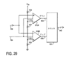
図17は、発明の例示的実施形態に従うボディバイアスコントローラ603のブロック図を示す。ボディバイアスコントローラ603は、基準信号ジェネレータ625、遅延回路612、位相比較器637、およびボディバイアスジェネレータ430を含む。任意に、ボディバイアスコントローラ603は、詳細は以下に記述のとおり、MUX627を含み得る。
FIG. 17 shows a block diagram of a
基準信号ジェネレータ625は、クロック信号628から基準信号631を生成する。回路の実際の設計およびインプリメンテーションに依存する要因(たとえば、遅延回路612における遅延とユーザー回路609における遅延との関係など)により、基準信号631は、必要に応じ、クロック信号628と特定の関係を有し得る。たとえば、基準信号631は、クロック信号628の半分の周波数を有し得る。基準信号631は、遅延回路612に入力(feed)する。応答して遅延回路612は、基準信号631の遅延バージョンである出力信号634を生成する。
The
必要に応じ、多数のクロック信号628Aの一つを選択する能力を提供するMUX627を任意に使用し得ることに注意されたい。以下に詳細に記述されているように、ボディバイアスコントローラ603は、クロック信号628の周期を使用し基準回路の遅延を測定し、その測定の結果を使用して、ボディバイアス信号を生成しPLD103内の種々の回路へ供給する。MUX627の選択信号627Aによって、選ばれたクロック信号が所望または特定の周期を有するようにクロック信号628Aの一つを選択し得る。その方法によって、ボディバイアスコントローラ603の柔軟性を増加し得る。
Note that
位相比較器637は、基準信号631と遅延回路612の出力信号634を比較する。二つの信号の相対位相によって、比較器637は、出力信号640(スピードアップ)および出力信号643(スローダウン)を生成する。出力信号640および643は、ボディバイアスジェネレータ430を駆動する。ボディバイアスジェネレータ430は、出力信号640および643に応答して、ボディバイアス信号を生成する。図17に示す特定の例において、ボディバイアスジェネレータは、ボディバイアス信号646(νb1)およびボディバイアス信号649(νb2)を生成する。
The
図18は、本発明の例示的実施形態に従う基準信号ジェネレータ625の回路配置を示す。基準信号ジェネレータ625は、フリップフロップ660ならびにインバータ663および666を含む。この特定の例において、基準信号ジェネレータ625は、2で割る回路を構成する。このように、フリップフロップ660およびインバータ663は、クロック信号628の周波数の半分を有する信号を生成する。インバータ666は、その信号をバッファリングし、基準信号631を供給する。本発明の記述からメリットを享受する当業者は理解するように、回路構成およびアプリケーションによって、必要に応じ、インバータ666を使用する必要がなく、それを省き得る。
FIG. 18 shows a circuit arrangement of a
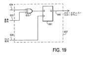
図19は、発明の例示的実施形態に従う位相比較器637の回路配置を示す。比較器637は、排他的OR(XOR)ゲート675、およびフリップフロップ681を含む。遅延回路612の出力は、XORゲート675の1入力に入力(feed)する。基準信号631は、XORゲート675の第2の入力に入力する。
FIG. 19 shows a circuit arrangement of a
XORゲート675の出力は、フリップフロップ681のデータ(D)入力に入力する。クロック信号628はフリップフロップ681および684を駆動する。フリップフロップ681の出力Qは出力信号640
The output of the
![]()
![]()
遅延回路612による遅延がクロック信号628の周期より短い場合、ユーザー回路は、あまりに速く動作する。この場合、ゲート675の出力は、クロック信号628の立ち上がり遷移時にロジックゼロとなる。逆に、遅延回路612による遅延がクロック信号628の周期より長い場合、ユーザー回路は、あまりに遅く動作する。それらの状況の下に、XORゲート675は、クロック信号628の立ち上がり遷移時の出力時にロジックハイ信号を供給する。その結果、フリップフロップ681はスピードアップ出力信号を提供する。
If the delay due to the
図20は、発明の例示的実施形態に従う位相比較器637の別の回路配置を示す。図19と同様に、図20の比較器637は、排他的OR(XOR)ゲート675、排他的NOR(XNOR)ゲート678、およびフリップフロップ681および684を含む。さらに、図20の比較器637は不感帯遅延回路690を含む。不感帯遅延回路690は、PLD103内のトランジスタをより安定に電力効率的なボディバイアス調整を行う。
FIG. 20 shows another circuit arrangement for
より具体的には、不感帯遅延回路690は、XNORゲート678が基準信号634自体よりはむしろ、基準信号634の遅延バージョンを受信する原因となる。不感帯遅延回路690がない場合、比較器637は、ユーザー回路609用の平衡速度、リーク、消費電力を見つけるよう求めるので、比較器のスピードアップおよびスローダウン出力信号を繰り返しおよび交互にアサートし得る。ボディ調整を繰り返す(トランジスタボディの充電と放電)と、電力消費の増加、および従って、効率の低下の原因となる。
More specifically,
不感帯遅延回路690は、比較器637が、その出力時に、「チャタ(chatter)」がより少なくなるように助ける。別の言い方をすると、遅延回路612および不感帯遅延回路690を含む比較器637の場合(すなわち、図20)、一つの遅延回路は最小遅延を形成し、両方の合計は最大の遅延を形成する。クロック信号628の周期が両方の遅延の合計を超えた場合、ユーザー回路609はあまりに速く動作する。その結果、比較器637はスローダウン出力信号をアサートする。
逆に、クロック周期が遅延回路612の遅延より短い場合、ユーザー回路609は、あまりに遅く動作する。その結果、比較器637はスピードアップ出力信号をアサートする。ユーザー回路609が、速度の許容可能または所定の範囲内で(対応するリークおよび消費電力レベルを伴って)動作する場合、比較器637は、その出力信号のいずれもアサートしない。その結果、比較器637は、ユーザー回路609の許容可能な動作速度を達成するために、比較器の出力信号の繰り返しの変更を避ける。
Conversely, when the clock period is shorter than the delay of the
遅延回路612は、固定または調整可能または構成可能な遅延のいずれかを提供し得ることに注意されたい。固定遅延の場合、遅延回路612は、所望または所定の遅延を有するロジック回路を含む。たとえば、遅延回路612は、ゲートなどの組み合わせの論理要素の配置を含み得る。プログラマブルロジック106およびプログラマブルルーティングまたは相互接続109などの、PLD103のプログラマブルリソースを使用して遅延回路612をインプリメントし得る(図1を参照されたい)。
Note that the
代わりに、遅延回路612は、構成可能な遅延を有し得る。図21は、発明に従う例示的実施形態における使用のための構成可能な遅延回路612を示す。図21の遅延回路612は、構成または調整信号703の1セットを受け入れる。信号703は、B0〜Biで示されるビットの1セットを含む。構成信号703は、遅延回路612の遅延を調整または構成する。換言すると、構成信号703においてビットの値を設定することによって、時間量を調整し得、その時間量によって遅延回路612は、その出力信号を生成するためにその入力信号を遅延させる。
Instead, the
図22は、発明の例示的実施形態に従う構成可能な遅延回路の回路配置を示す。構成可能な遅延回路は、相互接続またはルーティング遅延要素710の1セットのカスケード結合、ロジック遅延要素719の1セットのカスケード結合、MUX713およびMUX725を含む。
FIG. 22 shows a circuit arrangement of a configurable delay circuit according to an exemplary embodiment of the invention. Configurable delay circuits include a set of cascaded connections of interconnect or routing
ルーティング遅延要素710の出力信号は、MUX713の入力信号を構成する。MUX713はまた、一つ以上の選択信号716を受信する。本発明の記述からメリットを享受する当業者は理解するように、選択信号716の数は、ルーティング遅延要素710の数に依存する。選択信号716によって、ルーティング遅延要素710の一つの出力をMUX713の出力に選択的に結合し得る。このように、第1のルーティング遅延要素の入力信号(基準信号631)からMUX713の出力までの遅延の量を構成し得る。
The output signal of the
同様に、ロジック遅延要素719の出力信号は、MUX725の入力信号を供給。MUX725もまた、一つ以上の選択信号728を受信する。本発明の記述からメリットを享受する当業者は理解するように、選択信号728の数は、ロジック遅延要素719に依存する。選択信号728を使用することによって、ロジック遅延要素719の一つの出力をMUX728の出力へ選択的に結合し得る。従って、第1のロジック遅延要素の入力信号(すなわち、MUX713の出力信号)からMUX725の出力までの遅延の量を構成し得る。
Similarly, the output signal of
MUX713およびMUX725を使用することによって、所望数のルーティング遅延要素710とロジック遅延要素719とのそれぞれの遅延組み合わせを構成するために構成可能な遅延回路の遅延を構成し得る。このように、遅延回路の遅延がユーザーの回路の遅延を表すように、遅延回路を構成し得る(たとえば、詳細上記のPLD構成ソフトウェアによって)。さらに、必要に応じ、ダイナミックな方法で(変化する動作環境、外部制御、ユーザー制御に応答して)遅延を構成し得る。
By using
図23は、本発明の例示的実施形態に従うルーティング遅延要素710用の回路配置を示す。ルーティング遅延要素710は、MUX735およびインバータ738を含む。MUX735およびインバータ738は、一緒になって、PLD103内の代表的なルーティングメカニズム(その対応する遅延を含む)を表すよう捜す。MUX735は、その入力の一つおよびその選択入力が接地され、その結果、MUX735はその入力信号をインバータ738に結合する。インバータ738の出力信号は、ルーティング遅延要素738の出力信号を構成する。このように、ルーティング遅延ロジック710は、その出力信号としてその入力信号の反転したバージョンを供給する。
FIG. 23 shows a circuit arrangement for a
図24は、発明の例示的実施形態に従うロジック遅延要素719の回路配置を示す。ロジック遅延要素719は、送信ゲート745、送信ゲート748、インバータ751、およびインバータ754を含む。ロジック遅延要素719内の回路要素は、一緒になって、PLD103内のプログラマブルロジック回路(およびその回路の対応する遅延)を表すように求める。送信ゲート745および748およびインバータ751は、入力信号(そのロジック値に関わらず)をインバータ754の入力に結合するためのメカニズムを提供する。インバータ754の出力信号は、ロジック遅延要素719の出力信号を構成する。このように、ロジック遅延ロジック719は、その出力信号としてその入力信号の反転したバージョンを供給する。
FIG. 24 shows a circuit arrangement of a
図(たとえば、図18〜20および22〜24)は、図が表すそれぞれの回路の例示的な実施形態を提供するに過ぎないことに注意されたい。本発明の記述からメリットを享受する当業者は理解するように、設計および性能仕様などの要因によって、必要に応じ、その他の回路および実施形態を使用し得る。 Note that the figures (eg, FIGS. 18-20 and 22-24) only provide exemplary embodiments of the respective circuits that the figures represent. Those skilled in the art who have the benefit of the description of the invention will appreciate that other circuits and embodiments may be used as needed, depending on factors such as design and performance specifications.
単なる一例として、離散的時間出力値を有する比較器を使用するよりはむしろ、連続的時間出力値を有する比較器を使用し得る。さらに、調整可能またはプログラマブルなボディバイアス信号をPLD103の種々のパーツに供給するために、必要に応じ、二つ以上のボディバイアスコントローラ603(および比較器)を使用し得る。
By way of example only, rather than using a comparator with discrete time output values, a comparator with continuous time output values may be used. In addition, two or more body bias controllers 603 (and comparators) may be used as needed to provide adjustable or programmable body bias signals to the various parts of the
別の例として、必要に応じ、たとえば、制御回路網136(図1を参照されたい)のパーツとしての専用の回路網を使用して、図にある種々の回路(たとえば、ボディバイアスコントローラ603)を実現し得る。代案として、必要に応じ、PLD103のプログラマブルリソースにおけるそれらの回路(たとえば、図1、図3、および図4を参照されたい)すなわち、プログラマブルロジック106およびプログラマブル相互接続109、をインプリメントし得る。本発明の記述からメリットを享受する当業者は、これらの二つの手法の組み合わせを使用し得ること理解する。換言すると、必要に応じ、一部ではPLD103のプログラマブルリソースを使用することによって、および、一部では専用の回路網を使用して、回路網を実現し得る。インプリメンテーションがPLDプログラマブルリソースを使用する場合、PLD CADソフトウェアは(たとえば、図6Aおよび附属の説明を参照されたい)、PLD103のプログラマブル構造(プログラマブルロジック106およびプログラマブル相互接続109)内の種々の回路要素を配置し、伝送する。
As another example, various circuits (eg, body bias controller 603) shown in the figure may be used as needed, eg, using dedicated circuitry as part of control circuitry 136 (see FIG. 1). Can be realized. Alternatively, those circuits in the programmable resources of PLD 103 (see, eg, FIGS. 1, 3, and 4), ie,
さらに、PLD CADソフトウェアは、遅延回路112をインプリメントする回路要素(組み合わせのロジック要素またはルーティング遅延要素710およびロジック遅延要素719)を選択、配置、および伝送する。PLD CADソフトウェアは、遅延回路612がユーザー回路609の遅延を表すように回路要素を選択する。PLD CADソフトウェアは、構成メモリ133のビット値をプログラムし(図1を参照されたい)、構成メモリ133は、その後、MUX選択信号627A(図17を参照されたい)および構成信号703(図21を参照されたい)などの種々の構成またはプログラム信号用の値を供給する。代わりの実施形態において、ユーザーは、ユーザー回路609をモデルにするため、遅延回路612のパラメータを定義し得る。代わりの実施形態は、ユーザーに対しPLD回路網の性能をユーザーの仕様または要件に適合させる能力を提供する。
In addition, the PLD CAD software selects, places, and transmits circuit elements (combined logic elements or routing
一つの遅延回路612および比較器637を使用するよりはむしろ、その代わりに必要に応じ、複数の遅延回路612および/または比較器637を使用し得ることに注意されたい。そうすることによって、遅延連鎖によって提供される遅延のより多くの解決、および従って、ボディバイアスコントローラの収束の改善を提供し得る。
Note that rather than using a
開示の別の局面は、一般に、IC内のトランジスタの性能(リーク、速度、およびワット損)を直接に調整またはプログラムする(それらのトランジスタを含む回路の性能をモデルにする遅延回路を使用するよりはむしろ)ことに関する。より具体的には、IC内の一つ以上のトランジスタのリークレベルをトランジスタのボディバイアスをプログラムまたは調整することによって設定するために、リークロックループ(LLL)を使用し得る。 Another aspect of the disclosure is generally directly adjusting or programming the performance (leakage, speed, and power dissipation) of the transistors in the IC (rather than using a delay circuit that models the performance of the circuit containing those transistors). Rather)). More specifically, a leaky clock loop (LLL) may be used to set the leakage level of one or more transistors in an IC by programming or adjusting the body bias of the transistors.
リークロックループ技術は、リーク電流の尺度としての代表遅延を使用することによる間接制御よりはむしろ、その技術が回路のリークを直接に制御する能力を提供するというメリット有する。その技術は、ユーザーが許容または所望リークレベルを指定し、性能とリーク電流およびワット損との間の所望のトレードオフを選択し指定することを可能にする。リークロックループのコンセプトを、一般に、PLDを含むICに適用し得ることに注意されたい。 Rie clock loop technology has the advantage that it provides the ability to directly control circuit leakage rather than indirect control by using a representative delay as a measure of leakage current. The technique allows a user to specify an acceptable or desired leak level and select and specify a desired trade-off between performance and leakage current and power dissipation. Note that the concept of leaky clock loops can generally be applied to ICs including PLDs.
図25は、発明の例示的実施形態に従った、リークロックループのブロック図を示す。リークロックループは、基準トランジスタ760、リーク測定回路766、加算器775、およびボディバイアスジェネレータ430を含む。一般的に言って、リークロックループは負フィードバック回路を含む。リークロックループは、IC回路763内のトランジスタのリーク電流を測定するために、基準トランジスタ760を使用し、それらのトランジスタ用のボディバイアス信号を生成するために、測定されたリーク電流を使用する。
FIG. 25 shows a block diagram of a leaky clock loop according to an exemplary embodiment of the invention. The leaky clock loop includes a
必要に応じ、また、本発明の記述からメリットを享受する当業者は理解するように、他の量を測定するリークロックループの他の実施形態を設計し得、一つ以上のユーザー指定の基準を満たすように一つ以上のトランジスタのボディバイアスを調整し得ることに注意されたい。そのような量の例は、基準トランジスタの閾値電圧(VT)または基準トランジスタの飽和電流(Idsat)を含む。 If desired, and as those skilled in the art who have the benefit of the description of the invention will appreciate, other embodiments of leaky clock loops that measure other quantities can be designed to provide one or more user-specified criteria. Note that the body bias of one or more transistors can be adjusted to satisfy. Examples of such quantities include reference transistor threshold voltage (V T ) or reference transistor saturation current (I dsat ).
基準トランジスタ760は、IC回路763にある。必要に応じ、二つ以上の基準トランジスタ760を使用し得ること(たとえば、IC回路763の二箇所以上の場所におけるリーク電流を測定すること)に注意されたい。IC回路763は、ICの性能がボディバイアスレベルによって調整またはプログラムされるように求められるそのIC内の回路網を構成する。たとえば、ICはPLDであるという状況において、IC回路763は、ユーザー回路609を構成し得る(たとえば、図16を参照されたい)。
The
一般に、IC回路763のトランジスタ(基準トランジスタ760を含む)が同様な電気的特性を有するようにし、条件の変動(たとえば、処理、電圧、および温度、またはPVT)がIC回路763全体のボディバイアスのプログラムを実質的に劣化しないように、IC内の回路網の十分に小さな部分を含めて、IC回路763を選択する。
In general, the transistors of IC circuit 763 (including reference transistor 760) have similar electrical characteristics, and variations in conditions (eg, process, voltage, and temperature, or PVT) are subject to body bias across
リーク測定回路766は、基準トランジスタ760のリークを測定し、リーク信号769を加算器775へ供給する。加算器775は、リーク信号769を基準リーク信号(νref)772に比較し、エラー信号778を生成する。ボディバイアスジェネレータ430は、エラー信号を使用し、一つ以上のボディバイアス信号435を生成する。ボディバイアスジェネレータ430は、ボディバイアス信号435をIC回路760内の所望のトランジスタに供給する。
The
図25のリークロックループにおいて、必要に応じ、構成可能コンポーネントを使用し得ることに注意されたい。たとえば、必要に応じ、リーク測定回路766(構成可能利得)、構成可能加算器775(構成可能利得)または加算器775に続く個別の利得ブロック、構成可能基準リーク信号772(構成可能レベル)、および/またはボディバイアスジェネレータ430における構成可能利得を使用し得る。PLD構成RAMビット、PLD上のユーザー回路からの信号、またはこの二つの組み合わせを、それらの構成可能コンポーネントの各々を構成するために、必要に応じ、使用し得ることに注意されたい。
Note that configurable components may be used as needed in the leaky clock loop of FIG. For example, if desired, a leak measurement circuit 766 (configurable gain), a configurable adder 775 (configurable gain) or a separate gain block following the
図26は、発明の別の例示的実施形態に従ったリークロックループのブロック図を示す。図26におけるリークロックループは、基準トランジスタ760(IC回路763にある)、リーク測定回路766、基準値および比較器回路775、フィルタ787、およびボディバイアスジェネレータ430を含む。
FIG. 26 shows a block diagram of a leaky clock loop according to another exemplary embodiment of the invention. The leaky clock loop in FIG. 26 includes a reference transistor 760 (in IC circuit 763), a
基準トランジスタ760およびIC回路763は、図25に関連する上記のそれらのものと同じかまたは同様の構成を有する。リーク測定回路766は、制御信号781によって、プログラマブル利得を供給する。より具体的には、リーク測定回路766がリーク信号769を供給するために、測定されたリーク電流に印加する利得は、制御信号781によって、調整し得る。
基準値および比較器回路775は、リーク信号を処理する。基準値および比較器回路775は、必要に応じて、プログラマブル基準値、プログラマブル利得、またはその両方を、制御信号784によって供給する。換言すると、制御信号784によって、基準リーク信号(図25の基準リーク信号772に類似した)、リーク信号769を基準リーク信号と比較しリークエラー信号778を生成する比較器(明白には示されていない)、またはその両方を、必要に応じ、調整し得る。基準値および比較器回路775は、必要に応じて、比較器の出力信号を量子化する量子化器を任意に含み得る。
The reference value and
フィルタ787は、リークエラー信号778を濾波および処理し、濾波された信号790を生成する。ボディバイアスジェネレータ430は、図25に関連する上記の方法で動作し、一つ以上のボディバイアス信号をIC回路263に供給する。
必要に応じ、フィルタ787をリークロックループから省略し得ることに注意されたい。フィルタ787は、利得ブロックまたは回路、ローパス転送機能または積分器トランジスタ機能などの所望の転送機能を有し得る。本発明の記述からメリットを享受する当業者は理解するように、フィルタ787およびその特定の転送機能を含めるかどうかの選択は、設計および性能仕様ならびに考慮に依存する。
Note that
必要に応じ、リーク測定回路766、および、基準値および比較器回路775を種々の方法によって実行し得る。本発明の記述からメリットを享受する当業者は理解するように、回路の選択およびインプリメンテーションは、種々の要因(たとえば、使用されるIC技術、所望の性能特性など)に依存する。図27〜図29は、いくつかの例を提供する。
If desired, the
図27は、発明の例示的実施形態に従ったリーク測定回路766を示す。リーク測定回路766は、PMOSトランジスタ803および805、基準トランジスタ760、および複数のNMOSトランジスタ808A〜808Dを含む。
FIG. 27 shows a
基準トランジスタ760のゲートはそのソースに結合し、そのことは、基準トランジスタ760をオフ状態にする。このように、基準トランジスタ760を通じて伝導される電流は、基準トランジスタのリーク電流を表す。トランジスタ803は、基準トランジスタ760とシリアルに結合する。トランジスタ803のゲートは、そのトランジスタのドレインに結合する(いわゆる「ダイオード接続構成」)。
The gate of
トランジスタ803およびトランジスタ805は、電流ミラーを形成する。電流ミラーは、リーク電流(基準トランジスタ760を通った電流)を増幅する。本発明の記述からメリットを享受する当業者は理解するように、増幅のレベルは、トランジスタ803および805の相対サイズに依存する。
電流ミラーによって増幅される電流は、オン状態の任意のトランジスタ808A〜808Dを通して流れる。トランジスタ808A〜808Dは、構成可能な出力電流(リーク電流769)を供給する。適切なレベルの制御信号781を印加することによってトランジスタ808A〜808Dを選択的にオンにすることによって、出力電流を構成し得る。一般に、iビットを有する制御信号781に関して、基準電流の2iレベルを供給する。トランジスタ808A〜808Dは、制御信号781に応答し所望の基準電流プロファイルを供給するように選択された相対サイズを有し得る。
The current amplified by the current mirror flows through any
本発明の記述からメリットを享受する当業者は理解するように、トランジスタの数とサイズの種々の組み合わせを使用し得る。一例として、トランジスタ808B〜808Dの各々がその前のトランジスタの2倍の幅を有するように(2進重み付け構成)、トランジスタ808A〜808Dのサイズを決め得る。一つの例示的実施形態において、所定のチャネル長に関して、トランジスタ760は200の幅を有し、トランジスタ803は1の幅、トランジスタ805は50の幅、トランジスタ808Aは1の幅、およびトランジスタ808B〜808Dは2進重み付け幅を有する(すなわち、トランジスタ808Bは2の幅、トランジスタ808Cは4の幅、など)。
As those skilled in the art who have the benefit of the description of the invention understand, various combinations of transistor numbers and sizes may be used. As an example,
図28は、発明の例示的実施形態に従った基準値および比較器回路775を示す。回路は、抵抗818、抵抗821および比較器815を含む。抵抗818および821は、リーク基準信号772を比較器815に供給する分圧器を形成する。所望の基準レベルを供給するように、抵抗818および821の値を選択し得る。比較器815は、リーク信号769をリーク基準信号772と比較し、リークエラー信号778を供給する。比較器815は、必要に応じ、構成可能な利得を有し得る(制御信号784に応答して)。図28は簡略な比較器815を示し、その比較器815は、必要に応じ、比較的正確な基準電圧を供給するために安定した基準回路を含め得ることに注意されたい。
FIG. 28 illustrates a reference value and
図29は、発明の別の例示的実施形態に従った基準値および比較器回路775を示す。回路は、抵抗824、抵抗827、抵抗830、比較器815A、比較器815B、およびカウンタ839を含む。比較器815Aおよび/または815Bは、必要に応じ、構成可能な利得を有し得る(制御信号784に応答して)。
FIG. 29 shows a reference value and
図29における基準値および比較器回路775は図28の回路と同様であるが、この回路は、リーク電流用に下限と上限を供給するように二つの基準信号を使用する。より具体的には、抵抗824、827、および830は、リーク基準信号772Aを比較器815Aに供給し、リーク基準信号772Bを比較器815Bに供給する分圧器を形成する。リーク基準信号772Aおよび772Bは、リーク電流用の上下限を構成する。別の言い方をすると、リーク基準信号772Aおよび772Bは、リーク電流用の値の「ウィンドウ」を供給する。リーク基準信号772Aおよび772Bの所望のレベルを供給するように、抵抗824、827、および830の値を選択し得る。
The reference value and
比較器815Aは、リーク信号769をリーク基準信号772Aと比較し、ダウン信号833を供給する。ダウン信号833は、カウンタ839をカウントダウンさせる(すなわち、IC回路の動作速度を下げる)。逆に、比較器815Bは、リーク信号769をリーク基準信号772Bと比較し、アップ信号836を供給する。アップ信号836は、カウンタ839をカウントアップさせる(すなわち、IC回路の動作速度を上げる)。別の言い方をすると、カウンタ839は、図26のフィルタ787としての積分器を使用することに類似している。カウント信号842は、カウンタ839の電流カウント値を提供する。ボディバイアスジェネレータ430(図29に示されない)カウント信号842を使用し、ボディバイアス信号435(図29に示されない)を生成し、その信号をIC回路763に供給する。
ボディバイアスレベルの制御またはプログラムをさらに供給するために、必要に応じ、IC内に二つ以上のボディバイアスジェネレータ回路430を含め得る。そのような構成において、各ボディバイアスジェネレータ430は一つ以上のボディバイアス信号435を回路(IC回路763など)またはIC内の領域に供給する。
More than one body
このように、ボディバイアスジェネレータ430をプログラムし、ICの各回路または領域用の特定のまたは個々に区別されたボディバイアス信号を供給し得る。代案として、ユーザーは、ICの所定の回路または領域用にボディバイアス信号435の所望の数およびレベルを生成するようにボディバイアスジェネレータ430用のプログラムを特定し、または供給し得る。特に適合されまたはプログラムされたボディバイアスレベルは、ICの各回路または領域用に性能とリークおよびワット損とのトレードオフを可能にする。その結果、ユーザーは、より細かい粒状度で、IC内の種々の部品および回路について性能と電力とのトレードオフに対する制御を増加させる。
In this manner,
図30は、発明の例示的実施形態に従った、ICにおける複数のボディバイアス回路を供給するための回路配置を示す。回路配置は、IC領域870、IC回路763A〜763Cのセット、対応する数のMUX875A〜875C、およびボディバイアスジェネレータ435A〜435Cを含む。
FIG. 30 shows a circuit arrangement for providing a plurality of body bias circuits in an IC according to an exemplary embodiment of the invention. The circuit arrangement includes an
ボディバイアスジェネレータ430A〜430Cの各々は、ボディバイアス信号435A〜435Cとして示される一つ以上のボディバイアス信号を生成し、信号をMUX875A〜875Cの各々に供給する。選択信号880に応答し、MUX875A〜875Cの各々は、ボディバイアスジェネレータ435A〜435Cの一つからのボディバイアス信号を選択し、選択されたボディバイアス信号をIC回路763A〜763Cの対応する一つに供給する。
Each of
MUX875A〜875Cを使用するよりはむしろ、プログラマブル不揮発性結合メカニズム(ヒューズなど)を使用し得る。そのような状況において、個々のICの特性(たとえば、リークのレベル)を判定するために、製作後個々のICをテストし得、所望または適切なボディバイアス信号をICの種々の領域または回路に供給するように不揮発性結合メカニズムをプログラムし得る。多数のボディバイアスジェネレータを含むことによって、ユーザーは、それらの領域または回路のボディバイアスレベルを独立してプログラムする能力が与えられる。
Rather than using
別の実施形態において、不揮発性メモリに記憶された値(ICの特性(たとえば、リークレベル)またはIC内の特定の領域または回路に関係する値など)とユーザー構成またはユーザー特定の値との組み合わせを使用し、ボディバイアスレベルを生成し得る。この案は、性能とワット損およびリークレベルとをトレードオフするために、ICの特性およびユーザー特定のパラメータの両方を考慮に入れることを可能にする。 In another embodiment, a combination of a value stored in non-volatile memory (such as a characteristic of an IC (eg, a leak level) or a value related to a particular region or circuit within the IC) and a user configuration or user-specific value Can be used to generate a body bias level. This scheme makes it possible to take into account both IC characteristics and user-specific parameters in order to trade off performance for power dissipation and leakage levels.
PLDの場合、PLD領域870は、PLD領域606を構成し得(たとえば、図25を参照されたい)、各IC回路763はユーザー回路609に対応し得る。一つ以上の適合またはプログラムされたボディバイアス信号435をPLD103内の各ユーザー回路609(たとえば、図25を参照されたい)に供給し得る。別の実施形態において、IC回路763は、PLD回路(プログラマブルロジック106およびプログラマブル相互接続109)の物理的に近いセット、またはプログラマブルロジック106およびプログラマブル相互接続109の選択されたグループ(たとえば、図3の長方形のアレイに配列されたプログラマブルロジック回路106のグループ)に対応し得る。
In the case of a PLD, the
図30は、ボディバイアス信号435A〜435Cを供給する回路網としてのボディバイアスジェネレータ430A〜430Cを示す。PLDの場合、一般に、ボディバイアスジェネレータ430A〜430Cよりはむしろ、ボディバイアスコントローラ603A〜603C(たとえば、図25を参照されたい)を使用し得る。
FIG. 30 shows
図30は、IC回路763A〜763Cを含むとしてのIC領域870を示すことに注意されたい。しかし、本発明の記述からメリットを享受する当業者は理解するように、逆の状況が存在し得る(すなわち、各IC回路は一つ以上のIC領域870含み得る)。
Note that FIG. 30
上記の性能同調コンセプトをその他の技術と組み合わせ、出力密度を減少し、または出力密度を安全な範囲内に維持し得ることにさらに注意されたい。たとえば、PLD内の種々の回路をオンまたはオフにし得(図9および添付の説明を参照されたい)、所望の性能レベルと安全または所定の消費電力レベルまたは出力密度とのトレードオフを達成し得る。その他の変種および実施形態は、本発明の記述からメリットを享受する当業者にとって、明らかであろう。 It should be further noted that the performance tuning concept described above can be combined with other technologies to reduce power density or keep power density within a safe range. For example, various circuits in the PLD can be turned on or off (see FIG. 9 and accompanying description) to achieve a trade-off between a desired performance level and a safe or predetermined power consumption level or power density. . Other variations and embodiments will be apparent to those skilled in the art from the description of the invention.
一般に、必要に応じ、また、本発明の記述からメリットを享受する当業者は理解するように、発明コンセプトを、当業界で他の名前で公知の種々のプログラマブルロジック回路網またはICへ効果的に適用し得ることに注意されたい。そのような回路網は、複合プログラマブルロジックデバイス(CPLD)、プログラマブルゲートアレイ(PGA)、およびフィールドプログラマブルゲートアレイ(FPGA)として公知のデバイスを含む。 In general, the inventive concept can be effectively applied to various programmable logic networks or ICs known elsewhere in the art as needed and as will be appreciated by those skilled in the art who will benefit from the description of the invention. Note that it may apply. Such circuitry includes devices known as complex programmable logic devices (CPLD), programmable gate arrays (PGA), and field programmable gate arrays (FPGA).
図を参照すると、当業者は、示された種々のブロックは主としてコンセプトの機能および信号流れを示し得ることに気づく。実際の回路インプリメンテーションは、種々の機能ブロック用の別々に識別可能なハードウェアを含み得または含まれ得なく、また、示された特定の回路網を使用し得または使用し得ない。 Referring to the figure, those skilled in the art will notice that the various blocks shown may primarily represent the function and signal flow of the concept. The actual circuit implementation may or may not include separately identifiable hardware for the various functional blocks, and may or may not use the particular circuitry shown.
たとえば、必要に応じ、種々のブロックの機能性を一つの回路ブロックに結合し得る。さらに、必要に応じ、いくつかの回路ブロックにおいて一つのブロックの機能性を実現し得る。本発明の記述からメリットを享受する当業者は理解するように、回路インプリメンテーションの選択は、所定のインプリメンテーション用の特定の設計および性能仕様などの種々の要因に依存する。 For example, the functionality of various blocks can be combined into a single circuit block as needed. Furthermore, the functionality of one block can be realized in several circuit blocks as required. As those skilled in the art who have the benefit of the description of the invention will appreciate, the choice of circuit implementation depends on various factors such as the specific design and performance specifications for a given implementation.
この明細書に記述された発明の実施形態に加えて、その他の修正および代わりの実施形態は、本発明の記述からメリットを享受する当業者にとって、明らかであろう。従って、この記述は、当業者に発明の実施方法を教え、例示的としてのみと解釈すべきである。 In addition to the embodiments of the invention described in this specification, other modifications and alternative embodiments will be apparent to those skilled in the art who have the benefit of the description of the invention. Accordingly, this description teaches those skilled in the art how to practice the invention and should be construed as illustrative only.
示され記述された発明の形式は、現在好適なまたは例示的な実施形態として解すべきである。当業者は、本明細書に記述された発明の範囲から逸脱することなく、形状、サイズ、および部品の配置における種々の変更を行い得る。たとえば、当業者は、本明細書に例示および記述されたエレメントの代わりに同等のエレメントを用い得る。さらに、本発明の記述からメリットを享受する当業者は、発明の範囲から逸脱することなく、発明の特定の特徴を他の特徴の使用とは無関係に使用し得る。 The form of the invention shown and described is to be understood as a presently preferred or exemplary embodiment. Those skilled in the art may make various changes in shape, size, and arrangement of parts without departing from the scope of the invention described herein. For example, those skilled in the art may substitute equivalent elements for the elements illustrated and described herein. Moreover, those skilled in the art who have the benefit of the description of the invention may use certain features of the invention independently of the use of other features without departing from the scope of the invention.
Claims (64)
遅延回路であって、該プログラマブルロジックデバイス(PLD)においてインプリメントされるユーザー回路の遅延を表すように構成された遅延を有する遅延回路と、
ボディバイアスジェネレータであって、該遅延回路の伝播遅延から引き出されたレベルに応答する該ユーザー回路内のトランジスタのボディバイアスを調整するように構成されたボディバイアスジェネレータと
を備える、プログラマブルロジックデバイス(PLD)。 A programmable logic device (PLD),
A delay circuit having a delay configured to represent a delay of a user circuit implemented in the programmable logic device (PLD);
A body bias generator comprising: a body bias generator configured to adjust a body bias of a transistor in the user circuit responsive to a level derived from a propagation delay of the delay circuit; ).
該プログラマブルロジックデバイス(PLD)においてインプリメントされるユーザー回路の伝播遅延を表す遅延を生成するための手段と、
該生成された遅延に従って少なくとも一つの信号を引き出すための手段と、
該少なくとも一つの信号に応答して該ユーザー回路にあるトランジスタのボディバイアスをプログラムするための手段と
を備える、プログラマブルロジックデバイス(PLD)。 A programmable logic device (PLD),
Means for generating a delay representative of a propagation delay of a user circuit implemented in the programmable logic device (PLD);
Means for extracting at least one signal in accordance with the generated delay;
Means for programming a body bias of a transistor in the user circuit in response to the at least one signal.
基準トランジスタであって、該プログラマブルロジックデバイス(PLD)における回路に関係した電流を供給するように構成された該基準トランジスタと、
電流測定回路であって、該基準トランジスタによって供給された該電流を測定し、測定された電流信号を供給するように構成された該測定回路と、
ボディバイアスジェネレータであって、該測定された電流信号からの少なくとも一つのボディバイアス信号を引き出すように構成され、該ボディバイアスジェネレータは、該少なくとも一つのボディバイアス信号を該プログラマブルロジックデバイス(PLD)における回路に供給するようにさらに構成される該ボディバイアスジェネレータと
を備える、プログラマブルロジックデバイス(PLD)。 A programmable logic device (PLD),
A reference transistor, the reference transistor configured to supply a current related to a circuit in the programmable logic device (PLD);
A current measurement circuit configured to measure the current supplied by the reference transistor and to provide a measured current signal;
A body bias generator configured to derive at least one body bias signal from the measured current signal, the body bias generator generating the at least one body bias signal in the programmable logic device (PLD); A programmable logic device (PLD) comprising: the body bias generator further configured to supply a circuit.
をさらに備える、請求項19に記載のプログラマブルロジックデバイス(PLD)。 A comparator coupled to the current measurement circuit and the body bias generator, wherein the comparator is configured to derive a signal by comparing the measured current signal with a reference signal, the comparator The programmable logic device (PLD) of claim 19, further comprising a comparator further configured to provide the signal to the body bias generator.
をさらに備える、請求項19に記載のプログラマブルロジックデバイス(PLD)。 First and second comparators coupled to the current measurement circuit and the body bias generator, wherein the first and second comparators provide the measured current signals to the first and second comparators. A first pair of signals is derived by comparing with a second reference signal, and the first and second comparators are further configured to supply the pair of signals to the body bias generator. The programmable logic device (PLD) of claim 19, further comprising: a first and a second comparator.
をさらに備える、請求項27に記載のプログラマブルロジックデバイス(PLD)。 A counter coupled to the first and second comparators, the counter configured to count in response to a pair of signals provided by the first and second comparators; 28. The programmable logic device (PLD) of claim 27, wherein the counter further comprises a counter further configured to provide a count value to the body bias generator.
回路におけるリーク電流を得る手段と、
該リーク電流を測定することによって、測定されたリーク電流を生成する手段と、
該測定されたリーク電流に応答して該回路におけるトランジスタのボディバイアスをプログラムするための手段と
を備える、プログラマブルロジックデバイス(PLD)。 A programmable logic device (PLD),
Means for obtaining a leakage current in the circuit;
Means for generating a measured leakage current by measuring the leakage current;
Means for programming a body bias of a transistor in the circuit in response to the measured leakage current.
複数のボディバイアスジェネレータであって、該複数のボディバイアスジェネレータにおける少なくとも一つのボディバイアスジェネレータは、該複数のユーザー回路における少なくとも一つのユーザー回路内のトランジスタのボディバイアスを選択的に調整するように構成されている複数のボディバイアスジェネレータと
を備える、プログラマブルロジックデバイス(PLD)。 A plurality of user circuits, each of the user circuits implemented in a programmable logic device (PLD);
A plurality of body bias generators, wherein at least one body bias generator in the plurality of body bias generators is configured to selectively adjust a body bias of a transistor in at least one user circuit in the plurality of user circuits. A programmable logic device (PLD) comprising a plurality of body bias generators.
設計を生成するために、該電子回路を該プログラマブルロジックデバイス(PLD)内の機能リソースにマッピングするステップと、
該生成された設計の少なくとも一つの部分内の信号伝播遅延を表す遅延からボディバイアス値を引き出すステップと、
該生成された設計の該少なくとも一つの部分内の少なくとも一つのトランジスタのボディバイアスレベルを該ボディバイアス値へプログラムするステップと
を包含する、方法。 A method of using a programmable logic device (PLD) to implement an electronic circuit comprising:
Mapping the electronic circuit to a functional resource in the programmable logic device (PLD) to generate a design;
Deriving a body bias value from a delay representative of a signal propagation delay within at least one portion of the generated design;
Programming the body bias level of at least one transistor in the at least one portion of the generated design to the body bias value.
該トランジスタのリーク電流を表す電流を得るステップと、
該得られた電流からボディバイアスレベルを引き出すステップと、
該トランジスタの該ボディバイアスレベルを該引き出されたボディバイアスレベルへ調整するステップと
を包含する、方法。 A method for adjusting a leakage level of a transistor in a circuit implemented in a programmable logic circuit (PLD), the method comprising:
Obtaining a current representative of the leakage current of the transistor;
Deriving a body bias level from the obtained current;
Adjusting the body bias level of the transistor to the derived body bias level.
前記少なくとも一つのエラー信号を濾過し、濾過された信号を生成するステップと、
該濾過した信号からボディバイアスレベルを引き出すステップと
をさらに包含する、請求項56に記載の方法。 A method of deriving a body bias level from the obtained current,
Filtering the at least one error signal to produce a filtered signal;
57. The method of claim 56, further comprising: extracting a body bias level from the filtered signal.
該回路領域における少なくとも一つのトランジスタ用のボディバイアスレベルを選択するステップと、
プログラマブルロジックデバイス(PLD)内の該回路領域の初期配置を生成するステップと、
既存のボディバイアスレベルおよび配置が所定の性能基準を満たさない場合、該回路領域における該少なくとも一つのトランジスタに印加されるべき該ボディバイアスレベルを少なくとも1回別のレベルに変更するステップと
を包含する、方法。 A method for realizing a user circuit in at least one circuit area in a programmable logic circuit (PLD) comprising:
Selecting a body bias level for at least one transistor in the circuit region;
Generating an initial arrangement of the circuit area in a programmable logic device (PLD);
Changing the body bias level to be applied to the at least one transistor in the circuit region to another level at least once if an existing body bias level and arrangement does not meet a predetermined performance criterion. ,Method.
Applications Claiming Priority (3)
| Application Number | Priority Date | Filing Date | Title |
|---|---|---|---|
| US10/848,953 US7348827B2 (en) | 2004-05-19 | 2004-05-19 | Apparatus and methods for adjusting performance of programmable logic devices |
| US10/865,402 US7129745B2 (en) | 2004-05-19 | 2004-06-10 | Apparatus and methods for adjusting performance of integrated circuits |
| PCT/US2005/017265 WO2005116878A2 (en) | 2004-05-19 | 2005-05-18 | Apparatus and methods for adjusting performance of integrated circuits |
Publications (2)
| Publication Number | Publication Date |
|---|---|
| JP2007538474A true JP2007538474A (en) | 2007-12-27 |
| JP2007538474A5 JP2007538474A5 (en) | 2008-07-03 |
Family
ID=34981317
Family Applications (1)
| Application Number | Title | Priority Date | Filing Date |
|---|---|---|---|
| JP2007527379A Pending JP2007538474A (en) | 2004-05-19 | 2005-05-18 | Apparatus and method for tuning integrated circuit performance |
Country Status (5)
| Country | Link |
|---|---|
| US (3) | US7129745B2 (en) |
| EP (1) | EP1776759B1 (en) |
| JP (1) | JP2007538474A (en) |
| CN (1) | CN102361449B (en) |
| WO (1) | WO2005116878A2 (en) |
Cited By (3)
| Publication number | Priority date | Publication date | Assignee | Title |
|---|---|---|---|---|
| JP2007243178A (en) * | 2006-03-06 | 2007-09-20 | Altera Corp | Adjustable transistor body bias circuit network |
| JP2013046068A (en) * | 2011-08-19 | 2013-03-04 | Altera Corp | Apparatus for improving performance of field programmable gate arrays and associated methods |
| WO2021251206A1 (en) * | 2020-06-09 | 2021-12-16 | 三菱電機株式会社 | Learning device, inference device, and development toolchain for programmable logic device |
Families Citing this family (92)
| Publication number | Priority date | Publication date | Assignee | Title |
|---|---|---|---|---|
| US7180322B1 (en) | 2002-04-16 | 2007-02-20 | Transmeta Corporation | Closed loop feedback control of integrated circuits |
| US7886164B1 (en) | 2002-11-14 | 2011-02-08 | Nvidia Corporation | Processor temperature adjustment system and method |
| US7849332B1 (en) | 2002-11-14 | 2010-12-07 | Nvidia Corporation | Processor voltage adjustment system and method |
| US7882369B1 (en) | 2002-11-14 | 2011-02-01 | Nvidia Corporation | Processor performance adjustment system and method |
| US7205758B1 (en) | 2004-02-02 | 2007-04-17 | Transmeta Corporation | Systems and methods for adjusting threshold voltage |
| US7949864B1 (en) * | 2002-12-31 | 2011-05-24 | Vjekoslav Svilan | Balanced adaptive body bias control |
| US7649402B1 (en) | 2003-12-23 | 2010-01-19 | Tien-Min Chen | Feedback-controlled body-bias voltage source |
| US7816742B1 (en) | 2004-09-30 | 2010-10-19 | Koniaris Kleanthes G | Systems and methods for integrated circuits comprising multiple body biasing domains |
| US7859062B1 (en) | 2004-02-02 | 2010-12-28 | Koniaris Kleanthes G | Systems and methods for integrated circuits comprising multiple body biasing domains |
| FR2868181B1 (en) * | 2004-03-29 | 2006-05-26 | Soisic Sa | METHOD FOR SIMULATING A CIRCUIT AT THE STATIONARY STATE |
| US7400167B2 (en) * | 2005-08-16 | 2008-07-15 | Altera Corporation | Apparatus and methods for optimizing the performance of programmable logic devices |
| US7348827B2 (en) * | 2004-05-19 | 2008-03-25 | Altera Corporation | Apparatus and methods for adjusting performance of programmable logic devices |
| US7112997B1 (en) * | 2004-05-19 | 2006-09-26 | Altera Corporation | Apparatus and methods for multi-gate silicon-on-insulator transistors |
| US7326972B2 (en) * | 2004-06-30 | 2008-02-05 | Intel Corporation | Interconnect structure in integrated circuits |
| US7509504B1 (en) | 2004-09-30 | 2009-03-24 | Transmeta Corporation | Systems and methods for control of integrated circuits comprising body biasing systems |
| EP1820083A1 (en) * | 2004-11-10 | 2007-08-22 | Freescale Semiconductor, Inc. | Apparatus and method for controlling voltage and frequency using multiple reference circuits |
| US7739531B1 (en) | 2005-03-04 | 2010-06-15 | Nvidia Corporation | Dynamic voltage scaling |
| US7394708B1 (en) * | 2005-03-18 | 2008-07-01 | Xilinx, Inc. | Adjustable global tap voltage to improve memory cell yield |
| US7295036B1 (en) * | 2005-11-30 | 2007-11-13 | Altera Corporation | Method and system for reducing static leakage current in programmable logic devices |
| WO2007096913A1 (en) * | 2006-02-24 | 2007-08-30 | Stmicroelectronics S.R.L. | Method for designing a complex integrated electronic circuit architecture |
| US7936184B2 (en) * | 2006-02-24 | 2011-05-03 | Altera Corporation | Apparatus and methods for adjusting performance of programmable logic devices |
| US8010931B1 (en) * | 2006-02-24 | 2011-08-30 | University Of Southern California | Tool for a configurable integrated circuit that uses determination of dynamic power consumption |
| US7330049B2 (en) * | 2006-03-06 | 2008-02-12 | Altera Corporation | Adjustable transistor body bias generation circuitry with latch-up prevention |
| US7355437B2 (en) | 2006-03-06 | 2008-04-08 | Altera Corporation | Latch-up prevention circuitry for integrated circuits with transistor body biasing |
| US7486106B1 (en) * | 2006-03-24 | 2009-02-03 | Altera Corporation | CPLD for multi-wire keyboard decode with timed power control circuit |
| US7463057B1 (en) | 2006-03-29 | 2008-12-09 | Altera Corporation | Integrated circuits with adjustable memory element power supplies |
| US7891865B2 (en) * | 2006-05-03 | 2011-02-22 | International Business Machines Corporation | Structure for bolometric on-chip temperature sensor |
| JP2007311535A (en) * | 2006-05-18 | 2007-11-29 | Matsushita Electric Ind Co Ltd | Cell arrangement method |
| KR100784908B1 (en) * | 2006-08-11 | 2007-12-11 | 주식회사 하이닉스반도체 | Apparatus for trimming voltage |
| US20080180129A1 (en) * | 2006-08-31 | 2008-07-31 | Actel Corporation | Fpga architecture with threshold voltage compensation and reduced leakage |
| US7388531B1 (en) * | 2006-09-26 | 2008-06-17 | Marvell International Ltd. | Current steering DAC using thin oxide devices |
| US7826549B1 (en) * | 2006-11-02 | 2010-11-02 | Sudhir Aggarwal | Wireless communication transmitter and system having the same |
| US8705300B1 (en) * | 2007-02-27 | 2014-04-22 | Altera Corporation | Memory array circuitry with stability enhancement features |
| US7889751B2 (en) * | 2007-03-06 | 2011-02-15 | Sudhir Aggarwal | Low power wireless communication system |
| US9134782B2 (en) | 2007-05-07 | 2015-09-15 | Nvidia Corporation | Maintaining optimum voltage supply to match performance of an integrated circuit |
| JP5162956B2 (en) * | 2007-05-11 | 2013-03-13 | ソニー株式会社 | Semiconductor integrated circuit and operation method thereof |
| US7716615B2 (en) * | 2007-08-31 | 2010-05-11 | International Business Machines Corporation | Redundant critical path circuits to meet performance requirement |
| US7675317B2 (en) * | 2007-09-14 | 2010-03-09 | Altera Corporation | Integrated circuits with adjustable body bias and power supply circuitry |
| US8949763B1 (en) * | 2007-10-02 | 2015-02-03 | Altera Corporation | Apparatus and methods for optimization of integrated circuits |
| US7890893B2 (en) * | 2008-01-10 | 2011-02-15 | International Business Machines Corporation | Design structure for semiconductor on-chip repair scheme for negative bias temperature instability |
| US7679537B2 (en) * | 2008-01-21 | 2010-03-16 | Honeywell International Inc. | Precision microcontroller-based pulse width modulation digital-to-analog conversion circuit and method |
| US8370663B2 (en) | 2008-02-11 | 2013-02-05 | Nvidia Corporation | Power management with dynamic frequency adjustments |
| US20090267588A1 (en) * | 2008-04-23 | 2009-10-29 | Schmitz Michael J | Method and apparatus to dynamically control impedance to maximize power supply |
| US8102187B2 (en) * | 2008-05-02 | 2012-01-24 | Texas Instruments Incorporated | Localized calibration of programmable digital logic cells |
| US20090292849A1 (en) * | 2008-05-22 | 2009-11-26 | Khoo Ken | Adaptable pci express controller core |
| US20090302887A1 (en) * | 2008-06-10 | 2009-12-10 | Tad Kwasniewski | Apparatus for power consumption reduction in programmable logic devices and associated methods |
| US7639041B1 (en) * | 2008-07-28 | 2009-12-29 | Altera Corporation | Hotsocket-compatible body bias circuitry with power-up current reduction capabilities |
| US8099704B1 (en) * | 2008-07-28 | 2012-01-17 | Altera Corporation | Performance improvements in an integrated circuit by selectively applying forward bias voltages |
| US7952423B2 (en) * | 2008-09-30 | 2011-05-31 | Altera Corporation | Process/design methodology to enable high performance logic and analog circuits using a single process |
| WO2010052607A1 (en) * | 2008-11-05 | 2010-05-14 | Nxp B.V. | Body biasing |
| US7911261B1 (en) | 2009-04-13 | 2011-03-22 | Netlogic Microsystems, Inc. | Substrate bias circuit and method for integrated circuit device |
| US8072237B1 (en) | 2009-06-04 | 2011-12-06 | Altera Corporation | Computer-aided design tools and memory element power supply circuitry for selectively overdriving circuit blocks |
| US8181147B2 (en) * | 2009-06-29 | 2012-05-15 | Lsi Corporation | Parametric data-based process monitoring for adaptive body bias control |
| KR101695493B1 (en) | 2009-07-15 | 2017-01-11 | 엘지전자 주식회사 | Cooker and method of controlling the same |
| JP5529450B2 (en) * | 2009-07-15 | 2014-06-25 | スパンション エルエルシー | Body bias control circuit and body bias control method |
| US9256265B2 (en) | 2009-12-30 | 2016-02-09 | Nvidia Corporation | Method and system for artificially and dynamically limiting the framerate of a graphics processing unit |
| US9830889B2 (en) | 2009-12-31 | 2017-11-28 | Nvidia Corporation | Methods and system for artifically and dynamically limiting the display resolution of an application |
| US8839006B2 (en) | 2010-05-28 | 2014-09-16 | Nvidia Corporation | Power consumption reduction systems and methods |
| US8907678B2 (en) * | 2010-12-10 | 2014-12-09 | Raritan Americas, Inc. | Methods and apparatus for sensing ground leakage and automated self testing thereof |
| US9495503B2 (en) * | 2011-04-06 | 2016-11-15 | Qualcomm Incorporated | Method and apparatus to enable a selective push process during manufacturing to improve performance of a selected circuit of an integrated circuit |
| US8816470B2 (en) | 2011-04-21 | 2014-08-26 | International Business Machines Corporation | Independently voltage controlled volume of silicon on a silicon on insulator chip |
| US8456187B2 (en) | 2011-04-21 | 2013-06-04 | International Business Machines Corporation | Implementing temporary disable function of protected circuitry by modulating threshold voltage of timing sensitive circuit |
| US8525245B2 (en) | 2011-04-21 | 2013-09-03 | International Business Machines Corporation | eDRAM having dynamic retention and performance tradeoff |
| US8492207B2 (en) | 2011-04-21 | 2013-07-23 | International Business Machines Corporation | Implementing eFuse circuit with enhanced eFuse blow operation |
| WO2012157532A1 (en) | 2011-05-16 | 2012-11-22 | Semiconductor Energy Laboratory Co., Ltd. | Programmable logic device |
| US8779799B2 (en) | 2011-05-19 | 2014-07-15 | Semiconductor Energy Laboratory Co., Ltd. | Logic circuit |
| JP5892852B2 (en) | 2011-05-20 | 2016-03-23 | 株式会社半導体エネルギー研究所 | Programmable logic device |
| US8669781B2 (en) | 2011-05-31 | 2014-03-11 | Semiconductor Energy Laboratory Co., Ltd. | Semiconductor device |
| KR101318423B1 (en) * | 2011-06-24 | 2013-10-15 | 위니맥스 주식회사 | Water filter assembly and refrigerator and water purifier having the same |
| US8416009B2 (en) | 2011-07-13 | 2013-04-09 | International Business Machines Corporation | Solutions for controlling bulk bias voltage in an extremely thin silicon-on-insulator (ETSOI) integrated circuit chip |
| US8633731B1 (en) | 2011-08-09 | 2014-01-21 | Altera Corporation | Programmable integrated circuit with thin-oxide passgates |
| US8461869B1 (en) * | 2011-08-19 | 2013-06-11 | Altera Corporation | Apparatus for configuring performance of field programmable gate arrays and associated methods |
| US8730713B2 (en) | 2011-09-12 | 2014-05-20 | Qualcomm Incorporated | SRAM cell writability |
| US9436250B1 (en) | 2011-12-19 | 2016-09-06 | Altera Corporation | Apparatus for improving power consumption of communication circuitry and associated methods |
| US8970289B1 (en) | 2012-01-23 | 2015-03-03 | Suvolta, Inc. | Circuits and devices for generating bi-directional body bias voltages, and methods therefor |
| US9201994B1 (en) * | 2013-03-13 | 2015-12-01 | Calypto Design Systems, Inc. | Flexible power query interfaces and infrastructures |
| US9100002B2 (en) * | 2013-09-12 | 2015-08-04 | Micron Technology, Inc. | Apparatus and methods for leakage current reduction in integrated circuits |
| US9444460B1 (en) | 2013-11-22 | 2016-09-13 | Altera Corporation | Integrated circuits with programmable overdrive capabilities |
| US9177096B2 (en) * | 2014-03-26 | 2015-11-03 | Freescale Semiconductor, Inc. | Timing closure using transistor sizing in standard cells |
| KR102140787B1 (en) * | 2014-07-07 | 2020-08-03 | 삼성전자주식회사 | Resistive Memory Device and Operating Method thereof |
| US9628081B2 (en) | 2014-08-12 | 2017-04-18 | Xilinx, Inc. | Interconnect circuits having low threshold voltage P-channel transistors for a programmable integrated circuit |
| US9496871B1 (en) * | 2014-08-18 | 2016-11-15 | Xilinx, Inc. | Programmable power reduction technique using transistor threshold drops |
| US9893725B2 (en) * | 2014-08-27 | 2018-02-13 | Nxp Usa, Inc. | Low side and high side drivers for a motor |
| US9361994B1 (en) * | 2014-09-04 | 2016-06-07 | Cypress Semiconductor Corporation | Method of increasing read current window in non-volatile memory |
| CN105677932A (en) * | 2014-11-19 | 2016-06-15 | 复旦大学 | Statistical timing analysis method used for post-silicon adjustable register circuits |
| US9625924B2 (en) * | 2015-09-22 | 2017-04-18 | Qualcomm Incorporated | Leakage current supply circuit for reducing low drop-out voltage regulator headroom |
| JP2017079037A (en) * | 2015-10-22 | 2017-04-27 | 富士通株式会社 | Arithmetic device and method thereof |
| US9678150B2 (en) * | 2015-10-27 | 2017-06-13 | Xilinx, Inc. | Methods and circuits for debugging circuit designs |
| US9934341B2 (en) | 2015-11-11 | 2018-04-03 | International Business Machines Corporation | Simulation of modifications to microprocessor design |
| US10121534B1 (en) | 2015-12-18 | 2018-11-06 | Altera Corporation | Integrated circuit with overdriven and underdriven pass gates |
| US10591946B2 (en) * | 2017-07-13 | 2020-03-17 | Realtek Semiconductor Corp. | Electronic device, power circuit applied to the electronic device, and associated method |
| IT201900001941A1 (en) * | 2019-02-11 | 2020-08-11 | St Microelectronics Des & Appl | CIRCUIT WITH THE USE OF MOSFETS AND CORRESPONDING PROCEDURE |
Citations (8)
| Publication number | Priority date | Publication date | Assignee | Title |
|---|---|---|---|---|
| JPS61160960A (en) * | 1985-01-08 | 1986-07-21 | Matsushita Electric Ind Co Ltd | Semiconductor ic |
| JPH04247653A (en) * | 1991-02-04 | 1992-09-03 | Ricoh Co Ltd | Delay compensation apparatus of semiconductor integrated circuit device |
| JPH05108194A (en) * | 1991-10-17 | 1993-04-30 | Hitachi Ltd | Low power consumption type semiconductor integrated circuit |
| JP2000101416A (en) * | 1998-09-14 | 2000-04-07 | Texas Instr Inc <Ti> | Pulse operation of body voltage for improving characteristics of mos integrated circuit |
| JP2001156261A (en) * | 1999-09-13 | 2001-06-08 | Hitachi Ltd | Semiconductor integrated-circuit device |
| JP2001345693A (en) * | 2000-05-30 | 2001-12-14 | Hitachi Ltd | Semiconductor integrated circuit device |
| JP2003110028A (en) * | 2001-10-01 | 2003-04-11 | Hitachi Ltd | Data processor |
| JP2003168735A (en) * | 2001-11-30 | 2003-06-13 | Hitachi Ltd | Semiconductor integrated circuit device |
Family Cites Families (63)
| Publication number | Priority date | Publication date | Assignee | Title |
|---|---|---|---|---|
| JPS601071A (en) | 1983-06-18 | 1985-01-07 | 三菱電機株式会社 | Swing bolster device for intermediate truck of electric locomotive |
| JPH0335473A (en) | 1989-06-30 | 1991-02-15 | Mitsubishi Electric Corp | Magnetic recording and reproducing device |
| JPH03269248A (en) | 1990-03-19 | 1991-11-29 | Fujitsu Ltd | Object inspecting apparatus |
| DE4221575C2 (en) * | 1992-07-01 | 1995-02-09 | Ibm | Integrated CMOS semiconductor circuit and data processing system with integrated CMOS semiconductor circuit |
| US5341034A (en) * | 1993-02-11 | 1994-08-23 | Benchmarq Microelectronics, Inc. | Backup battery power controller having channel regions of transistors being biased by power supply or battery |
| KR0169157B1 (en) * | 1993-11-29 | 1999-02-01 | 기다오까 다까시 | Semiconductor circuit and mos-dram |
| US5422591A (en) * | 1994-01-03 | 1995-06-06 | Sgs-Thomson Microelectronics, Inc. | Output driver circuit with body bias control for multiple power supply operation |
| US5689209A (en) * | 1994-12-30 | 1997-11-18 | Siliconix Incorporated | Low-side bidirectional battery disconnect switch |
| JP3641511B2 (en) * | 1995-06-16 | 2005-04-20 | 株式会社ルネサステクノロジ | Semiconductor device |
| US5689144A (en) * | 1996-05-15 | 1997-11-18 | Siliconix Incorporated | Four-terminal power MOSFET switch having reduced threshold voltage and on-resistance |
| US6118302A (en) * | 1996-05-28 | 2000-09-12 | Altera Corporation | Interface for low-voltage semiconductor devices |
| KR100189752B1 (en) * | 1996-06-01 | 1999-06-01 | 구본준 | Power pump circuit with independent well bias voltage |
| JP3264622B2 (en) * | 1996-07-16 | 2002-03-11 | 株式会社東芝 | Semiconductor device |
| US5880620A (en) * | 1997-04-22 | 1999-03-09 | Xilinx, Inc. | Pass gate circuit with body bias control |
| US6593799B2 (en) * | 1997-06-20 | 2003-07-15 | Intel Corporation | Circuit including forward body bias from supply voltage and ground nodes |
| US6411156B1 (en) * | 1997-06-20 | 2002-06-25 | Intel Corporation | Employing transistor body bias in controlling chip parameters |
| US5841694A (en) * | 1997-07-30 | 1998-11-24 | Programmable Silicon Solutions | High performance programmable interconnect |
| US6535034B1 (en) * | 1997-07-30 | 2003-03-18 | Programmable Silicon Solutions | High performance integrated circuit devices adaptable to use lower supply voltages with smaller device geometries |
| US6097242A (en) * | 1998-02-26 | 2000-08-01 | Micron Technology, Inc. | Threshold voltage compensation circuits for low voltage and low power CMOS integrated circuits |
| US6147508A (en) * | 1998-08-20 | 2000-11-14 | International Business Machines Corp. | Power consumption control mechanism and method therefor |
| US6826730B2 (en) * | 1998-12-15 | 2004-11-30 | Texas Instruments Incorporated | System and method for controlling current in an integrated circuit |
| US6038194A (en) * | 1998-12-28 | 2000-03-14 | Philips Electronics North America Corporation | Memory decoder with zero static power |
| US6484265B2 (en) * | 1998-12-30 | 2002-11-19 | Intel Corporation | Software control of transistor body bias in controlling chip parameters |
| US6271713B1 (en) * | 1999-05-14 | 2001-08-07 | Intel Corporation | Dynamic threshold source follower voltage driver circuit |
| JP2001034040A (en) * | 1999-07-21 | 2001-02-09 | Sharp Corp | Contact electrifying device, processing cartridge and image forming device provided with it |
| US6448840B2 (en) * | 1999-11-30 | 2002-09-10 | Intel Corporation | Adaptive body biasing circuit and method |
| KR100347140B1 (en) * | 1999-12-31 | 2002-08-03 | 주식회사 하이닉스반도체 | Voltage conversion circuit |
| KR20010077099A (en) * | 2000-01-31 | 2001-08-17 | 윤종용 | MOS Transistor having a self aligned well bias structure and method for fabricating the same |
| US20020140496A1 (en) * | 2000-02-16 | 2002-10-03 | Ali Keshavarzi | Forward body biased transistors with reduced temperature |
| US6549032B1 (en) * | 2000-08-22 | 2003-04-15 | Altera Corporation | Integrated circuit devices with power supply detection circuitry |
| TW463466B (en) * | 2000-08-30 | 2001-11-11 | Silicon Integrated Sys Corp | Current A/D converter and the unit cell thereof |
| TW448617B (en) * | 2000-09-15 | 2001-08-01 | Silicon Integrated Sys Corp | N-well bias preset circuit for CMOS and the method thereof |
| US6343044B1 (en) * | 2000-10-04 | 2002-01-29 | International Business Machines Corporation | Super low-power generator system for embedded applications |
| US6744301B1 (en) * | 2000-11-07 | 2004-06-01 | Intel Corporation | System using body-biased sleep transistors to reduce leakage power while minimizing performance penalties and noise |
| JP2002164544A (en) * | 2000-11-28 | 2002-06-07 | Sony Corp | Semiconductor device |
| KR100385230B1 (en) * | 2000-12-28 | 2003-05-27 | 삼성전자주식회사 | Method for programming a nonvolatile semiconductor memory device |
| US6373281B1 (en) * | 2001-01-22 | 2002-04-16 | International Business Machines Corporation | Tri-state dynamic body charge modulation for sensing devices in SOI RAM applications |
| US6429726B1 (en) * | 2001-03-27 | 2002-08-06 | Intel Corporation | Robust forward body bias generation circuit with digital trimming for DC power supply variation |
| US6469572B1 (en) * | 2001-03-28 | 2002-10-22 | Intel Corporation | Forward body bias generation circuits based on diode clamps |
| US6670655B2 (en) * | 2001-04-18 | 2003-12-30 | International Business Machines Corporation | SOI CMOS device with body to gate connection |
| US6605981B2 (en) * | 2001-04-26 | 2003-08-12 | International Business Machines Corporation | Apparatus for biasing ultra-low voltage logic circuits |
| JP2002343083A (en) * | 2001-05-18 | 2002-11-29 | Mitsubishi Electric Corp | Semiconductor device |
| US6554249B2 (en) * | 2001-05-30 | 2003-04-29 | Fmc Technologies, Inc. | Plug valve having seal segments with booster springs |
| US6483375B1 (en) * | 2001-06-28 | 2002-11-19 | Intel Corporation | Low power operation mechanism and method |
| US6518826B2 (en) * | 2001-06-28 | 2003-02-11 | Intel Corporation | Method and apparatus for dynamic leakage control |
| US6763484B2 (en) * | 2001-06-28 | 2004-07-13 | Intel Corporation | Body bias using scan chains |
| US6559702B2 (en) * | 2001-07-19 | 2003-05-06 | Texas Instruments Incorporated | Bias generator and method for improving output skew voltage |
| US6529421B1 (en) * | 2001-08-28 | 2003-03-04 | Micron Technology, Inc. | SRAM array with temperature-compensated threshold voltage |
| US6621325B2 (en) * | 2001-09-18 | 2003-09-16 | Xilinx, Inc. | Structures and methods for selectively applying a well bias to portions of a programmable device |
| US6630700B2 (en) * | 2001-10-05 | 2003-10-07 | Motorola, Inc. | NMOS circuit in isolated wells that are connected by a bias stack having pluralirty of diode elements |
| US6781409B2 (en) * | 2001-10-10 | 2004-08-24 | Altera Corporation | Apparatus and methods for silicon-on-insulator transistors in programmable logic devices |
| JP4090231B2 (en) * | 2001-11-01 | 2008-05-28 | 株式会社ルネサステクノロジ | Semiconductor integrated circuit device |
| US6614301B2 (en) * | 2002-01-31 | 2003-09-02 | Intel Corporation | Differential amplifier offset adjustment |
| US20030151428A1 (en) * | 2002-02-12 | 2003-08-14 | Ouyang Paul H. | 5 Volt tolerant input/output buffer |
| US6525559B1 (en) * | 2002-04-22 | 2003-02-25 | Pericom Semiconductor Corp. | Fail-safe circuit with low input impedance using active-transistor differential-line terminators |
| JP4401621B2 (en) * | 2002-05-07 | 2010-01-20 | 株式会社日立製作所 | Semiconductor integrated circuit device |
| US6870213B2 (en) * | 2002-05-10 | 2005-03-22 | International Business Machines Corporation | EEPROM device with substrate hot-electron injector for low-power |
| US6731158B1 (en) * | 2002-06-13 | 2004-05-04 | University Of New Mexico | Self regulating body bias generator |
| WO2004015867A1 (en) * | 2002-08-08 | 2004-02-19 | Koninklijke Philips Electronics N.V. | Circuit and method for controlling the threshold voltage of transistors |
| US6809550B2 (en) * | 2002-09-20 | 2004-10-26 | Atmel Corporation | High speed zero DC power programmable logic device (PLD) architecture |
| US6784722B2 (en) * | 2002-10-09 | 2004-08-31 | Intel Corporation | Wide-range local bias generator for body bias grid |
| US7120804B2 (en) * | 2002-12-23 | 2006-10-10 | Intel Corporation | Method and apparatus for reducing power consumption through dynamic control of supply voltage and body bias including maintaining a substantially constant operating frequency |
| US20060132218A1 (en) * | 2004-12-20 | 2006-06-22 | Tschanz James W | Body biasing methods and circuits |
-
2004
- 2004-06-10 US US10/865,402 patent/US7129745B2/en not_active Expired - Fee Related
-
2005
- 2005-05-18 CN CN201110166824.2A patent/CN102361449B/en not_active Expired - Fee Related
- 2005-05-18 EP EP05749431.2A patent/EP1776759B1/en not_active Expired - Fee Related
- 2005-05-18 WO PCT/US2005/017265 patent/WO2005116878A2/en active Application Filing
- 2005-05-18 JP JP2007527379A patent/JP2007538474A/en active Pending
-
2006
- 2006-09-26 US US11/535,065 patent/US7573317B2/en not_active Expired - Fee Related
-
2009
- 2009-07-31 US US12/534,101 patent/US8138786B2/en not_active Expired - Fee Related
Patent Citations (8)
| Publication number | Priority date | Publication date | Assignee | Title |
|---|---|---|---|---|
| JPS61160960A (en) * | 1985-01-08 | 1986-07-21 | Matsushita Electric Ind Co Ltd | Semiconductor ic |
| JPH04247653A (en) * | 1991-02-04 | 1992-09-03 | Ricoh Co Ltd | Delay compensation apparatus of semiconductor integrated circuit device |
| JPH05108194A (en) * | 1991-10-17 | 1993-04-30 | Hitachi Ltd | Low power consumption type semiconductor integrated circuit |
| JP2000101416A (en) * | 1998-09-14 | 2000-04-07 | Texas Instr Inc <Ti> | Pulse operation of body voltage for improving characteristics of mos integrated circuit |
| JP2001156261A (en) * | 1999-09-13 | 2001-06-08 | Hitachi Ltd | Semiconductor integrated-circuit device |
| JP2001345693A (en) * | 2000-05-30 | 2001-12-14 | Hitachi Ltd | Semiconductor integrated circuit device |
| JP2003110028A (en) * | 2001-10-01 | 2003-04-11 | Hitachi Ltd | Data processor |
| JP2003168735A (en) * | 2001-11-30 | 2003-06-13 | Hitachi Ltd | Semiconductor integrated circuit device |
Cited By (5)
| Publication number | Priority date | Publication date | Assignee | Title |
|---|---|---|---|---|
| JP2007243178A (en) * | 2006-03-06 | 2007-09-20 | Altera Corp | Adjustable transistor body bias circuit network |
| JP4648346B2 (en) * | 2006-03-06 | 2011-03-09 | アルテラ コーポレイション | Adjustable transistor body bias network |
| JP2013046068A (en) * | 2011-08-19 | 2013-03-04 | Altera Corp | Apparatus for improving performance of field programmable gate arrays and associated methods |
| WO2021251206A1 (en) * | 2020-06-09 | 2021-12-16 | 三菱電機株式会社 | Learning device, inference device, and development toolchain for programmable logic device |
| JP7466643B2 (en) | 2020-06-09 | 2024-04-12 | 三菱電機株式会社 | Learning device, inference device, learning method, and inference method |
Also Published As
| Publication number | Publication date |
|---|---|
| US7573317B2 (en) | 2009-08-11 |
| EP1776759B1 (en) | 2017-06-07 |
| WO2005116878A2 (en) | 2005-12-08 |
| US20070069764A1 (en) | 2007-03-29 |
| CN102361449A (en) | 2012-02-22 |
| CN102361449B (en) | 2014-11-26 |
| EP1776759A2 (en) | 2007-04-25 |
| US20050280437A1 (en) | 2005-12-22 |
| US20090289696A1 (en) | 2009-11-26 |
| US7129745B2 (en) | 2006-10-31 |
| WO2005116878A3 (en) | 2006-04-27 |
| US8138786B2 (en) | 2012-03-20 |
Similar Documents
| Publication | Publication Date | Title |
|---|---|---|
| JP2007538474A (en) | Apparatus and method for tuning integrated circuit performance | |
| US7348827B2 (en) | Apparatus and methods for adjusting performance of programmable logic devices | |
| US7405589B2 (en) | Apparatus and methods for power management in integrated circuits | |
| US20060119382A1 (en) | Apparatus and methods for adjusting performance characteristics of programmable logic devices | |
| EP2489042B1 (en) | Method and apparatus for trimming die-to-die variation of an on-chip generated voltage reference | |
| US20090072857A1 (en) | Integrated circuits with adjustable body bias and power supply circuitry | |
| US7459958B2 (en) | Circuits to reduce threshold voltage tolerance and skew in multi-threshold voltage applications | |
| US7696811B2 (en) | Methods and circuits to reduce threshold voltage tolerance and skew in multi-threshold voltage applications | |
| JP2008065732A (en) | Design method and design system for semiconductor integrated circuit | |
| WO2012116374A2 (en) | Semiconductor device having on-chip voltage regulator | |
| Nabaa et al. | An adaptive FPGA architecture with process variation compensation and reduced leakage | |
| Li et al. | New power-aware placement for region-based FPGA architecture combined with dynamic power gating by PCHM | |
| Vamos et al. | Fpga power model for minimizing the thermal dissipation |
Legal Events
| Date | Code | Title | Description |
|---|---|---|---|
| A521 | Written amendment |
Free format text: JAPANESE INTERMEDIATE CODE: A523 Effective date: 20080516 |
|
| A621 | Written request for application examination |
Free format text: JAPANESE INTERMEDIATE CODE: A621 Effective date: 20080516 |
|
| A977 | Report on retrieval |
Free format text: JAPANESE INTERMEDIATE CODE: A971007 Effective date: 20110302 |
|
| A131 | Notification of reasons for refusal |
Free format text: JAPANESE INTERMEDIATE CODE: A131 Effective date: 20110414 |
|
| A601 | Written request for extension of time |
Free format text: JAPANESE INTERMEDIATE CODE: A601 Effective date: 20110713 |
|
| A602 | Written permission of extension of time |
Free format text: JAPANESE INTERMEDIATE CODE: A602 Effective date: 20110721 |
|
| A601 | Written request for extension of time |
Free format text: JAPANESE INTERMEDIATE CODE: A601 Effective date: 20110812 |
|
| A602 | Written permission of extension of time |
Free format text: JAPANESE INTERMEDIATE CODE: A602 Effective date: 20110819 |
|
| A601 | Written request for extension of time |
Free format text: JAPANESE INTERMEDIATE CODE: A601 Effective date: 20110913 |
|
| A602 | Written permission of extension of time |
Free format text: JAPANESE INTERMEDIATE CODE: A602 Effective date: 20110921 |
|
| A521 | Written amendment |
Free format text: JAPANESE INTERMEDIATE CODE: A523 Effective date: 20111014 |
|
| A02 | Decision of refusal |
Free format text: JAPANESE INTERMEDIATE CODE: A02 Effective date: 20120319 |