US6630700B2 - NMOS circuit in isolated wells that are connected by a bias stack having pluralirty of diode elements - Google Patents
NMOS circuit in isolated wells that are connected by a bias stack having pluralirty of diode elements Download PDFInfo
- Publication number
- US6630700B2 US6630700B2 US09/972,274 US97227401A US6630700B2 US 6630700 B2 US6630700 B2 US 6630700B2 US 97227401 A US97227401 A US 97227401A US 6630700 B2 US6630700 B2 US 6630700B2
- Authority
- US
- United States
- Prior art keywords
- isolated
- well
- diode
- devices
- bias
- Prior art date
- Legal status (The legal status is an assumption and is not a legal conclusion. Google has not performed a legal analysis and makes no representation as to the accuracy of the status listed.)
- Expired - Fee Related
Links
Images


Classifications
-
- H—ELECTRICITY
- H01—ELECTRIC ELEMENTS
- H01L—SEMICONDUCTOR DEVICES NOT COVERED BY CLASS H10
- H01L21/00—Processes or apparatus adapted for the manufacture or treatment of semiconductor or solid state devices or of parts thereof
- H01L21/70—Manufacture or treatment of devices consisting of a plurality of solid state components formed in or on a common substrate or of parts thereof; Manufacture of integrated circuit devices or of parts thereof
- H01L21/71—Manufacture of specific parts of devices defined in group H01L21/70
- H01L21/76—Making of isolation regions between components
- H01L21/761—PN junctions
-
- H—ELECTRICITY
- H01—ELECTRIC ELEMENTS
- H01L—SEMICONDUCTOR DEVICES NOT COVERED BY CLASS H10
- H01L27/00—Devices consisting of a plurality of semiconductor or other solid-state components formed in or on a common substrate
- H01L27/02—Devices consisting of a plurality of semiconductor or other solid-state components formed in or on a common substrate including semiconductor components specially adapted for rectifying, oscillating, amplifying or switching and having at least one potential-jump barrier or surface barrier; including integrated passive circuit elements with at least one potential-jump barrier or surface barrier
- H01L27/04—Devices consisting of a plurality of semiconductor or other solid-state components formed in or on a common substrate including semiconductor components specially adapted for rectifying, oscillating, amplifying or switching and having at least one potential-jump barrier or surface barrier; including integrated passive circuit elements with at least one potential-jump barrier or surface barrier the substrate being a semiconductor body
- H01L27/08—Devices consisting of a plurality of semiconductor or other solid-state components formed in or on a common substrate including semiconductor components specially adapted for rectifying, oscillating, amplifying or switching and having at least one potential-jump barrier or surface barrier; including integrated passive circuit elements with at least one potential-jump barrier or surface barrier the substrate being a semiconductor body including only semiconductor components of a single kind
- H01L27/085—Devices consisting of a plurality of semiconductor or other solid-state components formed in or on a common substrate including semiconductor components specially adapted for rectifying, oscillating, amplifying or switching and having at least one potential-jump barrier or surface barrier; including integrated passive circuit elements with at least one potential-jump barrier or surface barrier the substrate being a semiconductor body including only semiconductor components of a single kind including field-effect components only
- H01L27/088—Devices consisting of a plurality of semiconductor or other solid-state components formed in or on a common substrate including semiconductor components specially adapted for rectifying, oscillating, amplifying or switching and having at least one potential-jump barrier or surface barrier; including integrated passive circuit elements with at least one potential-jump barrier or surface barrier the substrate being a semiconductor body including only semiconductor components of a single kind including field-effect components only the components being field-effect transistors with insulated gate
- H01L27/092—Devices consisting of a plurality of semiconductor or other solid-state components formed in or on a common substrate including semiconductor components specially adapted for rectifying, oscillating, amplifying or switching and having at least one potential-jump barrier or surface barrier; including integrated passive circuit elements with at least one potential-jump barrier or surface barrier the substrate being a semiconductor body including only semiconductor components of a single kind including field-effect components only the components being field-effect transistors with insulated gate complementary MIS field-effect transistors
Definitions
- the present inventions relate generally to integrated circuits, and more particularly to bias schemes for active device stacks on MOS integrated circuits having low supply voltages.
- Stacked devices are used commonly on analog and RF integrated circuits (ICs) in both single-ended and differential embodiments.
- the stacked devices must be biased optimally to maintain the devices in saturation and maximize signal-handling ability.
- the gate-source voltage, V GS is typically 250 mV more than the effective threshold voltage, V T , which is about 400 mV.
- the NMOS threshold voltage, V T V TO +g[sqrt(2Phi F +V SB )+sqrt(2Phi F )] (Equation 1), where V TO is the effective threshold voltage when the bulk and source are at the same potential, g is the bulk effect factor, Phi F is the absolute value of the Fermi potential, and V SB is the source-bulk voltage.
- the supply voltage needs to be at least 0.75 V plus the peak signal swing, which is well within the maximum supply voltage of 1.8 V typical of present day ICs, but works only if the stacked devices are biased optimally.
- A. R. Shahani et al. disclose a low threshold voltage process utilizing active common-mode feedback and resistor dividers to bias three stacked devices and a current source from a 1.5 V supply in “A 12-mW Wide Dynamic Range CMOS Front-End for a Portable GPS Receiver”, IEEE Journal of Solid State Circuits, vol. 32, pp. 2061-2070, December 1997.
- the active common-mode feed back and resistor dividers of Shahani et al. however are relatively complex and require substantial area on the IC.
- each bias device M 1 -M 3 is coupled to the gate of the corresponding active device M 4 -M 6 , respectively, in a single-ended embodiment but could represent a simplification of a differential embodiment.
- the bodies of the diode-connected bias devices M 1 -M 3 and the bodies of the active devices M 4 -M 6 are coupled to ground.
- the gate-source voltage, V GS increases at each level of the stack above the first level because the bulk of the devices are connected to ground.
- V T the effective threshold voltage
- the required minimum supply voltage V DD is the larger of (N+1) VGS for the bias stack or (N+1)V GS ⁇ V T ′+V S for the active stack and is more than the typical available supply voltage of 1.8 V, where V T ′ is V T +deltV and V GS , V T and V S are as defined above and deltV is the increase in threshold voltage caused by the body effect according to Equation 1.
- FIG. 1 is a prior art stacked of active devices biased with a stack of diode-connected devices.
- FIG. 2 is an exemplary integrated MOS stacked circuit device.
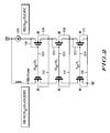
- FIG. 3 is another exemplary integrated MOS stacked circuit device.
- FIG. 4 is an exemplary isolated p-well device.
- FIG. 5 is an exemplary low noise amplifier on an MOS integrated circuit.
- FIG. 6 is an alternative exemplary integrated MOS stacked circuit.
- an integrated NMOS circuit comprises generally an active stack having a plurality of active devices M 4 , M 5 and M 6 , shown single-ended but could represent a simplification of a differential embodiment, and a bias stack with a corresponding plurality of diode-connected bias devices M 1 , M 2 and M 3 .
- the circuit is configured for optimal bias and minimal supply voltage, V DD , within the scope of the invention, as discussed more fully below.
- the devices of the active stack and the bias stack are preferably isolated p-well devices, which are fabricated with triple-well process technology known by those having ordinary skill in the art.
- FIG. 4 illustrates an isolated p-well device 10 comprising generally a source 20 , a gate 30 and a drain 40 on an isolated p-well or, bulk, 50 having a contact 52 .
- the bulk 50 is separated from a substrate 60 by an isolated Nwell 70 and a surrounding Nwell 80 having contacts 82 and 83 .
- the gate of each of the plurality of diode-connected isolated p-well bias devices is coupled to the gate of a corresponding one of the plurality of isolated p-well active devices by a corresponding lead 100 , 102 and 104 , respectively.
- the exemplary coupling is direct, but more generally the coupling of the gates may be indirect, for example there may be passive or active circuit components therebetween.
- each diode-connected isolated p-well bias device The voltage between the source and bulk of each diode-connected isolated p-well bias device is reduced to zero by directly connecting the bulk of each diode-connected isolated p-well bias device to the source of the corresponding diode-connected isolated p-well bias device.
- the direct connection between the bulk and the source of each device is made by a corresponding interconnection or lead 106 , 108 and 110 .
- the lead is part of the integrated circuit.
- each of the plurality of diode-connected isolated p-well bias devices is coupled directly to the bulk of the corresponding one of the plurality of isolated p-well active devices by a corresponding lead 112 , 114 and 116 .
- This connection reduces parasitic capacitance.
- the bulk of each of the plurality of isolated p-well active devices is coupled to its source, but this alternative connection increases the parasitic capacitance on the sources versus coupling the bulk of the active device to the bulk of the corresponding bias device.
- a lowermost isolated p-well active device, M 4 , of the active stack is a current source.
- a diode connection is made as follows: the drain of each of the plurality of diode-connected isolated p-well bias devices, M 1 , M 2 and M 2 , is coupled directly to the corresponding gate of the diode-connected isolated p-well bias device by corresponding interconnection 118 , 120 and 122 .
- the bottommost diode-connected isolated p-well bias device M 1 of the bias stack has its gate coupled directly to the gate of a next higher diode-connected isolated p-well bias device M 2 by interconnection 124 , thereby providing the same voltage on the gates of the diode-connected isolated p-well bias devices M 1 and M 2 , which reduces the minimum circuit supply voltage as discussed more fully below.
- the drain of each of the plurality of diode-connected isolated p-well bias devices, M 2 and M 3 , other than the bottommost diode-connected isolated p-well bias device, M 1 is coupled directly to the gate of the corresponding diode-connected isolated p-well bias device by corresponding interconnection 118 and 120 .
- a current source 126 is coupled between the supply voltage and the bias stack. Also, the areas of the active devices are commonly larger than those of the corresponding bias stack devices to reduce the required magnitude of current source 126 by the ratio of areas.
- V OD is the same for all of the diode-connected isolated p-well bias devices.
- V OD V GS ⁇ V T .
- FIG. 5 is an exemplary differential low noise amplifier on a MOS integrated circuit comprising generally an amplifier stack having a plurality of isolated p-well active devices and a bias stack having a plurality of diode-connected isolated p-well bias devices.
- the active stack may be a mixer or op-Amp or some other device stack.
- the gate of each of the plurality of isolated p-well active devices is coupled to the gate of at least one of the plurality of diode-connected isolated p-well devices
- the bulk of each of the plurality of isolated p-well active devices is coupled to the bulk of at least one of the plurality of diode-connected isolated p-well devices
- the source of each of the plurality of diode-connected isolated p-well bias devices is coupled directly to the bulk of the corresponding diode-connected isolated p-well bias device.
- the plurality of isolated p-well active devices comprises first and second isolated p-well active devices 202 and 204 having their bodies coupled to the bulk of a corresponding common diode-connected isolated p-well bias device 206 by interconnection 208 .
- the plurality of isolated p-well active devices also comprises third and fourth isolated p-well active devices 210 and 212 having their gates coupled to the gate and their bodies coupled to the bulk of a corresponding common diode-connected isolated p-well bias device 214 by interconnection 216 and 226 , respectively.
- the drain of the first isolated p-well active device 202 is coupled to the source of the third isolated p-well active device 210
- the drain of the second isolated p-well active device 204 is coupled to the source of the fourth isolated p-well active device 212 forming what is commonly known as a cascode.
- the drain of an isolated p-well current source 218 is coupled to the sources of the first and second isolated p-well active devices 202 and 204 through exemplary degenerating inductors 228 and 230 .
- the isolated p-well current source 218 has its gate coupled to the gate of a corresponding diode-connected isolated p-well bias device 220 of the bias stack.
- the gate of the diode-connected isolated p-well bias device 220 coupled to the gate of the isolated p-well current source 218 , is coupled to the drain of a next higher diode-connected isolated p-well bias device 206 in the bias stack.
- the drain of each of the plurality of diode-connected isolated p-well bias devices 206 and 214 , other than the diode-connected isolated p-well bias device 220 coupled to the isolated p-well current source, is coupled directly to the gate of the corresponding diode-connected isolated p-well bias device.
- corresponding signal isolation devices 222 and 224 interconnect the gate of the first and second isolated p-well active devices 202 and 204 to the gate of the corresponding isolated p-well bias device 206 .
- Each of the isolation devices 222 and 224 is a PMOS device having its gate coupled to ground to turn on the device. The signal isolation could just as well be accomplished with a passive device.
- the input signal is applied across the gates of first and second isolated p-well active devices 202 and 204 through exemplary inductors 232 and 234 .
- the output signal is taken across the drains of the third and fourth isolated p-well active devices 210 and 212 , which have corresponding exemplary loads 236 and 238 isolating the output signal from the positive supply (VDD) while at the same time coupling the DC voltage to the drains of active devices 210 and 212 .
- FIG. 6 is another alternative embodiment wherein the diode-connected isolated p-well bias devices have a forward bulk to source bias.
- the bulk of each of the-plurality of diode-connected isolated p-well bias devices is coupled directly to the bulk of the corresponding one of the plurality of isolated p-well active devices by interconnections 140 , 142 and 144 , respectively.
- each active device and the corresponding bias device are coupled by interconnections 100 , 102 and 104 , respectively, as discussed above in the embodiment of FIG. 3 .
- the bulk to source forward bias in FIG. 6 is provided by directly coupling the drain of each of the plurality of diode-connected isolated p-well bias devices, except the lowermost diode-connected isolated p-well device of the bias stack, to the bulk of the corresponding diode-connected isolated p-well bias device by corresponding interconnection 150 and 152 , respectively.
- the bulk of the lowermost diode-connected isolated p-well bias device is coupled to the bulk of an adjacent diode-connected p-well bias device by interconnect 154
- the gate of the lowermost diode-connected isolated p-well bias device is coupled to the gate of the adjacent diode-connected isolated p-well bias device by interconnect 156 .
- interconnects 158 and 159 interconnect the drain and gate of the two uppermost diode-connected isolated p-well devices, respectively, as discussed above.
- the lowermost isolated p-well active device M 4 of the active stack is a current source.
Abstract
Description
Claims (15)
Priority Applications (3)
| Application Number | Priority Date | Filing Date | Title |
|---|---|---|---|
| US09/972,274 US6630700B2 (en) | 2001-10-05 | 2001-10-05 | NMOS circuit in isolated wells that are connected by a bias stack having pluralirty of diode elements |
| PCT/US2002/030340 WO2003032396A1 (en) | 2001-10-05 | 2002-09-25 | Stacked nmos device biasing on mos integrated circuits and methods therefor |
| TW091122987A TW591789B (en) | 2001-10-05 | 2002-10-04 | An integrated NMOS circuit, a low noise amplifier, and a method of biasing in an integrated NMOS circuit |
Applications Claiming Priority (1)
| Application Number | Priority Date | Filing Date | Title |
|---|---|---|---|
| US09/972,274 US6630700B2 (en) | 2001-10-05 | 2001-10-05 | NMOS circuit in isolated wells that are connected by a bias stack having pluralirty of diode elements |
Publications (2)
| Publication Number | Publication Date |
|---|---|
| US20030067042A1 US20030067042A1 (en) | 2003-04-10 |
| US6630700B2 true US6630700B2 (en) | 2003-10-07 |
Family
ID=25519445
Family Applications (1)
| Application Number | Title | Priority Date | Filing Date |
|---|---|---|---|
| US09/972,274 Expired - Fee Related US6630700B2 (en) | 2001-10-05 | 2001-10-05 | NMOS circuit in isolated wells that are connected by a bias stack having pluralirty of diode elements |
Country Status (3)
| Country | Link |
|---|---|
| US (1) | US6630700B2 (en) |
| TW (1) | TW591789B (en) |
| WO (1) | WO2003032396A1 (en) |
Cited By (1)
| Publication number | Priority date | Publication date | Assignee | Title |
|---|---|---|---|---|
| US20040217442A1 (en) * | 2001-07-30 | 2004-11-04 | Hiroshi Miyagi | Semiconductor device |
Families Citing this family (11)
| Publication number | Priority date | Publication date | Assignee | Title |
|---|---|---|---|---|
| US7429891B2 (en) * | 2003-02-14 | 2008-09-30 | Broadcom Corporation | Method and system for low noise amplifier (LNA) gain adjustment through narrowband received signal strength indicator (NRSSI) |
| US7129745B2 (en) * | 2004-05-19 | 2006-10-31 | Altera Corporation | Apparatus and methods for adjusting performance of integrated circuits |
| US7348827B2 (en) * | 2004-05-19 | 2008-03-25 | Altera Corporation | Apparatus and methods for adjusting performance of programmable logic devices |
| US20060119382A1 (en) * | 2004-12-07 | 2006-06-08 | Shumarayev Sergey Y | Apparatus and methods for adjusting performance characteristics of programmable logic devices |
| US7495471B2 (en) | 2006-03-06 | 2009-02-24 | Altera Corporation | Adjustable transistor body bias circuitry |
| US7330049B2 (en) * | 2006-03-06 | 2008-02-12 | Altera Corporation | Adjustable transistor body bias generation circuitry with latch-up prevention |
| US7355437B2 (en) * | 2006-03-06 | 2008-04-08 | Altera Corporation | Latch-up prevention circuitry for integrated circuits with transistor body biasing |
| US20080272394A1 (en) * | 2007-05-01 | 2008-11-06 | Ashok Kumar Kapoor | Junction field effect transistors in germanium and silicon-germanium alloys and method for making and using |
| US8018286B2 (en) | 2009-02-12 | 2011-09-13 | Iptronics A/S | Low power integrated circuit |
| US9543916B2 (en) | 2014-06-19 | 2017-01-10 | Project Ft, Inc. | Active device which has a high breakdown voltage, is memory-less, traps even harmonic signals and circuits used therewith |
| WO2016112125A1 (en) | 2015-01-06 | 2016-07-14 | Project Ft, Inc. | Memoryless common-mode insensitive and low pulling vco |
Citations (3)
| Publication number | Priority date | Publication date | Assignee | Title |
|---|---|---|---|---|
| US6111282A (en) | 1995-10-31 | 2000-08-29 | Micron Technology, Inc. | Charge-pumping to increase electron collection efficiency |
| US6388483B1 (en) * | 1995-03-29 | 2002-05-14 | Hitachi, Ltd. | Semiconductor integrated circuit device and microcomputer |
| US6521946B2 (en) | 2000-11-30 | 2003-02-18 | Texas Instruments Incorporated | Electrostatic discharge resistant extended drain metal oxide semiconductor transistor |
-
2001
- 2001-10-05 US US09/972,274 patent/US6630700B2/en not_active Expired - Fee Related
-
2002
- 2002-09-25 WO PCT/US2002/030340 patent/WO2003032396A1/en not_active Application Discontinuation
- 2002-10-04 TW TW091122987A patent/TW591789B/en not_active IP Right Cessation
Patent Citations (3)
| Publication number | Priority date | Publication date | Assignee | Title |
|---|---|---|---|---|
| US6388483B1 (en) * | 1995-03-29 | 2002-05-14 | Hitachi, Ltd. | Semiconductor integrated circuit device and microcomputer |
| US6111282A (en) | 1995-10-31 | 2000-08-29 | Micron Technology, Inc. | Charge-pumping to increase electron collection efficiency |
| US6521946B2 (en) | 2000-11-30 | 2003-02-18 | Texas Instruments Incorporated | Electrostatic discharge resistant extended drain metal oxide semiconductor transistor |
Non-Patent Citations (5)
| Title |
|---|
| Arvin R. Shahani, Derek K. Shaeffer, and Thomas H. Lee, A 12-mW Wide Dynamic Range CMOS Front-End for a Portable GPS Receiver, IEEE Journal of Solid-State Circuits, vol. 32, No. 12, Dec. 1997, pp. 2061-2070. |
| Chi-Nan Brian Li, Didier Farenc, Rana Singh, Jane Yater, Sarah Liu, Chia-Lin Chang, Sandeep Bagchi, Kevin Chen, Paul Ingersoll and Kuo-Tung Chang, A Novel Uniform-Channel-Program-Erase (UCPE) Flash EEPROM Using An Isolated P-well Structure, IEDM Tech. Digest, No. 33.5.1-33.5.4, Apr. 2000, pp. 779-782. |
| Ming-Jer Chen, Jih-Shin Ho, Tzuen-His Huang, Chuang-Hen Yang, Yeh-Ning Jou, and Terry Wu, Back-Gate Forward Bias Method for Low-Voltage CMOS Digital Circuits, IEEE Transactions on Electron Devices, vol. 43, No. 6, Jun. 1996, pp. 904-910. |
| PCT/US02/30340 PCT Search Report mailed Mar. 7, 2003. |
| Torsten Lehmann and Marco Cassia, 1-V Power Supply CMOS Cascode Amplifier, IEEE Journal of Solid-State Circuits, vol. 36, No. 7, Jul. 2001, pp. 1082-1086. |
Cited By (1)
| Publication number | Priority date | Publication date | Assignee | Title |
|---|---|---|---|---|
| US20040217442A1 (en) * | 2001-07-30 | 2004-11-04 | Hiroshi Miyagi | Semiconductor device |
Also Published As
| Publication number | Publication date |
|---|---|
| US20030067042A1 (en) | 2003-04-10 |
| TW591789B (en) | 2004-06-11 |
| WO2003032396A1 (en) | 2003-04-17 |
Similar Documents
| Publication | Publication Date | Title |
|---|---|---|
| US7990667B2 (en) | Semiconductor device including esd protection field effect transistor with adjustable back gate potential | |
| US7221190B2 (en) | Differential comparator with extended common mode voltage range | |
| US20030173594A1 (en) | Voltage converter having switching element with variable substrate potential | |
| US6630700B2 (en) | NMOS circuit in isolated wells that are connected by a bias stack having pluralirty of diode elements | |
| US10627847B2 (en) | Bias current circuit operating at high and low voltages | |
| US6005439A (en) | Unity gain signal amplifier | |
| US20140176230A1 (en) | High-Voltage Tolerant Biasing Arrangement Using Low-Voltage Devices | |
| US5973544A (en) | Intermediate potential generation circuit | |
| JPH10173499A (en) | Output driver circuit and semiconductor device | |
| US8008951B2 (en) | High voltage switch utilizing low voltage MOS transistors with high voltage breakdown isolation junctions | |
| US6762646B1 (en) | Modified folded cascode amplifier | |
| US6573752B1 (en) | High voltage push-pull driver on standard CMOS | |
| US7064609B1 (en) | High voltage, low-offset operational amplifier with rail-to-rail common mode input range in a digital CMOS process | |
| US20090261867A1 (en) | Semiconductor device having voltage output circuit | |
| US20170213831A1 (en) | Operational amplifier circuit | |
| US7196379B2 (en) | MOS capacitor device | |
| US5923212A (en) | Bias generator for a low current divider | |
| US20070146063A1 (en) | Differential amplifier circuit operable with wide range of input voltages | |
| US6563447B1 (en) | Non-linear bulk capacitance bootstrapped current switch | |
| US7667503B2 (en) | Semiconductor switching circuit with hysteresis | |
| JP4654666B2 (en) | Analog switch circuit | |
| US6445250B1 (en) | Circuit topology for better supply immunity in a cascaded Gm/Gm amplifier | |
| CN108628379B (en) | Bias circuit | |
| US6545506B1 (en) | CMOS output driver that can tolerant a high input voltage | |
| JPS62229416A (en) | Voltage limit circuit |
Legal Events
| Date | Code | Title | Description |
|---|---|---|---|
| AS | Assignment |
Owner name: MOTOROLA, INC., ILLINOIS Free format text: ASSIGNMENT OF ASSIGNORS INTEREST;ASSIGNOR:KAATZ, GARY;REEL/FRAME:012248/0431 Effective date: 20011001 |
|
| AS | Assignment |
Owner name: FREESCALE SEMICONDUCTOR, INC., TEXAS Free format text: ASSIGNMENT OF ASSIGNORS INTEREST;ASSIGNOR:MOTOROLA, INC.;REEL/FRAME:015698/0657 Effective date: 20040404 Owner name: FREESCALE SEMICONDUCTOR, INC.,TEXAS Free format text: ASSIGNMENT OF ASSIGNORS INTEREST;ASSIGNOR:MOTOROLA, INC.;REEL/FRAME:015698/0657 Effective date: 20040404 |
|
| AS | Assignment |
Owner name: CITIBANK, N.A. AS COLLATERAL AGENT, NEW YORK Free format text: SECURITY AGREEMENT;ASSIGNORS:FREESCALE SEMICONDUCTOR, INC.;FREESCALE ACQUISITION CORPORATION;FREESCALE ACQUISITION HOLDINGS CORP.;AND OTHERS;REEL/FRAME:018855/0129 Effective date: 20061201 Owner name: CITIBANK, N.A. AS COLLATERAL AGENT,NEW YORK Free format text: SECURITY AGREEMENT;ASSIGNORS:FREESCALE SEMICONDUCTOR, INC.;FREESCALE ACQUISITION CORPORATION;FREESCALE ACQUISITION HOLDINGS CORP.;AND OTHERS;REEL/FRAME:018855/0129 Effective date: 20061201 |
|
| REMI | Maintenance fee reminder mailed | ||
| LAPS | Lapse for failure to pay maintenance fees | ||
| STCH | Information on status: patent discontinuation |
Free format text: PATENT EXPIRED DUE TO NONPAYMENT OF MAINTENANCE FEES UNDER 37 CFR 1.362 |
|
| FP | Lapsed due to failure to pay maintenance fee |
Effective date: 20071007 |
|
| AS | Assignment |
Owner name: FREESCALE SEMICONDUCTOR, INC., TEXAS Free format text: PATENT RELEASE;ASSIGNOR:CITIBANK, N.A., AS COLLATERAL AGENT;REEL/FRAME:037354/0225 Effective date: 20151207 |