JP2007528941A - Coated body and method for coating substrate - Google Patents
Coated body and method for coating substrate Download PDFInfo
- Publication number
- JP2007528941A JP2007528941A JP2007503022A JP2007503022A JP2007528941A JP 2007528941 A JP2007528941 A JP 2007528941A JP 2007503022 A JP2007503022 A JP 2007503022A JP 2007503022 A JP2007503022 A JP 2007503022A JP 2007528941 A JP2007528941 A JP 2007528941A
- Authority
- JP
- Japan
- Prior art keywords
- coating layer
- coating
- alumina
- substrate
- kappa
- Prior art date
- Legal status (The legal status is an assumption and is not a legal conclusion. Google has not performed a legal analysis and makes no representation as to the accuracy of the status listed.)
- Ceased
Links
Images


Classifications
-
- C—CHEMISTRY; METALLURGY
- C23—COATING METALLIC MATERIAL; COATING MATERIAL WITH METALLIC MATERIAL; CHEMICAL SURFACE TREATMENT; DIFFUSION TREATMENT OF METALLIC MATERIAL; COATING BY VACUUM EVAPORATION, BY SPUTTERING, BY ION IMPLANTATION OR BY CHEMICAL VAPOUR DEPOSITION, IN GENERAL; INHIBITING CORROSION OF METALLIC MATERIAL OR INCRUSTATION IN GENERAL
- C23C—COATING METALLIC MATERIAL; COATING MATERIAL WITH METALLIC MATERIAL; SURFACE TREATMENT OF METALLIC MATERIAL BY DIFFUSION INTO THE SURFACE, BY CHEMICAL CONVERSION OR SUBSTITUTION; COATING BY VACUUM EVAPORATION, BY SPUTTERING, BY ION IMPLANTATION OR BY CHEMICAL VAPOUR DEPOSITION, IN GENERAL
- C23C16/00—Chemical coating by decomposition of gaseous compounds, without leaving reaction products of surface material in the coating, i.e. chemical vapour deposition [CVD] processes
- C23C16/22—Chemical coating by decomposition of gaseous compounds, without leaving reaction products of surface material in the coating, i.e. chemical vapour deposition [CVD] processes characterised by the deposition of inorganic material, other than metallic material
- C23C16/30—Deposition of compounds, mixtures or solid solutions, e.g. borides, carbides, nitrides
- C23C16/40—Oxides
- C23C16/403—Oxides of aluminium, magnesium or beryllium
-
- C—CHEMISTRY; METALLURGY
- C23—COATING METALLIC MATERIAL; COATING MATERIAL WITH METALLIC MATERIAL; CHEMICAL SURFACE TREATMENT; DIFFUSION TREATMENT OF METALLIC MATERIAL; COATING BY VACUUM EVAPORATION, BY SPUTTERING, BY ION IMPLANTATION OR BY CHEMICAL VAPOUR DEPOSITION, IN GENERAL; INHIBITING CORROSION OF METALLIC MATERIAL OR INCRUSTATION IN GENERAL
- C23C—COATING METALLIC MATERIAL; COATING MATERIAL WITH METALLIC MATERIAL; SURFACE TREATMENT OF METALLIC MATERIAL BY DIFFUSION INTO THE SURFACE, BY CHEMICAL CONVERSION OR SUBSTITUTION; COATING BY VACUUM EVAPORATION, BY SPUTTERING, BY ION IMPLANTATION OR BY CHEMICAL VAPOUR DEPOSITION, IN GENERAL
- C23C16/00—Chemical coating by decomposition of gaseous compounds, without leaving reaction products of surface material in the coating, i.e. chemical vapour deposition [CVD] processes
- C23C16/02—Pretreatment of the material to be coated
- C23C16/0272—Deposition of sub-layers, e.g. to promote the adhesion of the main coating
-
- C—CHEMISTRY; METALLURGY
- C23—COATING METALLIC MATERIAL; COATING MATERIAL WITH METALLIC MATERIAL; CHEMICAL SURFACE TREATMENT; DIFFUSION TREATMENT OF METALLIC MATERIAL; COATING BY VACUUM EVAPORATION, BY SPUTTERING, BY ION IMPLANTATION OR BY CHEMICAL VAPOUR DEPOSITION, IN GENERAL; INHIBITING CORROSION OF METALLIC MATERIAL OR INCRUSTATION IN GENERAL
- C23C—COATING METALLIC MATERIAL; COATING MATERIAL WITH METALLIC MATERIAL; SURFACE TREATMENT OF METALLIC MATERIAL BY DIFFUSION INTO THE SURFACE, BY CHEMICAL CONVERSION OR SUBSTITUTION; COATING BY VACUUM EVAPORATION, BY SPUTTERING, BY ION IMPLANTATION OR BY CHEMICAL VAPOUR DEPOSITION, IN GENERAL
- C23C16/00—Chemical coating by decomposition of gaseous compounds, without leaving reaction products of surface material in the coating, i.e. chemical vapour deposition [CVD] processes
- C23C16/44—Chemical coating by decomposition of gaseous compounds, without leaving reaction products of surface material in the coating, i.e. chemical vapour deposition [CVD] processes characterised by the method of coating
- C23C16/52—Controlling or regulating the coating process
-
- C—CHEMISTRY; METALLURGY
- C23—COATING METALLIC MATERIAL; COATING MATERIAL WITH METALLIC MATERIAL; CHEMICAL SURFACE TREATMENT; DIFFUSION TREATMENT OF METALLIC MATERIAL; COATING BY VACUUM EVAPORATION, BY SPUTTERING, BY ION IMPLANTATION OR BY CHEMICAL VAPOUR DEPOSITION, IN GENERAL; INHIBITING CORROSION OF METALLIC MATERIAL OR INCRUSTATION IN GENERAL
- C23C—COATING METALLIC MATERIAL; COATING MATERIAL WITH METALLIC MATERIAL; SURFACE TREATMENT OF METALLIC MATERIAL BY DIFFUSION INTO THE SURFACE, BY CHEMICAL CONVERSION OR SUBSTITUTION; COATING BY VACUUM EVAPORATION, BY SPUTTERING, BY ION IMPLANTATION OR BY CHEMICAL VAPOUR DEPOSITION, IN GENERAL
- C23C28/00—Coating for obtaining at least two superposed coatings either by methods not provided for in a single one of groups C23C2/00 - C23C26/00 or by combinations of methods provided for in subclasses C23C and C25C or C25D
- C23C28/02—Coating for obtaining at least two superposed coatings either by methods not provided for in a single one of groups C23C2/00 - C23C26/00 or by combinations of methods provided for in subclasses C23C and C25C or C25D only coatings only including layers of metallic material
- C23C28/023—Coating for obtaining at least two superposed coatings either by methods not provided for in a single one of groups C23C2/00 - C23C26/00 or by combinations of methods provided for in subclasses C23C and C25C or C25D only coatings only including layers of metallic material only coatings of metal elements only
-
- C—CHEMISTRY; METALLURGY
- C23—COATING METALLIC MATERIAL; COATING MATERIAL WITH METALLIC MATERIAL; CHEMICAL SURFACE TREATMENT; DIFFUSION TREATMENT OF METALLIC MATERIAL; COATING BY VACUUM EVAPORATION, BY SPUTTERING, BY ION IMPLANTATION OR BY CHEMICAL VAPOUR DEPOSITION, IN GENERAL; INHIBITING CORROSION OF METALLIC MATERIAL OR INCRUSTATION IN GENERAL
- C23C—COATING METALLIC MATERIAL; COATING MATERIAL WITH METALLIC MATERIAL; SURFACE TREATMENT OF METALLIC MATERIAL BY DIFFUSION INTO THE SURFACE, BY CHEMICAL CONVERSION OR SUBSTITUTION; COATING BY VACUUM EVAPORATION, BY SPUTTERING, BY ION IMPLANTATION OR BY CHEMICAL VAPOUR DEPOSITION, IN GENERAL
- C23C30/00—Coating with metallic material characterised only by the composition of the metallic material, i.e. not characterised by the coating process
- C23C30/005—Coating with metallic material characterised only by the composition of the metallic material, i.e. not characterised by the coating process on hard metal substrates
Abstract
基体(22)および前記基体上のコーティングスキーム(32)を含むコーティング体。基体(22)上のコーティングスキーム(32)は、その表面で小板粒子形態を示すアルファ−アルミナコーティング層(40)またはその表面でレンズ形粒子形態または多角−レンズ形粒子形態のいずれかを示すカッパアルミナコーティング層(40)またはその表面で大多面粒子形態または多角−多面粒子形態のいずれかを示すアルファ−カッパ−アルミナコーティング層(40)を含む。 Coated body comprising a substrate (22) and a coating scheme (32) on said substrate. The coating scheme (32) on the substrate (22) exhibits either an alpha-alumina coating layer (40) that exhibits platelet particle morphology on its surface or either lenticular or polygonal-lens particle morphology on its surface. It includes a kappa alumina coating layer (40) or an alpha-kappa-alumina coating layer (40) that exhibits either a large polyhedral or polygonal-polyhedral particle morphology on its surface.
Description
本発明は、アルミナコーティングおよびコーティングされた製品、特に、物質除去用途、例えば、機械加工、旋削、および粉砕において有用な、コーティングされたカッティングインサートに関する。さらに詳細には、本発明は、コーティングがアルファ−アルミナまたはカッパ−アルミナまたはアルファおよびカッパ−アルミナの混合物のコーティング層を含む、コーティングされたカッティングインサート、ならびに前記コーティングおよびコーティングされたカッティングインサートの製造法に関する。 The present invention relates to coated coating inserts useful in alumina coatings and coated products, particularly in material removal applications such as machining, turning and grinding. More particularly, the present invention relates to a coated cutting insert, wherein the coating comprises a coating layer of alpha-alumina or kappa-alumina or a mixture of alpha and kappa-alumina, and a method for producing said coated and coated cutting insert. About.
従来、物質を除去する用途においてコーティングされたカッティングインサートが用いられてきた。コーティング層は典型的には、耐摩耗性を示す硬質耐熱性物質を含む。カッティングインサート上にコーティングを使用する主な目的の一つは、カッティングインサートの有効寿命を延長することである。コーティングスキームがアルミナのコーティング層を含む、このようなコーティングスキームの例は、多くの特許文献において開示されており、これらの特許文献の一例を以下に記載する。 Traditionally, coated cutting inserts have been used in materials removal applications. The coating layer typically includes a hard refractory material that exhibits abrasion resistance. One of the main purposes of using a coating on a cutting insert is to extend the useful life of the cutting insert. Examples of such coating schemes, where the coating scheme includes an alumina coating layer, are disclosed in many patent documents, examples of which are described below.
特許文献1(Ishiiら)は、その上にα−アルミナ層が堆積される酸化層を有することが有益であると認識しているようである。特許文献2は(Chudoら)は、TiCOまたはTiCNOがアルミナ層の接着を向上させることができることに言及している。 U.S. Patent No. 5,099,086 (Ishii et al.) Appears to recognize that it is beneficial to have an oxide layer on which an α-alumina layer is deposited. U.S. Patent No. 6,057,059 (Chudo et al.) Mentions that TiCO or TiCNO can improve the adhesion of the alumina layer.
特許文献3は(Nakamuraら)は、TiCNO層およびTiCO層上に900℃でアルミナを蒸着させることを示しているようである。この特許は、多層コーティングスキームを示しているようである。特許文献4(三菱マテリアル株式会社)(および特許文献5(Ichikawaら))は、TiCOまたはTiCNOの堆積およびこれらのTi含有層のいずれか1つの上にアルミナを堆積させることを開示しているようである。特許文献6(三菱マテリアル株式会社)(および特許文献7(Uedaら))は、TiCNO層またはTiCO層上に950℃で設けられたアルミナ層を示しているようである。特許文献8(三菱マテリアル株式会社)は、チタンカルボキシド層またはチタンオキシカルボナイトライド層上のχタイプアルミナのCVD蒸着を開示している。 U.S. Patent No. 6,056,049 (Nakamura et al.) Appears to indicate depositing alumina at 900 ° C on the TiCNO and TiCO layers. This patent appears to show a multilayer coating scheme. Patent Document 4 (Mitsubishi Materials Corporation) (and Patent Document 5 (Ichikawa et al.)) Seems to disclose depositing TiCO or TiCNO and depositing alumina on any one of these Ti-containing layers. It is. Patent Document 6 (Mitsubishi Materials Corporation) (and Patent Document 7 (Ueda et al.)) Seems to show an alumina layer provided at 950 ° C. on a TiCNO layer or a TiCO layer. Patent Document 8 (Mitsubishi Materials Corporation) discloses CVD deposition of χ type alumina on a titanium carboxylide layer or a titanium oxycarbonitride layer.
特許文献9(Sandvik AB)は、Tiを含有する線条領域を持つ等軸粒子を有するアルファ−アルミナ層をTiCNO層上に蒸着するコーティングスキームに関する。このアルファ−アルミナ層の蒸着温度は約1000℃である。 U.S. Patent No. 6,057,028 (Sandvik AB) relates to a coating scheme in which an alpha-alumina layer having equiaxed particles with a striation region containing Ti is deposited on a TiCNO layer. The deposition temperature of this alpha-alumina layer is about 1000 ° C.
特許文献10(Yoshimuraら)は、TiCNO層またはTiCO層上に蒸着されたアルミナを含むコーティングスキームに関する。このアルミナは、850〜1000℃に等しい温度で設けられるようであるが、アルミナはκ−アルミナまたはカッパ含量がアルファ含量よりも高いカッパおよびアルファアルミナの組み合わせのいずれかである。 U.S. Patent No. 6,057,059 (Yoshimura et al.) Relates to a coating scheme comprising alumina deposited on a TiCNO layer or a TiCO layer. The alumina appears to be provided at a temperature equal to 850-1000 ° C., but the alumina is either kappa-alumina or a combination of kappa and alpha alumina where the kappa content is higher than the alpha content.
特許文献11(NGK Spark Plug)は、アルミナ層がTiCNO層上に堆積される例を提示している。特許文献12(三菱マテリアル株式会社)は、バインダー豊富な基体上のコーティングスキームを開示している。このコーティングはTiCOおよびTiCNO上に堆積されたアルミナを含む。
前記文献から明らかなように、多くの異なるカッティングインサート用コーティングスキームが過去において用いられてきた。これらの特許文献によると、これらのコーティングスキームのそれぞれは、ある利点をもたらす。ある利点をもたらすと思われるコーティングスキームがあるにもかかわらず、コーティングされたカッティングインサートの性能特性を改善すると共に有効寿命を延長し続けることが常に望まれている。 As is apparent from the literature, many different cutting insert coating schemes have been used in the past. According to these patent documents, each of these coating schemes provides certain advantages. Despite the coating schemes that appear to provide certain advantages, it is always desirable to improve the performance characteristics of coated cutting inserts and continue to extend their useful life.
かくして、改善されたアルミナコーティングおよびコーティングされた製品、例えば、コーティングがアルファ−アルミナ(またはカッパ−アルミナまたはアルファ−カッパアルミナ)のコーティング層を含み、カッティングインサートが物質除去用途において有用であり、カッティングインサートが延長された工具寿命を有する、コーティングされたカッティングインサートを提供することが非常に望ましいであろう。また、改善されたアルミナコーティングおよびコーティングされた製品、例えば、コーティングがアルファ−アルミナ(またはカッパ−アルミナまたはアルファ−カッパアルミナ)のコーティング層を含み、カッティングインサートが物質除去用途において有用であり、カッティングインサートが改善された性能特性を示す、コーティングされたカッティングインサートを提供することが望ましいであろう。 Thus, improved alumina coatings and coated products, for example, where the coating includes a coating layer of alpha-alumina (or kappa-alumina or alpha-kappa alumina), the cutting insert is useful in material removal applications, and the cutting insert It would be highly desirable to provide a coated cutting insert that has an extended tool life. Also improved alumina coatings and coated products, for example, the coating includes a coating layer of alpha-alumina (or kappa-alumina or alpha-kappa alumina), the cutting insert is useful in material removal applications, and the cutting insert It would be desirable to provide a coated cutting insert that exhibits improved performance characteristics.
その一形態において、本発明は、基体、および前記基体上のコーティングスキームを含むコーティング体である。このコーティングスキームは、その表面で小板粒子形態を示すアルファ−アルミナコーティング層を含む。 In one form thereof, the present invention is a coated body comprising a substrate and a coating scheme on the substrate. This coating scheme includes an alpha-alumina coating layer that exhibits platelet particle morphology on its surface.
別の形態において、本発明は、基体を含むコーティング体である。前記基体上にはコーティングスキームがあり、前記コーティングスキームは、その表面でレンズ形粒子形態または多角レンズ形態のいずれかを示すカッパ−アルミナコーティング層を含む。 In another form, the present invention is a coating body comprising a substrate. There is a coating scheme on the substrate, the coating scheme comprising a kappa-alumina coating layer that exhibits either lenticular particle morphology or polygonal lens morphology on its surface.
さらに別の形態において、本発明は基体を含むコーティング体である。前記基体上にはコーティングスキームがあり、前記コーティングスキームは、アルファ−アルミナおよびカッパ−アルミナを含有するアルミナコーティング層を含み、前記コーティング層は、その表面で、大多面粒子形態または多角−多面粒子形態のいずれかを示す。 In yet another form, the present invention is a coating body comprising a substrate. There is a coating scheme on the substrate, the coating scheme comprising an alumina coating layer containing alpha-alumina and kappa-alumina, the coating layer having a large polyhedral or polygonal-polyhedral particle morphology on its surface. Indicates one of the following.
もう一つ別の形態において、本発明は基体を含むコーティング体である。前記基体上にはコーティングスキームがあり、前記コーティングスキームは、アルファ−アルミナコーティング層およびカッパ−アルミナコーティング層およびカッパ−アルファ−アルミナコーティング層からなる群から選択されるアルミナコーティング層を含み、前記コーティング層は約750℃から約920℃の温度で化学蒸着法により設けられる。 In another form, the present invention is a coating body comprising a substrate. There is a coating scheme on the substrate, the coating scheme comprising an alumina coating layer selected from the group consisting of an alpha-alumina coating layer and a kappa-alumina coating layer and a kappa-alpha-alumina coating layer, wherein the coating layer Is provided by chemical vapor deposition at a temperature of about 750 ° C. to about 920 ° C.
さらに別の形態において、本発明は、約750℃から約920℃の温度で化学蒸着法によりアルファ−アルミナコーティング層を設ける工程を含む、基体をコーティングする方法であり、このアルファ−アルミナコーティング層は、その表面で小板粒子形態を示す。 In yet another aspect, the present invention is a method of coating a substrate comprising the step of providing an alpha-alumina coating layer by chemical vapor deposition at a temperature of about 750 ° C. to about 920 ° C., wherein the alpha-alumina coating layer comprises: The platelet particle morphology is shown on the surface.
さらに別の形態において、本発明は、約750℃から約920℃の温度で化学蒸着法によりカッパ−アルミナコーティング層を設ける工程を含む、基体をコーティングする方法であり、このカッパ−アルミナコーティング層は、その表面でレンズ形粒子形態または多角レンズ形粒子形態のいずれかを示す。 In yet another form, the present invention is a method of coating a substrate comprising the step of providing a kappa-alumina coating layer by chemical vapor deposition at a temperature of about 750 ° C. to about 920 ° C., wherein the kappa-alumina coating layer comprises: , Shows either lenticular particle shape or polygonal lenticular particle morphology on its surface.
さらにもう一つ別の形態において、本発明は、約750℃から約920℃の温度で化学蒸着法によりアルファ−カッパ−アルミナコーティング層を設ける工程を含む、基体をコーティングする方法であり、このアルファ−カッパ−アルミナコーティング層は、その表面で大多面粒子形態または多角−多面粒子形態のいずれかを示す。 In yet another aspect, the present invention is a method of coating a substrate comprising the step of providing an alpha-kappa-alumina coating layer by chemical vapor deposition at a temperature of about 750 ° C. to about 920 ° C. The kappa-alumina coating layer exhibits either a large polyhedral particle morphology or a polygonal-polyhedral particle morphology on its surface.
さらにもう一つ別の形態において、本発明は、多結晶立方晶窒化ホウ素を含む基体を含むコーティング体である。前記基体上にはコーティングスキームがあり、前記コーティングスキームは、アルミナコーティング層を含む。前記アルミナコーティング層は次のもの、すなわち、その表面で小板粒子形態を有するアルファ−アルミナコーティング層、またはその表面でレンズ形粒子形態またはその表面で多角レンズ形粒子形態のいずれかを有するカッパ−アルミナコーティング層、またはその表面で大多面粒子形態またはその表面で多角−多面粒子形態のいずれかを有するアルファ−カッパ−アルミナコーティング層のうちの1つを含む。 In yet another aspect, the present invention is a coating that includes a substrate comprising polycrystalline cubic boron nitride. There is a coating scheme on the substrate, the coating scheme including an alumina coating layer. The alumina coating layer is: an alpha-alumina coating layer having platelet particle morphology on its surface, or a kappa having either lenticular particle morphology on its surface or polygonal lens particle morphology on its surface It includes one of an alumina coating layer, or an alpha-kappa-alumina coating layer having either a large polyhedral particle morphology on its surface or a polygon-polyhedral particle morphology on its surface.
図面に関して、図1および2は、本発明の特定の具体例を説明し、図中、コーティングされたカッティングインサートは全般的に20で示される。コーティングされたカッティングインサート20は基体22を含む。基体22は、多くの基体材料の任意の一つで作ることができる。基体の材料としては、超硬合金、炭化物、セラミック、サーメット、および多結晶立方晶窒化ホウ素(PcBN)が挙げられるが、これらに限定されない。
With reference to the drawings, FIGS. 1 and 2 illustrate particular embodiments of the present invention, in which the coated cutting insert is generally indicated at 20. Coated
超硬合金としては、コバルト含量が最高約15重量%までであるコバルト超硬炭化タングステンや、コバルトのない炭化タングステン基体も含む。超硬(コバルト)タングステンカーバイドの場合、基体は、基体の表面から始まり、表面から内部に伸びるバインダー豊富な領域を示し得る。 Cemented carbides include cobalt cemented tungsten carbide with a cobalt content up to about 15% by weight and tungsten carbide substrates without cobalt. In the case of carbide (cobalt) tungsten carbide, the substrate can exhibit a binder-rich region starting from the surface of the substrate and extending inwardly from the surface.
もう一つの代替案として、超硬合金基体はバインダーが豊富なことを示さない場合がある。超硬合金基体は、1以上の添加剤、例えば、1以上の次の元素および/またはその化合物、すなわち、チタン、ニオブ、バナジウム、タンタル、クロム、ジルコニウムおよび/またはハフニウムも含有することができる。超硬合金基体はその中に窒素も含有することができる。 As another alternative, the cemented carbide substrate may not show that the binder is rich. The cemented carbide substrate may also contain one or more additives, such as one or more of the following elements and / or compounds thereof: titanium, niobium, vanadium, tantalum, chromium, zirconium and / or hafnium. The cemented carbide substrate can also contain nitrogen therein.
セラミックとしては、窒化ケイ素系セラミック、SiAlON系セラミック、炭窒化チタン系セラミック、二ホウ化チタン系セラミックおよびアルミナ系セラミックが挙げられる。サーメットとしては、ニッケル−コバルトバインダーおよび高レベルのチタンを有し、炭化タングステン、および炭化チタンをさらに含み得るものが挙げられる。サーメットは、その中に窒素も含有し得る。 Examples of the ceramic include silicon nitride ceramics, SiAlON ceramics, titanium carbonitride ceramics, titanium diboride ceramics, and alumina ceramics. Cermets include those having a nickel-cobalt binder and a high level of titanium, which may further include tungsten carbide and titanium carbide. The cermet may also contain nitrogen therein.
PcBN材料としては、セラミックまたは金属バインダーを有するものが挙げられる。PcBN材料は、多くの基本的方法においてカッティングインサートとあわせて用いることができる。一つの方法として、PcBNインサートはカッティングインサート本体にろう付けすることができる。別の方法として、PcBNカッティングインサートはフルトップカッティングインサートであり得る。さらに別の方法として、カッティングインサートはPcBNの充実片(solid piece)であり得る。 PcBN materials include those having a ceramic or metal binder. PcBN materials can be used in conjunction with cutting inserts in many basic ways. As one method, the PcBN insert can be brazed to the cutting insert body. Alternatively, the PcBN cutting insert can be a full top cutting insert. As yet another alternative, the cutting insert may be a solid piece of PcBN.
PcBN基体としては、記載された組成を有する次のPcBN材料が挙げられる。 PcBN substrates include the following PcBN materials having the described composition.
PcBN組成No.1は約12重量%のコバルトバインダーおよび約88重量%の立方晶窒化ホウ素に等しい組成を有する。PcBN組成No.1は、典型的には硬鋼および鋳鉄の溝掘り、硬鋼における中程度から重度の断続切削、および/または超合金機械加工に使用される。 PcBN composition No. 1 has a composition equal to about 12% by weight cobalt binder and about 88% by weight cubic boron nitride. PcBN composition No. 1 is typically used for hard steel and cast iron grooving, moderate to heavy interrupted cutting in hard steel, and / or superalloy machining.
PcBN組成No.2は、約50重量%炭化チタンバインダーおよび約50重量%の立方晶窒化ホウ素に等しい組成を有する。PcBN組成No.2は典型的には硬鋼の仕上げ処理に使用される。 PcBN composition No. 2 has a composition equal to about 50 wt% titanium carbide binder and about 50 wt% cubic boron nitride. PcBN composition No. 2 is typically used for finishing of hard steel.
PcBN組成No.3は、窒化アルミニウムおよび炭化ケイ素および二ホウ化チタンを含む約10重量%のバインダー(窒化アルミニウムはバインダーの主成分である)および約90重量%の立方晶窒化ホウ素に等しい組成を有する。 PcBN composition No. 3 has a composition equal to about 10% by weight binder comprising aluminum nitride and silicon carbide and titanium diboride (aluminum nitride is the main component of the binder) and about 90% by weight cubic boron nitride.
PcBN組成No.4は、約18重量%の窒化アルミニウムバインダーおよび約82重量%の立方晶窒化ホウ素に等しい組成を有する。PcBN組成No.3および4を用いるカッティングインサートは、典型的にはPcBNの硬質片であり、かかるカッティングインサートは典型的には、中程度から重度の断続切削のために硬質および軟質鋳鉄上で使用される。 PcBN composition No. 4 has a composition equal to about 18% by weight aluminum nitride binder and about 82% by weight cubic boron nitride. PcBN composition No. Cutting inserts using 3 and 4 are typically hard pieces of PcBN, and such cutting inserts are typically used on hard and soft cast irons for moderate to heavy interrupted cuts.
コーティングされたカッティングインサート20は、逃げ面24およびすくい面26を有する。逃げ面24およびすくい面26は交差して、その交差点でカッティングエッジ28を形成する。コーティングされたカッティングインサート20は、その中に開口部30を含有する。開口部30は、カッティングインサート20をツールホルダーに固定するのに役立つ。
The
コーティングされたカッティングインサート20は、図2においてブラケット32により示されるコーティングスキームを有する。特定のコーティングスキーム32は、4つのコーティング層を含む。これらのコーティング層のそれぞれについて以下に説明する。
Coated cutting
ベースコーティング層34は、化学蒸着法により基体22の表面に設けられる。場合によっては、基体表面をコーティングする前に、例えば、硬質粒子を含有するスラリーによる衝突などにより処理することができる。表面処理の一例は、水およびアルミナ粒子を含むスラリーで表面をウェットブラスティングすることである。他の例においては、表面はコーティング前に処理されない。
The
このコーティングスキームにおいて、ベースコーティング層34は窒化チタンを含むが、ベースコーティング層の組成は、基体に対するコーティングの最良の接着が達成されるように基体材料の組成によって変わり得る。例えば、PcBNまたはセラミックである基体の場合、アルミナのベース層を設けることができる。図1および2のこのコーティングスキームにおいて、このプロセス工程において窒化チタンコーティング層34を蒸着させるために用いられる気体は、H2、N2およびTiCl4である。ベースコーティング層34は、約850℃から約920℃の間の温度で設けることができる。別の範囲として、ベースコーティング層34を、約890℃から約910℃の間の温度で設けることができる。
In this coating scheme, the
ベースコーティング層34を蒸着させるためのプロセスの圧力および時間は、所望のコーティング厚を達成するように変化する。ベースコーティング層34の厚さに関して、一例として、ベースコーティング層34の厚さは0マイクロメートル以上から約3マイクロメートルの間の範囲である。他の範囲としては、ベースコーティング層34の厚さは、0マイクロメートル以上から約1マイクロメートルの範囲である。さらに別の範囲としては、ベースコーティング層34の厚さは、0マイクロメートル以上から約0.5マイクロメートルの範囲である。理解できるように、ベースコーティング層34の特定の厚さは、カッティングインサートの特定の用途に応じて変化し得る。
The process pressure and time for depositing the
中間コーティング層36は、化学蒸着法によりベースコーティング層34上に設けられる。このプロセス工程において用いられる気体は、H2、N2、CH3CNおよびTiCl4である。中間コーティングは、他の気体混合物、例えば、エタンと窒素、およびメタンと窒素、ならびに他の公知の混合物を用いて設けることができる。中間コーティング層36は炭窒化チタンを含む。中間コーティング層36は、約800℃から約920℃の間の範囲の温度で設けられる。他の範囲としては、中間コーティング層36は、約850℃〜約920℃の間の範囲の温度で設けられる。さらに別の範囲としては、中間コーティング層36を、約870℃から約910℃の間の範囲の温度で設けることができる。
The
中間コーティング層36を蒸着させるためのプロセスの圧力および時間は、所望のコーティング厚さを達成するように変化する。この点に関して、中間コーティング層36の厚さは、約1マイクロメートルから約25マイクロメートルの間の範囲である。別の範囲としては、中間コーティング層の厚さは、約3マイクロメートルから約15マイクロメートルの間の範囲である。別の範囲としては、中間コーティングの厚さは、約1マイクロメートルから約5マイクロメートルの間の範囲である。中間コーティング層36の厚さのさらに別の範囲は、約5マイクロメートルから約25マイクロメートルの間である。
The process pressure and time for depositing the
修飾コーティング層38は、化学蒸着法により中間コーティング層36上に設けられる。このプロセス工程において用いることができる気体は、H2、N2およびTiCl4、AlCl3、HCl、CO、CO2およびCH3CNある。修飾コーティング層38は、チタン、アルミニウム、窒素、酸素および炭素を含むことができる。前記元素のすべてが存在する場合、本出願者らは、修飾コーティング層38はチタンアルミニウムオキシカルボナイトライド(TiAlOCN)を含むと考える。しかしながら、修飾層が複数の層を含み、これらの層がチタンオキシカルボナイトライド(TiOCN)および/またはチタンオキシナイトライド(TiON)をチタンアルミニウムオキシカルボナイトライドと共に含む場合がある。修飾コーティング層38は、約750℃から約920℃の間の範囲の温度で設けられる。別の温度範囲として、修飾コーティング層38は、約850℃から約920℃の間の範囲の温度で設けられる。さらに別の温度範囲として、修飾コーティング層38を、約870℃から約890℃の間の範囲の温度で設けることができる。
The modified
修飾コーティング層38を蒸着させるためのプロセスの圧力および時間は、所望のコーティング厚さを達成するように変化する。この点に関して、修飾コーティング層38の厚さは、約0.5マイクロメートルから約5マイクロメートルの間の範囲である。別の範囲として、修飾コーティング層38の厚さは、約0.1マイクロメートルから約1.5マイクロメートルの間の範囲である。
The process pressure and time for depositing the modified
中間コーティング層36と修飾層38の合計厚さは約1マイクロメートルから約30マイクロメートルの間の範囲である。別の範囲として、中間コーティング層36と修飾コーティング層38の合計厚さは、約1.5マイクロメートルから約2.5マイクロメートルの間の範囲である。
The total thickness of the
外側コーティング層40は、化学蒸着法により修飾コーティング層38上に設けられる。このプロセス工程において存在する気体は、H2、N2、AlCl3、HCl、CO、CO2、およびH2Sである。外側コーティング層40はアルミナを含み、アルミナの複数の層を含むことができる。以下の開示から明らかになるように、アルミナ層の結晶相は、アルファ単独、またはカッパ単独またはアルファとカッパ相の混合物を含み得る。本発明により蒸着されたアルファ−アルミナ層の場合、アルファ−アルミナコーティング層40の表面は、その表面で小板粒子形態を示す。本発明により蒸着されたカッパ−アルミナ層の場合、カッパ−アルミナコーティング層40の表面は、その表面でレンズ形粒子形態または多角−レンズ形粒子形態のいずれかを示す。本発明により蒸着されたアルファーカッパ−アルミナ層の場合、アルファ−カッパ−アルミナコーティング層40の表面は、その表面で大多面粒子形態または多角−多面粒子形態のいずれかを示す。
The
アルミナコーティング層40は、約750℃から約920℃の間の範囲の温度で設けられる。アルミナコーティング層40を設けるための他の温度範囲は、約800℃から約920℃の間、約850℃から約920℃の間mおよび約865℃から約895℃の間を含む。
The
外側コーティング層40を蒸着させるためのプロセスの圧力および時間は、所望のコーティング厚さを達成するように変化する。アルミナコーティング層40の厚さの一つの範囲は、約1マイクロメートルから約20マイクロメートルの間である。アルミナコーティング層40の厚さの別の範囲は、約2マイクロメートルから約3マイクロメートルの間である。アルミナコーティング層40の厚さのさらに別の範囲は、約4マイクロメートルから約15マイクロメートルの間である。さらに、アルミナコーティング層40の別の範囲は、約6マイクロメートルから約12マイクロメートルの間である。
The process pressure and time for depositing the
全体的なコーティングスキーム32の合計厚さは、約3マイクロメートルから約40マイクロメートルの間の範囲である。別の範囲として、コーティングスキーム32の全体的な厚さは、約20マイクロメートルから約35マイクロメートルの間の範囲である。別の範囲として、コーティングスキーム32の全体的な厚さは、約8マイクロメートルから約12マイクロメートルの間の範囲である。さらに別の範囲として、コーティングスキームの全体的な厚さは、約5マイクロメートルから約7マイクロメートルの間の範囲である。
The total thickness of the
下記の表1は、コーティングスキームを基体上に蒸着させるための中温化学蒸着(MT−CVD)法の特定の具体例のプロセス工程、すなわち本発明の熱処理No.1を記載する。本発明の熱処理No.1は、図4のカッティングインサート(又は基体)をコーティングするために用いられるMT−CVD法である。本発明の熱処理No.1は、表5において本発明のカッティングインサートとして特定されるカッティングインサートをコーティングするために用いられるプロセスでもある。 Table 1 below shows the process steps of a specific embodiment of a mesothermal chemical vapor deposition (MT-CVD) method for depositing a coating scheme on a substrate, namely heat treatment No. 1 of the present invention. 1 is described. Heat treatment no. 1 is an MT-CVD method used for coating the cutting insert (or substrate) of FIG. Heat treatment no. 1 is also the process used to coat the cutting insert identified in Table 5 as the cutting insert of the present invention.

表1の左から2列目から5列目に特定のコーティング層を記載する。左側の列は、各コーティング層についての4つのプロセスパラメータを提示する。これらのプロセスパラメータは、摂氏度(℃)で表した温度範囲、ミリバール(mb)で表した圧力範囲、コーティング層を蒸着させるための合計時間(または期間)(分)、およびコーティング層の蒸着中に同時に又は別に存在する気体である。表1に記載する特定の方法、すなわち、本発明の熱処理No.1により、表2に記載する次の特性を有するコーティングスキームが製造された。 The specific coating layer is described in the second to fifth columns from the left in Table 1. The left column presents four process parameters for each coating layer. These process parameters include the temperature range in degrees Celsius (° C.), the pressure range in millibars (mb), the total time (or duration) for depositing the coating layer (minutes), and the deposition of the coating layer Gas present simultaneously or separately. The specific method described in Table 1, namely the heat treatment No. 1 of the present invention. 1 produced a coating scheme having the following properties listed in Table 2.
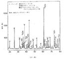
図6は、本発明の熱処理No.1のパラメータによりコーティングされた超硬(コバルト)タングステンカーバイド基体のx線回折パターンである。図6は、外側コーティングがアルファ−アルミナコーティング層であることを示す。SEM顕微鏡写真図4により示されるように、このアルファ−アルミナコーティング層の表面、すなわち、コーティングされたカッティングインサートまたはコーティングされた基体の表面は、小板粒子形態を示すようである。 6 shows the heat treatment No. 1 of the present invention. 1 is an x-ray diffraction pattern of a cemented carbide (cobalt) tungsten carbide substrate coated with a parameter of 1. FIG. 6 shows that the outer coating is an alpha-alumina coating layer. SEM micrograph As shown by FIG. 4, the surface of this alpha-alumina coating layer, ie, the surface of the coated cutting insert or coated substrate, appears to exhibit platelet particle morphology.
本発明の熱処理No.1によりコーティングされたカッティングインサートを、標準的化学蒸着法によりコーティングされた従来技術のコーティングされたカッティングインサートと比較した。標準的化学蒸着コーティング手順は、窒化チタンのベース層を超硬(コバルト)タングステンカーバイド基体上に設け、炭窒化チタンの層を含む中間コーティングスキームを前記ベース層上に設け、チタン、アルミニウム、炭素、窒素および酸素を含むブレンドされたコーティング層を中間コーティングスキーム上に設け、アルミナ層をブレンドされたコーティング層上に設ける工程を含んでいた。中間コーティング層の一部およびブレンドされた層の全部およびアルファ−アルミナコーティング層の全部を化学蒸着法により、約1000℃の温度で設けた。以下の表3は、前記従来法により製造されたコーティングスキームの選択された特性を示す。 Heat treatment no. The cutting insert coated with 1 was compared with a prior art coated cutting insert coated by standard chemical vapor deposition. A standard chemical vapor deposition coating procedure consists of providing a titanium nitride base layer on a carbide (cobalt) tungsten carbide substrate, an intermediate coating scheme comprising a layer of titanium carbonitride on the base layer, titanium, aluminum, carbon, Providing a blended coating layer containing nitrogen and oxygen on the intermediate coating scheme and providing an alumina layer on the blended coating layer. A portion of the intermediate coating layer and all of the blended layer and all of the alpha-alumina coating layer were applied by chemical vapor deposition at a temperature of about 1000 ° C. Table 3 below shows selected properties of the coating scheme produced by the conventional method.
従来技術のカッティングインサートのアルミナコーティング層の表面は、SEM顕微鏡写真図5により示されるような塊状の外観を有する。 The surface of the alumina coating layer of the prior art cutting insert has a massive appearance as shown by the SEM micrograph FIG.
本発明の熱処理No.1のプロセスに従ってコーティングされた本発明のカッティングインサートおよび前記の従来技術のプロセスに従ってコーティングされた従来技術のコーティングされたカッティングインサートを比較する切削試験を行った。本発明のカッティングインサートおよび従来技術のカッティングインサートのどちらの基体も、炭化タングステン(残余)−6重量%のコバルト−0.4重量%のクロムを含んでいた。試験のパラメータは次のとおりであった。インサートスタイル:SPHX1205PCERGPB、カッター:100B08RP90SP12C2WUFP、リード角度:0度、加工品:灰色鋳鉄(クラス40、孔を有するブロック)、操作:フライカットフェースミリング、速度:1200表面フィート/分(393.4表面メートル/分)、供給:0.01インチ/トゥース(ipt)(0.254ミリメートル/トゥース)、カットの深さ:半径方向=3インチ(7.62センチメートル)、および軸方向=0.08インチ(2.03ミリメートル)、冷却剤:乾燥、長さ/パス:24インチ(61センチメートル)。破壊基準は次の通りであった。逃げ面磨耗=0.012インチ(0.305ミリメートル)、最大磨耗およびノーズ磨耗=0.016インチ(0.406ミリメートル)、切削された切り欠き部の深さ(DOCN)=0.02インチ(0.508ミリメートル)、クレーター磨耗=0.004インチ(0.102ミリメートル)。これらの試験に関して、故障モードは、最大逃げ面磨耗およびノーズ磨耗であった。試験結果を下記の表4および5に記載する。
Heat treatment no. A cutting test was performed comparing the cutting insert of the present invention coated according to one process and a prior art coated cutting insert coated according to the prior art process described above. The substrates of both the cutting inserts of the present invention and the prior art cutting inserts contained tungsten carbide (remainder) —6 wt% cobalt—0.4 wt% chromium. The test parameters were as follows: Insert Style: SPHX1205PCERGPB, Cutter: 100B08RP90SP12C2WUFP, Lead Angle: 0 degree, Workpiece: Gray Cast Iron (
表4および5に関して、第1列はコーティングスキームの形成前の基体の状態を記載する。「基準として」なる用語は、基体の表面がコーティングの形成前に処理されていなかったことを意味する。「ブラストされたアルミナスラリー」なる用語は、基体の表面が、アルミナ粒子および水のスラリーによりブラスティングされたことを意味する。第2列は、カッティングエッジがホーンされている(磨かれた)だけであるか、またはT−ランドを有し、且つホーンされているかのいずれかであるカッティングインサートのエッジ調製を記載する。第3列から第5列は、3つの独立した試験のそれぞれについて破損するまでのパスの数を記載する(故障モードは最大逃げ面磨耗およびノーズ磨耗であった)。第6列は、破損するまでのパスの平均数を記載する。表5において、第7列は、前記の従来技術のカッティングインサートの性能と比較した、本発明の熱処理No.1によりコーティングされたカッティングインサートの改善のパーセンテージを記載する。
With respect to Tables 4 and 5, the first column describes the state of the substrate prior to the formation of the coating scheme. The term “as a reference” means that the surface of the substrate has not been treated prior to the formation of the coating. The term “blasted alumina slurry” means that the surface of the substrate has been blasted with a slurry of alumina particles and water. The second column describes the edge preparation of the cutting insert, where the cutting edge is only horned (polished) or has a T-land and is horned.
表4および5に関して、本発明のカッティングインサートは従来技術のカッティングインサートと比較して、かなり改善された結果を提供することは自明である。これは、コーティングの形成前にアルミナ−水スラリーでブラストされた基体を有し、T−ランドおよびホーンを含むエッジ調製物を有する本発明のコーティングされたカッティングインサートについて特に当てはまる。 With respect to Tables 4 and 5, it is self-evident that the cutting inserts of the present invention provide significantly improved results compared to prior art cutting inserts. This is especially true for the coated cutting inserts of the present invention having a substrate blasted with an alumina-water slurry prior to forming the coating and having an edge preparation including T-lands and horns.
図4は、本発明の熱処理No.1のプロセスによりコーティングされたカッティングインサートの表面を示す走査電子顕微鏡(SEM)により撮影された顕微鏡写真である。図4は、本発明の熱処理No.1のプロセスにより製造されたアルファ−アルミナコーティングが表面で小板粒子形態を有することを示す。本発明の熱処理No.1により蒸着されたアルファアルミナコーティング層の目視観察では、該層が光沢のある外観を有することが示される。 4 shows the heat treatment No. 1 of the present invention. 2 is a photomicrograph taken by a scanning electron microscope (SEM) showing the surface of a cutting insert coated by the process 1; 4 shows the heat treatment No. 1 of the present invention. 1 shows that the alpha-alumina coating produced by process 1 has platelet particle morphology at the surface. Heat treatment no. Visual observation of the alpha alumina coating layer deposited by 1 indicates that the layer has a glossy appearance.
図5は、前述の高温の従来技術のプロセスによりコーティングされた従来技術のコーティングされたカッティングインサートの表面を示すSEM顕微鏡写真である。図5は、従来技術のアルミナコーティングが表面で塊状であることを示す。前述の従来技術のプロセスにより蒸着された高温のアルファコーティング層の目視観察では、該層の外観が輝いていないことが示される。 FIG. 5 is an SEM photomicrograph showing the surface of a prior art coated cutting insert coated by the aforementioned hot prior art process. FIG. 5 shows that the prior art alumina coating is agglomerated at the surface. Visual observation of the hot alpha coating layer deposited by the aforementioned prior art process shows that the appearance of the layer is not bright.
これらのx線回折および顕微鏡写真からわかるように、約880℃でのアルミナ層の化学蒸着による中温形成を含む本発明の熱処理No.1の結果、その表面で小板粒子形態を有するアルファ−アルミナ層が得られることが明らかである。 As can be seen from these x-ray diffraction and photomicrographs, the heat treatment No. 1 of the present invention including intermediate temperature formation by chemical vapor deposition of an alumina layer at about 880 ° C. It is clear that 1 results in an alpha-alumina layer having platelet particle morphology on its surface.
下記の表6に記載するのは、本発明の熱処理No.2のプロセスパラメータ、ならびにコーティング層を構成する物質の説明である。表6に関して、「材料」とされる列は、コーティング層の材料を表し、「温度範囲」とされる列は、対応するコーティング層を蒸着させるためのプロセス工程の摂氏度(℃)で表された温度範囲(または温度)であり、「圧力範囲」とされる列は、対応するコーティング層を蒸着させるためのプロセス工程のミリバール(mb)で表された圧力範囲(または圧力)であり、「合計時間」は、対応するコーティング層を蒸着させるためのプロセス工程の分で表された合計期間であり、「存在する気体」とされる列は、対応するコーティング層を蒸着させるためのプロセス工程中に同時に又は別に存在する気体を表す。 The following Table 6 describes the heat treatment No. 1 of the present invention. 2 is a process parameter, as well as a description of the material constituting the coating layer. With respect to Table 6, the column labeled “Material” represents the material of the coating layer, and the column labeled “Temperature Range” is expressed in degrees Celsius (° C.) of the process steps for depositing the corresponding coating layer. The column labeled “pressure range” is the pressure range (or pressure) expressed in millibars (mb) of the process steps for depositing the corresponding coating layer, "Total time" is the total duration expressed in minutes of the process steps for depositing the corresponding coating layer, and the column labeled "present gas" is during the process steps for depositing the corresponding coating layer. Represents a gas existing simultaneously or separately.
図7は、本発明の熱処理No.2によりコーティングされた超硬(コバルト)タングステンカーバイドの表面の顕微鏡写真(倍率=10,000X)である。図7は、アルミナコーティング層がアルミナのアルファ結晶相とアルミナのカッパ結晶相の両方を含むことを示し、このアルファ−カッパアルミナコーティング層は、多角粒子および多面粒子の混合物を有し、その表面で多角−多面粒子形態を呈する。 7 shows the heat treatment No. 1 of the present invention. 2 is a micrograph (magnification = 10,000 ×) of the surface of super hard (cobalt) tungsten carbide coated with No. 2; FIG. 7 shows that the alumina coating layer includes both an alumina alpha crystalline phase and an alumina kappa crystalline phase, the alpha-kappa alumina coating layer having a mixture of polygonal and multifaceted particles, on its surface. It exhibits a polygon-polyhedral particle morphology.
図8は、本発明の熱処理No.2によりコーティングされた超硬(コバルト)タングステンカーバイドのアルミナコーティング層のX線回折(XRD)パターンである。図8において、アルミナのアルファ結晶相およびアルミナのカッパ結晶相の存在は、対応するピークにより示される。さらに、図8は、その対応するピークにより、窒化チタン、炭窒化チタンおよび炭化タングステンの存在を示す。 FIG. 8 shows the heat treatment No. 1 of the present invention. 2 is an X-ray diffraction (XRD) pattern of an alumina coating layer of cemented carbide (cobalt) tungsten carbide coated with 2; In FIG. 8, the presence of the alpha crystal phase of alumina and the kappa crystal phase of alumina is indicated by the corresponding peaks. Furthermore, FIG. 8 shows the presence of titanium nitride, titanium carbonitride and tungsten carbide by their corresponding peaks.
全体として、本発明の熱処理No.2により設けたMT−CVDアルミナコーティング層は、特に870〜890℃に等しい温度で蒸着速度が高い場合、その表面で多角−多面粒子形態を有するアルファ−カッパアルミナ層であることが、図7および8から明らかである。 Overall, the heat treatment No. 1 of the present invention. The MT-CVD alumina coating layer provided by 2 is an alpha-kappa alumina layer having a polygon-polyhedral particle morphology on its surface, particularly when the deposition rate is high at a temperature equal to 870-890 ° C. 8 is clear.
下記の表7において記載されているのは、本発明の熱処理No.3のプロセスパラメータ、ならびにコーティング層を構成する物質の説明である。表2に関して、「材料」とされる列は、コーティング層の材料を表し、「温度範囲」とされる列は、対応するコーティング層を蒸着させるためのプロセス工程の摂氏度(℃)で表された温度範囲(または温度)であり、「圧力範囲」とされる列は、対応するコーティング層を蒸着させるためのプロセス工程のミリバール(mb)で表された圧力範囲(または圧力)であり、「合計時間」とされる列は、対応するコーティング層を蒸着させるためのプロセス工程の分で表された合計期間であり、「存在する気体」とされる列は、対応するコーティング層を蒸着させるためのプロセス工程中に存在する気体を表す。 What is described in Table 7 below is the heat treatment No. 1 of the present invention. 3 is a process parameter, as well as a description of the material constituting the coating layer. With respect to Table 2, the column labeled “Material” represents the material of the coating layer and the column labeled “Temperature Range” is expressed in degrees Celsius (° C.) of the process steps for depositing the corresponding coating layer. The column labeled “pressure range” is the pressure range (or pressure) expressed in millibars (mb) of the process steps for depositing the corresponding coating layer, The column labeled “total time” is the total duration in minutes of the process steps for depositing the corresponding coating layer, and the column labeled “present gas” is for depositing the corresponding coating layer. Represents the gas present during the process step.
表7は、本発明の熱処理No.3が、PcBN基体をコーティングするために使用されたことを示す。 Table 7 shows the heat treatment No. 1 of the present invention. 3 indicates that it was used to coat a PcBN substrate.
表の様式において示されないが、本発明の熱処理No.5は、本発明の熱処理No.5が超硬(コバルト)タングステンカーバイドをコーティングするために使用され、本発明の熱処理No.5が本発明の熱処理No.3のようなMT−アルミナベースコーティング層の蒸着を含まなかったこと以外は、本発明の熱処理No.3と本質的に同じである。 Although not shown in the table format, the heat treatment no. No. 5 is a heat treatment No. 5 of the present invention. 5 is used to coat carbide (cobalt) tungsten carbide, and heat treatment no. No. 5 is the heat treatment No. 5 of the present invention. 3 except that the deposition of the MT-alumina base coating layer as in No. 3 was not included. 3 is essentially the same.
図9は、本発明の熱処理No.5による超硬(コバルト)タングステンカーバイド基体上に設けたアルミナコーティング層の表面の顕微鏡写真(倍率=5000X)である。図9は、カッパアルミナ層の表面がレンズ形粒子形態を有することを示す。図12は、本発明の熱処理No.5によりコーティングされた超硬(コバルト)タングステンカーバイド基体のX線回折(XRD)パターンである。図12において、アルミナのカッパ結晶相の存在は、その対応するピークにより示される。図12は、その対応するピークにより、窒化チタン、炭窒化チタンおよび炭化タングステンの存在も示す。 9 shows the heat treatment No. 1 of the present invention. 5 is a micrograph (magnification = 5000X) of the surface of an alumina coating layer provided on a cemented carbide (cobalt) tungsten carbide substrate according to No. 5. FIG. 9 shows that the surface of the kappa alumina layer has a lenticular particle morphology. 12 shows the heat treatment No. 1 of the present invention. 5 is an X-ray diffraction (XRD) pattern of a cemented carbide (cobalt) tungsten carbide substrate. In FIG. 12, the presence of the alumina kappa crystal phase is indicated by its corresponding peak. FIG. 12 also shows the presence of titanium nitride, titanium carbonitride, and tungsten carbide by their corresponding peaks.
全体として、870〜890℃の温度範囲でのアルミナ層のMT−CVD形成を含む、本発明の熱処理No.5または本発明の熱処理No.3の何れかにより設けたコーティングスキームのアルミナコーティング層は、その表面でレンズ形粒子形態を有するカッパ−アルミナコーティング層であることは、図12のx線回折および図9の顕微鏡写真から明らかである。 Overall, the heat treatment No. 1 of the present invention including MT-CVD formation of the alumina layer in the temperature range of 870-890 ° C. 5 or heat treatment No. 5 of the present invention. It is apparent from the x-ray diffraction of FIG. 12 and the micrograph of FIG. 9 that the alumina coating layer of the coating scheme provided by any of 3 is a kappa-alumina coating layer having a lenticular particle morphology on its surface. .
表8に記載されているのは、本発明の熱処理No.4のプロセスパラメータ、ならびにコーティング層を構成する物質の説明である。表3に関して、「材料」とされる列は、コーティング層の材料を表し、「温度範囲」とされる列は、対応するコーティング層を蒸着させるためのプロセス工程の摂氏度(℃)で表された温度範囲(または温度)であり、「圧力範囲」とされる列は、対応するコーティング層を蒸着させるためのプロセス工程のミリバール(mb)で表された圧力範囲(または圧力)であり、「合計時間」とされる列は、対応するコーティング層を蒸着させるためのプロセス工程の分で表された合計期間であり、「存在する気体」とされる列は、対応するコーティング層を蒸着させるためのプロセス工程中に存在する気体を表す。 Table 8 shows the heat treatment No. of the present invention. 4 is a process parameter, and a description of the material constituting the coating layer. With respect to Table 3, the column labeled “Material” represents the material of the coating layer and the column labeled “Temperature Range” is expressed in degrees Celsius (° C.) of the process steps for depositing the corresponding coating layer. The column labeled “pressure range” is the pressure range (or pressure) expressed in millibars (mb) of the process steps for depositing the corresponding coating layer, The column labeled “total time” is the total duration in minutes of the process steps for depositing the corresponding coating layer, and the column labeled “present gas” is for depositing the corresponding coating layer. Represents the gas present during the process step.
本発明の熱処理No.4によりコーティングされた基体は、多結晶立方晶窒化ホウ素が付いたカッティングインサートであり、ここにおいて、PcBN先端は、約12重量%のコバルトおよび約88重量%のcBNを含む組成を有していた。本発明の熱処理No.4として開示されたプロセスは、炭化タングステン基体をコーティングするためにも使用された。 Heat treatment no. The substrate coated with 4 was a cutting insert with polycrystalline cubic boron nitride, where the PcBN tip had a composition comprising about 12 wt% cobalt and about 88 wt% cBN. . Heat treatment no. The process disclosed as 4 was also used to coat tungsten carbide substrates.
図10は、本発明の熱処理No.4によりコーティングされた超硬(コバルト)タングステンカーバイド基体の表面の顕微鏡写真(倍率=10,000X)である。図10は、アルファ相アルミナおよびカッパ相アルミナの混合物の存在を示す。顕微鏡写真は、アルファ−カッパアルミナコーティング層が、その表面で大多面粒子形態を有することを示す。 FIG. 10 shows the heat treatment No. 1 of the present invention. 4 is a micrograph (magnification = 10,000 ×) of the surface of a cemented carbide (cobalt) tungsten carbide substrate coated with 4; FIG. 10 shows the presence of a mixture of alpha phase alumina and kappa phase alumina. The photomicrograph shows that the alpha-kappa alumina coating layer has a large polyhedral particle morphology on its surface.
図13は、本発明の熱処理No.8のプロセスによりコーティングされた基体のx線回折パターンを示す。この基体のアルミナコーティング層の結晶相は、その対応するピークにより示されるようにカッパ相である。 FIG. 13 shows the heat treatment No. 1 of the present invention. 8 shows the x-ray diffraction pattern of a substrate coated by the process of FIG. The crystalline phase of the alumina coating layer of this substrate is a kappa phase as indicated by its corresponding peak.
表9において記載されているのは、本発明の熱処理No.6のプロセスパラメータ、ならびにコーティング層を構成する物質の説明である。表9に関して、「材料」とされる列は、コーティング層の材料を表し、「温度範囲」とされる列は、対応するコーティング層を蒸着させるためのプロセス工程の摂氏度(℃)で表された温度範囲(または温度)であり、「圧力範囲」とされる列は、対応するコーティング層を蒸着させるためのプロセス工程のミリバール(mb)で表された圧力範囲(または圧力)であり、「合計時間」とされる列は、対応するコーティング層を蒸着させるためのプロセス工程の分で表された合計期間であり、「存在する気体」とされる列は、対応するコーティング層を蒸着させるためのプロセス工程中に存在する気体を表す。本発明の熱処理No.6のアルミナコーティングのx線回折(XRD)パターンは、アルミナのアルファ結晶相の存在を示す。 Table 9 describes the heat treatment No. 1 of the present invention. 6 is a description of the process parameters as well as the substances constituting the coating layer. With respect to Table 9, the column labeled “Material” represents the material of the coating layer and the column labeled “Temperature Range” is expressed in degrees Celsius (° C.) of the process steps for depositing the corresponding coating layer. The column labeled “pressure range” is the pressure range (or pressure) expressed in millibars (mb) of the process steps for depositing the corresponding coating layer, The column labeled “total time” is the total duration in minutes of the process steps for depositing the corresponding coating layer, and the column labeled “present gas” is for depositing the corresponding coating layer. Represents the gas present during the process step. Heat treatment no. The x-ray diffraction (XRD) pattern of the 6 alumina coating shows the presence of the alpha crystalline phase of alumina.
表10に記載されているのは、本発明の熱処理No.7のプロセスパラメータ、ならびにコーティング層を構成する物質の説明である。表10に関して、「材料」とされる列は、コーティング層の材料を表し、「温度範囲」とされる列は、対応するコーティング層を蒸着させるためのプロセス工程の摂氏度(℃)で表された温度範囲(または温度)であり、「圧力範囲」とされる列は、対応するコーティング層を蒸着させるためのプロセス工程のミリバール(mb)で表された圧力範囲(または圧力)であり、「合計時間」とされる列は、対応するコーティング層を蒸着させるためのプロセス工程の分で表された合計期間であり、「存在する気体」とされる列は、対応するコーティング層を蒸着させるためのプロセス工程中に存在する気体を表す。アルミナ層はアルファアルミナであると予想される。いくつかのコーティング層をアルファ−アルミナ層の最上面上に蒸着したと理解すべきである。 Table 10 shows the heat treatment No. 1 of the present invention. 7 is a process parameter, as well as a description of the material constituting the coating layer. With respect to Table 10, the column labeled “Material” represents the material of the coating layer, and the column labeled “Temperature Range” is expressed in degrees Celsius (° C.) of the process steps for depositing the corresponding coating layer. The column labeled “pressure range” is the pressure range (or pressure) expressed in millibars (mb) of the process steps for depositing the corresponding coating layer, The column labeled “total time” is the total duration in minutes of the process steps for depositing the corresponding coating layer, and the column labeled “present gas” is for depositing the corresponding coating layer. Represents the gas present during the process step. The alumina layer is expected to be alpha alumina. It should be understood that several coating layers were deposited on the top surface of the alpha-alumina layer.
図3に関して、これは、本発明の熱処理No.7のプロセスにしたがってコーティングされた超硬(コバルト)タングステンカーバイドの表面のコーティングスキームの微細構造を示す顕微鏡写真である(10マイクロメートルの目盛りを有する)。この点に関して、このコーティングスキームは、基体の表面上の窒化チタンのベースコーティング層を含む。窒化チタンベース層は比較的薄く、金色がかった色であり、その参照線および対応するキャプションにより示される。比較的厚く、灰青色であり、その参照線および対応するキャプションにより示される、化学蒸着法によりベースコーティング層上に設けた炭窒化チタンの中間コーティング層がある。中間層上に、比較的薄く、金色がかった色であり、その参照線および対応するキャプションにより示される修飾コーティング層がある。この修飾コーティング層は、本出願者らがチタンアルミニウムオキシカルボナイトライド(TiAlOCN)の化合物であると考えるものにおいて、チタン、アルミニウム、酸素、炭素および窒素を含有する。修飾コーティング層上に設けた、比較的厚く、黒色で、その参照線および対応するキャプションにより示されるアルファ−アルミナのコーティング層がある。炭窒化チタンおよび窒化チタンの組み合わせである外側コーティング層があり、ここにおいて、炭窒化チタンをまず設け、次いで窒化チタンを設ける。外側層は金色がかった色である。 With respect to FIG. 7 is a photomicrograph showing the microstructure of a surface coating scheme of cemented carbide (cobalt) tungsten carbide coated according to process 7 (with a 10 micrometer scale). In this regard, the coating scheme includes a titanium nitride base coating layer on the surface of the substrate. The titanium nitride base layer is relatively thin and golden in color and is indicated by its reference line and corresponding caption. There is an intermediate coating layer of titanium carbonitride that is relatively thick and grayish blue and is provided on the base coating layer by chemical vapor deposition, as indicated by its reference line and corresponding caption. On the intermediate layer is a modified coating layer that is relatively light and golden in color and is indicated by its reference line and corresponding caption. This modified coating layer contains titanium, aluminum, oxygen, carbon and nitrogen in what the applicants believe is a compound of titanium aluminum oxycarbonitride (TiAlOCN). There is a coating layer of alpha-alumina provided on the modified coating layer, which is relatively thick and black, indicated by its reference line and corresponding caption. There is an outer coating layer that is a combination of titanium carbonitride and titanium nitride, where titanium carbonitride is provided first, followed by titanium nitride. The outer layer is a goldish color.
表11において記載されるのは、本発明の熱処理No.8のプロセスパラメータ、ならびにコーティング層を構成する物質の説明である。表11に関して、「材料」とされる列は、コーティング層の材料を表し、「温度範囲」とされる列は、対応するコーティング層を蒸着させるためのプロセス工程の摂氏度(℃)で表された温度範囲(または温度)であり、「圧力範囲」とされる列は、対応するコーティング層を蒸着させるためのプロセス工程のミリバール(mb)で表された圧力範囲(または圧力)であり、「合計時間」とされる列は、対応するコーティング層を蒸着させるためのプロセス工程の分で表された合計期間であり、「存在する気体」とされる列は、対応するコーティング層を蒸着させるためのプロセス工程中に存在する気体を表す。アルミナコーティング層はカッパ−相アルミナであると思われる。 Table 11 describes the heat treatment No. 1 of the present invention. 8 is a description of the process parameters, as well as the substances constituting the coating layer. With respect to Table 11, the column labeled “Material” represents the material of the coating layer and the column labeled “Temperature Range” is expressed in degrees Celsius (° C.) of the process steps for depositing the corresponding coating layer. The column labeled “pressure range” is the pressure range (or pressure) expressed in millibars (mb) of the process steps for depositing the corresponding coating layer, The column labeled “total time” is the total duration in minutes of the process steps for depositing the corresponding coating layer, and the column labeled “present gas” is for depositing the corresponding coating layer. Represents the gas present during the process step. The alumina coating layer appears to be kappa-phase alumina.
図13は、本発明の熱処理No.8によりコーティングされた超硬(コバルト)タングステンカーバイドのアルミナコーティング層の表面を示す顕微鏡写真(倍率=5000X)である。アルミナコーティング層の結晶相はカッパ相である。カッパ−アルミナコーティング層はその表面でレンズ形粒子形態を呈する。 FIG. 13 shows the heat treatment No. 1 of the present invention. 8 is a micrograph (magnification = 5000 ×) showing the surface of an alumina coating layer of cemented carbide (cobalt) tungsten carbide coated with 8; The crystal phase of the alumina coating layer is a kappa phase. The kappa-alumina coating layer exhibits lenticular particle morphology on its surface.
図14は、本発明の熱処理No.8によりコーティングされた超硬(コバルト)タングステンカーバイドのx線回折パターンである。図14は、その対応するピークにより示されるように、カッパ−アルミナ、窒化チタン、炭窒化チタンおよび炭化タングステンの存在を示す。 14 shows the heat treatment No. 1 of the present invention. 8 is an x-ray diffraction pattern of carbide (cobalt) tungsten carbide coated with 8; FIG. 14 shows the presence of kappa-alumina, titanium nitride, titanium carbonitride, and tungsten carbide, as indicated by its corresponding peaks.
図15は、従来技術の高温コーティングプロセスのアルミナ(カッパ)コーティング層のSEM顕微鏡写真(倍率=15,000X)である。カッパ−アルミナ層は、約90torrの圧力、970℃〜約1000℃の範囲の温度で、HClおよびH2Sを含有する気体雰囲気中で設けられた。図19に示される高温のカッパ−アルミナ層はその表面に塊状形態をもつ。 FIG. 15 is a SEM micrograph (magnification = 15,000X) of an alumina (kappa) coating layer of a prior art high temperature coating process. The kappa-alumina layer was provided in a gaseous atmosphere containing HCl and H 2 S at a pressure of about 90 torr and a temperature in the range of 970 ° C. to about 1000 ° C. The hot kappa-alumina layer shown in FIG. 19 has a massive form on its surface.
表12に記載されているのは、本発明の熱処理No.9のプロセスパラメータならびにコーティング層を構成する材料の説明である。表12に関して、「材料」とされる列は、コーティング層の材料を表し、「温度範囲」とされる列は、対応するコーティング層を蒸着させるためのプロセス工程の摂氏度(℃)で表された温度範囲(または温度)であり、「圧力範囲」とされる列は、対応するコーティング層を蒸着させるためのプロセス工程のミリバール(mb)で表された圧力範囲(または圧力)であり、「合計時間」とされる列は、対応するコーティング層を蒸着させるためのプロセス工程の分で表された合計期間であり、「存在する気体」とされる列は、対応するコーティング層を蒸着させるためのプロセス工程中に存在する気体を表す。アルミナ層の結晶相はアルファ相であると考えられる。 Table 12 shows the heat treatment No. of the present invention. 9 is a description of the process parameters and the material constituting the coating layer. With respect to Table 12, the column labeled “Material” represents the material of the coating layer and the column labeled “Temperature Range” is expressed in degrees Celsius (° C.) of the process steps for depositing the corresponding coating layer. The column labeled “pressure range” is the pressure range (or pressure) expressed in millibars (mb) of the process steps for depositing the corresponding coating layer, The column labeled “total time” is the total duration in minutes of the process steps for depositing the corresponding coating layer, and the column labeled “present gas” is for depositing the corresponding coating layer. Represents the gas present during the process step. The crystal phase of the alumina layer is considered to be the alpha phase.
本発明の熱処理No.10によりコーティングされた基体がPcBN基体であった以外は、本発明の熱処理No.10は本発明の熱処理No.9と本質的に同じである。さらに、本発明の熱処理No.10はMT−アルミナ系層を蒸着させるための第一工程を含む。 Heat treatment no. 10 except that the substrate coated with No. 10 was a PcBN substrate. 10 is a heat treatment No. 10 of the present invention. 9 is essentially the same. Furthermore, the heat treatment No. 1 of the present invention. 10 includes a first step for depositing an MT-alumina-based layer.
本発明の熱処理No.11によりコーティングされる基体がPcBNであり、本発明の熱処理No.11がMT−CVDアルミナコーティング層を蒸着させるための第一工程を含む以外は、本発明の熱処理No.11は本発明の熱処理No.7と本質的に同じである。 Heat treatment no. 11 is PcBN, and the heat treatment no. No. 11 includes a first step for depositing an MT-CVD alumina coating layer. No. 11 is a heat treatment No. 1 of the present invention. Essentially the same as 7.
前述のように、本発明の熱処理の一つにおいてすでに示したのと同様に、PcBN材料(すなわち、基体)は、本発明に従ってコーティングすることができる。この点に関して、次のコーティングスキームを化学蒸着法によりPcBN基体上に設けることができ、ここで特定のPcBN組成はすでに詳細に開示されている。 As previously mentioned, PcBN material (ie, the substrate) can be coated according to the present invention, as already shown in one of the heat treatments of the present invention. In this regard, the following coating scheme can be provided on a PcBN substrate by chemical vapor deposition, where specific PcBN compositions have already been disclosed in detail.
PcBNコーティングスキームNo.1は、次の逐次工程を含む。工程1は、次の気体、すなわち、H2、N2、およびTiCl4を用いた、基体表面への窒化チタンの中温(870〜890℃)での形成である。工程2は、次の気体、すなわち、H2、N2、TiCl4、およびCH3CHを用い、次いでH2、N2、TiCl4、およびCH4を用いた、炭窒化チタンの中温(870〜890℃)での形成である。工程3は、次の気体混合物:(a)H2、N2、TiCl4、CH4、およびCO2または(b)H2、N2、TiCl4、CH4、およびCOのいずれか1つを用いた、チタンオキシカルボナイトライドの形成(870〜890℃)である。工程4は、次の気体、すなわち、H2、N2、AlCl3、HCl、COおよびH2Sを用いた、中温(870〜890℃)でのアルミナの形成である。工程5は、次の気体、すなわちH2、N2、およびTiCl4を用いた、窒化チタンの形成(870〜890℃)である。アルミナコーティング層は、アルファアルミナまたはカッパ相アルミナまたはアルファ相アルミナおよびカッパ相アルミナの混合物のいずれかを含む。
PcBN coating scheme no. 1 includes the following sequential steps. Step 1 is the formation of titanium nitride at the medium temperature (870-890 ° C.) on the substrate surface using the following gases: H 2 , N 2 , and TiCl 4 .
PcBNコーティングスキームNo.2は、次の逐次工程を含む。工程1は、次の気体、すなわちH2、N2、TiCl4、およびCH3CHを使用し、続いてH2、N2、TiCl4、およびCH4を使用した、基体の表面への炭窒化チタンの中温(870〜890℃)での形成である。工程2は、次の気体混合物、すなわち(a)H2、N2、TiCl4、CH4、およびCO2または(b)H2、N2、TiCl4、CH4、およびCOのいずれか1つを用いた、チタンオキシカルボナイトライドの形成(870〜890℃)である。工程3は、次の気体混合物、すなわち(a)H2、N2、TiCl4、CH4、AlCl3およびCO2または(b)H2、N2、TiCl4、AlCl3、CH4、およびCOのいずれか1つを使用した、チタンアルミニウムオキシカルボナイトライドの形成(870〜890℃)である。工程4は、次の気体、すなわちH2、N2、AlCl3、HCl、COおよびH2Sを使用した、中温(870〜890℃)でのアルミナの形成である。工程5は、次の気体、すなわちH2、N2、およびTiCl4を使用した、窒化チタンの形成である。工程6は、次の気体、すなわちH2、N2、TiCl4、およびCH3CHを使用した、炭窒化チタンの形成(870〜890℃)である。工程7は、次の気体、すなわちH2、N2、およびTiCl4を使用した、窒化チタンの形成(870〜890℃)である。アルミナコーティング層は、アルファアルミナまたはカッパ相アルミナまたはアルファ相アルミナおよびカッパ相アルミナの混合物のいずれかを含み得る。
PcBN coating scheme no. 2 includes the following sequential steps. Step 1 uses the following gases: H 2 , N 2 , TiCl 4 , and CH 3 CH, followed by charcoal on the surface of the substrate using H 2 , N 2 , TiCl 4 , and CH 4. It is the formation at a medium temperature (870 to 890 ° C.) of titanium nitride.
PcBNコーティングスキームNo.3は、次の逐次工程を含む。工程1は、次の気体、すなわちH2、N2、およびTiCl4を使用した、基体の表面への窒化チタンの中温での形成(870〜890℃)である。工程2は、次の気体、すなわちH2、N2、TiCl4、およびCH3CHを使用し、続いてH2、N2、TiCl4、およびCH4を使用した、炭窒化チタンの中温での形成(870〜890℃)である。工程3は、次の気体混合物、すなわち(a)H2、N2、TiCl4、CH4およびCO2または(b)H2、N2、TiCl4、CH4およびCOを使用した、チタンオキシカルボナイトライドの形成(870〜890℃)である。工程4は、次の気体混合物、すなわち(a)H2、N2、TiCl4、CH4、AlCl3およびCO2または(b)H2、N2、TiCl4、AlCl3、CH4、およびCOのいずれか1つを使用した、チタンアルミニウムオキシカルボナイトライドの形成(870〜890℃)である。工程5は、次の気体、すなわちH2、N2、AlCl3、HCl、CO、およびH2Sを使用した、アルファ−アルミナの中温での形成(870〜890℃)である。工程6は、次の気体、すなわちH2、N2、およびTiCl4を使用した、窒化チタンの形成(870〜890℃)である。工程7は、次の気体、すなわちH2、N2、TiCl4、およびCH3CHを使用した、炭窒化チタンの形成(870〜890℃)である。工程8は、次の気体、すなわちH2、N2、およびTiCl4を使用した、窒化チタンの形成(870〜890℃)である。アルミナコーティング層は、アルファアルミナまたはカッパ相アルミナ(微量のアルファ相アルミナを含む)またはアルファ相アルミナとカッパ相アルミナの混合物のいずれかを含み得る。
PcBN coating scheme no. 3 includes the following sequential steps. Step 1 is the formation of medium temperature titanium nitride (870-890 ° C.) on the surface of the substrate using the following gases: H 2 , N 2 , and TiCl 4 .
PcBNコーティングスキームNo.4は、次の逐次工程を含む。工程1は、次の気体、すなわちH2、N2、およびTiCl4を使用した、基体表面への窒化チタンの中温での形成(870〜890℃)である。工程2は、次の気体、すなわちH2、N2、TiCl4、およびCH3CHを使用し、続いてH2、N2、TiCl4、およびCH4を使用した、炭窒化チタンの中温での形成(870〜890℃)である。工程3は、次の気体、すなわちH2、N2、TiCl4、CH4、およびCO2を使用した、チタンオキシカルボナイトライドの形成(870〜890℃)である。工程4は、次の気体、すなわちH2、N2、TiCl4、CH4、AlCl3およびCO2を使用した、チタンアルミニウムオキシカルボナイトライドの形成(870〜890℃)である。工程5は、次の気体、すなわちH2、N2、AlCl3、HCl、COおよびH2Sを使用した、アルミナの中温での形成(870〜890℃)である。アルミナコーティング層は、アルファアルミナまたはカッパ相アルミナまたはアルファ相アルミナとカッパ相アルミナの混合物を含み得る。
PcBN coating scheme no. 4 includes the following sequential steps. Step 1 is the formation of titanium nitride at a medium temperature (870-890 ° C.) on the substrate surface using the following gases: H 2 , N 2 , and TiCl 4 .
前述のコーティングスキームは、PcBN組成No.1および2のPcBN材料をコーティングするのに好適である。PcBN組成No.3および4のPcBN材料の最良のコーティングのためには、前述のPcBNコーティングスキームNo.1、3および4のいずれかを開始する前に、基体の表面をAlCl3の気体エッチングにふして、次いで、アルミナの層を設ける。試験において、PcBNコーティングスキームNo.2が最善の結果をもたらすようである。
The aforementioned coating scheme is based on PcBN composition no. Suitable for
従来のコーティングされたカッティングインサートに対する、特定の本発明のカッティングインサートの中の選択されたものの相対的磨耗を比較するために試験を行った。下記の表13は、次の条件、すなわち速度:2000表面フィート/分(655.7表面メートル/分)、フィード=0.015インチ/回転(0.38ミリメートル/回転)およびカットの深さ(DOC)=0.050インチ(1.27ミリメートル)の下でのG2パーライト鋳鉄(硬度は8から27.6HRCの間)の切削についての相対的磨耗結果を記載する。カッティングインサートの型は、−5度のリード角度でCNGA432S0420MTまたはCNGA433S0420MTのいずれかであった。 Tests were conducted to compare the relative wear of selected ones of a particular inventive cutting insert relative to a conventional coated cutting insert. Table 13 below shows the following conditions: speed: 2000 surface feet / minute (655.7 surface meters / minute), feed = 0.015 inches / revolution (0.38 millimeters / revolution) and cut depth ( The relative wear results for cutting G2 pearlite cast iron (hardness between 8 and 27.6 HRC) under DOC) = 0.050 inches (1.27 millimeters) are described. The type of cutting insert was either CNGA432S0420MT or CNGA433S0420MT with a lead angle of -5 degrees.
表13の試験結果は、本発明の方法によりコーティングされたPcBNカッティングインサートのそれぞれの例が、従来通りコーティングされたPcBNカッティングインサートよりも改善された性能を示すことを示す。この点に関して、本発明の熱処理No.3によりコーティングされたPcBNカッティングインサートは、従来どおりコーティングされたカッティングインサートの3倍を超える耐摩耗性を示し、本発明の熱処理No.4によりコーティングされたPcBNインサートは従来通りコーティングされたカッティングインサートの2倍の耐摩耗性を示した。 The test results in Table 13 show that each example of a PcBN cutting insert coated by the method of the present invention exhibits improved performance over a conventionally coated PcBN cutting insert. In this regard, the heat treatment No. 1 of the present invention. The PcBN cutting insert coated with No. 3 exhibits a wear resistance that is more than three times that of the conventionally coated cutting insert and is heat treated No. 1 of the present invention. The PcBN insert coated with 4 showed twice the wear resistance of the conventionally coated cutting insert.
物理蒸着技術(PVD)により窒化チタンアルミニウムでコーティングされたPcBNカッティングインサートは、表13の試験と独立した試験において、G2パーライト鋳鉄のカッティングにおいてコーティングされていないPcBNカッティングインサートほど良好に機能しなかった。 PcBN cutting inserts coated with titanium aluminum nitride by physical vapor deposition technology (PVD) did not perform as well as uncoated PcBN cutting inserts in cutting G2 pearlite cast iron in a test independent of the tests in Table 13.
従来のコーティングされたカッティングインサートに対する本発明のカッティングインサートの具体例のうちのあるもの相対的磨耗を比較するために追加の試験を行った。下記の表14は、次の条件、すなわち速度=2000表面フィート/分(655.7表面メートル/分)、フィード=0.009インチ/回転(0.229ミリメートル/回転)およびカットの深さ(DOC)=0.040インチ(1.02ミリメートル)下での、G2パーライト鋳鉄(硬度は8から27.6HRCの間)についての比較磨耗結果を記載する。カッティングは、冷却剤を用いて行った。カッティングインサートの型は、本発明の熱処理No.4のコーティングを有するPcBN基体がSNGA432S0820MTである以外は、SNGA432S0420MT(15度のリード角度)であった。 Additional tests were performed to compare the relative wear of some of the embodiments of the cutting inserts of the present invention relative to conventional coated cutting inserts. Table 14 below shows the following conditions: speed = 2000 surface feet / minute (655.7 surface meters / minute), feed = 0.009 inches / revolution (0.229 millimeters / revolution) and the depth of cut ( The comparative wear results for G2 pearlitic cast iron (hardness between 8 and 27.6 HRC) under DOC) = 0.040 inches (1.02 millimeters) are listed. Cutting was performed using a coolant. The type of cutting insert is the heat treatment No. 1 of the present invention. SNGA432S0420MT (15 degree lead angle) except that the PcBN substrate with a coating of 4 was SNGA432S0820MT.
表14の試験結果は、本発明のプロセスによりコーティングされたPcBNカッティングインサートのそれぞれの例が、従来通りにコーティングされたPcBNカッティングインサートよりも改善された性能を示すことを示す。この点に関して、本発明の熱処理No.8によりコーティングされたPcBNカッティングインサートは、従来通りにコーティングされたPcBNカッティングインサートのほぼ2倍の耐摩耗性を示した。また、本発明の熱処理No.3、9および4によりコーティングされたPcBNカッティングインサートは、従来通りにコーティングされたPcBNカッティングインサートよりも、それぞれ約70%、59%、および12%改善された耐摩耗性を示した。 The test results in Table 14 show that each example of a PcBN cutting insert coated by the process of the present invention exhibits improved performance over a conventionally coated PcBN cutting insert. In this regard, the heat treatment No. 1 of the present invention. The PcBN cutting insert coated with 8 showed almost twice the wear resistance of the conventionally coated PcBN cutting insert. Further, the heat treatment No. 1 of the present invention. The PcBN cutting inserts coated with 3, 9, and 4 showed improved wear resistance by about 70%, 59%, and 12%, respectively, over the conventionally coated PcBN cutting inserts.
本明細書に記載される特許および他の文献は本発明の一部として参照される。本発明の他の具体例は、本明細書に開示されている本発明の詳細または実施を考慮すると、当業者には明らかであろう。明細書および実施例は例示のみであって、本発明の範囲を限定することを意図しない。本発明の真の範囲および精神は、請求の範囲により示される。 The patents and other references described herein are referenced as part of the present invention. Other embodiments of the invention will be apparent to those skilled in the art from consideration of the details or practice of the invention disclosed herein. The specification and examples are illustrative only and are not intended to limit the scope of the invention. The true scope and spirit of the invention is indicated by the following claims.
以下は、本出願の一部を形成する図面の簡単な説明である。
20 コーティングされたカッティングインサート
22 基体
24 逃げ面
26 すくい面
28 カッティングエッジ
30 開口部
32 コーティングスキーム
34 ベースコーティング層
36 中間コーティング層
38 修飾コーティング層
20 coated cutting
Claims (30)
該基体上のコーティングスキームであって、該コーティングスキームはアルファ−アルミナコーティング層を含み、該アルファ−アルミナコーティング層はその表面で小板粒子形態を示すコーティングスキーム
を含むコーティング体。 A coating body comprising: a substrate; and a coating scheme on the substrate, the coating scheme comprising an alpha-alumina coating layer, wherein the alpha-alumina coating layer exhibits platelet particle morphology on its surface.
該基体上にコーティングスキームであって、該コーティングスキームがカッパ−アルミナコーティング層を含み、該カッパ−アルミナコーティング層はその表面でレンズ形粒子形態または多角レンズ形粒子形態のいずれかを示すコーティングスキーム
を含むコーティング体。 A substrate, and a coating scheme on the substrate, the coating scheme comprising a kappa-alumina coating layer, the kappa-alumina coating layer exhibiting either a lenticular particle shape or a polygonal lens shape particle surface on its surface Coated body including a coating scheme.
該基体上にコーティングスキームであって、該コーティングスキームはアルファ−アルミナおよびカッパ−アルミナを含有するアルミナコーティング層を含み、該コーティング層はアルミナコーティング層の表面で大多面粒子形態または多角−多面粒子形態のいずれかを示すコーティングスキーム
を含むコーティング体。 A substrate, and a coating scheme on the substrate, the coating scheme comprising an alumina coating layer containing alpha-alumina and kappa-alumina, wherein the coating layer is in the form of large polyhedral particles or polygons on the surface of the alumina coating layer. A coated body comprising a coating scheme exhibiting any of the multifaceted particle morphology.
該基体上にコーティングスキームであって、該コーティングスキームはアルファ−アルミナコーティング層、カッパ−アルミナコーティング層およびカッパ−アルファ−アルミナコーティング層からなる群から選択されるアルミナコーティング層を含み、該コーティング層が、約750℃から約920℃の間の範囲の温度で化学蒸着法により設けられたコーティングスキーム
を含むコーティング体。 A substrate, and a coating scheme on the substrate, the coating scheme comprising an alumina coating layer selected from the group consisting of an alpha-alumina coating layer, a kappa-alumina coating layer, and a kappa-alpha-alumina coating layer, A coating body, wherein the coating layer is provided by chemical vapor deposition at a temperature in the range between about 750 ° C and about 920 ° C.
該基体上にコーティングスキームであって、該コーティングスキームはアルミナコーティング層を含み、該アルミナコーティング層は、
その表面で小板粒子形態を有するアルファ−アルミナコーティング層、
その表面でレンズ形粒子形態またはその表面で多角レンズ形粒子形態のいずれかを有するカッパ−アルミナコーティング層、または
その表面で大多面粒子形態またはその表面で多角−多面粒子形態のいずれかを有するアルファ−カッパアルミナコーティング層のうちの1つを含むコーティングスキーム
を含むコーティング体。 A substrate comprising polycrystalline cubic boron nitride, and a coating scheme on the substrate, the coating scheme comprising an alumina coating layer, the alumina coating layer comprising:
An alpha-alumina coating layer having platelet particle morphology on its surface;
A kappa-alumina coating layer having either a lens-shaped particle form on its surface or a polygonal lens-shaped particle form on its surface, or an alpha having either a large polyhedral particle form on its surface or a polygon-polyhedral particle form on its surface A coating body comprising a coating scheme comprising one of the kappa alumina coating layers.
Applications Claiming Priority (2)
| Application Number | Priority Date | Filing Date | Title |
|---|---|---|---|
| US10/799,827 US7455918B2 (en) | 2004-03-12 | 2004-03-12 | Alumina coating, coated product and method of making the same |
| PCT/US2005/008012 WO2005090635A1 (en) | 2004-03-12 | 2005-03-10 | Alumina coating, coated product and method of making the same |
Publications (2)
| Publication Number | Publication Date |
|---|---|
| JP2007528941A true JP2007528941A (en) | 2007-10-18 |
| JP2007528941A5 JP2007528941A5 (en) | 2008-04-24 |
Family
ID=34920580
Family Applications (1)
| Application Number | Title | Priority Date | Filing Date |
|---|---|---|---|
| JP2007503022A Ceased JP2007528941A (en) | 2004-03-12 | 2005-03-10 | Coated body and method for coating substrate |
Country Status (8)
| Country | Link |
|---|---|
| US (3) | US7455918B2 (en) |
| EP (3) | EP2284294A3 (en) |
| JP (1) | JP2007528941A (en) |
| KR (1) | KR100985211B1 (en) |
| CN (2) | CN1930321B (en) |
| BR (1) | BRPI0508662A (en) |
| DE (1) | DE05727216T1 (en) |
| WO (1) | WO2005090635A1 (en) |
Cited By (1)
| Publication number | Priority date | Publication date | Assignee | Title |
|---|---|---|---|---|
| JP2015110258A (en) * | 2013-10-31 | 2015-06-18 | 三菱マテリアル株式会社 | Surface coating cutting tool having excellent anti-chipping property |
Families Citing this family (34)
| Publication number | Priority date | Publication date | Assignee | Title |
|---|---|---|---|---|
| DE102004063816B3 (en) * | 2004-12-30 | 2006-05-18 | Walter Ag | Cutting plate for a cutting tool comprises a wear-reducing coating consisting of a multiple layer base layer, an aluminum oxide multiple layer and a two-layer covering layer |
| US7789598B2 (en) * | 2005-07-12 | 2010-09-07 | Kyocera Corporation | Surface coated cutting tool |
| EP1953260A1 (en) * | 2005-10-28 | 2008-08-06 | Kyocera Corporation | Surface-coated member, method for manufacture thereof, and cutting tool |
| US8109350B2 (en) * | 2006-01-26 | 2012-02-07 | University Of Utah Research Foundation | Polycrystalline abrasive composite cutter |
| JP4994367B2 (en) * | 2006-03-28 | 2012-08-08 | 京セラ株式会社 | CUTTING TOOL, MANUFACTURING METHOD THEREOF, AND CUTTING METHOD |
| US7476062B2 (en) * | 2006-05-08 | 2009-01-13 | Kennametal Inc. | Cutting insert with recessed corners |
| US8080312B2 (en) * | 2006-06-22 | 2011-12-20 | Kennametal Inc. | CVD coating scheme including alumina and/or titanium-containing materials and method of making the same |
| JPWO2008026433A1 (en) * | 2006-08-31 | 2010-01-21 | 住友電工ハードメタル株式会社 | Surface coated cutting tool |
| KR101386384B1 (en) * | 2006-08-31 | 2014-04-16 | 스미또모 덴꼬오 하드메탈 가부시끼가이샤 | Surface-coated cutting tool |
| US20090004449A1 (en) * | 2007-06-28 | 2009-01-01 | Zhigang Ban | Cutting insert with a wear-resistant coating scheme exhibiting wear indication and method of making the same |
| US8557406B2 (en) * | 2007-06-28 | 2013-10-15 | Kennametal Inc. | Coated PCBN cutting insert, coated PCBN cutting tool using such coated PCBN cutting insert, and method for making the same |
| US8080323B2 (en) * | 2007-06-28 | 2011-12-20 | Kennametal Inc. | Cutting insert with a wear-resistant coating scheme exhibiting wear indication and method of making the same |
| US8475944B2 (en) * | 2007-06-28 | 2013-07-02 | Kennametal Inc. | Coated ceramic cutting insert and method for making the same |
| SE0702232L (en) * | 2007-10-05 | 2009-04-06 | Sandvik Intellectual Property | Cuts for cutting or grooving and manufacturing methods |
| JP4905315B2 (en) * | 2007-10-19 | 2012-03-28 | 東京エレクトロン株式会社 | Semiconductor manufacturing apparatus, semiconductor manufacturing method, and storage medium |
| CN101959631B (en) * | 2008-02-27 | 2012-09-26 | 京瓷株式会社 | Surface coated member and cutting tool |
| JP5496205B2 (en) | 2008-08-28 | 2014-05-21 | コーニング インコーポレイテッド | Abrasion resistant coating for tool dies |
| US8652638B2 (en) * | 2009-03-03 | 2014-02-18 | Diamond Innovations, Inc. | Thick thermal barrier coating for superabrasive tool |
| SE533883C2 (en) * | 2009-06-01 | 2011-02-22 | Seco Tools Ab | Nanolaminated coated cutting tool |
| CN102373412A (en) * | 2010-08-20 | 2012-03-14 | 鸿富锦精密工业(深圳)有限公司 | Vacuum-plated part and its manufacturing method |
| US8734070B2 (en) | 2010-10-20 | 2014-05-27 | Kennametal Inc. | Toolholder with externally-mounted dynamic absorber |
| US8409734B2 (en) | 2011-03-04 | 2013-04-02 | Kennametal Inc. | Coated substrates and methods of making same |
| US8507082B2 (en) | 2011-03-25 | 2013-08-13 | Kennametal Inc. | CVD coated polycrystalline c-BN cutting tools |
| US8179028B1 (en) | 2011-08-08 | 2012-05-15 | Rao Dantam K | Prevention of core failures in large electric machines |
| US8524360B2 (en) * | 2011-08-29 | 2013-09-03 | Kennametal Inc. | Cutting insert with a titanium oxycarbonitride coating and method for making the same |
| US9028953B2 (en) | 2013-01-11 | 2015-05-12 | Kennametal Inc. | CVD coated polycrystalline c-BN cutting tools |
| US9428967B2 (en) | 2013-03-01 | 2016-08-30 | Baker Hughes Incorporated | Polycrystalline compact tables for cutting elements and methods of fabrication |
| JP6016271B2 (en) * | 2013-03-29 | 2016-10-26 | 住友電工ハードメタル株式会社 | Surface coated boron nitride sintered body tool |
| CN106457411B (en) * | 2014-03-25 | 2018-12-11 | 兼房株式会社 | Cutting element |
| US10100405B2 (en) | 2015-04-20 | 2018-10-16 | Kennametal Inc. | CVD coated cutting insert and method of making the same |
| US9890084B2 (en) * | 2015-10-01 | 2018-02-13 | Kennametal Inc. | Hybrid nanocomposite coatings and applications thereof |
| EP3263738B1 (en) | 2016-07-01 | 2018-12-05 | Walter Ag | Cutting tool with textured alumina layer |
| CN106583731B (en) * | 2016-12-13 | 2018-03-30 | 成都邦普切削刀具股份有限公司 | A kind of preparation method of coated cutting tool for the processing of train wheel hub |
| JP6979888B2 (en) * | 2018-01-18 | 2021-12-15 | 東京エレクトロン株式会社 | Tungsten film film forming method and film forming system |
Citations (9)
| Publication number | Priority date | Publication date | Assignee | Title |
|---|---|---|---|---|
| JPH05230620A (en) * | 1991-06-25 | 1993-09-07 | Sandvik Ab | Sintered hard material coated with ceramic oxide |
| JPH09192906A (en) * | 1995-12-12 | 1997-07-29 | Kennametal Inc | Coated cutting tool |
| JP2001328005A (en) * | 2000-05-19 | 2001-11-27 | Mitsubishi Materials Corp | Surface-covered tungsten carbide group cemented carbide throw-away cutting tip with hard covering layer having excellent interlayer adhesion |
| JP2002254210A (en) * | 2001-02-28 | 2002-09-10 | Mitsubishi Materials Corp | Surface-coated cemented carbide cutting tool having excellent wear resistance in heavy cutting |
| JP2002363750A (en) * | 2001-03-27 | 2002-12-18 | Seco Tools Ab | COATED BODY HAVING MULTILAYER OF Al2O3-Ti |
| JP2003025114A (en) * | 2001-07-16 | 2003-01-29 | Toshiba Tungaloy Co Ltd | Aluminium oxide coated cutting tool |
| US6599062B1 (en) * | 1999-06-11 | 2003-07-29 | Kennametal Pc Inc. | Coated PCBN cutting inserts |
| JP2003266210A (en) * | 2002-03-14 | 2003-09-24 | Mitsubishi Materials Corp | Surface coated cemented carbide cutting tool with hard coating layer displaying excellent wear resistance |
| JP2004308008A (en) * | 2003-04-01 | 2004-11-04 | Sandvik Ab | Cutting tool and method for manufacturing the same |
Family Cites Families (89)
| Publication number | Priority date | Publication date | Assignee | Title |
|---|---|---|---|---|
| US598098A (en) * | 1898-02-01 | Canopy-frame for mosquito-nets | ||
| US633103A (en) * | 1898-10-01 | 1899-09-12 | John J G C Schmidt | Washboard. |
| JPS6089574A (en) | 1983-10-21 | 1985-05-20 | Mitsubishi Metal Corp | Surface-coated sintered hard alloy member for cutting tool and wear-resistant tool |
| JPS60238481A (en) | 1984-05-14 | 1985-11-27 | Sumitomo Electric Ind Ltd | Multilayered coated hard metal |
| JPS61221369A (en) | 1985-03-27 | 1986-10-01 | Sumitomo Electric Ind Ltd | Coated sintered hard alloy member |
| DE3751689T2 (en) | 1986-05-28 | 1996-07-04 | Ngk Spark Plug Co | Material for cutting devices, their application and cutting devices |
| JPH0732961B2 (en) | 1986-10-03 | 1995-04-12 | 三菱マテリアル株式会社 | Surface coated tungsten carbide based cemented carbide cutting tool |
| US4751109A (en) | 1987-01-20 | 1988-06-14 | Gte Laboratories Incorporated | A process for depositing a composite ceramic coating on a hard ceramic substrate |
| JPH0773802B2 (en) | 1987-07-10 | 1995-08-09 | 住友電気工業株式会社 | Coated cemented carbide tool |
| US5135801A (en) | 1988-06-13 | 1992-08-04 | Sandvik Ab | Diffusion barrier coating material |
| SE464818B (en) | 1989-06-16 | 1991-06-17 | Sandvik Ab | COVERED SHOULD BE CUTTING |
| EP0408535B1 (en) | 1989-07-13 | 1994-04-06 | Seco Tools Ab | Multi-oxide coated carbide body and method of producing the same |
| US5436071A (en) | 1990-01-31 | 1995-07-25 | Mitsubishi Materials Corporation | Cermet cutting tool and process for producing the same |
| JP2985300B2 (en) | 1990-12-25 | 1999-11-29 | 三菱マテリアル株式会社 | Hard layer coated cermet |
| US5330853A (en) | 1991-03-16 | 1994-07-19 | Leybold Ag | Multilayer Ti-Al-N coating for tools |
| EP0577678B1 (en) | 1991-03-27 | 1995-03-08 | Widia GmbH | Composite body, its use and process for producing it |
| SE500047C2 (en) | 1991-05-24 | 1994-03-28 | Sandvik Ab | Sintered carbonitride alloy with high alloy binder phase and method of making it |
| US5665431A (en) | 1991-09-03 | 1997-09-09 | Valenite Inc. | Titanium carbonitride coated stratified substrate and cutting inserts made from the same |
| US6056999A (en) | 1992-02-18 | 2000-05-02 | Valenite Inc. | Titanium carbonitride coated cemented carbide and cutting inserts made from the same |
| DE4209975A1 (en) | 1992-03-27 | 1993-09-30 | Krupp Widia Gmbh | Composite body and its use |
| US5576093A (en) | 1992-10-22 | 1996-11-19 | Mitsubishi Materials Corporation | Multilayer coated hard alloy cutting tool |
| US5372873A (en) | 1992-10-22 | 1994-12-13 | Mitsubishi Materials Corporation | Multilayer coated hard alloy cutting tool |
| DE4239234A1 (en) | 1992-11-21 | 1994-06-09 | Krupp Widia Gmbh | Tool and method for coating a tool body |
| US5681651A (en) | 1992-11-27 | 1997-10-28 | Mitsubishi Materials Corporation | Multilayer coated hard alloy cutting tool |
| US5374471A (en) | 1992-11-27 | 1994-12-20 | Mitsubishi Materials Corporation | Multilayer coated hard alloy cutting tool |
| SE501527C2 (en) | 1992-12-18 | 1995-03-06 | Sandvik Ab | Methods and articles when coating a cutting tool with an alumina layer |
| JP2746036B2 (en) | 1992-12-22 | 1998-04-28 | 三菱マテリアル株式会社 | Surface coated cutting tool |
| JP3392895B2 (en) * | 1993-01-08 | 2003-03-31 | 臼井国際産業株式会社 | X-wrap type metal honeycomb body |
| US5427987A (en) * | 1993-05-10 | 1995-06-27 | Kennametal Inc. | Group IVB boride based cutting tools for machining group IVB based materials |
| ATE221142T1 (en) | 1993-05-31 | 2002-08-15 | Sumitomo Electric Industries | COATED CUTTING TOOL AND METHOD FOR PRODUCING SAME |
| CH686767A5 (en) | 1993-07-29 | 1996-06-28 | Balzers Hochvakuum | Coated tool and its use. |
| SE502174C2 (en) * | 1993-12-23 | 1995-09-04 | Sandvik Ab | Methods and articles when coating a cutting tool with an alumina layer |
| SE502223C2 (en) | 1994-01-14 | 1995-09-18 | Sandvik Ab | Methods and articles when coating a cutting tool with an alumina layer |
| SE514737C2 (en) | 1994-03-22 | 2001-04-09 | Sandvik Ab | Coated carbide cutting tool |
| US5597272A (en) | 1994-04-27 | 1997-01-28 | Sumitomo Electric Industries, Ltd. | Coated hard alloy tool |
| US6413628B1 (en) | 1994-05-12 | 2002-07-02 | Valenite Inc. | Titanium carbonitride coated cemented carbide and cutting inserts made from the same |
| US5869147A (en) | 1994-05-20 | 1999-02-09 | Widia Gmbh | Method of making a multilayer tool surface with PCNA interruption of CVD, and tool made by the process |
| US5920760A (en) | 1994-05-31 | 1999-07-06 | Mitsubishi Materials Corporation | Coated hard alloy blade member |
| US5545490A (en) | 1994-06-21 | 1996-08-13 | Mitsubishi Materials Corporation | Surface coated cutting tool |
| SE509201C2 (en) | 1994-07-20 | 1998-12-14 | Sandvik Ab | Aluminum oxide coated tool |
| KR100250587B1 (en) | 1994-10-04 | 2000-04-01 | 구라우치 노리타카 | Coated hard alloy |
| US5652045A (en) | 1994-10-20 | 1997-07-29 | Mitsubishi Materials Corporation | Coated tungsten carbide-based cemented carbide blade member |
| SE504968C2 (en) | 1994-11-15 | 1997-06-02 | Sandvik Ab | Method of coating a cutting tool with a layer of alpha-Al2O3 |
| EP0727509B1 (en) | 1995-02-17 | 2001-12-12 | Seco Tools Ab | Multilayered alumina coated cemented carbide body |
| US5635247A (en) | 1995-02-17 | 1997-06-03 | Seco Tools Ab | Alumina coated cemented carbide body |
| SE514181C2 (en) | 1995-04-05 | 2001-01-15 | Sandvik Ab | Coated carbide inserts for milling cast iron |
| SE514177C2 (en) | 1995-07-14 | 2001-01-15 | Sandvik Ab | Coated cemented carbide inserts for intermittent machining in low alloy steel |
| SE514695C2 (en) | 1995-07-14 | 2001-04-02 | Sandvik Ab | Cutting tool coated with alumina and method for its manufacture |
| SE9502687D0 (en) | 1995-07-24 | 1995-07-24 | Sandvik Ab | CVD coated titanium based carbonitride cutting tool insert |
| US5786069A (en) | 1995-09-01 | 1998-07-28 | Sandvik Ab | Coated turning insert |
| WO1997015411A1 (en) | 1995-10-27 | 1997-05-01 | Teledyne Industries, Inc. | Anchored oxide coatings on hard metal cutting tools |
| SE9504304D0 (en) | 1995-11-30 | 1995-11-30 | Sandvik Ab | Coated milling insert |
| ATE213283T1 (en) | 1995-11-30 | 2002-02-15 | COATED ROTATABLE INSERT AND METHOD FOR PRODUCING SAME | |
| WO1997020083A1 (en) | 1995-11-30 | 1997-06-05 | Sandvik Ab (Publ) | Coated cutting insert and method of making it |
| EP0784103B1 (en) | 1996-01-10 | 2003-04-09 | Mitsubishi Materials Corporation | Method of manufacturing coated cutting tools |
| EP0786536B1 (en) | 1996-01-24 | 2003-05-07 | Mitsubishi Materials Corporation | Coated cutting tool |
| JP3418066B2 (en) | 1996-07-03 | 2003-06-16 | 日立金属株式会社 | Alumina-coated tool and manufacturing method thereof |
| SE510778C2 (en) | 1996-07-11 | 1999-06-21 | Sandvik Ab | Coated cutting for fine casting of gray cast iron |
| SE509560C2 (en) | 1996-09-06 | 1999-02-08 | Sandvik Ab | Coated cemented carbide inserts for machining cast iron |
| SE511211C2 (en) | 1996-12-20 | 1999-08-23 | Sandvik Ab | A multilayer coated polycrystalline cubic boron nitride cutting tool |
| DE69802035T2 (en) | 1997-05-12 | 2002-03-21 | Mitsubishi Materials Corp | Coated cutting tool |
| JP3402146B2 (en) | 1997-09-02 | 2003-04-28 | 三菱マテリアル株式会社 | Surface-coated cemented carbide end mill with a hard coating layer with excellent adhesion |
| AU4028297A (en) | 1997-09-12 | 1999-04-05 | Balzers Aktiengesellschaft | Tool having a protective layer system |
| US6015614A (en) | 1997-11-03 | 2000-01-18 | Seco Tools Ab | Cemented carbide body with high wear resistance and extra tough behavior |
| IL130803A (en) | 1997-11-06 | 2002-12-01 | Sumitomo Electric Industries | Coated cemented carbide cutting tool |
| SE517046C2 (en) | 1997-11-26 | 2002-04-09 | Sandvik Ab | Plasma-activated CVD method for coating fine-grained alumina cutting tools |
| DE19980940B4 (en) | 1998-04-14 | 2005-05-25 | Sumitomo Electric Industries, Ltd. | Coated carbide cutting tool |
| SE9802488D0 (en) | 1998-07-09 | 1998-07-09 | Sandvik Ab | Coated grooving or parting insert |
| EP0980917B1 (en) | 1998-07-29 | 2002-07-03 | Toshiba Tungaloy Co., Ltd. | Aluminium oxide-coated tool member |
| JP2000042806A (en) | 1998-07-31 | 2000-02-15 | Toshiba Tungaloy Co Ltd | Laminated coated body for cutting tool |
| JP3678924B2 (en) | 1998-11-05 | 2005-08-03 | 日立ツール株式会社 | Aluminum oxide coated tool |
| US6221469B1 (en) | 1998-12-09 | 2001-04-24 | Seco Tools Ab | Grade for steel |
| US6251508B1 (en) | 1998-12-09 | 2001-06-26 | Seco Tools Ab | Grade for cast iron |
| DE10017909B4 (en) | 1999-04-13 | 2009-07-23 | Mitsubishi Materials Corp. | Coated cemented carbide cutting tool element |
| SE520795C2 (en) | 1999-05-06 | 2003-08-26 | Sandvik Ab | Cutting tool coated with alumina and process for its manufacture |
| SE9903090D0 (en) | 1999-09-01 | 1999-09-01 | Sandvik Ab | Coated milling insert |
| DE19962056A1 (en) | 1999-12-22 | 2001-07-12 | Walter Ag | Cutting tool with multi-layer, wear-resistant coating |
| US6472060B1 (en) | 2000-01-19 | 2002-10-29 | Seco Tools Ab | Coated body with nanocrystalline CVD coating for enhanced edge toughness and reduced friction |
| DE10002861A1 (en) | 2000-01-24 | 2001-08-09 | Walter Ag | Cutting tool with carbonitride coating |
| US6572991B1 (en) | 2000-02-04 | 2003-06-03 | Seco Tools Ab | Deposition of γ-Al2O3 by means of CVD |
| JP4437353B2 (en) | 2000-03-30 | 2010-03-24 | 株式会社タンガロイ | Coated cutting tool and manufacturing method thereof |
| ATE380890T1 (en) | 2000-05-31 | 2007-12-15 | Mitsubishi Materials Corp | COATED CEMENTED CARBIDE CUTTING TOOL AND METHOD FOR PRODUCING THE SAME |
| US6638571B2 (en) | 2000-05-31 | 2003-10-28 | Mitsubishi Materials Corporation | Coated cemented carbide cutting tool member and process for producing the same |
| SE519250C2 (en) | 2000-11-08 | 2003-02-04 | Sandvik Ab | Coated cemented carbide insert and its use for wet milling |
| SE519339C2 (en) | 2000-11-22 | 2003-02-18 | Sandvik Ab | Cutting tools coated with alumina and ways of manufacturing the same |
| DE10115390A1 (en) * | 2000-12-22 | 2002-06-27 | Mitsubishi Materials Corp Toki | Coated cutting tool |
| US6805944B2 (en) | 2001-03-26 | 2004-10-19 | Mitsubishi Materials Corporation | Coated cemented carbide cutting tool |
| SE525581C2 (en) * | 2002-05-08 | 2005-03-15 | Seco Tools Ab | Cutting coated with alumina made with CVD |
| JP2004284003A (en) * | 2003-02-28 | 2004-10-14 | Mitsubishi Materials Corp | Surface-coated cermet cutting tool exhibiting excellent chipping resistance in hard coated layer |
-
2004
- 2004-03-12 US US10/799,827 patent/US7455918B2/en active Active
-
2005
- 2005-03-10 EP EP10012630A patent/EP2284294A3/en not_active Withdrawn
- 2005-03-10 JP JP2007503022A patent/JP2007528941A/en not_active Ceased
- 2005-03-10 EP EP09004977A patent/EP2071054A3/en not_active Withdrawn
- 2005-03-10 CN CN2005800079722A patent/CN1930321B/en active Active
- 2005-03-10 DE DE05727216T patent/DE05727216T1/en active Pending
- 2005-03-10 CN CN201110073933.XA patent/CN102162090B/en active Active
- 2005-03-10 WO PCT/US2005/008012 patent/WO2005090635A1/en not_active Application Discontinuation
- 2005-03-10 BR BRPI0508662-0A patent/BRPI0508662A/en not_active IP Right Cessation
- 2005-03-10 EP EP05727216A patent/EP1723266A1/en not_active Withdrawn
- 2005-03-10 KR KR1020067017684A patent/KR100985211B1/en not_active IP Right Cessation
-
2006
- 2006-03-31 US US11/395,983 patent/US7785665B2/en active Active
-
2010
- 2010-06-18 US US12/818,450 patent/US20100255199A1/en not_active Abandoned
Patent Citations (9)
| Publication number | Priority date | Publication date | Assignee | Title |
|---|---|---|---|---|
| JPH05230620A (en) * | 1991-06-25 | 1993-09-07 | Sandvik Ab | Sintered hard material coated with ceramic oxide |
| JPH09192906A (en) * | 1995-12-12 | 1997-07-29 | Kennametal Inc | Coated cutting tool |
| US6599062B1 (en) * | 1999-06-11 | 2003-07-29 | Kennametal Pc Inc. | Coated PCBN cutting inserts |
| JP2001328005A (en) * | 2000-05-19 | 2001-11-27 | Mitsubishi Materials Corp | Surface-covered tungsten carbide group cemented carbide throw-away cutting tip with hard covering layer having excellent interlayer adhesion |
| JP2002254210A (en) * | 2001-02-28 | 2002-09-10 | Mitsubishi Materials Corp | Surface-coated cemented carbide cutting tool having excellent wear resistance in heavy cutting |
| JP2002363750A (en) * | 2001-03-27 | 2002-12-18 | Seco Tools Ab | COATED BODY HAVING MULTILAYER OF Al2O3-Ti |
| JP2003025114A (en) * | 2001-07-16 | 2003-01-29 | Toshiba Tungaloy Co Ltd | Aluminium oxide coated cutting tool |
| JP2003266210A (en) * | 2002-03-14 | 2003-09-24 | Mitsubishi Materials Corp | Surface coated cemented carbide cutting tool with hard coating layer displaying excellent wear resistance |
| JP2004308008A (en) * | 2003-04-01 | 2004-11-04 | Sandvik Ab | Cutting tool and method for manufacturing the same |
Cited By (1)
| Publication number | Priority date | Publication date | Assignee | Title |
|---|---|---|---|---|
| JP2015110258A (en) * | 2013-10-31 | 2015-06-18 | 三菱マテリアル株式会社 | Surface coating cutting tool having excellent anti-chipping property |
Also Published As
| Publication number | Publication date |
|---|---|
| DE05727216T1 (en) | 2007-08-02 |
| US20050202283A1 (en) | 2005-09-15 |
| EP2284294A2 (en) | 2011-02-16 |
| US20060177584A1 (en) | 2006-08-10 |
| EP2071054A2 (en) | 2009-06-17 |
| CN1930321A (en) | 2007-03-14 |
| CN102162090A (en) | 2011-08-24 |
| US7455918B2 (en) | 2008-11-25 |
| EP1723266A1 (en) | 2006-11-22 |
| US20100255199A1 (en) | 2010-10-07 |
| KR20060129432A (en) | 2006-12-15 |
| EP2071054A3 (en) | 2009-09-09 |
| WO2005090635A1 (en) | 2005-09-29 |
| US7785665B2 (en) | 2010-08-31 |
| BRPI0508662A (en) | 2007-09-11 |
| EP2284294A3 (en) | 2011-07-06 |
| KR100985211B1 (en) | 2010-10-07 |
| CN1930321B (en) | 2011-04-06 |
| CN102162090B (en) | 2015-12-09 |
Similar Documents
| Publication | Publication Date | Title |
|---|---|---|
| JP2007528941A (en) | Coated body and method for coating substrate | |
| JP5866650B2 (en) | Surface coated cutting tool | |
| US5654035A (en) | Method of coating a body with an α-alumina coating | |
| CN107794514A (en) | Composite fireproof coating and its application | |
| EP0074759A2 (en) | Sintered hard metal products having a multi-layer wear-restistant coating | |
| JP2001506929A (en) | Cubic boron nitride cutting tool | |
| JP2009028894A (en) | Coated cutting tool | |
| CN102634771A (en) | Cvd coating scheme including alumina and/or titanium-containing materials and method of making the same | |
| JP3658949B2 (en) | Coated cemented carbide | |
| US10570521B2 (en) | Multilayer structured coatings for cutting tools | |
| JP2007237391A (en) | Coated cermet cutting tool | |
| JP3671623B2 (en) | Coated cemented carbide | |
| JP3658948B2 (en) | Coated cemented carbide | |
| JP3962300B2 (en) | Aluminum oxide coated tool | |
| JP5240605B2 (en) | Surface coated cutting tool | |
| US10202686B2 (en) | Inter-anchored multilayer refractory coatings | |
| JP2006334720A (en) | Coated tool member | |
| JP2010137315A (en) | Surface coated cutting tool | |
| JP5240604B2 (en) | Surface coated cutting tool | |
| JPH10310878A (en) | Cutting tool made of surface-coated cemented carbide having hard coating layer excellent in wear resistance | |
| CN114144272B (en) | Coated cutting tool and cutting tool provided with same | |
| JP2000218409A (en) | Surface coated cemented carbide cutting tool having hard coated layer of good defect resistance | |
| JP2000024808A (en) | Covered cemented carbide cutting tool | |
| JPH02131802A (en) | Cutting tool made of surface coating tungsten carbide group cemented carbide excellent in abrasion resistance | |
| JPH068507B2 (en) | Method for producing coated cemented carbide tool |
Legal Events
| Date | Code | Title | Description |
|---|---|---|---|
| A521 | Request for written amendment filed |
Free format text: JAPANESE INTERMEDIATE CODE: A523 Effective date: 20080305 |
|
| A621 | Written request for application examination |
Free format text: JAPANESE INTERMEDIATE CODE: A621 Effective date: 20080305 |
|
| A131 | Notification of reasons for refusal |
Free format text: JAPANESE INTERMEDIATE CODE: A131 Effective date: 20110412 |
|
| A601 | Written request for extension of time |
Free format text: JAPANESE INTERMEDIATE CODE: A601 Effective date: 20110712 |
|
| A602 | Written permission of extension of time |
Free format text: JAPANESE INTERMEDIATE CODE: A602 Effective date: 20110720 |
|
| A521 | Request for written amendment filed |
Free format text: JAPANESE INTERMEDIATE CODE: A523 Effective date: 20111012 |
|
| A521 | Request for written amendment filed |
Free format text: JAPANESE INTERMEDIATE CODE: A821 Effective date: 20111012 |
|
| A02 | Decision of refusal |
Free format text: JAPANESE INTERMEDIATE CODE: A02 Effective date: 20120131 |
|
| A521 | Request for written amendment filed |
Free format text: JAPANESE INTERMEDIATE CODE: A523 Effective date: 20120531 |
|
| A521 | Request for written amendment filed |
Free format text: JAPANESE INTERMEDIATE CODE: A821 Effective date: 20120719 |
|
| A911 | Transfer to examiner for re-examination before appeal (zenchi) |
Free format text: JAPANESE INTERMEDIATE CODE: A911 Effective date: 20120813 |
|
| A01 | Written decision to grant a patent or to grant a registration (utility model) |
Free format text: JAPANESE INTERMEDIATE CODE: A01 Effective date: 20121016 |
|
| A045 | Written measure of dismissal of application [lapsed due to lack of payment] |
Free format text: JAPANESE INTERMEDIATE CODE: A045 Effective date: 20130226 |