JP2007525713A - OLED display with thermally conductive back plate - Google Patents
OLED display with thermally conductive back plate Download PDFInfo
- Publication number
- JP2007525713A JP2007525713A JP2007500951A JP2007500951A JP2007525713A JP 2007525713 A JP2007525713 A JP 2007525713A JP 2007500951 A JP2007500951 A JP 2007500951A JP 2007500951 A JP2007500951 A JP 2007500951A JP 2007525713 A JP2007525713 A JP 2007525713A
- Authority
- JP
- Japan
- Prior art keywords
- oled display
- substrate
- thermally conductive
- back plate
- oled
- Prior art date
- Legal status (The legal status is an assumption and is not a legal conclusion. Google has not performed a legal analysis and makes no representation as to the accuracy of the status listed.)
- Pending
Links
- 239000000758 substrate Substances 0.000 claims abstract description 94
- 238000007789 sealing Methods 0.000 claims abstract description 36
- 239000000853 adhesive Substances 0.000 claims abstract description 33
- 230000001070 adhesive effect Effects 0.000 claims abstract description 33
- 229910052751 metal Inorganic materials 0.000 claims description 15
- 239000002184 metal Substances 0.000 claims description 15
- 229920003023 plastic Polymers 0.000 claims description 6
- 239000004033 plastic Substances 0.000 claims description 6
- 229910052782 aluminium Inorganic materials 0.000 claims description 3
- 229910052804 chromium Inorganic materials 0.000 claims description 3
- 229910052802 copper Inorganic materials 0.000 claims description 3
- 229910052742 iron Inorganic materials 0.000 claims description 3
- 239000007788 liquid Substances 0.000 claims description 3
- 229910052749 magnesium Inorganic materials 0.000 claims description 3
- 229910052709 silver Inorganic materials 0.000 claims description 3
- 239000010935 stainless steel Substances 0.000 claims description 3
- 229910001220 stainless steel Inorganic materials 0.000 claims description 3
- 239000004593 Epoxy Substances 0.000 claims description 2
- 239000000956 alloy Substances 0.000 claims description 2
- 229910045601 alloy Inorganic materials 0.000 claims description 2
- XEEYBQQBJWHFJM-UHFFFAOYSA-N Iron Chemical compound [Fe] XEEYBQQBJWHFJM-UHFFFAOYSA-N 0.000 claims 4
- VYZAMTAEIAYCRO-UHFFFAOYSA-N Chromium Chemical compound [Cr] VYZAMTAEIAYCRO-UHFFFAOYSA-N 0.000 claims 2
- RYGMFSIKBFXOCR-UHFFFAOYSA-N Copper Chemical compound [Cu] RYGMFSIKBFXOCR-UHFFFAOYSA-N 0.000 claims 2
- FYYHWMGAXLPEAU-UHFFFAOYSA-N Magnesium Chemical compound [Mg] FYYHWMGAXLPEAU-UHFFFAOYSA-N 0.000 claims 2
- BQCADISMDOOEFD-UHFFFAOYSA-N Silver Chemical compound [Ag] BQCADISMDOOEFD-UHFFFAOYSA-N 0.000 claims 2
- XAGFODPZIPBFFR-UHFFFAOYSA-N aluminium Chemical compound [Al] XAGFODPZIPBFFR-UHFFFAOYSA-N 0.000 claims 2
- 239000011651 chromium Substances 0.000 claims 2
- 239000010949 copper Substances 0.000 claims 2
- 239000011777 magnesium Substances 0.000 claims 2
- 239000004332 silver Substances 0.000 claims 2
- 239000002390 adhesive tape Substances 0.000 claims 1
- 239000010410 layer Substances 0.000 description 26
- 239000000463 material Substances 0.000 description 21
- 239000011521 glass Substances 0.000 description 13
- 230000020169 heat generation Effects 0.000 description 8
- 238000010586 diagram Methods 0.000 description 6
- 230000017525 heat dissipation Effects 0.000 description 4
- 230000032683 aging Effects 0.000 description 3
- 238000001816 cooling Methods 0.000 description 3
- 238000005516 engineering process Methods 0.000 description 3
- 230000007613 environmental effect Effects 0.000 description 3
- 229920002457 flexible plastic Polymers 0.000 description 3
- 230000004888 barrier function Effects 0.000 description 2
- 239000005388 borosilicate glass Substances 0.000 description 2
- 230000015556 catabolic process Effects 0.000 description 2
- 239000000356 contaminant Substances 0.000 description 2
- 238000006731 degradation reaction Methods 0.000 description 2
- 238000000151 deposition Methods 0.000 description 2
- 230000006353 environmental stress Effects 0.000 description 2
- 238000002347 injection Methods 0.000 description 2
- 239000007924 injection Substances 0.000 description 2
- 239000011159 matrix material Substances 0.000 description 2
- 238000000034 method Methods 0.000 description 2
- 239000012044 organic layer Substances 0.000 description 2
- 239000003990 capacitor Substances 0.000 description 1
- 238000005266 casting Methods 0.000 description 1
- 239000000919 ceramic Substances 0.000 description 1
- 239000011248 coating agent Substances 0.000 description 1
- 238000000576 coating method Methods 0.000 description 1
- 239000002131 composite material Substances 0.000 description 1
- 239000004020 conductor Substances 0.000 description 1
- 239000012809 cooling fluid Substances 0.000 description 1
- 238000000354 decomposition reaction Methods 0.000 description 1
- 238000009826 distribution Methods 0.000 description 1
- 230000005670 electromagnetic radiation Effects 0.000 description 1
- 238000002474 experimental method Methods 0.000 description 1
- 230000002349 favourable effect Effects 0.000 description 1
- 239000012530 fluid Substances 0.000 description 1
- 239000007789 gas Substances 0.000 description 1
- 230000005525 hole transport Effects 0.000 description 1
- 239000011261 inert gas Substances 0.000 description 1
- 238000009434 installation Methods 0.000 description 1
- 239000012811 non-conductive material Substances 0.000 description 1
- 239000011368 organic material Substances 0.000 description 1
- 229920000642 polymer Polymers 0.000 description 1
- 230000001681 protective effect Effects 0.000 description 1
- 238000005096 rolling process Methods 0.000 description 1
- 239000005394 sealing glass Substances 0.000 description 1
- 239000004065 semiconductor Substances 0.000 description 1
- 238000004904 shortening Methods 0.000 description 1
- 239000007787 solid Substances 0.000 description 1
- 238000005507 spraying Methods 0.000 description 1
- 230000003068 static effect Effects 0.000 description 1
- 230000035882 stress Effects 0.000 description 1
- 238000001931 thermography Methods 0.000 description 1
- 239000010409 thin film Substances 0.000 description 1
- 239000012780 transparent material Substances 0.000 description 1
- 230000000007 visual effect Effects 0.000 description 1
Images


Classifications
-
- H—ELECTRICITY
- H10—SEMICONDUCTOR DEVICES; ELECTRIC SOLID-STATE DEVICES NOT OTHERWISE PROVIDED FOR
- H10K—ORGANIC ELECTRIC SOLID-STATE DEVICES
- H10K59/00—Integrated devices, or assemblies of multiple devices, comprising at least one organic light-emitting element covered by group H10K50/00
- H10K59/80—Constructional details
- H10K59/87—Passivation; Containers; Encapsulations
- H10K59/871—Self-supporting sealing arrangements
-
- H—ELECTRICITY
- H10—SEMICONDUCTOR DEVICES; ELECTRIC SOLID-STATE DEVICES NOT OTHERWISE PROVIDED FOR
- H10K—ORGANIC ELECTRIC SOLID-STATE DEVICES
- H10K50/00—Organic light-emitting devices
- H10K50/80—Constructional details
- H10K50/87—Arrangements for heating or cooling
-
- H—ELECTRICITY
- H05—ELECTRIC TECHNIQUES NOT OTHERWISE PROVIDED FOR
- H05B—ELECTRIC HEATING; ELECTRIC LIGHT SOURCES NOT OTHERWISE PROVIDED FOR; CIRCUIT ARRANGEMENTS FOR ELECTRIC LIGHT SOURCES, IN GENERAL
- H05B33/00—Electroluminescent light sources
- H05B33/02—Details
- H05B33/04—Sealing arrangements, e.g. against humidity
-
- H—ELECTRICITY
- H05—ELECTRIC TECHNIQUES NOT OTHERWISE PROVIDED FOR
- H05B—ELECTRIC HEATING; ELECTRIC LIGHT SOURCES NOT OTHERWISE PROVIDED FOR; CIRCUIT ARRANGEMENTS FOR ELECTRIC LIGHT SOURCES, IN GENERAL
- H05B33/00—Electroluminescent light sources
- H05B33/02—Details
-
- H—ELECTRICITY
- H10—SEMICONDUCTOR DEVICES; ELECTRIC SOLID-STATE DEVICES NOT OTHERWISE PROVIDED FOR
- H10K—ORGANIC ELECTRIC SOLID-STATE DEVICES
- H10K50/00—Organic light-emitting devices
- H10K50/80—Constructional details
- H10K50/84—Passivation; Containers; Encapsulations
- H10K50/842—Containers
- H10K50/8423—Metallic sealing arrangements
-
- H—ELECTRICITY
- H10—SEMICONDUCTOR DEVICES; ELECTRIC SOLID-STATE DEVICES NOT OTHERWISE PROVIDED FOR
- H10K—ORGANIC ELECTRIC SOLID-STATE DEVICES
- H10K59/00—Integrated devices, or assemblies of multiple devices, comprising at least one organic light-emitting element covered by group H10K50/00
- H10K59/80—Constructional details
- H10K59/8794—Arrangements for heating and cooling
-
- H—ELECTRICITY
- H10—SEMICONDUCTOR DEVICES; ELECTRIC SOLID-STATE DEVICES NOT OTHERWISE PROVIDED FOR
- H10K—ORGANIC ELECTRIC SOLID-STATE DEVICES
- H10K50/00—Organic light-emitting devices
- H10K50/80—Constructional details
- H10K50/84—Passivation; Containers; Encapsulations
- H10K50/841—Self-supporting sealing arrangements
Landscapes
- Physics & Mathematics (AREA)
- Optics & Photonics (AREA)
- Electroluminescent Light Sources (AREA)
- Devices For Indicating Variable Information By Combining Individual Elements (AREA)
Abstract
基板(22)と;その基板上に形成された第1の電極と、第1の電極(30)の上に位置する1つ以上のOLED発光層(32)と、そのOLED発光層の上に位置する第2の電極(34)とを備える1つ以上のOLED発光素子;第2の電極の上方に位置する封止用カバー(12);及び上記封止用カバーまたは上記基板の外面上に延在しそこに熱伝導性接着剤(26)で接着された実質的に平坦な熱伝導性背面プレート(20)を含んでなり、この背面プレートの熱伝導率が上記基板(22)または上記カバー(12)の熱伝導率よりも大きく、かつ、上記熱伝導性接着剤(26)の熱伝導率が、0.2W/mKよりも大きいか、この熱伝導性接着剤が付着する上記カバーまたは上記基板の熱伝導率以上である、OLEDディスプレイ。 A substrate (22); a first electrode formed on the substrate, one or more OLED light emitting layers (32) positioned on the first electrode (30), and on the OLED light emitting layer One or more OLED light emitting elements comprising a second electrode (34) positioned; a sealing cover (12) positioned above the second electrode; and on the outer surface of the sealing cover or the substrate A substantially flat thermally conductive back plate (20) extending and bonded thereto with a thermally conductive adhesive (26), wherein the thermal conductivity of the back plate is the substrate (22) or the above The thermal conductivity of the cover (12) is greater and the thermal conductivity of the thermal conductive adhesive (26) is greater than 0.2 W / mK, or the cover or the cover to which the thermal conductive adhesive adheres An OLED display that is greater than the thermal conductivity of the substrate.
Description
本発明は、有機発光ディスプレイ装置に関する。より詳細には、本発明は、有機発光ディスプレイ装置内部での発熱に起因する局所的な老化を減らすことに関する。 The present invention relates to an organic light emitting display device. More particularly, the present invention relates to reducing local aging due to heat generation within an organic light emitting display device.
有機発光ダイオード(OLED)ディスプレイ装置は、一般に、基板上に形成された第1の電極と、その第1の電極の上に位置する1つ以上のOLED発光層と、そのOLED発光層の上に位置する第2の電極とを含む1つ以上のOLED発光素子、及びその第2の電極の上方に位置していて基板に固定された封止用カバーを備えている。このようなディスプレイ装置は、カバーを通して発光素子を見ることが想定されているトップ・エミッション型および/または基板を通して発光素子を見ることが想定されているボトム・エミッション型にすることができる。したがってボトム・エミッション型OLEDデバイスでは、基板が非常に透明でなくてはならず、トップ・エミッション型OLEDデバイスでは、カバーが非常に透明でなくてはならない。 An organic light emitting diode (OLED) display device generally includes a first electrode formed on a substrate, one or more OLED light emitting layers positioned on the first electrode, and on the OLED light emitting layer. One or more OLED light-emitting elements including a second electrode positioned, and a sealing cover positioned above the second electrode and fixed to the substrate. Such a display device can be of a top emission type that is supposed to see the light emitting element through the cover and / or a bottom emission type that is supposed to see the light emitting element through the substrate. Therefore, for bottom emission OLED devices, the substrate must be very transparent, and for top emission OLED devices, the cover must be very transparent.
OLEDデバイスに適した基板と封止用カバーを構成する際には多彩な材料を使用できる。OLED用基板にとって望ましい材料の特性および/または性質は、低コストで、非常に平坦で、熱膨張係数(CTE)が小さく、多彩な環境ストレス下で強度と安定性が大きく、非導電性である(または、OLEDと接触する基板表面を非導電性材料で被覆できる)というものである。基板の上に堆積させて形成するいかなる電気回路も短絡しないよう、基板を形成する材料は非導電性であることが重要であるため、このような基板に最もよく用いられる材料は、ガラス(一般にホウケイ酸ガラス)である。というものこの材料は透明で、非常に安定で、低コストで製造でき、半導体材料と有機材料を堆積させて処理するのに適した非常に滑らかな表面を持っているからである。他の基板材料も従来技術で知られており、例えばセラミック、プラスチック、金属(ステンレス鋼)がある(Yamazakiらの「発光ELディスプレイ装置」という名称のアメリカ合衆国特許第6,641,933 B1号を参照のこと)。しかし金属は導電性であるため、使用する際には非導電性の絶縁層を追加する必要がある。金属基板は、一般にCTEが比較的大きいため、基板の上に堆積させるあらゆる材料に応力を発生させる可能性がある。金属とガラスも、例えばイーストマン・コダック社がデモンストレーションして販売している製品のOLED封止カバーで用いられている。しかし製品内で実際に使用する際には、例えば衝撃に対する抵抗力、環境からの保護、取り付け能力を付与するため、基板および/またはカバーをさらに保護したり、基板および/またはカバーに追加の特徴を設けたりすることがしばしば必要とされる。 A variety of materials can be used to construct a substrate and sealing cover suitable for OLED devices. Desirable material properties and / or properties for OLED substrates are low cost, very flat, low coefficient of thermal expansion (CTE), high strength and stability under various environmental stresses, and non-conductive (Or the surface of the substrate in contact with the OLED can be coated with a non-conductive material). Since it is important that the material forming the substrate is non-conductive so that any electrical circuit deposited and formed on the substrate is not shorted, the most commonly used material for such substrates is glass (generally Borosilicate glass). This is because the material is transparent, very stable, can be manufactured at low cost, and has a very smooth surface suitable for depositing and processing semiconductor and organic materials. Other substrate materials are also known in the prior art, such as ceramic, plastic, and metal (stainless steel) (see US Pat. No. 6,641,933 B1 entitled “Light Emitting EL Display Device” by Yamazaki et al.). However, since metal is conductive, it is necessary to add a non-conductive insulating layer when used. Metal substrates generally have a relatively high CTE and can cause stress on any material deposited on the substrate. Metal and glass are also used, for example, in OLED sealing covers for products marketed and sold by Eastman Kodak. However, when actually used in the product, the board and / or cover may be further protected or additional features may be added to the board and / or cover, for example to provide impact resistance, environmental protection, and mounting capabilities. Is often required.
有機発光ダイオードから効率的な高輝度ディスプレイを作ることができる。しかしディスプレイが高輝度モードで動作している間に発生する熱がディスプレイの寿命を制限する可能性がある。なぜならOLEDディスプレイ内の発光材料は、高い温度で使用するほど劣化が早いからである。OLEDディスプレイの全体的な明るさを維持することは重要であるが、ディスプレイ内部の局所的な劣化を避けることのほうがはるかに重要である。ヒトの視覚系は、ディスプレイの明るさの違いに非常に敏感である。したがってユーザーは、ただちに均一性の違いに気づく。OLEDディスプレイにおける均一性の局所的な差は、ディスプレイ上に静的パターンを表示する結果として起こる可能性がある。例えばグラフィック・ユーザー・インターフェイスは、一定の場所に明るいアイコンを表示し続けることがしばしばある。このような局所的パターンによってOLEDディスプレイの局所的老化が起こるだけでなく、ディスプレイに局所的な熱いスポットも生じることになる。そのためその局所的パターン内の発光素子がさらに劣化する。ガラス支持体とプラスチック支持体は、ディスプレイが作動しているときに基板全体を均一な温度にするほどの熱伝導性はなかろう。したがって熱管理技術が改善されると、有機ディスプレイ装置の予想寿命が大きく延びる可能性がある。 An efficient high brightness display can be made from organic light emitting diodes. However, the heat generated while the display is operating in a high brightness mode can limit the lifetime of the display. This is because the luminescent material in an OLED display degrades faster as it is used at higher temperatures. While maintaining the overall brightness of the OLED display is important, it is much more important to avoid local degradation inside the display. The human visual system is very sensitive to differences in display brightness. Therefore, the user immediately notices the difference in uniformity. Local differences in uniformity in OLED displays can occur as a result of displaying a static pattern on the display. For example, graphic user interfaces often continue to display bright icons at certain locations. Such a local pattern not only causes local aging of the OLED display, but also causes local hot spots on the display. Therefore, the light emitting element in the local pattern is further deteriorated. Glass and plastic supports will not be thermally conductive to bring the entire substrate to a uniform temperature when the display is in operation. Therefore, when the thermal management technology is improved, the expected life of the organic display device may be greatly extended.
有機発光ディスプレイ装置から熱を除去する1つの方法が、「高輝度の有機発光ダイオード・ディスプレイで使用するための熱除去システム」という名称のアメリカ合衆国特許第6,265,820号に記載されている。この'820号特許には、有機発光ダイオード・ディスプレイで使用するための熱除去システムが記載されている。熱除去システムは、有機発光ディスプレイ装置から発生する熱を散逸させる熱散逸組立体と、頂部にある有機発光ディスプレイ装置から熱散逸組立体へと熱を移動させる伝熱組立体と、有機発光ディスプレイ装置を冷却する冷却組立体を備えている。'820号特許のシステムはOLEDの用途で熱を除去する手段を提供するが、その効率は、ガラス基板が存在しているために限られている。なぜならOLEDデバイスが発生させる熱を除去するにはその熱をガラス基板を通じて移動させねばならないが、ガラス基板は熱伝導率が小さいからである。さらに、'820号特許に記載されている構造は複雑であり、多数の層と、デリケートなOLED層と接触する特別な伝熱材料が必要とされる。この構造は、取り付けと保護に関する実際的な要求にも応えていない。 One method of removing heat from an organic light emitting display device is described in US Pat. No. 6,265,820, entitled “Heat Removal System for Use in High Brightness Organic Light Emitting Diode Displays”. The '820 patent describes a heat removal system for use in organic light emitting diode displays. The heat removal system includes a heat dissipation assembly that dissipates heat generated from the organic light emitting display device, a heat transfer assembly that transfers heat from the organic light emitting display device to the heat dissipation assembly at the top, and the organic light emitting display device A cooling assembly is provided for cooling. The system of the '820 patent provides a means of removing heat in OLED applications, but its efficiency is limited by the presence of a glass substrate. This is because the heat generated by the OLED device must be transferred through the glass substrate, but the glass substrate has a low thermal conductivity. In addition, the structure described in the '820 patent is complex and requires a number of layers and special heat transfer materials in contact with the delicate OLED layers. This structure also does not meet practical requirements for installation and protection.
Shieらの「固体発光デバイス・パッケージのための熱散逸構造」という名称のアメリカ合衆国特許第6,480,389号には、無機LEDを冷却するための熱散逸構造が記載されている。この構造は、密封されたハウジングに熱散逸冷却流体が充填されていて、そのハウジングの中に、金属基板から直立した金属壁の内部にある金属製基板に取り付けた少なくとも1つのLEDチップが収容されていることを特徴とする。このような構成は複雑であって流体が必要とされ、OLEDなどのエリア発光体には適していない。 US Pat. No. 6,480,389, entitled “Heat Dissipation Structure for Solid State Light Emitting Device Package” by Shie et al. Describes a heat dissipation structure for cooling inorganic LEDs. In this structure, a sealed housing is filled with a heat dissipating cooling fluid, which houses at least one LED chip attached to a metal substrate inside a metal wall upstanding from the metal substrate. It is characterized by. Such a configuration is complex and requires fluids and is not suitable for area light emitters such as OLEDs.
ヒート・シンクも集積回路産業でよく知られていて、大きな集積回路を冷却するのに使用される。このようなヒート・シンクは一般に厚く、ディスプレイには適していない。なぜならディスプレイでは厚さを薄くすることが重要な1つの目標だからである。 Heat sinks are also well known in the integrated circuit industry and are used to cool large integrated circuits. Such heat sinks are generally thick and not suitable for displays. This is because reducing the thickness is one important goal for displays.
そこで本発明の1つの目的は、OLEDディスプレイ内の熱分布をより均一にするとともに、OLEDディスプレイ装置からの熱除去を最適化して、ディスプレイの寿命を延ばすことである。本発明のさらに別の目的は、基板またはカバーを環境ストレスや物理的損傷から保護し、ディスプレイを取り付けるための特徴を提供することである。 Accordingly, one object of the present invention is to make the heat distribution in the OLED display more uniform and optimize the heat removal from the OLED display device to extend the lifetime of the display. Yet another object of the present invention is to protect the substrate or cover from environmental stress and physical damage and provide features for mounting the display.
本発明の一実施態様によると、OLEDディスプレイは、基板と;その基板上に形成された第1の電極と、第1の電極の上に位置する1つ以上のOLED発光層と、そのOLED発光層の上に位置する第2の電極とを備える1つ以上のOLED発光素子と;第2の電極の上方に位置する封止用カバーと;封止用カバーまたは基板の外面上に延在しそこに熱伝導性接着剤で接着された実質的に平坦な熱伝導性背面プレートとを含んでなり、この背面プレートの熱伝導率が基板またはカバーの熱伝導率よりも大きく、かつ、熱伝導性接着剤の熱伝導率が、0.2W/mKよりも大きいか、この熱伝導性接着剤が付着するカバーまたは基板の熱伝導率以上である。 According to one embodiment of the present invention, an OLED display comprises: a substrate; a first electrode formed on the substrate; one or more OLED light emitting layers positioned on the first electrode; and the OLED light emission One or more OLED light-emitting elements comprising a second electrode located above the layer; a sealing cover located above the second electrode; and extending over the outer surface of the sealing cover or substrate And a substantially flat thermally conductive back plate bonded thereto with a thermally conductive adhesive, wherein the thermal conductivity of the back plate is greater than the thermal conductivity of the substrate or cover and is thermally conductive. The thermal conductivity of the conductive adhesive is greater than 0.2 W / mK, or greater than the thermal conductivity of the cover or substrate to which the thermal conductive adhesive adheres.
図1aには、本発明の一実施態様によるトップ・エミッション型OLEDディスプレイの側面図が示してある。このOLEDディスプレイは、基板22と、基板上に形成された第1の電極30と、第1の電極30の上に位置する1つ以上のOLED発光層32と、OLED発光層32の上に位置する第2の電極34とをそれぞれが備える1つ以上のOLED発光素子、ギャップ24、第2の電極34の上方に位置して基板22に固定されている封止用カバー12、熱伝導性接着剤26、及び熱伝導性接着剤26によって基板22に接着された熱伝導性背面プレート20を備えている。背面プレート20は実質的に平坦であり、基板22の外面全体に延在している。図1bに示した別の実施態様では、実質的に平坦な熱伝導性背面プレート20が、基板22の側部にも延在し、OLEDディスプレイの縁部を保護している。接着剤は、基板22の側部にまで延在してもしなくてもよい。図1aと図1bに示したようなトップ・エミッション型構造では、封止用カバー12はできるだけ透明でなくてはならない。
FIG. 1a shows a side view of a top emission OLED display according to an embodiment of the present invention. The OLED display includes a
個々のOLED発光素子は、独立した電極30によって制御され、薄膜トランジスタ(TFT)導体や他の電気部品(例えばキャパシタ)を利用した回路が存在する複数の非発光領域によって分離することができる。OLED素子は、従来技術で知られているように、パッシブ・マトリックス技術またはアクティブ・マトリックス技術を利用して制御すること、そしてOLED素子を個々に制御してOLEDディスプレイ内のある領域が光を出し、別の領域は光を出さないようにすることができる。
Individual OLED light-emitting elements are controlled by
トップ・エミッション型OLEDディスプレイは透明な材料(例えばガラス)で形成した封止用カバー12で封止し、OLED素子から出る光がそのディスプレイから出ていけるようにする。封止用カバー12は、トップ・エミッション型OLEDディスプレイを環境中の水分や汚染物から保護する。OLED素子と封止用カバーの間のスペースは、例えば空気、不活性ガス、ポリマー緩衝層で埋めることができる。ボトム・エミッション型OLEDディスプレイも同様に封止されるが、光が基板を通じて出ていくため、基板が透明で、カバーが不透明になっている必要がある。
The top emission type OLED display is sealed with a
OLED発光層32は、第1の電極30と第2の電極34の間に挟まれた薄い有機層の積層体を含むよく知られている基本的なOLEDセル構造を利用して形成することができる。有機層は、一般に、正孔注入層と、正孔輸送層と、発光層と、電子輸送層を備えている。基板22とカバー12は、一般に、厚さが例えば700μmのホウケイ酸ガラスでできている。あるいはOLED材料の分解を阻止する障壁層を有するプラスチック材料を使用することもできる。しかしそのような材料だと、今日使用されているガラス材料と同程度にOLEDデバイスを保護することはない。
The OLED light-emitting
熱伝導性接着剤26が従来技術で知られており、例えば両面熱伝導性テープやエポキシなどがある。本発明の目的では、熱伝導性であると考えられる、熱伝導率が0.2W/mKよりも大きな接着剤か、基板またはカバーの少なくとも一方の熱伝導率よりも大きな熱伝導率の接着剤が必要とされる。このような材料は、さまざまな方法で付着させることができる。例えば、物理的付着、液体コーティング、スプレーなどの方法がある。熱伝導性背面プレート20は、例えば、Al、Cu、Ag、Fe、Cr、Mgなどの金属、その合金、ステンレス鋼で構成することができる。背面プレート20は、例えば打ち抜き、鋳造、圧延、または従来技術で知られている他の手段であらかじめ成形してOLEDディスプレイをうまく覆う形状にすることと、OLEDディスプレイの縁部を覆うことができる。熱伝導性背面プレート20は、OLEDディスプレイを取り付けやすくするために穴や突起(ネジが切られている場合と切られていない場合がある)といった位置決め用の特徴を備えることができる。例えばネジが切られた小さな取り付け穴を長方形のOLEDデバイスの四隅に設けることができる。実際には、熱伝導性背面プレート20は、封止用カバー12または基板22とできるだけ熱接触していなければらない。本発明のようなフラット-パネル・ディスプレイはできるだけ薄くしなくてはならないため、熱伝導性背面プレート20はできるだけ薄くしなくてはならない。厚さは1000μm未満であることが好ましく、500μm未満であることがより好ましい。出願人は、300μmの熱伝導性金属背面プレートを用いるとよい結果が得られることを明らかにした。
Thermally
電圧を第1の電極30と第2の電極34の間に印加すると、正孔と電子が注入されて有機発光層32に輸送されることにより、電流が有機発光層32に流れ、有機発光層32の発光領域40で正孔と電子が再結合し、OLEDデバイスから光が出る。有機発光層32に注入された全エネルギーが光に変換されるわけではなく、かなりのエネルギーが熱に変換されるため、OLEDデバイスの温度が上昇する。この温度上昇によってOLED材料が劣化して効率が低下するため、光に変換されるエネルギーが少なくなる。
When a voltage is applied between the
作動中は、OLED素子が(例えば発光領域40から)光を出すことによって発熱する。さらに、熱の一部は、非発光領域にある回路(図示せず)から発生する。しかしOLED素子が出す熱よりは少ない。それぞれのOLED発光素子に与えられるパワーが異なると、ディスプレイの内部に局所的なホット・スポットが形成されることになろう。その局所的なホット・スポットにより、発光層32の個々のOLED材料の劣化の程度が異なってくる可能性があるため、ディスプレイの寿命が短くなる。基板22または封止用カバー12と熱接触する熱伝導性背面プレート20を用いると、熱管理が改善される。それについて以下にさらに詳しく説明する。
During operation, the OLED element generates heat by emitting light (eg, from the light emitting region 40). Further, some of the heat is generated from a circuit (not shown) in the non-light emitting region. However, it is less than the heat generated by the OLED element. If the power applied to each OLED light emitting element is different, a local hot spot will be formed inside the display. The local hot spots can reduce the degree of degradation of the individual OLED materials of the
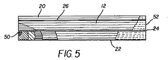
出願人は、OLEDディスプレイの内部と本発明のさまざまな実施態様の内部における熱流を分析するための多彩なモデルを開発した。図2に従来のOLEDディスプレイの熱モデルを示してある。このモデルは左縁部を中心として対称になっているため、この図と以下の図では右半分の最も左側の部分を図示してある。この構造では、ガラス基板22(厚さ700μm)をガラス・カバー12(やはり厚さ700μm)で封止する。基板22と封止用カバー12の間のギャップ24がこれら2つの要素を隔てている。エネルギーを加えると点50の温度が60℃まで上昇する。図2で同じ模様の領域は、温度がほぼ同じになっている範囲を表わす。図2に示した基板22とカバー12の最も右側にある等温範囲52の温度は29℃である。
Applicants have developed a variety of models for analyzing the heat flow within an OLED display and within various embodiments of the present invention. Figure 2 shows the thermal model of a conventional OLED display. Since this model is symmetrical about the left edge, the leftmost part of the right half is shown in this figure and the following figures. In this structure, a glass substrate 22 (thickness 700 μm) is sealed with a glass cover 12 (again, thickness 700 μm). A
図3には、本発明の一実施態様によるトップ・エミッション型OLEDディスプレイの熱モデルが示してある。この構造では、ガラス基板22(厚さ700μm)を封止用ガラス・カバー12(やはり厚さ700μm)で封止する。図2のモデルと同じ量のエネルギーをカバー12とガラス基板22の間にある点50に加える。基板22と熱伝導率が同じ熱伝導性接着剤26により、(熱伝導率が基板22の熱伝導率がよりも実質的に大きい)熱伝導性背面プレート20を基板22に接着させる。加えられたエネルギーによって点50の温度は40℃までしか上昇しない。図2におけるのと同様、図3で同じ模様の領域は、温度がほぼ同じになっている範囲を表わす。図2と図3を比較してわかるように、本発明のこの実施態様では、OLEDデバイスの点50における温度が有意に低い。熱伝導性背面プレートは、熱は散逸させないが、熱を加えた点50から熱を移動させ、基板22全体により均等に熱を分布させることで、点50における局所的な発熱を少なくする。
FIG. 3 shows a thermal model of a top emission OLED display according to an embodiment of the present invention. In this structure, a glass substrate 22 (thickness: 700 μm) is sealed with a sealing glass cover 12 (again, thickness: 700 μm). The same amount of energy as in the model of FIG. 2 is applied to the
図4aと図4bには、本発明の別の実施態様におけるボトム・エミッション型OLEDディスプレイの側面図が示してある。このOLEDディスプレイは、基板22と、基板上に形成された第1の電極30と、第1の電極30の上に位置する1つ以上のOLED発光層32と、OLED発光層32の上に位置する第2の電極34とを備える1つ以上のOLED発光素子、第2の電極34の上方に位置して基板22に固定されている封止用カバー12、熱伝導性接着剤26、及び熱伝導性接着剤26によって封止用カバー12に接着された実質的に平坦な熱伝導性背面プレート20を備えている。図4bに示した別の一実施態様では、実質的に平坦な熱伝導性背面プレート20が封止用カバー12の側部まで延びていて、OLEDディスプレイの縁部を保護している。熱伝導性接着剤26も封止用カバーの側部に沿って延びることで熱接触を改善することが好ましい。図4cに示してあるように、背面プレート20を基板22の側部に沿って延ばすこともできる。すると基板の側部が効果的に封止される。
4a and 4b show side views of a bottom emission OLED display in another embodiment of the present invention. The OLED display includes a
ボトム・エミッション型OLEDディスプレイもトップ・エミッション型と同様に作動するが、光がカバーではなく基板を通過するという違いがある。したがってボトム・エミッション型OLEDディスプレイの場合には、基板22が透明でなければならない一方で、封止用カバー12は不透明にすることができる。
Bottom-emission OLED displays operate in the same way as top-emissions, with the difference that light passes through the substrate instead of the cover. Therefore, in the case of a bottom emission type OLED display, the sealing
図5には、本発明の一実施態様によるボトム・エミッション型OLEDディスプレイの熱モデルが示してある。図2に示した従来モデルと同じ量のエネルギーを基板22の点50に加える。加えられたエネルギーによって点50の温度が43℃まで上昇する。図3におけるのと同様、同じ模様の領域は、温度がほぼ同じになっている範囲を表わす。熱伝導性背面プレートが熱を加えた点50から熱を移動させ、基板22全体により均等に熱を分布させることで、局所的な発熱を少なくしていることがわかる。図2、図3、図5を比較してわかるように、本発明の熱伝導性接着剤26と熱伝導性背面プレート20を用いると、OLEDデバイスの点50における温度が有意に低下する。
FIG. 5 shows a thermal model of a bottom emission OLED display according to an embodiment of the present invention. The same amount of energy as in the conventional model shown in FIG. The applied energy raises the temperature at
本発明に関して説明したように、両方の場合(図3と図5)において、基板22または封止用カバー12と熱接触させて接着した熱伝導性背面プレート20を用いることで、基板およびカバーの局所的な発熱と、これらと密に熱接触するように堆積させた発光材料の局所的な発熱が有意に低下する。発熱の低下は、発光材料の老化を減らす好ましい効果を有する。このモデル作成作業は、市販されている従来のモデル作成ツールを用いて実施する。
As described in connection with the present invention, in both cases (FIGS. 3 and 5), the use of a thermally
出願人は、この明細書に記載した熱伝導性接着剤と熱伝導性背面プレートを用いることにより、OLEDの作動に伴う発熱が減少することを実験的に証明した。この実験は、この明細書に記載したようにして材料をOLEDに付着させ、そのOLEDを熱から保護されたチェンバー内で作動させることによって行なった。熱イメージング・カメラと熱電対を使用し、OLEDデバイスのカバー、基板、熱伝導性背面プレートの温度をさまざまな作動条件下で測定した。熱伝導率が0.2W/mKよりも大きい(0.4W/mKよりも大きいことが好ましく、1.0W/mKよりも大きいことが最も好ましい)接着剤を用いると、熱伝導率が0.176W/mKである相対的に非熱伝導性である接着剤を用いた場合よりも局所的な発熱が減少した。最良の結果は、背面プレートを接着させた基板またはカバーと熱伝導率が少なくとも同じである熱伝導性接着剤を用いたときに得られた。 Applicants have experimentally demonstrated that using the thermally conductive adhesive and thermally conductive back plate described in this document reduces the heat generation associated with OLED operation. This experiment was performed by depositing material on the OLED as described herein and operating the OLED in a chamber protected from heat. Using thermal imaging cameras and thermocouples, the temperature of the OLED device cover, substrate, and thermally conductive back plate was measured under various operating conditions. With an adhesive with a thermal conductivity greater than 0.2 W / mK (preferably greater than 0.4 W / mK, most preferably greater than 1.0 W / mK), the thermal conductivity is 0.176 W / mK There was less local heat generation than with some relatively non-thermal conductive adhesive. The best results were obtained when using a thermally conductive adhesive that had at least the same thermal conductivity as the substrate or cover to which the back plate was bonded.
本発明では、集積回路で用いられている従来のヒートシンクとは異なり、フラット・パネル・ディスプレイの外面に接着されていてその外面全体に広がっているが、熱の散逸が主たる目的ではない実質的に平坦な背面プレートを使用する。このように実質的に平坦な背面プレートは、両面を平坦で滑らかにすることができる。あるいは望むのであれば、背面プレートの一方の面を波型にして表面積を大きくすることで、熱伝導性背面プレートが熱を環境に逃がす能力を増大させる。図6には、1つの面が波型になった熱伝導性背面プレート20が示してある。この場合には、熱伝導性背面プレート20の厚さが一定でない。波型表面により、熱伝導性背面プレート20から周囲環境への熱伝導を改善することができる。しかし好ましい実施態様によれば、実質的に平坦な背面プレートは、デバイスの全体的な厚さを最少にするため、図1と図4に示したように両面が平坦である。
In the present invention, unlike conventional heat sinks used in integrated circuits, it is bonded to the outer surface of the flat panel display and spreads over the entire outer surface, but the dissipation of heat is not the main purpose. Use a flat back plate. Thus, a substantially flat back plate can be flat and smooth on both sides. Alternatively, if desired, one surface of the back plate can be corrugated to increase the surface area, thereby increasing the ability of the thermally conductive back plate to release heat to the environment. FIG. 6 shows a thermally
基板22または封止用カバー12のサイズ、熱伝導性背面プレート20の厚さ、材料の相対的熱膨張係数(CTE)がどのような値であるかに応じ、基板/封止用カバーと熱伝導性背面プレートの間で熱に関係した膨張が適合しないという問題に遭遇する可能性がある。この問題は、面の間で移動できる熱伝導性接着剤を用いることによって改善できる。
Depending on the size of the
本発明によれば、基板22または封止用カバー12は、堅固でも可撓性があってもよい。さらに、これらと合わせて使用する熱伝導性背面プレートも可撓性のあるものにできる。金属またはガラスからなる適度に薄い層をカバーまたは基板で使用することができる。特に、可撓性のあるプラスチックを使用できる。可撓性のあるプラスチック材料だと環境中のガスまたは液体からOLEDディスプレイが効果的に保護されないため、熱伝導性背面プレート20にはOLEDディスプレイを環境から保護する追加保護部材を設けるとよい。環境に対する障壁層を有する可撓性プラスチック基板が提案されてきた。しかしこのような複合基板は、プラスチック基板の縁部から環境汚染物の侵入を相変わらず受けやすい。上に説明したように、本発明の熱伝導性背面プレートは、基板および/またはカバーの縁部も封止できるため、環境からもうまく保護することができる。
According to the present invention, the
熱は、熱伝導性背面プレート20と、例えばディスプレイの縁部で熱接触している従来のヒートシンクとを用いて本発明のOLEDディスプレイから除去することもできる。電気製品の内部で使用するとき、その電気製品を熱伝導性背面プレートと熱接触させて外部ヒートシンクにすることができる。
Heat can also be removed from the OLED display of the present invention using a thermally
(例えば金属でできている場合の)熱伝導性背面プレートは導電性にもなりうるため、OLEDディスプレイからの、またはOLEDディスプレイへの電磁放射を減らすのに用いることもできる。導電性背面プレートをグラウンドに接続することにより、ディスプレイからの、またはディスプレイの近くにある電気素子からの電磁干渉を減らすことができる。 A thermally conductive back plate (for example made of metal) can also be electrically conductive and can therefore be used to reduce electromagnetic radiation from or to the OLED display. By connecting the conductive back plate to ground, electromagnetic interference from the display or from electrical elements near the display can be reduced.
12 封止用カバー
20 熱伝導性背面プレート
22 基板
24 ギャップ
26 熱伝導性接着剤
30 第1の電極
32 OLED発光層
34 第2の電極
40 発光領域
50 エネルギー注入点
52 等温範囲
12 Sealing cover
20 Thermally conductive back plate
22 Board
24 gap
26 Thermally conductive adhesive
30 First electrode
32 OLED light emitting layer
34 Second electrode
40 Light emitting area
50 Energy injection point
52 Isothermal range
Claims (32)
b)該基板上に形成された第1の電極と、該第1の電極の上に位置する1つ以上のOLED発光層と、該OLED発光層の上に位置する第2の電極とを備える1つ以上のOLED発光素子と;
c)該第2の電極の上方に位置する封止用カバーと;
d)該封止用カバーまたは該基板の外面上に延在しそこに熱伝導性接着剤で接着された実質的に平坦な熱伝導性背面プレートとを含んでなり、該背面プレートの熱伝導率が該基板または該カバーの熱伝導率よりも大きく、かつ、該熱伝導性接着剤の熱伝導率が0.2W/mKよりも大きいことを特徴とするOLEDディスプレイ。 a) with a substrate;
b) comprising a first electrode formed on the substrate, one or more OLED light-emitting layers located on the first electrode, and a second electrode located on the OLED light-emitting layer One or more OLED light emitting elements;
c) a sealing cover located above the second electrode;
d) a substantially flat thermally conductive back plate extending over the sealing cover or the outer surface of the substrate and bonded thereto with a thermally conductive adhesive, the thermal conductivity of the back plate An OLED display, wherein the thermal conductivity of the substrate or the cover is greater than that of the substrate or the cover, and the thermal conductivity of the thermally conductive adhesive is greater than 0.2 W / mK.
b)該基板上に形成された第1の電極と、該第1の電極の上に位置する1つ以上のOLED発光層と、該OLED発光層の上に位置する第2の電極とを備える1つ以上のOLED発光素子と;
c)該第2の電極の上方に位置する封止用カバーと;
d)該封止用カバーまたは該基板の外面上に延在しそこに熱伝導性接着剤で接着された実質的に平坦な熱伝導性背面プレートとを含んでなり、該背面プレートの熱伝導率が該基板または該カバーの熱伝導率よりも大きく、かつ、該熱伝導性接着剤の熱伝導率が、該熱伝導性接着剤が付着する該カバーまたは該基板の熱伝導率以上であることを特徴とするOLEDディスプレイ。 a) with a substrate;
b) comprising a first electrode formed on the substrate, one or more OLED light-emitting layers located on the first electrode, and a second electrode located on the OLED light-emitting layer One or more OLED light emitting elements;
c) a sealing cover located above the second electrode;
d) a substantially flat thermally conductive back plate extending over the sealing cover or the outer surface of the substrate and bonded thereto with a thermally conductive adhesive, the thermal conductivity of the back plate The thermal conductivity of the substrate or the cover is greater than the thermal conductivity of the cover or the substrate to which the thermal conductive adhesive is attached. OLED display characterized by that.
Applications Claiming Priority (2)
| Application Number | Priority Date | Filing Date | Title |
|---|---|---|---|
| US10/785,825 US6967439B2 (en) | 2004-02-24 | 2004-02-24 | OLED display having thermally conductive backplate |
| PCT/US2005/005783 WO2005083666A2 (en) | 2004-02-24 | 2005-02-24 | Oled display having thermally conductive backplate |
Related Child Applications (1)
| Application Number | Title | Priority Date | Filing Date |
|---|---|---|---|
| JP2011149025A Division JP2011204692A (en) | 2004-02-24 | 2011-07-05 | Oled display having thermally conductive backplate |
Publications (2)
| Publication Number | Publication Date |
|---|---|
| JP2007525713A true JP2007525713A (en) | 2007-09-06 |
| JP2007525713A5 JP2007525713A5 (en) | 2008-03-21 |
Family
ID=34861692
Family Applications (2)
| Application Number | Title | Priority Date | Filing Date |
|---|---|---|---|
| JP2007500951A Pending JP2007525713A (en) | 2004-02-24 | 2005-02-24 | OLED display with thermally conductive back plate |
| JP2011149025A Pending JP2011204692A (en) | 2004-02-24 | 2011-07-05 | Oled display having thermally conductive backplate |
Family Applications After (1)
| Application Number | Title | Priority Date | Filing Date |
|---|---|---|---|
| JP2011149025A Pending JP2011204692A (en) | 2004-02-24 | 2011-07-05 | Oled display having thermally conductive backplate |
Country Status (6)
| Country | Link |
|---|---|
| US (1) | US6967439B2 (en) |
| EP (1) | EP1719194A2 (en) |
| JP (2) | JP2007525713A (en) |
| KR (1) | KR101094735B1 (en) |
| TW (1) | TWI360366B (en) |
| WO (1) | WO2005083666A2 (en) |
Cited By (17)
| Publication number | Priority date | Publication date | Assignee | Title |
|---|---|---|---|---|
| JP2009245770A (en) * | 2008-03-31 | 2009-10-22 | Sumitomo Chemical Co Ltd | Organic electroluminescent device |
| JP2010520588A (en) * | 2007-03-02 | 2010-06-10 | イーストマン コダック カンパニー | Flat panel OLED device with deformable substrate |
| JP2010520587A (en) * | 2007-03-02 | 2010-06-10 | イーストマン コダック カンパニー | Flat panel OLED device with deformable substrate |
| JP2010146894A (en) * | 2008-12-19 | 2010-07-01 | Sumitomo Chemical Co Ltd | Organic electroluminescence element |
| JP2011008937A (en) * | 2009-06-23 | 2011-01-13 | Seiko Epson Corp | Organic el device, and electronic apparatus |
| KR20110050985A (en) * | 2009-11-09 | 2011-05-17 | 엘지디스플레이 주식회사 | Organic electro-luminescence device |
| JP2011118082A (en) * | 2009-12-02 | 2011-06-16 | Seiko Epson Corp | Electrooptic device and electronic equipment |
| JP2011165489A (en) * | 2010-02-10 | 2011-08-25 | Lumiotec Kk | Organic el lighting system |
| JP2012212555A (en) * | 2011-03-31 | 2012-11-01 | Panasonic Corp | Light-emitting device |
| JP2013051046A (en) * | 2011-08-30 | 2013-03-14 | Panasonic Corp | Lighting device |
| JP2014534618A (en) * | 2011-09-30 | 2014-12-18 | アップル インコーポレイテッド | Built-in thermal diffusion |
| KR20160009176A (en) * | 2014-07-15 | 2016-01-26 | 삼성디스플레이 주식회사 | Organic light emitting display |
| JP2017103153A (en) * | 2015-12-03 | 2017-06-08 | コニカミノルタ株式会社 | Organic el module, optical writing device and image forming device |
| JP2018500731A (en) * | 2014-12-03 | 2018-01-11 | 深▲セン▼市華星光電技術有限公司 | Flexible OLED substrate and flexible OLED mounting method |
| KR20180033375A (en) * | 2016-09-23 | 2018-04-03 | 삼성디스플레이 주식회사 | Display device and manufacturing method thereof |
| JP2021076756A (en) * | 2019-11-12 | 2021-05-20 | 三菱電機株式会社 | Display unit and display device |
| WO2021210261A1 (en) * | 2020-04-15 | 2021-10-21 | 株式会社デンソー | Display device and method for manufacturing display device |
Families Citing this family (33)
| Publication number | Priority date | Publication date | Assignee | Title |
|---|---|---|---|---|
| DE10316933A1 (en) * | 2003-04-12 | 2004-10-21 | E+E Elektronik Gmbh | Sensor system and method for its production |
| US7329027B2 (en) * | 2004-10-29 | 2008-02-12 | Eastman Kodak Company | Heat conducting mounting fixture for solid-state lamp |
| US7692207B2 (en) * | 2005-01-21 | 2010-04-06 | Luminus Devices, Inc. | Packaging designs for LEDs |
| CA2605209C (en) * | 2005-04-19 | 2013-10-22 | Denki Kagaku Kogyo Kabushiki Kaisha | Metal base circuit board, light-emitting diode and led light source unit |
| US20070115686A1 (en) * | 2005-11-23 | 2007-05-24 | Luc Tyberghien | Lighting assembly, backlight assembly, display panel, and methods of temperature control |
| JP2007232802A (en) * | 2006-02-27 | 2007-09-13 | Hitachi Displays Ltd | Organic electroluminescence display device |
| JP4886540B2 (en) * | 2006-03-01 | 2012-02-29 | キヤノン株式会社 | Organic EL element panel |
| KR101307547B1 (en) * | 2006-11-27 | 2013-09-12 | 엘지디스플레이 주식회사 | Organic light emitting diodes display |
| EP2132778A1 (en) * | 2007-03-29 | 2009-12-16 | Koninklijke Philips Electronics N.V. | Light-emitting device comprising an elastomeric layer |
| KR100922357B1 (en) * | 2008-02-04 | 2009-10-21 | 삼성모바일디스플레이주식회사 | Organic light emitting display |
| DE102008031533B4 (en) * | 2008-07-03 | 2021-10-21 | Pictiva Displays International Limited | Organic electronic component |
| JP2010277781A (en) * | 2009-05-27 | 2010-12-09 | Toshiba Mobile Display Co Ltd | Organic el device |
| KR101267534B1 (en) * | 2009-10-30 | 2013-05-23 | 엘지디스플레이 주식회사 | methode of fabricating organic electro-luminescence device |
| WO2011096923A1 (en) * | 2010-02-03 | 2011-08-11 | Universal Display Corporation | Organic light emitting device with conducting cover |
| CN101866943B (en) * | 2010-02-26 | 2013-12-25 | 信利半导体有限公司 | Organic light-emitting diode display and packaging method thereof |
| DE102010014613A1 (en) * | 2010-04-09 | 2011-10-13 | Ledon Oled Lighting Gmbh & Co.Kg | Flat luminous body, arrangement of flat luminous bodies and method for producing flat luminous bodies |
| KR101890565B1 (en) * | 2011-02-14 | 2018-08-23 | 가부시키가이샤 한도오따이 에네루기 켄큐쇼 | Lighting device |
| EP2527910B1 (en) | 2011-05-24 | 2017-08-09 | Sony Corporation | Display |
| JP2013008016A (en) * | 2011-05-24 | 2013-01-10 | Sony Corp | Display unit |
| US8829556B2 (en) | 2011-09-01 | 2014-09-09 | General Electric Company | Thermal management in large area flexible OLED assembly |
| US20130070440A1 (en) * | 2011-09-21 | 2013-03-21 | Universal Display Corporation | OLED Light Panel in Combination with a Gobo |
| DE102012200485A1 (en) * | 2012-01-13 | 2013-07-18 | Osram Opto Semiconductors Gmbh | Organic light-emitting device and method for processing an organic light-emitting device |
| TWI514565B (en) * | 2013-12-16 | 2015-12-21 | Au Optronics Corp | Organic light emitting device and manufacturing method thereof |
| KR101696013B1 (en) * | 2013-12-26 | 2017-01-23 | 주식회사 포스코 | Panel for display apparatus |
| KR102439040B1 (en) * | 2014-12-01 | 2022-09-01 | 엘지디스플레이 주식회사 | Organic light emitting display device and rollable organic light emitting display system including the same |
| CN104538432B (en) * | 2015-01-05 | 2019-03-15 | 昆山工研院新型平板显示技术中心有限公司 | Display device |
| CN104701353A (en) * | 2015-03-27 | 2015-06-10 | 京东方科技集团股份有限公司 | Organic light-emitting display panel and display device |
| CN104821138B (en) * | 2015-05-21 | 2018-03-27 | 京东方科技集团股份有限公司 | A kind of flexible display panels open folding assist device and flexible display device |
| TWI635639B (en) * | 2017-01-05 | 2018-09-11 | 機光科技股份有限公司 | High refraction and high thermal conductivity OLED element |
| JP6944169B2 (en) * | 2017-04-25 | 2021-10-06 | 株式会社Nsc | Protective cover for display |
| KR102631248B1 (en) | 2019-07-17 | 2024-01-31 | 구글 엘엘씨 | Metal plate design for electronic display panels |
| CN111628110A (en) * | 2020-06-24 | 2020-09-04 | 京东方科技集团股份有限公司 | Display module and display device |
| CN114967234B (en) * | 2022-05-26 | 2023-11-03 | 京东方科技集团股份有限公司 | Display backboard, adjusting method thereof and display device |
Citations (8)
| Publication number | Priority date | Publication date | Assignee | Title |
|---|---|---|---|---|
| JPH08138578A (en) * | 1994-11-15 | 1996-05-31 | Canon Inc | Image forming device |
| JPH10275680A (en) * | 1997-03-31 | 1998-10-13 | Toyota Central Res & Dev Lab Inc | Organic el element |
| JP2001237063A (en) * | 2000-02-22 | 2001-08-31 | Seiko Epson Corp | Organic electroluminescent light source |
| JP2002208478A (en) * | 2000-12-23 | 2002-07-26 | Lg Philips Lcd Co Ltd | Electroluminescent element |
| JP2002343555A (en) * | 2001-05-18 | 2002-11-29 | Rohm Co Ltd | Organic el display device |
| JP2002343559A (en) * | 2001-05-18 | 2002-11-29 | Rohm Co Ltd | Organic el display device |
| JP2003075912A (en) * | 2001-09-06 | 2003-03-12 | Sony Corp | Liquid crystal projector and its assembling method |
| JP2005141194A (en) * | 2003-10-14 | 2005-06-02 | Seiko Epson Corp | Reinforcement structure, display device, and electronic equipment |
Family Cites Families (17)
| Publication number | Priority date | Publication date | Assignee | Title |
|---|---|---|---|---|
| JPS5880622A (en) * | 1981-11-09 | 1983-05-14 | Nec Corp | Liquid crystal display |
| JPH10275681A (en) * | 1997-03-31 | 1998-10-13 | Toyota Central Res & Dev Lab Inc | Organic el element |
| US6265820B1 (en) * | 1998-01-29 | 2001-07-24 | Emagin Corporation | Heat removal system for use in organic light emitting diode displays having high brightness |
| JP4066547B2 (en) * | 1999-01-25 | 2008-03-26 | 松下電器産業株式会社 | Display device |
| US6641933B1 (en) * | 1999-09-24 | 2003-11-04 | Semiconductor Energy Laboratory Co., Ltd. | Light-emitting EL display device |
| JP2001237062A (en) * | 2000-02-22 | 2001-08-31 | Seiko Epson Corp | Organic electroluminescent light source |
| JP2002194306A (en) * | 2000-12-26 | 2002-07-10 | Sekisui Chem Co Ltd | Heat-conductive sheet |
| JP2002278480A (en) * | 2001-03-15 | 2002-09-27 | Matsushita Electric Ind Co Ltd | Display panel device |
| JP3983120B2 (en) * | 2001-07-30 | 2007-09-26 | 富士通日立プラズマディスプレイ株式会社 | IC chip mounting structure and display device |
| JP2003059644A (en) * | 2001-08-09 | 2003-02-28 | Matsushita Electric Ind Co Ltd | Electroluminescent element |
| JP4019690B2 (en) * | 2001-11-02 | 2007-12-12 | セイコーエプソン株式会社 | ELECTRO-OPTICAL DEVICE, MANUFACTURING METHOD THEREOF, AND ELECTRONIC DEVICE |
| JP2003178876A (en) * | 2001-12-07 | 2003-06-27 | Sony Corp | Self-luminous display equipment |
| US6480389B1 (en) * | 2002-01-04 | 2002-11-12 | Opto Tech Corporation | Heat dissipation structure for solid-state light emitting device package |
| US6833671B2 (en) * | 2002-05-23 | 2004-12-21 | Kuan-Chang Peng | Organic electroluminescent device with efficient heat dissipation and method for manufacturing the same |
| TW577242B (en) * | 2002-08-19 | 2004-02-21 | Ritdisplay Corp | Organic light emitting panel and method of manufacturing the same |
| TW560703U (en) * | 2002-10-25 | 2003-11-01 | Ritdisplay Corp | Organic light-emitting diode |
| JP2005024961A (en) * | 2003-07-03 | 2005-01-27 | Seiko Epson Corp | Electrooptical device and electronic apparatus |
-
2004
- 2004-02-24 US US10/785,825 patent/US6967439B2/en not_active Expired - Lifetime
-
2005
- 2005-02-22 TW TW094105136A patent/TWI360366B/en active
- 2005-02-24 EP EP05723596A patent/EP1719194A2/en not_active Withdrawn
- 2005-02-24 JP JP2007500951A patent/JP2007525713A/en active Pending
- 2005-02-24 KR KR1020067016955A patent/KR101094735B1/en active IP Right Grant
- 2005-02-24 WO PCT/US2005/005783 patent/WO2005083666A2/en active Application Filing
-
2011
- 2011-07-05 JP JP2011149025A patent/JP2011204692A/en active Pending
Patent Citations (8)
| Publication number | Priority date | Publication date | Assignee | Title |
|---|---|---|---|---|
| JPH08138578A (en) * | 1994-11-15 | 1996-05-31 | Canon Inc | Image forming device |
| JPH10275680A (en) * | 1997-03-31 | 1998-10-13 | Toyota Central Res & Dev Lab Inc | Organic el element |
| JP2001237063A (en) * | 2000-02-22 | 2001-08-31 | Seiko Epson Corp | Organic electroluminescent light source |
| JP2002208478A (en) * | 2000-12-23 | 2002-07-26 | Lg Philips Lcd Co Ltd | Electroluminescent element |
| JP2002343555A (en) * | 2001-05-18 | 2002-11-29 | Rohm Co Ltd | Organic el display device |
| JP2002343559A (en) * | 2001-05-18 | 2002-11-29 | Rohm Co Ltd | Organic el display device |
| JP2003075912A (en) * | 2001-09-06 | 2003-03-12 | Sony Corp | Liquid crystal projector and its assembling method |
| JP2005141194A (en) * | 2003-10-14 | 2005-06-02 | Seiko Epson Corp | Reinforcement structure, display device, and electronic equipment |
Cited By (25)
| Publication number | Priority date | Publication date | Assignee | Title |
|---|---|---|---|---|
| JP2010520588A (en) * | 2007-03-02 | 2010-06-10 | イーストマン コダック カンパニー | Flat panel OLED device with deformable substrate |
| JP2010520587A (en) * | 2007-03-02 | 2010-06-10 | イーストマン コダック カンパニー | Flat panel OLED device with deformable substrate |
| JP2009245770A (en) * | 2008-03-31 | 2009-10-22 | Sumitomo Chemical Co Ltd | Organic electroluminescent device |
| JP2010146894A (en) * | 2008-12-19 | 2010-07-01 | Sumitomo Chemical Co Ltd | Organic electroluminescence element |
| JP2011008937A (en) * | 2009-06-23 | 2011-01-13 | Seiko Epson Corp | Organic el device, and electronic apparatus |
| KR101593059B1 (en) * | 2009-11-09 | 2016-02-11 | 엘지디스플레이 주식회사 | Organic electro-luminescence device |
| KR20110050985A (en) * | 2009-11-09 | 2011-05-17 | 엘지디스플레이 주식회사 | Organic electro-luminescence device |
| JP2011118082A (en) * | 2009-12-02 | 2011-06-16 | Seiko Epson Corp | Electrooptic device and electronic equipment |
| JP2011165489A (en) * | 2010-02-10 | 2011-08-25 | Lumiotec Kk | Organic el lighting system |
| JP2012212555A (en) * | 2011-03-31 | 2012-11-01 | Panasonic Corp | Light-emitting device |
| JP2013051046A (en) * | 2011-08-30 | 2013-03-14 | Panasonic Corp | Lighting device |
| JP2014534618A (en) * | 2011-09-30 | 2014-12-18 | アップル インコーポレイテッド | Built-in thermal diffusion |
| KR101606301B1 (en) | 2011-09-30 | 2016-03-24 | 애플 인크. | Integrated thermal spreading |
| KR102231946B1 (en) * | 2014-07-15 | 2021-03-26 | 삼성디스플레이 주식회사 | Organic light emitting display |
| KR20160009176A (en) * | 2014-07-15 | 2016-01-26 | 삼성디스플레이 주식회사 | Organic light emitting display |
| JP2018500731A (en) * | 2014-12-03 | 2018-01-11 | 深▲セン▼市華星光電技術有限公司 | Flexible OLED substrate and flexible OLED mounting method |
| JP2017103153A (en) * | 2015-12-03 | 2017-06-08 | コニカミノルタ株式会社 | Organic el module, optical writing device and image forming device |
| KR20180033375A (en) * | 2016-09-23 | 2018-04-03 | 삼성디스플레이 주식회사 | Display device and manufacturing method thereof |
| US12052909B2 (en) | 2016-09-23 | 2024-07-30 | Samsung Display Co., Ltd. | Display device and manufacturing method thereof |
| KR102694860B1 (en) * | 2016-09-23 | 2024-08-13 | 삼성디스플레이 주식회사 | Display device and manufacturing method thereof |
| JP2021076756A (en) * | 2019-11-12 | 2021-05-20 | 三菱電機株式会社 | Display unit and display device |
| JP7233354B2 (en) | 2019-11-12 | 2023-03-06 | 三菱電機株式会社 | Display unit manufacturing method and display device manufacturing method |
| WO2021210261A1 (en) * | 2020-04-15 | 2021-10-21 | 株式会社デンソー | Display device and method for manufacturing display device |
| JP2021170070A (en) * | 2020-04-15 | 2021-10-28 | 株式会社デンソー | Display device and manufacturing method of display device |
| JP7276234B2 (en) | 2020-04-15 | 2023-05-18 | 株式会社デンソー | DISPLAY DEVICE AND METHOD FOR MANUFACTURING DISPLAY DEVICE |
Also Published As
| Publication number | Publication date |
|---|---|
| JP2011204692A (en) | 2011-10-13 |
| KR20070020206A (en) | 2007-02-20 |
| EP1719194A2 (en) | 2006-11-08 |
| TW200603670A (en) | 2006-01-16 |
| TWI360366B (en) | 2012-03-11 |
| WO2005083666A2 (en) | 2005-09-09 |
| KR101094735B1 (en) | 2011-12-16 |
| WO2005083666A3 (en) | 2006-07-20 |
| US20050184662A1 (en) | 2005-08-25 |
| US6967439B2 (en) | 2005-11-22 |
Similar Documents
| Publication | Publication Date | Title |
|---|---|---|
| US6967439B2 (en) | OLED display having thermally conductive backplate | |
| US7205718B2 (en) | OLED display having thermally conductive adhesive | |
| JP4555339B2 (en) | OLED display with electrodes | |
| JP2008504653A (en) | OLED display with thermally conductive material | |
| US20050285518A1 (en) | OLED display having thick cathode | |
| JP6189298B2 (en) | Temperature management in large area flexible OLED assemblies | |
| EP1693908B1 (en) | Organic electroluminescence display and method for manufacturing the same | |
| JP6105911B2 (en) | OLED display panel | |
| KR101084230B1 (en) | Organic light emitting diode display and method for manufacturing the same | |
| US7049745B2 (en) | OLED display having thermally conductive layer | |
| TW201944133A (en) | Heat dissipating structure, electronic device and display device using same | |
| KR101593059B1 (en) | Organic electro-luminescence device | |
| US20040085019A1 (en) | Organic light-emitting diode | |
| CN108417544A (en) | Heat dissipation element, using the production method of its electronic device and electronic device | |
| KR20060106225A (en) | Organic light emitting diodes | |
| JP2003100447A (en) | Organic electroluminescence equipment | |
| TWI227095B (en) | Organic light emitting diode (OLED) display and fabrication method thereof | |
| KR100680805B1 (en) | Organic Light Emitting Diodes | |
| KR100837638B1 (en) | Display Device | |
| JP2011187217A (en) | Organic el module | |
| KR100658346B1 (en) | Display Pannel with Organic Light Emitting Diodes |
Legal Events
| Date | Code | Title | Description |
|---|---|---|---|
| A521 | Request for written amendment filed |
Free format text: JAPANESE INTERMEDIATE CODE: A523 Effective date: 20080129 |
|
| A621 | Written request for application examination |
Free format text: JAPANESE INTERMEDIATE CODE: A621 Effective date: 20080129 |
|
| A977 | Report on retrieval |
Free format text: JAPANESE INTERMEDIATE CODE: A971007 Effective date: 20100428 |
|
| A131 | Notification of reasons for refusal |
Free format text: JAPANESE INTERMEDIATE CODE: A131 Effective date: 20100511 |
|
| A601 | Written request for extension of time |
Free format text: JAPANESE INTERMEDIATE CODE: A601 Effective date: 20100708 |
|
| A602 | Written permission of extension of time |
Free format text: JAPANESE INTERMEDIATE CODE: A602 Effective date: 20100715 |
|
| A711 | Notification of change in applicant |
Free format text: JAPANESE INTERMEDIATE CODE: A711 Effective date: 20100804 |
|
| A521 | Request for written amendment filed |
Free format text: JAPANESE INTERMEDIATE CODE: A523 Effective date: 20101110 |
|
| A131 | Notification of reasons for refusal |
Free format text: JAPANESE INTERMEDIATE CODE: A131 Effective date: 20110405 |
|
| A02 | Decision of refusal |
Free format text: JAPANESE INTERMEDIATE CODE: A02 Effective date: 20110913 |