JP2007515079A - Manufacturing method of super-junction device with conventional terminal - Google Patents
Manufacturing method of super-junction device with conventional terminal Download PDFInfo
- Publication number
- JP2007515079A JP2007515079A JP2006545755A JP2006545755A JP2007515079A JP 2007515079 A JP2007515079 A JP 2007515079A JP 2006545755 A JP2006545755 A JP 2006545755A JP 2006545755 A JP2006545755 A JP 2006545755A JP 2007515079 A JP2007515079 A JP 2007515079A
- Authority
- JP
- Japan
- Prior art keywords
- region
- grooves
- doped region
- conductivity type
- manufacturing
- Prior art date
- Legal status (The legal status is an assumption and is not a legal conclusion. Google has not performed a legal analysis and makes no representation as to the accuracy of the status listed.)
- Pending
Links
- 238000004519 manufacturing process Methods 0.000 title claims abstract description 28
- 239000004065 semiconductor Substances 0.000 claims abstract description 58
- 238000000034 method Methods 0.000 claims abstract description 27
- 239000002019 doping agent Substances 0.000 claims abstract description 21
- 239000000758 substrate Substances 0.000 claims abstract description 20
- 238000005530 etching Methods 0.000 claims abstract description 16
- 230000001681 protective effect Effects 0.000 claims abstract description 10
- 239000011810 insulating material Substances 0.000 claims abstract description 6
- 229920002120 photoresistant polymer Polymers 0.000 claims description 37
- 238000005468 ion implantation Methods 0.000 claims description 29
- 150000002500 ions Chemical class 0.000 claims description 18
- 238000002513 implantation Methods 0.000 claims description 16
- 238000000151 deposition Methods 0.000 claims description 13
- 230000008021 deposition Effects 0.000 claims description 8
- 238000009792 diffusion process Methods 0.000 claims description 6
- 239000000376 reactant Substances 0.000 claims description 3
- 238000010894 electron beam technology Methods 0.000 claims description 2
- 230000002265 prevention Effects 0.000 claims 1
- 230000015556 catabolic process Effects 0.000 description 5
- 239000004020 conductor Substances 0.000 description 3
- 230000015572 biosynthetic process Effects 0.000 description 2
- 238000005229 chemical vapour deposition Methods 0.000 description 2
- 230000006866 deterioration Effects 0.000 description 2
- 230000000694 effects Effects 0.000 description 2
- 239000012535 impurity Substances 0.000 description 2
- 230000000873 masking effect Effects 0.000 description 2
- 150000004706 metal oxides Chemical class 0.000 description 2
- 238000004140 cleaning Methods 0.000 description 1
- 238000005520 cutting process Methods 0.000 description 1
- 238000005137 deposition process Methods 0.000 description 1
- 238000001312 dry etching Methods 0.000 description 1
- 230000005669 field effect Effects 0.000 description 1
- 238000005429 filling process Methods 0.000 description 1
- 238000005304 joining Methods 0.000 description 1
- 229910044991 metal oxide Inorganic materials 0.000 description 1
- 230000001590 oxidative effect Effects 0.000 description 1
- 230000003071 parasitic effect Effects 0.000 description 1
- 238000002161 passivation Methods 0.000 description 1
Images


Classifications
-
- H—ELECTRICITY
- H01—ELECTRIC ELEMENTS
- H01L—SEMICONDUCTOR DEVICES NOT COVERED BY CLASS H10
- H01L29/00—Semiconductor devices adapted for rectifying, amplifying, oscillating or switching, or capacitors or resistors with at least one potential-jump barrier or surface barrier, e.g. PN junction depletion layer or carrier concentration layer; Details of semiconductor bodies or of electrodes thereof ; Multistep manufacturing processes therefor
- H01L29/66—Types of semiconductor device ; Multistep manufacturing processes therefor
- H01L29/68—Types of semiconductor device ; Multistep manufacturing processes therefor controllable by only the electric current supplied, or only the electric potential applied, to an electrode which does not carry the current to be rectified, amplified or switched
- H01L29/76—Unipolar devices, e.g. field effect transistors
- H01L29/772—Field effect transistors
- H01L29/78—Field effect transistors with field effect produced by an insulated gate
- H01L29/7801—DMOS transistors, i.e. MISFETs with a channel accommodating body or base region adjoining a drain drift region
- H01L29/7802—Vertical DMOS transistors, i.e. VDMOS transistors
- H01L29/7811—Vertical DMOS transistors, i.e. VDMOS transistors with an edge termination structure
-
- H—ELECTRICITY
- H01—ELECTRIC ELEMENTS
- H01L—SEMICONDUCTOR DEVICES NOT COVERED BY CLASS H10
- H01L21/00—Processes or apparatus adapted for the manufacture or treatment of semiconductor or solid state devices or of parts thereof
- H01L21/70—Manufacture or treatment of devices consisting of a plurality of solid state components formed in or on a common substrate or of parts thereof; Manufacture of integrated circuit devices or of parts thereof
- H01L21/77—Manufacture or treatment of devices consisting of a plurality of solid state components or integrated circuits formed in, or on, a common substrate
- H01L21/78—Manufacture or treatment of devices consisting of a plurality of solid state components or integrated circuits formed in, or on, a common substrate with subsequent division of the substrate into plural individual devices
- H01L21/82—Manufacture or treatment of devices consisting of a plurality of solid state components or integrated circuits formed in, or on, a common substrate with subsequent division of the substrate into plural individual devices to produce devices, e.g. integrated circuits, each consisting of a plurality of components
- H01L21/822—Manufacture or treatment of devices consisting of a plurality of solid state components or integrated circuits formed in, or on, a common substrate with subsequent division of the substrate into plural individual devices to produce devices, e.g. integrated circuits, each consisting of a plurality of components the substrate being a semiconductor, using silicon technology
- H01L21/8232—Field-effect technology
- H01L21/8234—MIS technology, i.e. integration processes of field effect transistors of the conductor-insulator-semiconductor type
- H01L21/823487—MIS technology, i.e. integration processes of field effect transistors of the conductor-insulator-semiconductor type with a particular manufacturing method of vertical transistor structures, i.e. with channel vertical to the substrate surface
-
- H—ELECTRICITY
- H01—ELECTRIC ELEMENTS
- H01L—SEMICONDUCTOR DEVICES NOT COVERED BY CLASS H10
- H01L29/00—Semiconductor devices adapted for rectifying, amplifying, oscillating or switching, or capacitors or resistors with at least one potential-jump barrier or surface barrier, e.g. PN junction depletion layer or carrier concentration layer; Details of semiconductor bodies or of electrodes thereof ; Multistep manufacturing processes therefor
- H01L29/02—Semiconductor bodies ; Multistep manufacturing processes therefor
- H01L29/06—Semiconductor bodies ; Multistep manufacturing processes therefor characterised by their shape; characterised by the shapes, relative sizes, or dispositions of the semiconductor regions ; characterised by the concentration or distribution of impurities within semiconductor regions
- H01L29/0603—Semiconductor bodies ; Multistep manufacturing processes therefor characterised by their shape; characterised by the shapes, relative sizes, or dispositions of the semiconductor regions ; characterised by the concentration or distribution of impurities within semiconductor regions characterised by particular constructional design considerations, e.g. for preventing surface leakage, for controlling electric field concentration or for internal isolations regions
- H01L29/0607—Semiconductor bodies ; Multistep manufacturing processes therefor characterised by their shape; characterised by the shapes, relative sizes, or dispositions of the semiconductor regions ; characterised by the concentration or distribution of impurities within semiconductor regions characterised by particular constructional design considerations, e.g. for preventing surface leakage, for controlling electric field concentration or for internal isolations regions for preventing surface leakage or controlling electric field concentration
- H01L29/0611—Semiconductor bodies ; Multistep manufacturing processes therefor characterised by their shape; characterised by the shapes, relative sizes, or dispositions of the semiconductor regions ; characterised by the concentration or distribution of impurities within semiconductor regions characterised by particular constructional design considerations, e.g. for preventing surface leakage, for controlling electric field concentration or for internal isolations regions for preventing surface leakage or controlling electric field concentration for increasing or controlling the breakdown voltage of reverse biased devices
- H01L29/0615—Semiconductor bodies ; Multistep manufacturing processes therefor characterised by their shape; characterised by the shapes, relative sizes, or dispositions of the semiconductor regions ; characterised by the concentration or distribution of impurities within semiconductor regions characterised by particular constructional design considerations, e.g. for preventing surface leakage, for controlling electric field concentration or for internal isolations regions for preventing surface leakage or controlling electric field concentration for increasing or controlling the breakdown voltage of reverse biased devices by the doping profile or the shape or the arrangement of the PN junction, or with supplementary regions, e.g. junction termination extension [JTE]
- H01L29/063—Reduced surface field [RESURF] pn-junction structures
- H01L29/0634—Multiple reduced surface field (multi-RESURF) structures, e.g. double RESURF, charge compensation, cool, superjunction (SJ), 3D-RESURF, composite buffer (CB) structures
-
- H—ELECTRICITY
- H01—ELECTRIC ELEMENTS
- H01L—SEMICONDUCTOR DEVICES NOT COVERED BY CLASS H10
- H01L29/00—Semiconductor devices adapted for rectifying, amplifying, oscillating or switching, or capacitors or resistors with at least one potential-jump barrier or surface barrier, e.g. PN junction depletion layer or carrier concentration layer; Details of semiconductor bodies or of electrodes thereof ; Multistep manufacturing processes therefor
- H01L29/02—Semiconductor bodies ; Multistep manufacturing processes therefor
- H01L29/06—Semiconductor bodies ; Multistep manufacturing processes therefor characterised by their shape; characterised by the shapes, relative sizes, or dispositions of the semiconductor regions ; characterised by the concentration or distribution of impurities within semiconductor regions
- H01L29/0603—Semiconductor bodies ; Multistep manufacturing processes therefor characterised by their shape; characterised by the shapes, relative sizes, or dispositions of the semiconductor regions ; characterised by the concentration or distribution of impurities within semiconductor regions characterised by particular constructional design considerations, e.g. for preventing surface leakage, for controlling electric field concentration or for internal isolations regions
- H01L29/0642—Isolation within the component, i.e. internal isolation
- H01L29/0649—Dielectric regions, e.g. SiO2 regions, air gaps
- H01L29/0653—Dielectric regions, e.g. SiO2 regions, air gaps adjoining the input or output region of a field-effect device, e.g. the source or drain region
-
- H—ELECTRICITY
- H01—ELECTRIC ELEMENTS
- H01L—SEMICONDUCTOR DEVICES NOT COVERED BY CLASS H10
- H01L29/00—Semiconductor devices adapted for rectifying, amplifying, oscillating or switching, or capacitors or resistors with at least one potential-jump barrier or surface barrier, e.g. PN junction depletion layer or carrier concentration layer; Details of semiconductor bodies or of electrodes thereof ; Multistep manufacturing processes therefor
- H01L29/02—Semiconductor bodies ; Multistep manufacturing processes therefor
- H01L29/06—Semiconductor bodies ; Multistep manufacturing processes therefor characterised by their shape; characterised by the shapes, relative sizes, or dispositions of the semiconductor regions ; characterised by the concentration or distribution of impurities within semiconductor regions
- H01L29/10—Semiconductor bodies ; Multistep manufacturing processes therefor characterised by their shape; characterised by the shapes, relative sizes, or dispositions of the semiconductor regions ; characterised by the concentration or distribution of impurities within semiconductor regions with semiconductor regions connected to an electrode not carrying current to be rectified, amplified or switched and such electrode being part of a semiconductor device which comprises three or more electrodes
- H01L29/1025—Channel region of field-effect devices
- H01L29/1029—Channel region of field-effect devices of field-effect transistors
- H01L29/1033—Channel region of field-effect devices of field-effect transistors with insulated gate, e.g. characterised by the length, the width, the geometric contour or the doping structure
- H01L29/1041—Channel region of field-effect devices of field-effect transistors with insulated gate, e.g. characterised by the length, the width, the geometric contour or the doping structure with a non-uniform doping structure in the channel region surface
- H01L29/1045—Channel region of field-effect devices of field-effect transistors with insulated gate, e.g. characterised by the length, the width, the geometric contour or the doping structure with a non-uniform doping structure in the channel region surface the doping structure being parallel to the channel length, e.g. DMOS like
-
- H—ELECTRICITY
- H01—ELECTRIC ELEMENTS
- H01L—SEMICONDUCTOR DEVICES NOT COVERED BY CLASS H10
- H01L29/00—Semiconductor devices adapted for rectifying, amplifying, oscillating or switching, or capacitors or resistors with at least one potential-jump barrier or surface barrier, e.g. PN junction depletion layer or carrier concentration layer; Details of semiconductor bodies or of electrodes thereof ; Multistep manufacturing processes therefor
- H01L29/66—Types of semiconductor device ; Multistep manufacturing processes therefor
- H01L29/66007—Multistep manufacturing processes
- H01L29/66075—Multistep manufacturing processes of devices having semiconductor bodies comprising group 14 or group 13/15 materials
- H01L29/66227—Multistep manufacturing processes of devices having semiconductor bodies comprising group 14 or group 13/15 materials the devices being controllable only by the electric current supplied or the electric potential applied, to an electrode which does not carry the current to be rectified, amplified or switched, e.g. three-terminal devices
- H01L29/66409—Unipolar field-effect transistors
- H01L29/66477—Unipolar field-effect transistors with an insulated gate, i.e. MISFET
- H01L29/66674—DMOS transistors, i.e. MISFETs with a channel accommodating body or base region adjoining a drain drift region
- H01L29/66712—Vertical DMOS transistors, i.e. VDMOS transistors
-
- H—ELECTRICITY
- H01—ELECTRIC ELEMENTS
- H01L—SEMICONDUCTOR DEVICES NOT COVERED BY CLASS H10
- H01L29/00—Semiconductor devices adapted for rectifying, amplifying, oscillating or switching, or capacitors or resistors with at least one potential-jump barrier or surface barrier, e.g. PN junction depletion layer or carrier concentration layer; Details of semiconductor bodies or of electrodes thereof ; Multistep manufacturing processes therefor
- H01L29/66—Types of semiconductor device ; Multistep manufacturing processes therefor
- H01L29/68—Types of semiconductor device ; Multistep manufacturing processes therefor controllable by only the electric current supplied, or only the electric potential applied, to an electrode which does not carry the current to be rectified, amplified or switched
- H01L29/76—Unipolar devices, e.g. field effect transistors
- H01L29/772—Field effect transistors
- H01L29/78—Field effect transistors with field effect produced by an insulated gate
- H01L29/7801—DMOS transistors, i.e. MISFETs with a channel accommodating body or base region adjoining a drain drift region
- H01L29/7802—Vertical DMOS transistors, i.e. VDMOS transistors
-
- H—ELECTRICITY
- H01—ELECTRIC ELEMENTS
- H01L—SEMICONDUCTOR DEVICES NOT COVERED BY CLASS H10
- H01L21/00—Processes or apparatus adapted for the manufacture or treatment of semiconductor or solid state devices or of parts thereof
- H01L21/02—Manufacture or treatment of semiconductor devices or of parts thereof
- H01L21/04—Manufacture or treatment of semiconductor devices or of parts thereof the devices having at least one potential-jump barrier or surface barrier, e.g. PN junction, depletion layer or carrier concentration layer
- H01L21/18—Manufacture or treatment of semiconductor devices or of parts thereof the devices having at least one potential-jump barrier or surface barrier, e.g. PN junction, depletion layer or carrier concentration layer the devices having semiconductor bodies comprising elements of Group IV of the Periodic System or AIIIBV compounds with or without impurities, e.g. doping materials
- H01L21/26—Bombardment with radiation
- H01L21/263—Bombardment with radiation with high-energy radiation
- H01L21/265—Bombardment with radiation with high-energy radiation producing ion implantation
- H01L21/26586—Bombardment with radiation with high-energy radiation producing ion implantation characterised by the angle between the ion beam and the crystal planes or the main crystal surface
-
- H—ELECTRICITY
- H01—ELECTRIC ELEMENTS
- H01L—SEMICONDUCTOR DEVICES NOT COVERED BY CLASS H10
- H01L21/00—Processes or apparatus adapted for the manufacture or treatment of semiconductor or solid state devices or of parts thereof
- H01L21/02—Manufacture or treatment of semiconductor devices or of parts thereof
- H01L21/04—Manufacture or treatment of semiconductor devices or of parts thereof the devices having at least one potential-jump barrier or surface barrier, e.g. PN junction, depletion layer or carrier concentration layer
- H01L21/18—Manufacture or treatment of semiconductor devices or of parts thereof the devices having at least one potential-jump barrier or surface barrier, e.g. PN junction, depletion layer or carrier concentration layer the devices having semiconductor bodies comprising elements of Group IV of the Periodic System or AIIIBV compounds with or without impurities, e.g. doping materials
- H01L21/26—Bombardment with radiation
- H01L21/263—Bombardment with radiation with high-energy radiation
- H01L21/265—Bombardment with radiation with high-energy radiation producing ion implantation
- H01L21/266—Bombardment with radiation with high-energy radiation producing ion implantation using masks
-
- H—ELECTRICITY
- H01—ELECTRIC ELEMENTS
- H01L—SEMICONDUCTOR DEVICES NOT COVERED BY CLASS H10
- H01L2924/00—Indexing scheme for arrangements or methods for connecting or disconnecting semiconductor or solid-state bodies as covered by H01L24/00
- H01L2924/0001—Technical content checked by a classifier
- H01L2924/0002—Not covered by any one of groups H01L24/00, H01L24/00 and H01L2224/00
Abstract
半導体ディバイスの製造方法は、強くドープされた第1導電率形の第1領域と、軽くドープされた第2導電率形の第2領域とを含む。半導体基板には複数個の溝が、その作動領域にエッチングされて形成され、複数個のメサを形成する。、作動領域の所定領域が酸化され、乾式酸化物エッチング法を用いてエッチングされて溝の酸化物を除去する。保護シールドが所定領域上から部分的に除去される。ドーパントが所定領域のメサに或る角度で打込まれる。複数個の溝は絶縁材料を備え、構造体の頂面が平坦化されて、この構造体に超接合装置が形成される。
【選択図】 なしA method of manufacturing a semiconductor device includes a first region of a first conductivity type that is heavily doped and a second region of a second conductivity type that is lightly doped. In the semiconductor substrate, a plurality of grooves are formed by etching in the operation region to form a plurality of mesas. A predetermined region of the working region is oxidized and etched using a dry oxide etching method to remove the oxide in the trench. The protective shield is partially removed from the predetermined area. The dopant is implanted into the mesa in a predetermined area at an angle. The plurality of grooves are provided with an insulating material, and the top surface of the structure is flattened to form a super junction device in the structure.
[Selection figure] None
Description
本発明は、作動領域の最後の溝の、イオンが打込まれていない外側壁を含む縁部端子構造体を備えた半導体ディバイスの製造方法、特に、作動中の抵抗が低く破壊電圧の高い、電力スイッチングに適した金属酸化物(MOS)ゲート半導体である半導体ディバイスに関するものである。 The invention relates to a method of manufacturing a semiconductor device with an edge terminal structure comprising an outer wall of the last groove of the active region that is not implanted with ions, in particular a low resistance during operation and a high breakdown voltage. The present invention relates to a semiconductor device which is a metal oxide (MOS) gate semiconductor suitable for power switching.
米国特許第5,216,275号に開示されている、キシンビ チェン博士(Dr. Xingbi Chen)による超接合装置の発明以来、彼の発明の超接合効果を拡大及び改良する多くの試みがなされた。米国特許第6,410,958号および米国特許第6,300,171号ならびに米国特許第6,307,246号はそのような努力の例であり、これらを言及することによりそれらの内容を本願に組み込むこととする。 Since the invention of the superjunction device by Dr. Xingbi Chen, disclosed in US Pat. No. 5,216,275, many attempts have been made to expand and improve the superjunction effect of his invention. . US Pat. No. 6,410,958 and US Pat. No. 6,300,171 and US Pat. No. 6,307,246 are examples of such efforts, the contents of which are hereby incorporated by reference. It will be incorporated into.
米国特許第6,410,958号(Usui, et al.)は縁部端子構造と半導体構成要素としてのドリフト領域に関する。1つの導電率形の半導体本体は、他の導電率形の複数個の領域が2つ以上の異なる面に埋め込まれている縁領域を有する。半導体構成要素の作動領域の下方に、その下にある基板を用いてドリフト領域が結合されている。 US Pat. No. 6,410,958 (Usui, et al.) Relates to edge terminal structures and drift regions as semiconductor components. A semiconductor body of one conductivity type has an edge region in which a plurality of regions of another conductivity type are embedded in two or more different surfaces. A drift region is coupled below the working region of the semiconductor component using the underlying substrate.
米国特許第6,307,246号(Nitta, et al.)は高電圧維持縁部構造体を有する半導体構成要素を開示する。この構造体内では、多数の平行に結合した個別の構成要素がセル通路の多数のセルに配置されている。縁領域では、半導体構成要素は、遮光源ゾーン領域を備えたセルを有する。この遮光源ゾーン領域では電力半導体構成要素の整流中、不均一に大きい逆電流密度によって寄生バイポーラートランジスタの電源が入るのを抑制する。更に、遮光源ゾーン領域を有する縁部構造体は、Nitta, et al.で論じられている科学技術条件で非常に簡単に製造できる。Nitta, et al.はパラメータの効果を明確にし、on状態で導電し、off状態では、導電しない平行PN層からなるドリフト層を有する超接合半導体ディバイスの大量生産を可能にしている。N形のドリフト領域での作動不純物の総量は、P形の区分領域の作動不純物の総量の100%から150%の範囲内である。加えて、N形ドリフト領域とP形区分領域とのいずれか一方の幅は、他方の領域の94%から106%の範囲内である。 US Pat. No. 6,307,246 (Nitta, et al.) Discloses a semiconductor component having a high voltage sustaining edge structure. Within this structure, a number of parallel coupled individual components are arranged in a number of cells of the cell passage. In the edge region, the semiconductor component has a cell with a shading source zone region. In this shading source zone region, during the rectification of the power semiconductor components, the parasitic bipolar transistor is prevented from being turned on by an unevenly large reverse current density. Furthermore, an edge structure with a shading source zone region can be manufactured very easily with the technological conditions discussed in Nitta, et al. Nitta, et al. Clarifies the effect of the parameters, enabling mass production of superjunction semiconductor devices having a drift layer consisting of parallel PN layers that conduct in the on state and in the off state. The total amount of working impurities in the N-type drift region is in the range of 100% to 150% of the total amount of working impurities in the P-type segmented region. In addition, the width of one of the N-type drift region and the P-type segmented region is in the range of 94% to 106% of the other region.
米国特許第6,300,171号(Frisina)は、高電圧半導体ディバイスの縁部構造体の製造方法を開示する。この方法は、第1導電率形の第1半導体層を形成する第1工程と、この第1半導体層の頂面上に第1マスクを形成する第2工程と、このマスクの一部を除去して、マスクに少なくとも1つの開口部を形成する第3工程と、この少なくとも1つの開口部を介して、第1半導体層に第2導電率形のドーパントを導入する第4工程と、第1マスクを完全に除去し、第1半導体層上に、第1導電率形の第2半導体層を形成する第5工程と、第1半導体層に打込んだドーパントを拡散させて、第1および第2の半導体層に第2導電率形のドープされた領域を形成する第6工程とを含む。第2工程から第6工程までを1回以上繰り返し、多数の第1導電率形の積層された半導体層と、第2導電率形の2列以上のドープ領域を含む最終縁部構造体を形成する。上記の列は、上記の多数の積層された半導体層に挿入され、その後マスクの開口部を介して打込まれたドープ領域を積層することにより形成され、高電圧半導体ディバイスに近い列は、それより遠い列よりも深い。 US Pat. No. 6,300,171 (Frisina) discloses a method of manufacturing an edge structure of a high voltage semiconductor device. The method includes a first step of forming a first semiconductor layer of a first conductivity type, a second step of forming a first mask on the top surface of the first semiconductor layer, and removing a part of the mask. A third step of forming at least one opening in the mask; a fourth step of introducing a dopant of the second conductivity type into the first semiconductor layer through the at least one opening; The mask is completely removed, a fifth step of forming a second semiconductor layer of the first conductivity type on the first semiconductor layer, and a dopant implanted into the first semiconductor layer are diffused, so that the first and first Forming a doped region of the second conductivity type in the second semiconductor layer. Repeat the second to sixth steps one or more times to form a final edge structure that includes a number of stacked semiconductor layers of the first conductivity type and two or more rows of doped regions of the second conductivity type. To do. The column is formed by stacking doped regions that are inserted into the multiple stacked semiconductor layers and then implanted through the openings in the mask, and the column close to the high voltage semiconductor device is Deeper than the farther columns.
半導体ディバイスの製造のため、唯一のエピタキシアル沈着工程を使用する方法に匹敵する技術を用いて製造される、イオンが打込まれていない、作動領域の最後の溝の外側壁を備えた縁部端子領域を提供することが望ましい。
簡単に述べると、本発明は、相互に対向する第1及び第2の主表面を有する半導体基板を設けることを含む半導体ディバイスの製造方法からなる。上記の半導体基板は、第2主表面に第1導電率形の強くドープされた領域を有し、第1主表面に第1導電率形の軽くドープされた領域を有する。この方法は、上記の半導体基板において、その作動領域に複数個の溝と複数個の台地(メサ)とをエッチングして設けることを含む。各溝は、強くドープされた領域に向け、第1主表面から第1深さ位置まで伸びる第1延長部分を有し、各メサは、第1主表面に対し所定の傾斜を維持する側壁面を有する。上記の複数個の溝の各々は、複数個のメサの1つにより、その他の溝の各々から離れている。この方法は、作動領域と、作動領域の外側およびこれに隣接する端子領域内に伸びる、複数個のメサと複数個の溝との所定領域を、各メサの頂部、複数個の溝の各々の両側壁面および底部ならびに端子領域の頂部を酸化物が覆うまで酸化することを含む。この方法は、複数個のメサと複数個の溝との所定領域を、乾式酸化物エンチング法によってエッチングし、複数個の溝の底部にある酸化物を除去することを含む。この方法は、作動領域と端子領域との間の境界の所定領域上に保護シールドを形成し、その後複数個のメサと複数個の溝との所定領域の上から保護シールドを部分的に除去することを含む。この方法は、複数個のメサと複数個の溝との所定領域の少なくとも1つのメサに、隣接対の溝において、1つの溝の側壁面で、第1導電率形のドーパントを、第1所定打込み角度で打込み、上記の1つの溝の側壁面に、強くドープされた領域より低いドープ濃度を有する第1導電率形の第1ドープ領域を形成することを含む。また、この方法は、複数個のメサと複数個の溝との上記所定の少なくとも1つののメサに、第1導電率形のドーパントを打込んだ側壁に対向する上記少なくとも1つのメサの側壁面で、第2導電率形のドーパントを、第2所定打込み角度で打込んで、第1導電率形のドーパントを打込んだ側壁に対向する側壁面に第2導電率形の第2ドープ領域を設けて、複数個の溝の少なくとも1つの溝の深さ方向に沿って位置する第1および第2ドープ領域のP−N接合を形成すると共に、作動領域の、イオンが打込まれていない外側壁を設けることを含む。この方法は、複数個の溝に絶縁材料を充填し、構造体の頂面を平坦化して、超接合装置をこの構造体上に形成することを含む。 Briefly stated, the present invention comprises a method of manufacturing a semiconductor device that includes providing a semiconductor substrate having first and second major surfaces opposite to each other. The semiconductor substrate has a strongly doped region of the first conductivity type on the second main surface and a lightly doped region of the first conductivity type on the first main surface. This method includes etching a plurality of grooves and a plurality of plates (mesas) in the operation region of the semiconductor substrate. Each groove has a first extension extending from the first main surface to a first depth position toward the heavily doped region, and each mesa has a sidewall surface that maintains a predetermined inclination with respect to the first main surface. Have Each of the plurality of grooves is separated from each of the other grooves by one of the plurality of mesas. In this method, a predetermined region of a plurality of mesas and a plurality of grooves extending outside the operation region and the terminal region adjacent to the operation region is formed on the top of each mesa and each of the plurality of grooves. Oxidizing until the oxide covers the side walls and bottom and the top of the terminal area. The method includes etching a predetermined region of the plurality of mesas and the plurality of grooves by a dry oxide etching method to remove the oxide at the bottom of the plurality of grooves. This method forms a protective shield on a predetermined region at the boundary between the operating region and the terminal region, and then partially removes the protective shield from the predetermined region of the plurality of mesas and the plurality of grooves. Including that. In this method, at least one mesa in a predetermined region of a plurality of mesas and a plurality of grooves is coated with a first conductivity type dopant on a side wall surface of one groove in a pair of adjacent grooves. Implanting at an implantation angle and forming a first doped region of a first conductivity type having a lower doping concentration than a heavily doped region on the sidewall surface of the one groove. Further, in this method, the side wall surface of the at least one mesa facing the side wall in which the first conductivity type dopant is implanted into the predetermined at least one mesa of the plurality of mesas and the plurality of grooves. Then, the second conductivity type dopant is implanted at a second predetermined implantation angle, and the second conductivity type second doped region is formed on the side wall surface opposite to the side wall into which the first conductivity type dopant is implanted. And forming a PN junction of the first and second doped regions located along the depth direction of at least one of the plurality of grooves, and the outside of the working region where ions are not implanted Including providing walls. The method includes filling a plurality of grooves with an insulating material and planarizing a top surface of the structure to form a superjunction device on the structure.
本発明の第2実施例では、半導体ディバイスの製造方法は、第1及び第2の主表面を有する半導体基板を設けることを含む。この半導体基板は、第2主表面に第1導電率形の強くドープされた領域を有し、第1主表面に第1導電率形の軽くドープされた領域を有する。複数個の溝と複数個のメサとが基板に形成されており、各溝は、強くドープされた領域に向け、第1主表面から第1深さ位置まで伸びる第1延長部分を有し、その側壁面は、第1主表面に対し所定の傾斜を維持する。上記の複数個の溝の各々は、メサ領域により、その他の溝から離れている。次の工程で、酸化物が沈着されて各メサの頂部ならびに各溝の側壁と底部とを酸化物の厚い層で被覆する。この方法は乾式酸化物エンチング法を用いて、各溝の側壁上と底部にある酸化物を除去することを含む。ついで、最後の溝とこの溝に隣接するメサの一部分を除いて所定領域の溝とメサ上にマスクが置かれる。フォトレジストが沈着されて、マスクが取り除けられる。この方法は、所定領域の溝とメサとのイオン打込みを含む。然し、フォトレジストが最後の溝の上に置かれているので、この溝へのイオン打込みは阻止される。構造体の他方端上の最後の溝へのイオン打込みも、同様の方法で阻止される。マスクが置かれているので、フォトレジストが最後の溝と、これに隣接するメサの一部分上に沈着し、マスクが除かれる。この溝へのイオン打込みは、また、フォトレジストにより阻止される。最後の溝へのイオン打込みを阻止することにより、この基板の上に形成されるディバイスの雪崩破壊電圧の劣化を防ぐ。イオン打込み後フォトレジストが溝とメサとから取りのけられる。最後の溝を洗浄した後、全ての溝に絶縁材料が充填され、ディバイスの頂面が平坦化される。ついで基板が超接合装置の形成準備態勢にはいる。 In a second embodiment of the present invention, a method for manufacturing a semiconductor device includes providing a semiconductor substrate having first and second main surfaces. The semiconductor substrate has a strongly doped region of the first conductivity type on the second main surface and a lightly doped region of the first conductivity type on the first main surface. A plurality of grooves and a plurality of mesas are formed in the substrate, each groove having a first extension extending from the first main surface to a first depth position toward a strongly doped region, The side wall surface maintains a predetermined inclination with respect to the first main surface. Each of the plurality of grooves is separated from the other grooves by a mesa region. In the next step, oxide is deposited to cover the top of each mesa and the sidewalls and bottom of each groove with a thick layer of oxide. The method includes removing oxide on the sidewalls and bottom of each trench using a dry oxide enching process. A mask is then placed over the groove and mesa in a predetermined area except for the last groove and a portion of the mesa adjacent to the groove. Photoresist is deposited and the mask is removed. The method includes ion implantation of a predetermined area of a groove and a mesa. However, since the photoresist is placed on the last groove, ion implantation into this groove is prevented. Ion implantation into the last groove on the other end of the structure is also prevented in a similar manner. Since the mask is in place, the photoresist is deposited on the last trench and a portion of the mesa adjacent to it, and the mask is removed. Ion implantation into this groove is also blocked by the photoresist. By preventing ion implantation into the last groove, deterioration of the avalanche breakdown voltage of the device formed on this substrate is prevented. After ion implantation, the photoresist is removed from the grooves and mesas. After cleaning the last groove, all the grooves are filled with insulating material and the top surface of the device is planarized. Next, the substrate is ready to form a superjunction device.
上記の要約ならびに以下の本発明の好ましい実施例の詳細な説明は、添付図面と共に読めばより良く理解される。本発明を図示するため、図中には、現在好ましい実施例が図示されているが、本発明は、開示されている装置および手段そのものに限定されるものではない。 The foregoing summary, as well as the following detailed description of preferred embodiments of the invention, will be better understood when read in conjunction with the appended drawings. For the purpose of illustrating the invention, there are shown in the drawings embodiments which are presently preferred. However, the invention is not limited to the precise arrangements and instrumentalities disclosed.
ある種の言葉が便宜上のみ以下の記載に使用されているが、これに限るものではない。“右”、“左”、“下方”および“上方”の言葉は、言及している図面の方向を示すものである。“内方”および“外方”の言葉は、記載している物体とその示されている部分の幾何学的中心に向かうおよびこれから遠のく方向のことを言う。加えて、クレームおよび明細書の対応部分中で使われている“a”の言葉は“少なくとも1つの”を意味する。
図1から図11は、本発明の第1の好ましい実施例による、従来の端子を備えた超接合装置の製造方法を示す。
Certain language is used in the following description for convenience only, but is not limited thereto. The terms “right”, “left”, “lower” and “upper” indicate the direction of the drawing referred to. The terms “inward” and “outward” refer to the direction toward and away from the geometric center of the object being described and its indicated portion. In addition, the word “a” as used in corresponding parts of the claims and the specification means “at least one”.
1 to 11 show a method of manufacturing a super-junction device having a conventional terminal according to a first preferred embodiment of the present invention.
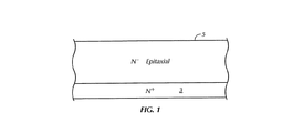
図1に関しては、強くドープされたN+基板3と軽くドープされたN−層5とを含む半導体ウエハの部分図が示されている。ここで用いられているように、導電率とは、記載の実施例に制限されるが、当業者であれば、P形導電率は、N形導電率に変えることができ、上記の半導体ディバイスはそれでも機能的には正しい(即ち、第1あるいは第2導電率形を用いると言っている。)ことが分かる。よって、ここで使用する場合、NまたはPと言っているのはNはPに置き換えることができ、PはNに置き換えることができることを意味する。 With reference to FIG. 1, a partial view of a semiconductor wafer comprising a heavily doped N + substrate 3 and a lightly doped N − layer 5 is shown. As used herein, conductivity is limited to the described embodiment, but those skilled in the art can change P-type conductivity to N-type conductivity, and the semiconductor device described above. Is still functionally correct (ie, it uses the first or second conductivity type). Thus, as used herein, saying N or P means that N can be replaced with P and P can be replaced with N.
図2に関しては、当業界で周知の技術を用いて、N−層5がエッチングされて、エッチングで形成された溝の底部が、N+基板3と、N−層5と間の界面に接触あるいは接近している。このエッチング方法で、溝9とメサ11とが形成されている。メサ11は、この方法で、トランジスタ装置をその上に形成する構造体を形成する、周囲の端子領域に対向する作動領域にあるので、“ディバイス・メサ”と言う。メサ11に隣接する溝9の幅(A)はその他の溝と比べてほぼ同じである。明確には図示していないが、溝9は、各々、溝埋め方法を容易にするため各底部より各頂部において1%から10%分広いほうが好ましい。よって、メサ11の側壁面は、エピタキシアル層5の第1主表面に対し所定の傾斜を維持する。溝9が、基板(強くドープされている領域)3に向け、エピタキシアル層5の第1主表面から第1深さ位置まで深さ(B)で伸びているが、基板(強くドープされた領域)3に到る全ての距離に亘って延びる必要はない。
With reference to FIG. 2, using techniques well known in the art, the N − layer 5 is etched and the bottom of the trench formed by etching contacts the interface between the N + substrate 3 and the N −
図3は、化学蒸着法(CVD)により、深さ約1〜3マイクロメータ(μm)の酸化物層7で各メサ11の頂部と各溝9とを被覆した後の複数個のメサ11と、複数個の溝9とを示す。
FIG. 3 shows a plurality of
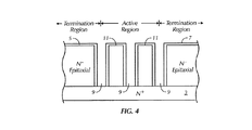
図4は、当業界では周知のタイプの乾式酸化物エッチング工程により、複数個の溝9の各々の底部から酸化物7を除去した後の図3の構造体を示す。
FIG. 4 shows the structure of FIG. 3 after
図5は、当業者には周知の方法でフォトレジストの層13を沈着させた後の図4の構造体を示す。
FIG. 5 shows the structure of FIG. 4 after deposition of a
図6は、マスク15(即ち、保護シールド)を置き、既知の反応体17を、マスク15では保護されない非保護フォトレジスト13に当てがった図5の構造体を示す。マスク15は、全ての端子領域と、作動領域と端子領域との間の境界に近接した所定の領域にある作動領域の一部との上に置くのが好ましい。既知の反応体17は紫外線光、深紫外線光、電子ビーム、X線等を含む。
FIG. 6 shows the structure of FIG. 5 with a mask 15 (ie, a protective shield) placed and a known
図7は、反応したフォトレジスト13は取り除かれ、反応しないフォトレジスト(以前はマスクの下にあったもの)が当業界では既知の場所に残っている図6の構造体を示す。
FIG. 7 shows the structure of FIG. 6 with the reacted
図8は、湿式酸化物エッチング工程でフォトレジスト13と、作動領域の各側の最後の溝の外壁上と、端子領域の頂部上の酸化物19以外の酸化物を除いた後の図7の構造体を示す。
FIG. 8 is a view of FIG. 7 after removing the
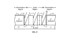
図9は、第1所定角度Φ(即ち、第1所定打込み角度Φ)で、図8の構造体へのイオン打込みを示す。第1所定打込み角度Φは、溝9の幅(A)と深さ(B)とで決定され、(即ち、A/B=打込み角度Φのタンジェント(正切))垂線から約2度から12度までである。イオンは、各溝9の底部に打込まれない角度Φで打ち込まれる。周囲の領域に打込みの拡散が起こらないよう溝9の底部へのイオンの打込みは回避される。イオンの打込みは、約30〜200キロ電子ボルト(keV)のエネルギー・レベルで、約1E13から1E14cm−2の範囲(即ち、約1x1013から1x1014 cm−2)のドープ量で行われる。よって、第1導電率形のドーパントは、複数個のメサと複数個の溝との所定領域の少なくとも1つのメサに、隣接する対の溝9において、1つの溝9の一側面で打込まれ、1つの溝9の一側面に、強くドープされた領域より低いドープ濃度を有する第1導電形の第1ドープ領域を形成する。図示のように、最後の溝9の外壁上の酸化物19(図9左側)がその面へのイオン打込みを阻止している。
FIG. 9 shows ion implantation into the structure of FIG. 8 at a first predetermined angle Φ (ie, a first predetermined implantation angle Φ). The first predetermined driving angle Φ is determined by the width (A) and depth (B) of the groove 9 (that is, A / B = tangent of the driving angle Φ (normal cutting)), approximately 2 degrees to 12 degrees from the perpendicular. Up to. Ions are implanted at an angle Φ that is not implanted into the bottom of each
図10は、第2所定角度Φ’(即ち、第2所定打込み角度Φ’)での、図9の構造体へのイオン打込みを示す。第2所定打込み角度Φ’も、溝9の幅(A)と深さ(B)とで決定され、(即ち、−A/B=打込み角度Φ’のタンジェント)垂線から約−2度から−12度までである。イオンは、各溝9の底部に打込まれない角度Φ’で打ち込まれる。第1所定打込み角度Φと第2所定打込み角度Φ’とはほぼ同じ大きさでも、少し異なっていても良い。周囲の領域に打込みの拡散が起こらないよう溝9の底部へのイオンの打込みは回避される。イオンの打込みは、約30−200keVのエネルギー・レベルで、約1E13から1E14cm−2の範囲のドープ量で行われる。よって、第2導電率形のドーパントは、複数個のメサ11と複数個の溝との所定領域の少なくとも1つのメサ11に、第1導電率形のドーパントが打込まれた側壁と対向している上記の少なくとも1つのメサの側壁面に打込まれ、第1導電率形のドーパントが打込まれた側壁に対向する側壁面に第2導電率形の第2ドープ領域を設け、複数個の溝9の少なくとも1つの深さ方向にそって位置する第1および第2ドープ領域のP−N接合を形成すると共に、作動領域の、イオンが打込まれていない外側壁を設ける。図示のように、最後の溝9の外壁上の酸化物19(図9右側)がその面へのイオン打込みを阻止している。
FIG. 10 shows ion implantation into the structure of FIG. 9 at a second predetermined angle Φ ′ (ie, a second predetermined implantation angle Φ ′). The second predetermined driving angle Φ ′ is also determined by the width (A) and depth (B) of the groove 9 (that is, −A / B = tangent of the driving angle Φ ′) from about −2 degrees from the perpendicular line − It is up to 12 degrees. Ions are implanted at an angle Φ ′ that is not implanted into the bottom of each
図11は、図9と図10の構造体の溝9から酸化物19が除去された後の第10の構造体に形成されている超接合装置を示す。全ての溝9に絶縁材料28が充填され、頂面が平坦化されている。構造体に超接合装置を製造した後イオン打込み22を行い、イオンを打込んだ領域にゲート20を沈着し、ゲート導電体26およびゲート酸化物24を加える。これら全ては、当業界で既知の方法で為される。よって、ゲート電極層20は、溝9の少なくとも1つでその第1主表面上に形成される。ゲート電極層20は、第1ドープ領域とオーム接触しているが、ショットキー(Schottky)接触しているほうが好ましい。
FIG. 11 shows the superjunction device formed in the tenth structure after the
この構造体に建造ないし形成された装置の性能は、従来の半導体トランジスタ装置に比べて、雪崩破壊電圧(Vb)特性が向上している。第2ドープ領域と電気的に連結する第3ドープ領域を第1および第2ドープ領域の第1主表面に設け、第1導電率形の第4ドープ領域を、これが第3ドープ領域を挟んで第1ドープ領域と対向するように、上記の1つの溝9の第1主表面と側壁面の1方あるいは両方に設けることにより追加の打込みをすることもできる。ゲート電極層20は、第1ドープ領域と第4ドープ領域との間で、ゲート絶縁層を介在させて第3ドープ領域に対向させて設けられている。
As for the performance of the device constructed or formed in this structure, the avalanche breakdown voltage (Vb) characteristics are improved as compared with the conventional semiconductor transistor device. A third doped region electrically connected to the second doped region is provided on the first main surface of the first and second doped regions, and a fourth doped region of the first conductivity type is sandwiched by the third doped region. Additional implantation can be performed by providing the first
図12から図17図は、本発明の第2実施例による、従来の端子を備えた超接合装置を製造する方法を示す。 12 to 17 show a method of manufacturing a superjunction device having a conventional terminal according to a second embodiment of the present invention.
図12は、酸化物の沈着とその後の溝9の側壁と底部とのエッチング後の図2の構造体を示す。
FIG. 12 shows the structure of FIG. 2 after oxide deposition and subsequent etching of the sidewalls and bottom of the
図13は、マスク(図示されていないが、図6のマスクと同様のもの)が、作動領域の片側の最後の溝9(左側)と、これに隣接するメサ領域の一部にのみフォトレジスト23を沈着するため置かれ、フォトレジスト23が沈着された後の図12の構造体を示す。フォトレジスト23が溝の両側壁へのイオンの打込みを阻止する。
FIG. 13 shows a mask (not shown but similar to the mask of FIG. 6) in which the photoresist is applied only to the last groove 9 (left side) on one side of the working area and a part of the mesa area adjacent to it. FIG. 13 shows the structure of FIG. 12 after being deposited for depositing 23 and the
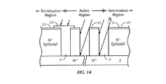
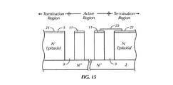
図15は、第1所定角度Φでの、図13の構造体へのイオン打込みを示す。第1所定角度Φは、溝9の幅(A)と深さ(B)とで決定され、(即ち、A/B=打込み角度Φのタンジェント)垂線から約2度から12度までである。イオンは、各溝9の底部に打込まれない角度Φで打ち込まれる。周囲の領域に打込みの拡散が起こらないよう溝9の底部へのイオンの打込みは回避される。イオンの打込みは、約30〜200keVのエネルギー・レベルで、約1E13から1E14cm−2の範囲のドープ量で行われる。よって、第1導電率形のドーパントは、複数個のメサ11と複数個の溝9との所定領域のとくなくとも1つのメサに、隣接対の溝9において、1つの溝9の側壁面で、打込まれ、上記の1つの溝9の一側面に、強くドープされた領域より低いドープ濃度を有する第1導電形の第1ドープ領域を形成する。図示のように、最後の溝9のフォトレジスト23(左側)が溝9へのイオン打込みを阻止している。
FIG. 15 shows ion implantation into the structure of FIG. 13 at a first predetermined angle Φ. The first predetermined angle Φ is determined by the width (A) and depth (B) of the groove 9 (ie, A / B = tangent of the driving angle Φ) and is about 2 to 12 degrees from the perpendicular. Ions are implanted at an angle Φ that is not implanted into the bottom of each
図15は、マスク(図示されていないが、図6のマスクと同様のもの)を、最後の溝9(右側)と、図13のフォトレジスト23の位置とは反対側の作動領域側の、この溝と隣接するメサ領域の一部にのみフォトレジスト25を沈着するため置かれ、フォトレジスト25が沈着された後の図14の構造体を示す。フォトレジスト25は溝の両側壁へのイオンの打込みを阻止する。
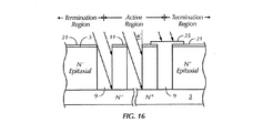
15 shows a mask (not shown but similar to the mask of FIG. 6) on the side of the working region opposite to the position of the last groove 9 (right side) and the
図16は、第2所定角度Φ’(即ち、第2所定打込み角度Φ’)での、図15の構造体へのイオン打込みを示す。第2所定打込み角度Φ’は、溝の幅(A)と深さ(B)とで決定され、(即ち、−(A/B)=打込み角度Φ’のタンジェントで)垂線から約−2度から−12度までである。イオンは、各溝9の底部に打込まれない角度Φ’で打ち込まれる。周囲の領域に打込みの拡散が起こらないよう溝9の底部にはイオンの打込みは回避される。イオンの打込みは、約30から200keVのエネルギー・レベルで、約1E13から1E14cm−2の範囲のドープ量で行われる。よって、第2導電率形のドーパントは、複数個のメサ11と複数個の溝との所定領域の少なくとも1つのメサ11に、第1導電率形のドーパントが打込まれた側壁に対向する上記の少なくとも1つのメサの側壁面で、打込まれ、第1導電率形のドーパントが打込まれた側壁に対向する側壁面に第2導電率形の第2ドープ領域を設け、複数個の溝9の少なくとも1つの深さ方向にそって位置する第1および第2ドープ領域のP−N接合を形成すると共に、作動領域の、イオンが打込まれていない外側壁を設ける。図示のように、最後の溝9のフォトレジスト25(右側)が溝9へのイオン打込みを阻止している。
FIG. 16 shows ion implantation into the structure of FIG. 15 at a second predetermined angle Φ ′ (ie, a second predetermined implantation angle Φ ′). The second predetermined driving angle Φ ′ is determined by the width (A) and depth (B) of the groove and is about −2 degrees from the perpendicular (ie, − (A / B) = tangent of driving angle Φ ′). To -12 degrees. Ions are implanted at an angle Φ ′ that is not implanted into the bottom of each
よって、第2の好ましい実施例では、最後の溝9(図中右あるいは左)上にフォトレジスト23、25が置かれ、溝9へのイオンの打込みが阻止されている。構造体の他端での最後の溝9へのイオンの打込みも同様に阻止される。最後の溝9(図中右と左)へのイオンの打込みを阻止することにより、基板上に形成されるディバイスの雪崩破壊電圧(Vb)の劣化を防ぐ。フォトレジスト23,25はイオン打込み後メサ11及び溝9から取り除けられる。
Thus, in the second preferred embodiment,
図17は、図14に示されているフォトレジスト23と図16に示されているフォトレジスト25が構造体から除去され、溝9に絶縁材料28が充填され、頂面が平坦化された後の図16に対応する構造体を示す。構造体に超接合装置を製造した後イオン打込み22を行い、イオンを打込んだ領域にゲート20を沈着し、ゲート導電体26およびゲート酸化物24を加える。これら全ては、当業界で既知の方法で為される。よって、ゲート電極層20は、溝9の少なくとも1つでその主表面上に形成される。ゲート電極層20は、第1ドープ領域とオーム接触しているが、ショットキー(Schottky)接触しているほうが好ましい。この構造体に建造ないし形成された装置の性能は、従来の半導体トランジスタ装置に比べて、雪崩破壊電圧(Vb)特徴が向上している。
17 shows that after the
第2ドープ領域のP−N接合を提供する。そして作動領域上に従来のMOS電界効果トランジスタ(MOSFET)装置が、ゲート酸化物層24の形成、ゲート導電体26の沈着と形成およびゲート電極20の沈着を含む周知の工程を用いて、作製される。選択的に第2導電率形の作動領域を打込み、その後選択的に第1導電率形の領域を打込む追加の工程によりディバイスが完成する。前面の領域と後面への接点も作られ、不動態化層が沈着され、パターン化されディバイスの製造順序が終了する。
A PN junction in the second doped region is provided. A conventional MOS field effect transistor (MOSFET) device is then fabricated on the active region using well known processes including the formation of the
上記より、本発明は、半導体ディバイスおよび半導体ディバイスの製造方法に関する。当業者であれば、上記の実施例には、その広い発明概念から逸脱することなく変形が可能であることが感得せられる。よって、本発明は、開示されている特定の実施例に限定されるものではなく、本発明の精神内の変形例もカバーするものである。 As described above, the present invention relates to a semiconductor device and a method for manufacturing the semiconductor device. Those skilled in the art will appreciate that the above embodiments can be modified without departing from the broad inventive concept. Thus, the present invention is not limited to the specific embodiments disclosed, but covers variations within the spirit of the invention.
Claims (14)
相互に対向する第1及び第2の主表面を有する半導体基板を設け、上記の半導体基板は、第2主表面に第1導電率形の強くドープされた領域を有し、第1主表面に第1導電率形の軽くドープされた領域を有し、
上記の半導体基板において、その作動領域に複数個の溝と複数個のメサとをエッチングにより設け、各溝は、強くドープされた領域に向け、第1主表面から第1深さ位置まで伸びる第1延長部分を有し、各メサは、第1主表面に対し所定の傾斜を維持する側壁面を有し、上記の複数個の溝の各々は、複数個のメサの1つにより、その他の溝の各々から離れていて、
作動領域と、作動領域の外側およびこれに隣接する端子領域内に延びる、複数個のメサと複数個の溝との所定領域を、各メサの頂部、複数個の溝の各々の両側面および底部ならびに端子領域の頂部を酸化物が覆うまで酸化し、
複数個のメサと複数個の溝との所定領域を、乾式酸化物エンチング法を用いてエッチングし、複数個の溝の底部にある酸化物を除去し、
作動領域と端子領域との間の境界の所定領域上に保護シールドを形成し、
その後複数個のメサと複数個の溝との所定領域の上から保護シールドを部分的に除去し、
複数個のメサと複数個の溝との所定領域の少なくとも1つの所定のメサに、隣接対の溝において、1つの溝の側壁面で、第1導電率形のドーパントを、第1所定打込み角度で打込み、上記の1つの溝の側壁面に、強くドープされた領域より低いドープ濃度を有する第1導電率形の第1ドープ領域を形成し、
複数個のメサと複数個の溝との所定領域の少なくとも1つのメサに、第1導電率形のドーパントを打込んだ側壁に対向する上記の少なくとも1つのメサの側壁面で、第2導電率形のドーパントを、第2所定打込み角度で打込んで、第1導電率形のドーパントを打込んだ側壁に対向する側壁面に第2導電率形の第2ドープ領域を設けて、複数個の溝の少なくとも1つの溝の深さ方向に沿って位置する第1および第2ドープ領域のP−N接合を形成すると共に、作動領域のイオンが打込まれていない外側壁を設け、
複数個の溝に絶縁材料を充填し、
構造体の頂面を平坦化して、
超接合装置をこの構造体上に形成するもの。 A method for manufacturing a semiconductor device, comprising:
A semiconductor substrate having first and second main surfaces opposite to each other is provided, and the semiconductor substrate has a strongly doped region of the first conductivity type on the second main surface, and the first main surface has Having a lightly doped region of the first conductivity type;
In the semiconductor substrate, a plurality of grooves and a plurality of mesas are provided by etching in the operation region, and each groove extends from the first main surface to the first depth position toward the strongly doped region. Each mesa has a side wall surface that maintains a predetermined inclination with respect to the first main surface, and each of the plurality of grooves is formed by one of the plurality of mesas. Away from each of the grooves,
A predetermined region of a plurality of mesas and a plurality of grooves extending in the operation region and outside the operation region and in a terminal region adjacent thereto, the top of each mesa, each side surface and the bottom of each of the plurality of grooves And oxidize the top of the terminal area until the oxide covers it,
A predetermined region of the plurality of mesas and the plurality of grooves is etched using a dry oxide enching method to remove the oxide at the bottom of the plurality of grooves,
Forming a protective shield on a predetermined area at the boundary between the operating area and the terminal area;
Thereafter, the protective shield is partially removed from above the predetermined area of the plurality of mesas and the plurality of grooves,
At least one predetermined mesa in a predetermined region of a plurality of mesas and a plurality of grooves, a first conductivity type dopant is applied to a first pair of grooves on a side wall surface of one groove in an adjacent pair of grooves. To form a first doped region of the first conductivity type having a lower doping concentration than the strongly doped region on the sidewall surface of the one groove,
At least one mesa in a predetermined region of the plurality of mesas and the plurality of grooves has a second conductivity on the side wall surface of the at least one mesa facing the side wall in which the dopant of the first conductivity type is implanted. A second doped region of the second conductivity type is provided on the side wall surface opposite to the side wall into which the dopant of the first conductivity type is implanted, and a plurality of dopants of the second conductivity type are implanted at a second predetermined implantation angle; Forming a PN junction of the first and second doped regions located along the depth direction of at least one of the grooves, and providing an outer wall not implanted with ions in the working region;
Fill multiple grooves with insulating material,
Flatten the top surface of the structure,
A super junction device is formed on this structure.
複数個のメサと複数個の溝との所定領域の上にフォトレジストの層を沈着させ、
複数個のメサと複数個の溝との所定領域の各側の最後の溝の外側壁上のフォトレジストが保護され、上記の所定領域の残りの個所は保護されないように、マスクを置き、
フォトレジストの保護されていない部分を、紫外線光、深紫外線光、電子ビームおよびX線を含むグループから選ばれたフォトレジスト反応体に晒すことからなるものにおいて、
上記の保護シールドを部分的に除去する工程が、
複数個のメサと複数個の溝との所定領域上からマスクを除き、
反応したフォトレジストを構造体から取除き、
複数個のメサと複数個の溝の所定領域を湿式酸化物エッチング法によりエッチングして、反応しなかったフォトレジストにより酸化物が保護されていた上記の所定領域の各側の最後の溝の外側壁をのぞいて、上記の所定領域から反応しなかったフォトレジストと酸化物とを除去し、上記の酸化物は上記の各最後の溝の外側壁へのイオン打込みを阻止するため残されているもの。 The method of manufacturing a semiconductor device according to claim 1, wherein the step of forming a protective shield comprises:
Depositing a layer of photoresist over a predetermined area of the plurality of mesas and the plurality of grooves;
Place the mask so that the photoresist on the outer wall of the last groove on each side of the predetermined area of the plurality of mesas and the plurality of grooves is protected, and the remaining portions of the predetermined area are not protected,
In exposing the unprotected portion of the photoresist to a photoresist reactant selected from the group comprising ultraviolet light, deep ultraviolet light, electron beam and X-rays,
The step of partially removing the protective shield
The mask is removed from a predetermined area of the plurality of mesas and the plurality of grooves,
Remove the reacted photoresist from the structure,
The predetermined region of the plurality of mesas and the plurality of grooves is etched by a wet oxide etching method, and the oxide is protected by the unreacted photoresist. The outside of the last groove on each side of the predetermined region Except for the walls, the unreacted photoresist and oxide are removed from the predetermined region, and the oxide remains to prevent ion implantation into the outer wall of each last groove. thing.
第2ドープ領域と電気的に連結する第3ドープ領域を第1および第2ドープ領域の第1主表面に設け、
第1導電率形の第4ドープ領域を、これが第3ドープ領域を挟んで第1ドープ領域と対向するように、上記の1つの溝の第1主表面と側壁面の少なくとも一方に設け、
ゲート電極層を、第1ドープ領域と第4ドープ領域との間で、ゲート絶縁層を介在させて第3ドープ領域に対向させて設けることからなるもの。 A method of manufacturing a semiconductor device according to claim 2,
Providing a third doped region electrically connected to the second doped region on the first main surface of the first and second doped regions;
A fourth conductivity region of the first conductivity type is provided on at least one of the first main surface and the side wall surface of the one groove so that the fourth conductivity region faces the first doping region across the third doping region;
A gate electrode layer is provided between the first doped region and the fourth doped region so as to face the third doped region with a gate insulating layer interposed therebetween.
複数個のメサと複数個の溝との所定領域を乾式酸化物エッチング法を用いてエッチングして、複数個の溝の各々の両側部と底部とにある酸化物を除去し、
マスクを、このマスクの開口部のみが、作動領域の各側の最後の溝とこれに隣接するメサ領域上に位置するように位置決めし、
作動領域の最後の溝とこれに隣接するメサ領域のみが、フォトレジストが沈着する領域であるようにフォトレジストの層をマスク上に沈着させることからなるものにおいて、
部分的に保護シールドを除去する工程が、最後の溝とこれに隣接するメサ領域とを除いて、フォトレジストが沈着するのを阻止したマスクを除去することからなるもの。 The method of manufacturing a semiconductor device according to claim 1, wherein the step of forming a protective shield comprises:
Etching a predetermined region of the plurality of mesas and the plurality of grooves using a dry oxide etching method to remove oxides on both sides and the bottom of each of the plurality of grooves;
Positioning the mask so that only the opening of the mask is located on the last groove on each side of the working area and the mesa area adjacent to it;
In what consists of depositing a layer of photoresist on the mask so that only the last groove of the active area and the mesa area adjacent to it are areas where the photoresist is deposited,
The step of partially removing the protective shield comprises removing the mask that prevented the deposition of the photoresist, except for the last trench and the mesa region adjacent thereto.
第2ドープ領域と電気的に連結する第3ドープ領域を第1および第2ドープ領域の第1主表面に設け、
第1導電率形の第4ドープ領域を、これが第3ドープ領域を挟んで第1ドープ領域と対向するように、上記の複数個の溝の第1主表面と側壁面のいずれか一方に設け、
ゲート電極層を、第1ドープ領域と第4ドープ領域との間で、ゲート絶縁層を介在させて第3ドープ領域に対向させて設けることからなるもの。 A method of manufacturing a semiconductor device according to claim 6, further comprising:
Providing a third doped region electrically connected to the second doped region on the first main surface of the first and second doped regions;
A fourth doped region of the first conductivity type is provided on one of the first main surface and the side wall surface of the plurality of grooves so as to face the first doped region across the third doped region. ,
A gate electrode layer is provided between the first doped region and the fourth doped region so as to face the third doped region with a gate insulating layer interposed therebetween.
第2ドープ領域と電気的に連結する第3ドープ領域を第1および第2ドープ領域の第1主表面に設けることからなるもの。 A method of manufacturing a semiconductor device according to claim 6, further comprising:
A third doped region electrically connected to the second doped region is provided on the first main surface of the first and second doped regions.
半導体ディバイスの製造において第1および第2導電率形のドーパントの各々の拡散長さが、隣接対の側壁面から、第1および第2ドープ領域のP−N接合までの距離より長いもの。 A method of manufacturing a semiconductor device according to claim 6, further comprising:
In the manufacture of semiconductor devices, the diffusion length of each of the first and second conductivity type dopants is longer than the distance from the adjacent pair of sidewall surfaces to the PN junctions of the first and second doped regions.
第2ドープ領域と電気的に連結する第3ドープ領域を第1および第2ドープ領域の第1主表面に設けることからなるもの。 A method of manufacturing a semiconductor device according to claim 1, further comprising:
A third doped region electrically connected to the second doped region is provided on the first main surface of the first and second doped regions.
電極層を第1ドープ領域とショットキー(Schottky)接触させることからなるもの。 A method of manufacturing a semiconductor device according to claim 1, further comprising:
It consists of bringing the electrode layer into Schottky contact with the first doped region.
半導体ディバイスの製造において第1および第2導電率形のドーパントの各々の拡散長さが、隣接対の溝の側壁面から、第1および第2ドープ領域のP−N接合までの距離より長いもの。
A method of manufacturing a semiconductor device according to claim 1,
In the manufacture of semiconductor devices, the diffusion length of each of the first and second conductivity type dopants is longer than the distance from the sidewall surface of the adjacent pair of grooves to the PN junction of the first and second doped regions .
Applications Claiming Priority (2)
| Application Number | Priority Date | Filing Date | Title |
|---|---|---|---|
| US53150103P | 2003-12-19 | 2003-12-19 | |
| PCT/US2004/041302 WO2005065140A2 (en) | 2003-12-19 | 2004-12-10 | Method of manufacturing a superjunction device with conventional terminations |
Related Child Applications (1)
| Application Number | Title | Priority Date | Filing Date |
|---|---|---|---|
| JP2008227992A Division JP5154347B2 (en) | 2003-12-19 | 2008-09-05 | Superjunction semiconductor device and method of manufacturing superjunction semiconductor device |
Publications (2)
| Publication Number | Publication Date |
|---|---|
| JP2007515079A true JP2007515079A (en) | 2007-06-07 |
| JP2007515079A5 JP2007515079A5 (en) | 2008-10-23 |
Family
ID=34748768
Family Applications (2)
| Application Number | Title | Priority Date | Filing Date |
|---|---|---|---|
| JP2006545755A Pending JP2007515079A (en) | 2003-12-19 | 2004-12-10 | Manufacturing method of super-junction device with conventional terminal |
| JP2008227992A Expired - Fee Related JP5154347B2 (en) | 2003-12-19 | 2008-09-05 | Superjunction semiconductor device and method of manufacturing superjunction semiconductor device |
Family Applications After (1)
| Application Number | Title | Priority Date | Filing Date |
|---|---|---|---|
| JP2008227992A Expired - Fee Related JP5154347B2 (en) | 2003-12-19 | 2008-09-05 | Superjunction semiconductor device and method of manufacturing superjunction semiconductor device |
Country Status (6)
| Country | Link |
|---|---|
| US (2) | US7041560B2 (en) |
| EP (1) | EP1701686A4 (en) |
| JP (2) | JP2007515079A (en) |
| KR (2) | KR20080100265A (en) |
| TW (1) | TWI368948B (en) |
| WO (1) | WO2005065140A2 (en) |
Cited By (1)
| Publication number | Priority date | Publication date | Assignee | Title |
|---|---|---|---|---|
| JP2007515080A (en) * | 2003-12-19 | 2007-06-07 | サード ディメンジョン (スリーディ) セミコンダクタ インコーポレイテッド | Planarization method in the manufacture of superjunction devices |
Families Citing this family (43)
| Publication number | Priority date | Publication date | Assignee | Title |
|---|---|---|---|---|
| US7638841B2 (en) | 2003-05-20 | 2009-12-29 | Fairchild Semiconductor Corporation | Power semiconductor devices and methods of manufacture |
| KR100994719B1 (en) | 2003-11-28 | 2010-11-16 | 페어차일드코리아반도체 주식회사 | Superjunction semiconductor device |
| KR20080100265A (en) * | 2003-12-19 | 2008-11-14 | 써드 디멘존 세미컨덕터, 인코포레이티드 | Method of manufacturing a superjunction device with conventional terminations |
| US6982193B2 (en) * | 2004-05-10 | 2006-01-03 | Semiconductor Components Industries, L.L.C. | Method of forming a super-junction semiconductor device |
| US7439583B2 (en) * | 2004-12-27 | 2008-10-21 | Third Dimension (3D) Semiconductor, Inc. | Tungsten plug drain extension |
| TWI401749B (en) * | 2004-12-27 | 2013-07-11 | Third Dimension 3D Sc Inc | Process for high voltage superjunction termination |
| US20090026586A1 (en) * | 2005-04-22 | 2009-01-29 | Icemos Technology Corporation | Superjunction Device Having Oxide Lined Trenches and Method for Manufacturing a Superjunction Device Having Oxide Lined Trenches |
| US7446018B2 (en) | 2005-08-22 | 2008-11-04 | Icemos Technology Corporation | Bonded-wafer superjunction semiconductor device |
| US7429772B2 (en) * | 2006-04-27 | 2008-09-30 | Icemos Technology Corporation | Technique for stable processing of thin/fragile substrates |
| US7948033B2 (en) | 2007-02-06 | 2011-05-24 | Semiconductor Components Industries, Llc | Semiconductor device having trench edge termination structure |
| US8580651B2 (en) * | 2007-04-23 | 2013-11-12 | Icemos Technology Ltd. | Methods for manufacturing a trench type semiconductor device having a thermally sensitive refill material |
| US7723172B2 (en) | 2007-04-23 | 2010-05-25 | Icemos Technology Ltd. | Methods for manufacturing a trench type semiconductor device having a thermally sensitive refill material |
| CN101868856B (en) | 2007-09-21 | 2014-03-12 | 飞兆半导体公司 | Superjunction structures for power devices and methods of manufacture |
| US8012806B2 (en) | 2007-09-28 | 2011-09-06 | Icemos Technology Ltd. | Multi-directional trenching of a die in manufacturing superjunction devices |
| US9484451B2 (en) | 2007-10-05 | 2016-11-01 | Vishay-Siliconix | MOSFET active area and edge termination area charge balance |
| ITMI20072341A1 (en) * | 2007-12-14 | 2009-06-15 | St Microelectronics Srl | DEPTH CONTACTS OF INTEGRATED ELECTRONIC DEVICES BASED ON REGIONS PLANTED THROUGH SHEARS |
| CN101510557B (en) * | 2008-01-11 | 2013-08-14 | 艾斯莫斯技术有限公司 | Superjunction device having a dielectric termination and methods for manufacturing the device |
| US7846821B2 (en) | 2008-02-13 | 2010-12-07 | Icemos Technology Ltd. | Multi-angle rotation for ion implantation of trenches in superjunction devices |
| US7795045B2 (en) * | 2008-02-13 | 2010-09-14 | Icemos Technology Ltd. | Trench depth monitor for semiconductor manufacturing |
| US8030133B2 (en) | 2008-03-28 | 2011-10-04 | Icemos Technology Ltd. | Method of fabricating a bonded wafer substrate for use in MEMS structures |
| US7807576B2 (en) * | 2008-06-20 | 2010-10-05 | Fairchild Semiconductor Corporation | Structure and method for forming a thick bottom dielectric (TBD) for trench-gate devices |
| US20120273916A1 (en) | 2011-04-27 | 2012-11-01 | Yedinak Joseph A | Superjunction Structures for Power Devices and Methods of Manufacture |
| US20110198689A1 (en) * | 2010-02-17 | 2011-08-18 | Suku Kim | Semiconductor devices containing trench mosfets with superjunctions |
| US8598654B2 (en) | 2011-03-16 | 2013-12-03 | Fairchild Semiconductor Corporation | MOSFET device with thick trench bottom oxide |
| US8772868B2 (en) | 2011-04-27 | 2014-07-08 | Fairchild Semiconductor Corporation | Superjunction structures for power devices and methods of manufacture |
| US8786010B2 (en) | 2011-04-27 | 2014-07-22 | Fairchild Semiconductor Corporation | Superjunction structures for power devices and methods of manufacture |
| US8836028B2 (en) | 2011-04-27 | 2014-09-16 | Fairchild Semiconductor Corporation | Superjunction structures for power devices and methods of manufacture |
| US8673700B2 (en) | 2011-04-27 | 2014-03-18 | Fairchild Semiconductor Corporation | Superjunction structures for power devices and methods of manufacture |
| CN103094067B (en) * | 2011-10-31 | 2015-10-14 | 上海华虹宏力半导体制造有限公司 | A kind of manufacture method of semiconductor device |
| US9431249B2 (en) | 2011-12-01 | 2016-08-30 | Vishay-Siliconix | Edge termination for super junction MOSFET devices |
| US9614043B2 (en) | 2012-02-09 | 2017-04-04 | Vishay-Siliconix | MOSFET termination trench |
| TWI446459B (en) * | 2012-02-14 | 2014-07-21 | Anpec Electronics Corp | Manufacturing method of power transistor device with super junction |
| US8946814B2 (en) | 2012-04-05 | 2015-02-03 | Icemos Technology Ltd. | Superjunction devices having narrow surface layout of terminal structures, buried contact regions and trench gates |
| US9842911B2 (en) | 2012-05-30 | 2017-12-12 | Vishay-Siliconix | Adaptive charge balanced edge termination |
| US9576842B2 (en) | 2012-12-10 | 2017-02-21 | Icemos Technology, Ltd. | Grass removal in patterned cavity etching |
| US9508596B2 (en) | 2014-06-20 | 2016-11-29 | Vishay-Siliconix | Processes used in fabricating a metal-insulator-semiconductor field effect transistor |
| US9887259B2 (en) | 2014-06-23 | 2018-02-06 | Vishay-Siliconix | Modulated super junction power MOSFET devices |
| KR102098996B1 (en) | 2014-08-19 | 2020-04-08 | 비쉐이-실리코닉스 | Super-junction metal oxide semiconductor field effect transistor |
| CN104465402B (en) * | 2014-12-25 | 2018-03-06 | 中航(重庆)微电子有限公司 | A kind of semiconductor device fabrication processes |
| DE102018130444A1 (en) | 2018-11-30 | 2020-06-04 | Infineon Technologies Austria Ag | Method of making a superjunction transistor device |
| CN111628034B (en) * | 2020-05-28 | 2023-09-15 | 湖北京邦科技有限公司 | Method for manufacturing photoelectric detection device |
| CN112289684B (en) * | 2020-10-28 | 2023-06-30 | 上海华虹宏力半导体制造有限公司 | Manufacturing method of power device and device |
| US11769665B2 (en) * | 2022-01-11 | 2023-09-26 | Applied Materials, Inc. | Power device structures and methods of making |
Family Cites Families (59)
| Publication number | Priority date | Publication date | Assignee | Title |
|---|---|---|---|---|
| US4158206A (en) * | 1977-02-07 | 1979-06-12 | Rca Corporation | Semiconductor device |
| JPS5553462A (en) * | 1978-10-13 | 1980-04-18 | Int Rectifier Corp | Mosfet element |
| US5057444A (en) * | 1985-03-05 | 1991-10-15 | Matsushita Electric Industrial Co., Ltd. | Method of fabricating semiconductor device |
| US5019522A (en) * | 1986-03-21 | 1991-05-28 | Advanced Power Technology, Inc. | Method of making topographic pattern delineated power MOSFET with profile tailored recessed source |
| US4895810A (en) * | 1986-03-21 | 1990-01-23 | Advanced Power Technology, Inc. | Iopographic pattern delineated power mosfet with profile tailored recessed source |
| US5045903A (en) * | 1988-05-17 | 1991-09-03 | Advanced Power Technology, Inc. | Topographic pattern delineated power MOSFET with profile tailored recessed source |
| US5472888A (en) * | 1988-02-25 | 1995-12-05 | International Rectifier Corporation | Depletion mode power MOSFET with refractory gate and method of making same |
| CN1019720B (en) * | 1991-03-19 | 1992-12-30 | 电子科技大学 | Power semiconductor device |
| DE69220846T2 (en) * | 1991-05-03 | 1998-02-12 | Philips Electronics Nv | Method for manufacturing a semiconductor device with ion implantation |
| JPH05304297A (en) * | 1992-01-29 | 1993-11-16 | Nec Corp | Semiconductor power device and manufacture thereof |
| JPH0653315A (en) * | 1992-07-30 | 1994-02-25 | Nec Corp | Semiconductor device and manufacture thereof |
| US5506421A (en) * | 1992-11-24 | 1996-04-09 | Cree Research, Inc. | Power MOSFET in silicon carbide |
| CN1035294C (en) * | 1993-10-29 | 1997-06-25 | 电子科技大学 | Withstand voltage layer with special shaped doped island for semiconductor device |
| US5435888A (en) * | 1993-12-06 | 1995-07-25 | Sgs-Thomson Microelectronics, Inc. | Enhanced planarization technique for an integrated circuit |
| DE4404757C2 (en) * | 1994-02-15 | 1998-08-20 | Siemens Ag | Method for producing a diffusion region adjacent to a trench in a substrate |
| JP4047384B2 (en) * | 1996-02-05 | 2008-02-13 | シーメンス アクチエンゲゼルシヤフト | Semiconductor devices that can be controlled by field effects |
| US5744994A (en) * | 1996-05-15 | 1998-04-28 | Siliconix Incorporated | Three-terminal power mosfet switch for use as synchronous rectifier or voltage clamp |
| KR0183886B1 (en) * | 1996-06-17 | 1999-04-15 | 김광호 | Trench element isolation method of semiconductor device |
| JP3327135B2 (en) * | 1996-09-09 | 2002-09-24 | 日産自動車株式会社 | Field effect transistor |
| JP3607016B2 (en) * | 1996-10-02 | 2005-01-05 | 株式会社半導体エネルギー研究所 | Semiconductor device and manufacturing method thereof, and portable information processing terminal, head mounted display, navigation system, mobile phone, camera, and projector |
| JP3938964B2 (en) * | 1997-02-10 | 2007-06-27 | 三菱電機株式会社 | High voltage semiconductor device and manufacturing method thereof |
| CN1199926A (en) * | 1997-05-21 | 1998-11-25 | 日本电气株式会社 | Method of fabricating semiconductor device capable of providing mosfet which is improved in threshold voltage thereof |
| JP3618517B2 (en) * | 1997-06-18 | 2005-02-09 | 三菱電機株式会社 | Semiconductor device and manufacturing method thereof |
| US5976947A (en) * | 1997-08-18 | 1999-11-02 | Micron Technology, Inc. | Method for forming dielectric within a recess |
| US6239463B1 (en) * | 1997-08-28 | 2001-05-29 | Siliconix Incorporated | Low resistance power MOSFET or other device containing silicon-germanium layer |
| US6081009A (en) * | 1997-11-10 | 2000-06-27 | Intersil Corporation | High voltage mosfet structure |
| DE19801095B4 (en) | 1998-01-14 | 2007-12-13 | Infineon Technologies Ag | Power MOSFET |
| DE69818289T2 (en) * | 1998-07-23 | 2004-07-01 | Mitsubishi Denki K.K. | Method for producing a semiconductor device and semiconductor device that can be produced thereby |
| US6265282B1 (en) * | 1998-08-17 | 2001-07-24 | Micron Technology, Inc. | Process for making an isolation structure |
| US6355580B1 (en) * | 1998-09-03 | 2002-03-12 | Micron Technology, Inc. | Ion-assisted oxidation methods and the resulting structures |
| JP3951522B2 (en) * | 1998-11-11 | 2007-08-01 | 富士電機デバイステクノロジー株式会社 | Super junction semiconductor device |
| US6291856B1 (en) * | 1998-11-12 | 2001-09-18 | Fuji Electric Co., Ltd. | Semiconductor device with alternating conductivity type layer and method of manufacturing the same |
| DE19854915C2 (en) * | 1998-11-27 | 2002-09-05 | Infineon Technologies Ag | MOS field effect transistor with auxiliary electrode |
| EP1011146B1 (en) * | 1998-12-09 | 2006-03-08 | STMicroelectronics S.r.l. | Method of manufacturing an integrated edge structure for high voltage semiconductor devices |
| US6452230B1 (en) * | 1998-12-23 | 2002-09-17 | International Rectifier Corporation | High voltage mosgated device with trenches to reduce on-resistance |
| US6190970B1 (en) * | 1999-01-04 | 2001-02-20 | Industrial Technology Research Institute | Method of making power MOSFET and IGBT with optimized on-resistance and breakdown voltage |
| US6346442B1 (en) * | 1999-02-04 | 2002-02-12 | Tower Semiconductor Ltd. | Methods for fabricating a semiconductor chip having CMOS devices and a fieldless array |
| US6222229B1 (en) * | 1999-02-18 | 2001-04-24 | Cree, Inc. | Self-aligned shield structure for realizing high frequency power MOSFET devices with improved reliability |
| US6198127B1 (en) * | 1999-05-19 | 2001-03-06 | Intersil Corporation | MOS-gated power device having extended trench and doping zone and process for forming same |
| EP1058303A1 (en) * | 1999-05-31 | 2000-12-06 | STMicroelectronics S.r.l. | Fabrication of VDMOS structure with reduced parasitic effects |
| DE19964214C2 (en) * | 1999-09-07 | 2002-01-17 | Infineon Technologies Ag | Method for producing a drift zone of a compensation component |
| GB9929613D0 (en) * | 1999-12-15 | 2000-02-09 | Koninkl Philips Electronics Nv | Manufacture of semiconductor material and devices using that material |
| US6214698B1 (en) * | 2000-01-11 | 2001-04-10 | Taiwan Semiconductor Manufacturing Company | Shallow trench isolation methods employing gap filling doped silicon oxide dielectric layer |
| JP4483001B2 (en) * | 2000-02-17 | 2010-06-16 | 富士電機システムズ株式会社 | Semiconductor element |
| JP4560181B2 (en) * | 2000-06-30 | 2010-10-13 | アイシン高丘株式会社 | Method and apparatus for manufacturing fuel cell separator |
| JP2002170955A (en) * | 2000-09-25 | 2002-06-14 | Toshiba Corp | Semiconductor device and its manufacturing method |
| JP4088031B2 (en) * | 2000-10-16 | 2008-05-21 | 株式会社東芝 | Semiconductor device and manufacturing method thereof |
| US6509220B2 (en) * | 2000-11-27 | 2003-01-21 | Power Integrations, Inc. | Method of fabricating a high-voltage transistor |
| JP4088033B2 (en) * | 2000-11-27 | 2008-05-21 | 株式会社東芝 | Semiconductor device |
| US6608350B2 (en) * | 2000-12-07 | 2003-08-19 | International Rectifier Corporation | High voltage vertical conduction superjunction semiconductor device |
| US6424007B1 (en) * | 2001-01-24 | 2002-07-23 | Power Integrations, Inc. | High-voltage transistor with buried conduction layer |
| JP2002230413A (en) * | 2001-02-06 | 2002-08-16 | Makoto Yamada | Advertisement distribution system and its method |
| WO2002069394A1 (en) * | 2001-02-27 | 2002-09-06 | Fairchild Semiconductor Corporation | Process for depositing and planarizing bpsg for dense trench mosfet application |
| EP1267415A3 (en) * | 2001-06-11 | 2009-04-15 | Kabushiki Kaisha Toshiba | Power semiconductor device having resurf layer |
| WO2003065459A1 (en) * | 2002-01-28 | 2003-08-07 | Mitsubishi Denki Kabushiki Kaisha | Semiconductor device |
| WO2005065144A2 (en) * | 2003-12-19 | 2005-07-21 | Third Dimension (3D) Semiconductor, Inc. | Planarization method of manufacturing a superjunction device |
| KR20080100265A (en) * | 2003-12-19 | 2008-11-14 | 써드 디멘존 세미컨덕터, 인코포레이티드 | Method of manufacturing a superjunction device with conventional terminations |
| US7023069B2 (en) * | 2003-12-19 | 2006-04-04 | Third Dimension (3D) Semiconductor, Inc. | Method for forming thick dielectric regions using etched trenches |
| US7052982B2 (en) * | 2003-12-19 | 2006-05-30 | Third Dimension (3D) Semiconductor, Inc. | Method for manufacturing a superjunction device with wide mesas |
-
2004
- 2004-12-10 KR KR1020087022910A patent/KR20080100265A/en not_active Application Discontinuation
- 2004-12-10 US US11/009,678 patent/US7041560B2/en not_active Expired - Fee Related
- 2004-12-10 KR KR1020067014535A patent/KR20070032624A/en not_active Application Discontinuation
- 2004-12-10 JP JP2006545755A patent/JP2007515079A/en active Pending
- 2004-12-10 EP EP04813607A patent/EP1701686A4/en not_active Withdrawn
- 2004-12-10 WO PCT/US2004/041302 patent/WO2005065140A2/en active Application Filing
- 2004-12-17 TW TW093139450A patent/TWI368948B/en not_active IP Right Cessation
-
2006
- 2006-03-21 US US11/385,155 patent/US7704864B2/en not_active Expired - Fee Related
-
2008
- 2008-09-05 JP JP2008227992A patent/JP5154347B2/en not_active Expired - Fee Related
Cited By (1)
| Publication number | Priority date | Publication date | Assignee | Title |
|---|---|---|---|---|
| JP2007515080A (en) * | 2003-12-19 | 2007-06-07 | サード ディメンジョン (スリーディ) セミコンダクタ インコーポレイテッド | Planarization method in the manufacture of superjunction devices |
Also Published As
| Publication number | Publication date |
|---|---|
| US20060160309A1 (en) | 2006-07-20 |
| JP2009004805A (en) | 2009-01-08 |
| WO2005065140A2 (en) | 2005-07-21 |
| TW200531280A (en) | 2005-09-16 |
| WO2005065140A3 (en) | 2006-10-12 |
| KR20070032624A (en) | 2007-03-22 |
| EP1701686A2 (en) | 2006-09-20 |
| EP1701686A4 (en) | 2009-07-01 |
| US7041560B2 (en) | 2006-05-09 |
| US20050181558A1 (en) | 2005-08-18 |
| US7704864B2 (en) | 2010-04-27 |
| KR20080100265A (en) | 2008-11-14 |
| JP5154347B2 (en) | 2013-02-27 |
| TWI368948B (en) | 2012-07-21 |
Similar Documents
| Publication | Publication Date | Title |
|---|---|---|
| JP5154347B2 (en) | Superjunction semiconductor device and method of manufacturing superjunction semiconductor device | |
| JP4928947B2 (en) | Manufacturing method of super junction device | |
| US9385202B2 (en) | Semiconductor device having a patterned gate dielectric | |
| JP5309058B2 (en) | Trench metal oxide semiconductor device and method of manufacturing termination structure | |
| JP4702822B2 (en) | Termination structure and trench metal oxide semiconductor device | |
| US7696571B2 (en) | Method of manufacturing a trench transistor having a heavy body region | |
| US7649223B2 (en) | Semiconductor device having superjunction structure and method for manufacturing the same | |
| JP4417962B2 (en) | Planarization method in the manufacture of superjunction devices | |
| US11652166B2 (en) | Power device having super junction and Schottky diode | |
| TWI412071B (en) | Method of forming a self-aligned charge balanced power dmos | |
| KR20110122739A (en) | Structures and methods for improving trench-shielded semiconductor devices and schottky barrier rectifier devices | |
| KR20120123159A (en) | Charge balance field effect transistor | |
| CN210296383U (en) | MOSFET device and silicon carbide MOSFET device | |
| WO2006082618A1 (en) | Semiconductor device and method for manufacturing the same | |
| KR102554248B1 (en) | Super junction semiconductor device and method of manufacturing the same |
Legal Events
| Date | Code | Title | Description |
|---|---|---|---|
| A072 | Dismissal of procedure [no reply to invitation to correct request for examination] |
Free format text: JAPANESE INTERMEDIATE CODE: A072 Effective date: 20070515 |
|
| A621 | Written request for application examination |
Free format text: JAPANESE INTERMEDIATE CODE: A621 Effective date: 20070904 |
|
| RD02 | Notification of acceptance of power of attorney |
Free format text: JAPANESE INTERMEDIATE CODE: A7422 Effective date: 20080530 |
|
| A521 | Written amendment |
Free format text: JAPANESE INTERMEDIATE CODE: A523 Effective date: 20080905 |
|
| A871 | Explanation of circumstances concerning accelerated examination |
Free format text: JAPANESE INTERMEDIATE CODE: A871 Effective date: 20080905 |
|
| A975 | Report on accelerated examination |
Free format text: JAPANESE INTERMEDIATE CODE: A971005 Effective date: 20080930 |
|
| A131 | Notification of reasons for refusal |
Free format text: JAPANESE INTERMEDIATE CODE: A131 Effective date: 20081030 |
|
| A521 | Written amendment |
Free format text: JAPANESE INTERMEDIATE CODE: A523 Effective date: 20090122 |
|
| A131 | Notification of reasons for refusal |
Free format text: JAPANESE INTERMEDIATE CODE: A131 Effective date: 20090326 |
|
| A02 | Decision of refusal |
Free format text: JAPANESE INTERMEDIATE CODE: A02 Effective date: 20090903 |