JP2007509580A - 置換回路分布を有するイメージセンサアレイ - Google Patents
置換回路分布を有するイメージセンサアレイ Download PDFInfo
- Publication number
- JP2007509580A JP2007509580A JP2006536687A JP2006536687A JP2007509580A JP 2007509580 A JP2007509580 A JP 2007509580A JP 2006536687 A JP2006536687 A JP 2006536687A JP 2006536687 A JP2006536687 A JP 2006536687A JP 2007509580 A JP2007509580 A JP 2007509580A
- Authority
- JP
- Japan
- Prior art keywords
- pixel
- image sensor
- replacement pixel
- replacement
- pixels
- Prior art date
- Legal status (The legal status is an assumption and is not a legal conclusion. Google has not performed a legal analysis and makes no representation as to the accuracy of the status listed.)
- Pending
Links
- 238000003384 imaging method Methods 0.000 claims abstract description 34
- 238000013461 design Methods 0.000 claims abstract description 8
- 238000004519 manufacturing process Methods 0.000 claims abstract description 5
- 230000007246 mechanism Effects 0.000 claims description 6
- 230000003287 optical effect Effects 0.000 claims description 6
- 238000012545 processing Methods 0.000 claims description 4
- 239000003086 colorant Substances 0.000 claims description 3
- 230000004044 response Effects 0.000 claims description 3
- 230000002950 deficient Effects 0.000 description 5
- 238000005516 engineering process Methods 0.000 description 4
- 238000000034 method Methods 0.000 description 4
- 238000003491 array Methods 0.000 description 3
- 239000002184 metal Substances 0.000 description 3
- 230000009286 beneficial effect Effects 0.000 description 2
- 238000012937 correction Methods 0.000 description 2
- 230000000593 degrading effect Effects 0.000 description 2
- 230000006872 improvement Effects 0.000 description 2
- 230000004048 modification Effects 0.000 description 2
- 238000012986 modification Methods 0.000 description 2
- 206010034972 Photosensitivity reaction Diseases 0.000 description 1
- 238000004364 calculation method Methods 0.000 description 1
- 230000000295 complement effect Effects 0.000 description 1
- 230000036211 photosensitivity Effects 0.000 description 1
- 230000005855 radiation Effects 0.000 description 1
- 238000005070 sampling Methods 0.000 description 1
- 239000000758 substrate Substances 0.000 description 1
- 230000009466 transformation Effects 0.000 description 1
- 238000000844 transformation Methods 0.000 description 1
Images

Classifications
-
- H—ELECTRICITY
- H04—ELECTRIC COMMUNICATION TECHNIQUE
- H04N—PICTORIAL COMMUNICATION, e.g. TELEVISION
- H04N25/00—Circuitry of solid-state image sensors [SSIS]; Control thereof
- H04N25/60—Noise processing, e.g. detecting, correcting, reducing or removing noise
- H04N25/68—Noise processing, e.g. detecting, correcting, reducing or removing noise applied to defects
-
- H—ELECTRICITY
- H01—ELECTRIC ELEMENTS
- H01L—SEMICONDUCTOR DEVICES NOT COVERED BY CLASS H10
- H01L27/00—Devices consisting of a plurality of semiconductor or other solid-state components formed in or on a common substrate
- H01L27/14—Devices consisting of a plurality of semiconductor or other solid-state components formed in or on a common substrate including semiconductor components sensitive to infrared radiation, light, electromagnetic radiation of shorter wavelength or corpuscular radiation and specially adapted either for the conversion of the energy of such radiation into electrical energy or for the control of electrical energy by such radiation
- H01L27/144—Devices controlled by radiation
- H01L27/146—Imager structures
-
- H—ELECTRICITY
- H04—ELECTRIC COMMUNICATION TECHNIQUE
- H04N—PICTORIAL COMMUNICATION, e.g. TELEVISION
- H04N23/00—Cameras or camera modules comprising electronic image sensors; Control thereof
- H04N23/80—Camera processing pipelines; Components thereof
- H04N23/84—Camera processing pipelines; Components thereof for processing colour signals
- H04N23/843—Demosaicing, e.g. interpolating colour pixel values
-
- H—ELECTRICITY
- H04—ELECTRIC COMMUNICATION TECHNIQUE
- H04N—PICTORIAL COMMUNICATION, e.g. TELEVISION
- H04N25/00—Circuitry of solid-state image sensors [SSIS]; Control thereof
- H04N25/70—SSIS architectures; Circuits associated therewith
- H04N25/702—SSIS architectures characterised by non-identical, non-equidistant or non-planar pixel layout
-
- H—ELECTRICITY
- H04—ELECTRIC COMMUNICATION TECHNIQUE
- H04N—PICTORIAL COMMUNICATION, e.g. TELEVISION
- H04N25/00—Circuitry of solid-state image sensors [SSIS]; Control thereof
- H04N25/10—Circuitry of solid-state image sensors [SSIS]; Control thereof for transforming different wavelengths into image signals
- H04N25/11—Arrangement of colour filter arrays [CFA]; Filter mosaics
- H04N25/13—Arrangement of colour filter arrays [CFA]; Filter mosaics characterised by the spectral characteristics of the filter elements
- H04N25/134—Arrangement of colour filter arrays [CFA]; Filter mosaics characterised by the spectral characteristics of the filter elements based on three different wavelength filter elements
Landscapes
- Engineering & Computer Science (AREA)
- Multimedia (AREA)
- Signal Processing (AREA)
- Physics & Mathematics (AREA)
- Power Engineering (AREA)
- Electromagnetism (AREA)
- Condensed Matter Physics & Semiconductors (AREA)
- General Physics & Mathematics (AREA)
- Computer Hardware Design (AREA)
- Microelectronics & Electronic Packaging (AREA)
- Solid State Image Pick-Up Elements (AREA)
- Transforming Light Signals Into Electric Signals (AREA)
Abstract
Description
Claims (16)
- イメージセンサであって、
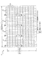
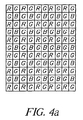
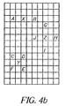
(a) アクティブイメージング画素の境界のあるアレイを形成するよう入射光を電荷へと変換する複数の感光位置と、
(b) 所定の場所において配置され、前記アクティブイメージング画素のアレイの前記境界の間に組み入れられた、1つ又はそれ以上の置換画素位置と、
を有し、
前記置換画素は、前記アクティブイメージング画素とは異なる設計であり、
前記置換画素は、前記イメージセンサの性能、動作、製造、及び/又は組立体を向上するよう、前記アクティブイメージング画素とは異なるデータ、情報、又は機能を与える、
イメージセンサ。 - 前記置換画素は、前記画素のアレイにわたって電流又は電圧の分布を向上させる増幅回路又はバッファ回路である、
請求項1記載のイメージセンサ。 - 前記置換画素は、前記画素内又は前記画素にわたって信号のインテグリティを向上させる増幅回路又はバッファ回路である、
請求項1記載のイメージセンサ。 - 前記置換画素は、他の色、赤外線構成要素、又は他の測光パラメータを有する他の画像パラメータを確定する反応特性を有する、
請求項1記載のイメージセンサ。 - 前記置換画素は、前記イメージセンサを整列するよう機構に対して使用され得る基準素子である、
請求項1記載のイメージセンサ。 - 前記置換画素は、接地接触を与える、
請求項1記載のイメージセンサ。 - 前記置換画素は、画像処理に対してオプティカルブラックレベルを与える、
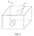
請求項1記載のイメージセンサ。 - カメラであって:
(a) イメージセンサと:
(b) 置換画素においてイメージ位置に対して信号レベルを与えることによって複数の画素が作った画像を修正する機構と、
を有し、
前記(a)イメージセンサは、
(a1) アクティブイメージング画素の境界のあるアレイを形成するよう入射光を電荷へと変換する複数の感光位置と;
(a2) 所定の場所において配置され、前記アクティブイメージング画素のアレイの前記境界の間に組み入れられた、1つ又はそれ以上の置換画素位置と;
を有し、
前記置換画素は、前記アクティブイメージング画素とは異なる設計であり、前記置換画素は、イメージング系の性能、動作、製造、及び/又は組立体を向上するよう、前記アクティブ画素とは異なるデータ、情報、及び/又は機能を与える、
カメラ。 - 前記置換画素の場所で前記信号レベルを修正して与える前記機構は、最近隣接内挿法を使用して行われる、
請求項8記載のイメージセンサ。 - カメラであって:
(a) イメージセンサを有し、
前記(a)イメージセンサは、
(a1) アクティブイメージング画素の境界のあるアレイを形成するよう入射光を電荷へと変換する複数の感光位置と;
(a2) 所定の場所において配置され、前記アクティブイメージング画素のアレイの前記境界の間に組み入れられた、1つ又はそれ以上の置換画素位置と;
を有し、
前記置換画素は、前記アクティブイメージング画素とは異なる設計であり、前記置換画素は、イメージング系の性能、動作、製造、及び/又は組立体を向上するよう、前記アクティブ画素とは異なるデータ、情報、及び/又は機能を与える、
カメラ。 - 前記置換画素は、前記画素のアレイにわたる電流又は電圧の分布を向上するよう増幅回路又はバッファ回路である、
請求項10記載のカメラ。 - 前記置換画素は、前記画素内又は前記画素にわたって信号のインテグリティを向上させる増幅回路又はバッファ回路である、
請求項10記載のカメラ。 - 前記置換画素は、他の色、赤外線構成要素、又は他の測光パラメータを有する他の画像パラメータを確定する反応特性を有する、
請求項10記載のカメラ。 - 前記置換画素は、前記イメージセンサを整列するよう機構に対して使用され得る基準素子である、
請求項10記載のカメラ。 - 前記置換画素は、接地接触を与える、
請求項10記載のカメラ。 - 前記置換画素は、画像処理に対してオプティカルブラックレベルを与える、
請求項10記載のカメラ。
Applications Claiming Priority (2)
| Application Number | Priority Date | Filing Date | Title |
|---|---|---|---|
| US10/691,047 US7304673B2 (en) | 2003-10-22 | 2003-10-22 | Image sensor array with substitutional circuit distribution |
| PCT/US2004/034324 WO2005043894A1 (en) | 2003-10-22 | 2004-10-19 | Image sensor array with substitutional circuit distribution |
Publications (2)
| Publication Number | Publication Date |
|---|---|
| JP2007509580A true JP2007509580A (ja) | 2007-04-12 |
| JP2007509580A5 JP2007509580A5 (ja) | 2007-10-18 |
Family
ID=34521786
Family Applications (1)
| Application Number | Title | Priority Date | Filing Date |
|---|---|---|---|
| JP2006536687A Pending JP2007509580A (ja) | 2003-10-22 | 2004-10-19 | 置換回路分布を有するイメージセンサアレイ |
Country Status (7)
| Country | Link |
|---|---|
| US (1) | US7304673B2 (ja) |
| EP (1) | EP1676435B1 (ja) |
| JP (1) | JP2007509580A (ja) |
| KR (1) | KR101103956B1 (ja) |
| CN (1) | CN100550994C (ja) |
| DE (1) | DE602004026462D1 (ja) |
| WO (1) | WO2005043894A1 (ja) |
Cited By (1)
| Publication number | Priority date | Publication date | Assignee | Title |
|---|---|---|---|---|
| JP2014120858A (ja) * | 2012-12-14 | 2014-06-30 | Canon Inc | 固体撮像装置 |
Families Citing this family (10)
| Publication number | Priority date | Publication date | Assignee | Title |
|---|---|---|---|---|
| JP4090984B2 (ja) * | 2003-11-14 | 2008-05-28 | 富士フイルム株式会社 | デジタルカメラ及び固体撮像装置 |
| GB2429864B (en) * | 2005-09-01 | 2008-09-24 | Micron Technology Inc | Method and apparatus providing pixel array having automatic light control pixels and image capture pixels |
| EP2132726A4 (en) * | 2007-01-16 | 2011-01-12 | Bae Systems Information | REAL-TIME PIXEL REPLACEMENT FOR THERMAL IMAGING SYSTEMS |
| US7781716B2 (en) * | 2008-03-17 | 2010-08-24 | Eastman Kodak Company | Stacked image sensor with shared diffusion regions in respective dropped pixel positions of a pixel array |
| US20110115954A1 (en) | 2009-11-19 | 2011-05-19 | Eastman Kodak Company | Sparse color pixel array with pixel substitutes |
| US8669633B2 (en) * | 2010-07-28 | 2014-03-11 | Teledyne Dalsa, Inc. | Packaged device with an image sensor aligned to a faceplate using fiducial marks and connection bodies registered thereto |
| CN102184931B (zh) * | 2011-04-19 | 2013-07-17 | 格科微电子(上海)有限公司 | 图像传感器 |
| CN102843519A (zh) * | 2011-06-23 | 2012-12-26 | 鸿富锦精密工业(深圳)有限公司 | 影像处理系统及方法 |
| JP6303352B2 (ja) * | 2013-09-18 | 2018-04-04 | 株式会社デンソーウェーブ | 外観検査システム |
| US9526468B2 (en) | 2014-09-09 | 2016-12-27 | General Electric Company | Multiple frame acquisition for exposure control in X-ray medical imagers |
Citations (2)
| Publication number | Priority date | Publication date | Assignee | Title |
|---|---|---|---|---|
| JPH0787284A (ja) * | 1993-09-17 | 1995-03-31 | Fuji Xerox Co Ltd | 2次元イメ−ジセンサ及び画素信号の補間方法 |
| JPH11126894A (ja) * | 1997-08-12 | 1999-05-11 | Hewlett Packard Co <Hp> | Cmosイメージセンサの暗電流補正方法 |
Family Cites Families (6)
| Publication number | Priority date | Publication date | Assignee | Title |
|---|---|---|---|---|
| JPH05260386A (ja) * | 1992-03-16 | 1993-10-08 | Sony Corp | 固体撮像素子の欠陥画素検出回路 |
| US6618084B1 (en) * | 1997-11-05 | 2003-09-09 | Stmicroelectronics, Inc. | Pixel correction system and method for CMOS imagers |
| US6819360B1 (en) * | 1999-04-01 | 2004-11-16 | Olympus Corporation | Image pickup element and apparatus for focusing |
| US6970193B1 (en) * | 1999-07-14 | 2005-11-29 | Olympus Optical Co., Ltd. | Electronic imaging apparatus operable in two modes with a different optical black correction procedure being effected in each mode |
| JP3922853B2 (ja) * | 1999-12-07 | 2007-05-30 | 松下電器産業株式会社 | 固体撮像装置 |
| US20030030738A1 (en) | 2001-05-22 | 2003-02-13 | Clynes Steven Derrick | On-chip 2D adjustable defective pixel filtering for CMOS imagers |
-
2003
- 2003-10-22 US US10/691,047 patent/US7304673B2/en active Active
-
2004
- 2004-10-19 WO PCT/US2004/034324 patent/WO2005043894A1/en active Application Filing
- 2004-10-19 CN CNB2004800310549A patent/CN100550994C/zh active Active
- 2004-10-19 DE DE602004026462T patent/DE602004026462D1/de active Active
- 2004-10-19 EP EP04795482A patent/EP1676435B1/en active Active
- 2004-10-19 JP JP2006536687A patent/JP2007509580A/ja active Pending
- 2004-10-19 KR KR1020067007623A patent/KR101103956B1/ko active IP Right Grant
Patent Citations (2)
| Publication number | Priority date | Publication date | Assignee | Title |
|---|---|---|---|---|
| JPH0787284A (ja) * | 1993-09-17 | 1995-03-31 | Fuji Xerox Co Ltd | 2次元イメ−ジセンサ及び画素信号の補間方法 |
| JPH11126894A (ja) * | 1997-08-12 | 1999-05-11 | Hewlett Packard Co <Hp> | Cmosイメージセンサの暗電流補正方法 |
Cited By (1)
| Publication number | Priority date | Publication date | Assignee | Title |
|---|---|---|---|---|
| JP2014120858A (ja) * | 2012-12-14 | 2014-06-30 | Canon Inc | 固体撮像装置 |
Also Published As
| Publication number | Publication date |
|---|---|
| EP1676435B1 (en) | 2010-04-07 |
| KR101103956B1 (ko) | 2012-01-13 |
| US7304673B2 (en) | 2007-12-04 |
| KR20060094524A (ko) | 2006-08-29 |
| WO2005043894A1 (en) | 2005-05-12 |
| EP1676435A1 (en) | 2006-07-05 |
| US20050088552A1 (en) | 2005-04-28 |
| CN100550994C (zh) | 2009-10-14 |
| DE602004026462D1 (de) | 2010-05-20 |
| CN1883190A (zh) | 2006-12-20 |
Similar Documents
| Publication | Publication Date | Title |
|---|---|---|
| US10136107B2 (en) | Imaging systems with visible light sensitive pixels and infrared light sensitive pixels | |
| US6646246B1 (en) | Method and system of noise removal for a sparsely sampled extended dynamic range image sensing device | |
| JP4971323B2 (ja) | カラー画素とパンクロ画素の処理 | |
| US8125543B2 (en) | Solid-state imaging device and imaging apparatus with color correction based on light sensitivity detection | |
| US8169518B2 (en) | Image pickup apparatus and signal processing method | |
| CN111757006B (zh) | 图像获取方法、摄像头组件及移动终端 | |
| US20140313350A1 (en) | Imaging systems with reference pixels for image flare mitigation | |
| US20070030365A1 (en) | Correction of cluster defects in imagers | |
| US10419664B2 (en) | Image sensors with phase detection pixels and a variable aperture | |
| US10165211B1 (en) | Image sensors with optically black pixels | |
| JP2009524988A (ja) | 光感度が改善されたイメージ・センサー | |
| JP2009504005A (ja) | 光感度が改善されたイメージ・センサー | |
| JP2016213715A (ja) | 撮像装置、撮像システム、信号処理方法 | |
| US20230086743A1 (en) | Control method, camera assembly, and mobile terminal | |
| CN110944126B (zh) | 成像系统和对图像传感器进行黑阶校正的方法 | |
| US20230140516A1 (en) | Image acquisition method, camera assembly, and mobile terminal | |
| JP4520502B2 (ja) | デジタル撮像デバイスにおける画像品質向上のための方法、装置、撮像モジュールおよびプログラム | |
| JP2007509580A (ja) | 置換回路分布を有するイメージセンサアレイ | |
| US10931902B2 (en) | Image sensors with non-rectilinear image pixel arrays | |
| US9628730B2 (en) | Dark current gradient estimation using optically black pixels | |
| US20170054925A1 (en) | Systems and methods for weighted image signal readout | |
| JP3980891B2 (ja) | 永久情報が符号化される光センサ・アレイ | |
| CN114424517B (zh) | 图像传感器、控制方法、摄像头组件及移动终端 | |
| US20220279108A1 (en) | Image sensor and mobile terminal | |
| Kumbhar et al. | Comparative study of CCD & CMOS sensors for image processing |
Legal Events
| Date | Code | Title | Description |
|---|---|---|---|
| A521 | Request for written amendment filed |
Free format text: JAPANESE INTERMEDIATE CODE: A523 Effective date: 20070828 |
|
| A621 | Written request for application examination |
Free format text: JAPANESE INTERMEDIATE CODE: A621 Effective date: 20070828 |
|
| A131 | Notification of reasons for refusal |
Free format text: JAPANESE INTERMEDIATE CODE: A131 Effective date: 20100309 |
|
| A521 | Request for written amendment filed |
Free format text: JAPANESE INTERMEDIATE CODE: A523 Effective date: 20100601 |
|
| A02 | Decision of refusal |
Free format text: JAPANESE INTERMEDIATE CODE: A02 Effective date: 20110201 |