JP2007328900A - Static semiconductor memory - Google Patents
Static semiconductor memory Download PDFInfo
- Publication number
- JP2007328900A JP2007328900A JP2007028839A JP2007028839A JP2007328900A JP 2007328900 A JP2007328900 A JP 2007328900A JP 2007028839 A JP2007028839 A JP 2007028839A JP 2007028839 A JP2007028839 A JP 2007028839A JP 2007328900 A JP2007328900 A JP 2007328900A
- Authority
- JP
- Japan
- Prior art keywords
- channel mos
- memory cell
- pair
- transistors
- dummy
- Prior art date
- Legal status (The legal status is an assumption and is not a legal conclusion. Google has not performed a legal analysis and makes no representation as to the accuracy of the status listed.)
- Withdrawn
Links
Images


Classifications
-
- G—PHYSICS
- G11—INFORMATION STORAGE
- G11C—STATIC STORES
- G11C11/00—Digital stores characterised by the use of particular electric or magnetic storage elements; Storage elements therefor
- G11C11/21—Digital stores characterised by the use of particular electric or magnetic storage elements; Storage elements therefor using electric elements
- G11C11/34—Digital stores characterised by the use of particular electric or magnetic storage elements; Storage elements therefor using electric elements using semiconductor devices
- G11C11/40—Digital stores characterised by the use of particular electric or magnetic storage elements; Storage elements therefor using electric elements using semiconductor devices using transistors
- G11C11/41—Digital stores characterised by the use of particular electric or magnetic storage elements; Storage elements therefor using electric elements using semiconductor devices using transistors forming static cells with positive feedback, i.e. cells not needing refreshing or charge regeneration, e.g. bistable multivibrator or Schmitt trigger
- G11C11/412—Digital stores characterised by the use of particular electric or magnetic storage elements; Storage elements therefor using electric elements using semiconductor devices using transistors forming static cells with positive feedback, i.e. cells not needing refreshing or charge regeneration, e.g. bistable multivibrator or Schmitt trigger using field-effect transistors only
-
- G—PHYSICS
- G11—INFORMATION STORAGE
- G11C—STATIC STORES
- G11C11/00—Digital stores characterised by the use of particular electric or magnetic storage elements; Storage elements therefor
- G11C11/21—Digital stores characterised by the use of particular electric or magnetic storage elements; Storage elements therefor using electric elements
- G11C11/34—Digital stores characterised by the use of particular electric or magnetic storage elements; Storage elements therefor using electric elements using semiconductor devices
- G11C11/40—Digital stores characterised by the use of particular electric or magnetic storage elements; Storage elements therefor using electric elements using semiconductor devices using transistors
- G11C11/41—Digital stores characterised by the use of particular electric or magnetic storage elements; Storage elements therefor using electric elements using semiconductor devices using transistors forming static cells with positive feedback, i.e. cells not needing refreshing or charge regeneration, e.g. bistable multivibrator or Schmitt trigger
- G11C11/413—Auxiliary circuits, e.g. for addressing, decoding, driving, writing, sensing, timing or power reduction
Abstract
Description
本発明は、スタティック型半導体記憶装置の信頼性向上、高速化、低消費電力化の技術に関するものである。 The present invention relates to a technology for improving the reliability, speeding up, and reducing power consumption of a static semiconductor memory device.
各々6トランジスタ構成の多数のメモリセルを有するCMOS(complementary metal oxide semiconductor)型のSRAM(static random access memory)が知られている。各メモリセルは、1対のPチャネルMOS負荷トランジスタと、1対のNチャネルMOS転送トランジスタと、1対のNチャネルMOS駆動トランジスタとで構成される。 A complementary metal oxide semiconductor (SRAM) type static random access memory (SRAM) having a large number of memory cells each having six transistors is known. Each memory cell includes a pair of P-channel MOS load transistors, a pair of N-channel MOS transfer transistors, and a pair of N-channel MOS drive transistors.
近年、電源電圧の低下や、トランジスタサイズのシュリンクに伴い、メモリセルを構成する各トランジスタの能力が低下傾向にあり、書き込み速度が遅くなってきている。この対策として、メモリセルへのデータの書き込み動作時に、この書き込み動作の補助をする技術が種々提案されている。例えば、書き込みサイクルの間だけメモリセル中の1対のPチャネルMOS負荷トランジスタ用のソース電源を降圧するように、当該PチャネルMOS負荷トランジスタのソースをフローティングにするという書き込み補助技術が知られている(非特許文献1参照)。
従来のSRAMでは、ワースト条件で正常書き込みを保証するように、書き込み補助のために例えば負荷トランジスタ用ソース電源をどの程度降圧するのかや、書き込み補助動作を実行する期間の長さが、一定のマージンを見込んで予めシミュレーションにより決定されていた。このマージンが大きすぎると、電圧を通常状態に戻すのに要する充放電電流分の消費電力が無駄に必要になったり、電圧を通常状態に戻すためのドライバのサイズを余分に大きくすることが必要になったりする。また、書き込み補助動作がデータを書き込まないメモリセルのリテンションに影響する場合には、信頼性の低下に繋がる。 In a conventional SRAM, in order to guarantee normal writing under the worst condition, for example, how much the source power for the load transistor is stepped down for writing assistance, and the length of the period during which the writing assistance operation is performed has a certain margin. Was determined by simulation in advance. If this margin is too large, the power consumption required to return the voltage to the normal state is wasted, or the driver size for returning the voltage to the normal state must be increased. It becomes. Further, when the write assist operation affects the retention of the memory cell to which data is not written, the reliability is lowered.
本発明の目的は、スタティック型半導体記憶装置における書き込み動作の確実性を保証する電源及び基板電位の制御技術を提供することにある。 An object of the present invention is to provide a power supply and substrate potential control technique that guarantees the reliability of a write operation in a static semiconductor memory device.
上記課題を解決するため、本発明によれば、書き込み完了タイミング検出用のダミーメモリセルをメモリセルのレプリカとして設け、メモリセルの電源制御及び基板電位制御により書き込み動作の補助を行う際に、ダミーメモリセルの情報をもとに書き込み補助動作の終了タイミングを決定する。 In order to solve the above problems, according to the present invention, dummy memory cells for detecting write completion timing are provided as replicas of memory cells, and dummy operation is performed when assisting a write operation by controlling power supply and substrate potential of the memory cells. The end timing of the write assist operation is determined based on the memory cell information.
具体的に説明すると、本発明によれば、メモリセルへのデータ書き込み動作時に、メモリセル及びダミーメモリセルの双方のPチャネルMOS負荷トランジスタ用のソース電源を降圧する書き込み補助動作と、メモリセル及びダミーメモリセルの双方のNチャネルMOS駆動トランジスタ用のソース電源を昇圧する書き込み補助動作と、メモリセル及びダミーメモリセルの双方のPチャネルMOS負荷トランジスタの基板電位を上げる書き込み補助動作と、メモリセル及びダミーメモリセルの双方のNチャネルMOS転送トランジスタの基板電位を上げる書き込み補助動作と、メモリセル及びダミーメモリセルの双方のNチャネルMOS駆動トランジスタの基板電位を下げる書き込み補助動作とのうち少なくとも1つの書き込み補助動作を行った後、ダミーメモリセルへのデータ書き込み動作の完了を検知した時点で書き込み補助動作を終了する。 More specifically, according to the present invention, during a data write operation to a memory cell, a write assist operation for stepping down the source power supply for the P-channel MOS load transistors of both the memory cell and the dummy memory cell, A write assist operation for boosting the source power supply for both N-channel MOS drive transistors of the dummy memory cell, a write assist operation for raising the substrate potential of the P-channel MOS load transistors of both the memory cell and the dummy memory cell, At least one of the write assist operation for increasing the substrate potential of the N channel MOS transfer transistors of both the dummy memory cells and the write assist operation for decreasing the substrate potential of the N channel MOS drive transistors of both the memory cells and the dummy memory cells. Perform auxiliary action After terminates the write assist operation when it detects the completion of the data write operation to the dummy memory cell.
PチャネルMOS負荷トランジスタ用ソース電源を降圧する動作、又はPチャネルMOS負荷トランジスタ基板電位を上げる動作を実行すれば、メモリセル中のPチャネルMOS負荷トランジスタの電流が減少するため、当該メモリセルの2つの記憶ノードを書き込み前の状態に保持する能力が低下する結果、書き込み動作の確実性が向上する。 If the operation of stepping down the source power supply for the P-channel MOS load transistor or the operation of raising the P-channel MOS load transistor substrate potential is performed, the current of the P-channel MOS load transistor in the memory cell is decreased. As a result of the reduced ability to hold one storage node in the state prior to writing, the certainty of the write operation is improved.
NチャネルMOS転送トランジスタ基板電位を上げる動作を実行すれば、メモリセル中のNチャネルMOS転送トランジスタの電流が増加するため、当該メモリセルの2つの記憶ノードにデータを書き込む能力が向上する結果、書き込み動作の確実性が向上する。 If the operation for raising the substrate potential of the N channel MOS transfer transistor is executed, the current of the N channel MOS transfer transistor in the memory cell increases, so that the ability to write data to the two storage nodes of the memory cell is improved. The certainty of operation is improved.
NチャネルMOS駆動トランジスタ用ソース電源を昇圧する動作、又はNチャネルMOS駆動トランジスタ基板電位を下げる動作を実行すれば、メモリセル中のNチャネルMOS駆動トランジスタの電流が減少するため、当該メモリセルの2つの記憶ノードを書き込み前の状態に保持する能力が低下する結果、書き込み動作の確実性が向上する。 If the operation of boosting the source power supply for the N channel MOS drive transistor or the operation of lowering the N channel MOS drive transistor substrate potential is performed, the current of the N channel MOS drive transistor in the memory cell is decreased. As a result of the reduced ability to hold one storage node in the state prior to writing, the certainty of the write operation is improved.
しかも、本発明によれば、ダミーメモリセルへのデータ書き込み動作の完了を検知した時点で書き込み補助動作を終了することとしたので、書き込み動作の補助に必要な最小限の電圧調整幅が得られる。 In addition, according to the present invention, since the write assist operation is terminated when the completion of the data write operation to the dummy memory cell is detected, the minimum voltage adjustment width necessary for assisting the write operation can be obtained. .
本明によれば、書き込み動作の補助に必要な最小限の電圧調整幅が得られるため、書き込み動作の安定性を高め、かつ低消費電力化、データ保持特性の向上を実現できる。 According to the present invention, since the minimum voltage adjustment width necessary for assisting the write operation can be obtained, it is possible to improve the stability of the write operation, reduce the power consumption, and improve the data retention characteristics.
以下、図1〜図4を用いて、本発明の実施形態を詳細に説明する。 Hereinafter, embodiments of the present invention will be described in detail with reference to FIGS.
図1は、本発明に係るスタティック型半導体記憶装置の構成例を示している。図1において、10はメモリセル、20はダミーメモリセル、30は電圧制御回路である。 FIG. 1 shows a configuration example of a static type semiconductor memory device according to the present invention. In FIG. 1, 10 is a memory cell, 20 is a dummy memory cell, and 30 is a voltage control circuit.
メモリセル10は、6トランジスタ構成のSRAMメモリセルであって、1対のPチャネルMOS負荷トランジスタ11と、1対のNチャネルMOS転送トランジスタ12と、1対のNチャネルMOS駆動トランジスタ13とを有する。一方のPチャネルMOS負荷トランジスタ11のドレインと一方のNチャネルMOS駆動トランジスタ13のドレインとの接続点が第1の記憶ノードを、他方のPチャネルMOS負荷トランジスタ11のドレインと他方のNチャネルMOS駆動トランジスタ13のドレインとの接続点が第2の記憶ノードをそれぞれ構成する。第1の記憶ノードは一方のNチャネルMOS転送トランジスタ12を介して一方のビット線14に、第2の記憶ノードは他方のNチャネルMOS転送トランジスタ12を介して他方のビット線15にそれぞれ接続されている。両NチャネルMOS転送トランジスタ12の各々のゲートは、ワード線100に接続されている。両PチャネルMOS負荷トランジスタ11の各々のソースはPチャネルMOS負荷トランジスタ用ソース電源101に、両NチャネルMOS駆動トランジスタ13の各々のソースはNチャネルMOS駆動トランジスタ用ソース電源105にそれぞれ接続されている。また、両PチャネルMOS負荷トランジスタ11の各々のバックゲートはPチャネルMOS負荷トランジスタ基板電位104に、両NチャネルMOS転送トランジスタ12の各々のバックゲートはNチャネルMOS転送トランジスタ基板電位103に、両NチャネルMOS駆動トランジスタ13の各々のバックゲートはNチャネルMOS駆動トランジスタ基板電位102にそれぞれ接続されている。1対のビット線14,15に任意の相補データ信号を供給しつつ、ワード線100をHレベルに設定することにより両NチャネルMOS転送トランジスタ12を導通させれば、当該メモリセル10に任意のデータを書き込むことができる。
The
ダミーメモリセル20は、メモリセル10のレプリカとして設けられたものであって、メモリセル10と同様に、1対のPチャネルMOS負荷トランジスタ21と、1対のNチャネルMOS転送トランジスタ22と、1対のNチャネルMOS駆動トランジスタ23とを有する。一方のPチャネルMOS負荷トランジスタ21のドレインと一方のNチャネルMOS駆動トランジスタ23のドレインとの接続点が第1の記憶ノード4を、他方のPチャネルMOS負荷トランジスタ21のドレインと他方のNチャネルMOS駆動トランジスタ23のドレインとの接続点が第2の記憶ノード5をそれぞれ構成する。第1の記憶ノード4は一方のNチャネルMOS転送トランジスタ22を介して一方のダミービット線24に、第2の記憶ノード5は他方のNチャネルMOS転送トランジスタ22を介して他方のダミービット線25にそれぞれ接続されている。両NチャネルMOS転送トランジスタ22の各々のゲートは、前記ワード線100に接続されている。両PチャネルMOS負荷トランジスタ21の各々のソースは前記PチャネルMOS負荷トランジスタ用ソース電源101に、両NチャネルMOS駆動トランジスタ23の各々のソースは前記NチャネルMOS駆動トランジスタ用ソース電源105にそれぞれ接続されている。また、両PチャネルMOS負荷トランジスタ21の各々のバックゲートは前記PチャネルMOS負荷トランジスタ基板電位104に、両NチャネルMOS転送トランジスタ22の各々のバックゲートは前記NチャネルMOS転送トランジスタ基板電位103に、両NチャネルMOS駆動トランジスタ23の各々のバックゲートは前記NチャネルMOS駆動トランジスタ基板電位102にそれぞれ接続されている。
The
電圧制御回路30は、メモリセル10へのデータ書き込み動作時に、PチャネルMOS負荷トランジスタ用ソース電源101を降圧する書き込み補助動作を行った後、ダミーメモリセル20へのデータ書き込み動作の完了を検知した時点で書き込み補助動作を終了するように制御する回路であって、第1のANDゲート31と、PチャネルMOSリセットトランジスタ32と、NチャネルMOS電位設定トランジスタ33と、PチャネルMOS電位設定トランジスタ34と、第2のANDゲート35と、インバータ回路36と、PチャネルMOSプルダウントランジスタ37と、PチャネルMOSプルアップトランジスタ38とを有する。
The
第1のANDゲート31は、クロック信号200と書き込みイネーブル信号201とを受け取り、その出力をPチャネルMOSリセットトランジスタ32のゲートと、NチャネルMOS電位設定トランジスタ33のゲートと、第2のANDゲート35の第1入力とに供給する。
The first AND
PチャネルMOSリセットトランジスタ32は、メモリセル10へのデータ書き込み前に、すなわち第1のANDゲート31の出力がLレベルである間に導通して、ダミーメモリセル20の第2の記憶ノード5をHレベルにリセットするためのトランジスタである。この際、当該ダミーメモリセル20の第1の記憶ノード4は自動的にLレベルにリセットされる。
The P-channel
NチャネルMOS電位設定トランジスタ33は、メモリセル10へのデータ書き込み動作が開始した時点から、すなわち第1のANDゲート31の出力がLレベルからHレベルへ遷移した時点から導通して、一方のダミービット線25の電位をLレベルに設定する。PチャネルMOS電位設定トランジスタ34は、当該ダミービット線25の電位がLレベルに設定された時点から導通して、他方のダミービット線24の電位をHレベルに設定する。つまり、これらの電位設定トランジスタ33,34は、第1及び第2の記憶ノード4,5のリセットされた電位を各々反転させるように、ダミーメモリセル20に書き込むべき所定のダミーデータを供給するものである。
The N channel MOS
第2のANDゲート35は、ダミーメモリセル20の第2の記憶ノード5の電位を第2入力として受け取り、その出力をインバータ回路36の入力と、PチャネルMOSプルアップトランジスタ38のゲートとに供給する。インバータ回路36は、第2のANDゲート35の出力を反転した信号をPチャネルMOSプルダウントランジスタ37のゲートに供給する。
The second AND
この結果、電圧制御回路30は、通常はPチャネルMOSプルアップトランジスタ38が導通してPチャネルMOS負荷トランジスタ用ソース電源101を高い電圧に保持し、メモリセル10へのデータ書き込み動作が開始して第2のANDゲート35の出力がHレベルになるとPチャネルMOSプルダウントランジスタ37が導通してPチャネルMOS負荷トランジスタ用ソース電源101を降圧する書き込み補助動作を開始し、ダミーメモリセル20へのデータ書き込み動作が完了して第2の記憶ノード5の電位がLレベルになると書き込み補助動作を終了してPチャネルMOSプルアップトランジスタ38が再度導通することによりPチャネルMOS負荷トランジスタ用ソース電源101を元の電圧に戻すように動作する。
As a result, normally, the P-channel MOS pull-
以上のとおり、図1のスタティック型半導体記憶装置によれば、書き込み完了タイミング検出用のダミーメモリセル20をメモリセル10のレプリカとして設け、PチャネルMOS負荷トランジスタ用ソース電源101を降圧する書き込み補助動作を行う際に、ダミーメモリセル20の第2の記憶ノード5の電位をもとに書き込み補助動作の終了タイミングを決定することとしたので、書き込み動作の補助に必要な最小限の電圧調整幅が得られる。この結果、書き込み動作の安定性を高め、かつ低消費電力化、データ保持特性の向上を実現できる。
As described above, according to the static semiconductor memory device of FIG. 1, the write assist operation for providing the
図2は、本発明に係るスタティック型半導体記憶装置の他の構成例を示している。図2によれば、第1及び第2のダミーメモリセル20a,20bがそれぞれメモリセル10のレプリカとして設けられる。24a及び25aは第1のダミーメモリセル20aの1対のダミービット線であり、24b及び25bは第2のダミーメモリセル20bの1対のダミービット線である。電圧制御回路30は、第1及び第2のダミーメモリセル20a,20bへのデータ書き込み動作の完了を示す2つの信号に応答して、PチャネルMOS負荷トランジスタ用ソース電源101を降圧する書き込み補助動作の終了タイミングを決定するように構成されている。具体的に説明すると、32a及び32bはPチャネルMOSリセットトランジスタ、33a及び33bはNチャネルMOS電位設定トランジスタ、34a及び34bはPチャネルMOS電位設定トランジスタであり、第2のANDゲート35は、第1のANDゲート31の出力と、第1のダミーメモリセル20aへのデータ書き込み動作の完了を示す信号と、第2のダミーメモリセル20bへのデータ書き込み動作の完了を示す信号とを受け取る3入力ゲートである。
FIG. 2 shows another configuration example of the static semiconductor memory device according to the present invention. According to FIG. 2, first and second
図2のスタティック型半導体記憶装置では、第1及び第2のダミーメモリセル20a,20bへのデータ書き込み動作の完了を示す2つの信号の論理積に基づいて、第2のANDゲート35にて書き込み補助動作の終了タイミングを決定する。メモリセル10並びに第1及び第2のダミーメモリセル20a,20bの書き込み特性にはばらつきがあるが、第1及び第2のダミーメモリセル20a,20bのうち遅くデータ書き込み動作が完了するダミーメモリセルの特性に従って書き込み補助動作の終了タイミングが決定されるので、メモリセル10の書き込み動作の確実性が向上する。
In the static semiconductor memory device of FIG. 2, writing is performed by the second AND
なお、第1及び第2のダミーメモリセル20a,20bへのデータ書き込み動作の完了を示す2つの信号の論理和に基づいて書き込み補助動作の終了タイミングを決定することとしてもよい。また、3個以上のダミーメモリセルをメモリセル10のレプリカとして設けてもよい。使用するダミーメモリセルの数を動的に変更することも可能である。
Note that the end timing of the write assist operation may be determined based on the logical sum of two signals indicating the completion of the data write operation to the first and second
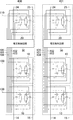
図3は、本発明に係るスタティック型半導体記憶装置の更に他の構成例を示している。図3によれば、1本のワード線100を共有する複数のメモリセル10が第1のワード300を構成し、他の1本のワード線100を共有する複数のメモリセル10が第2のワード301を構成する。第1のワード300と第2のワード301との間で電源系統が分離されており、ワード毎にダミーメモリセル20と電圧制御回路30とが設けられる。ワード毎の電圧制御回路30は、ダミーメモリセル20を利用して複数のメモリセル10の各々に同じ書き込み補助動作を行う。ここに、書き込み補助動作とは、PチャネルMOS負荷トランジスタ用ソース電源101を降圧する動作と、NチャネルMOS駆動トランジスタ用ソース電源105を昇圧する動作と、PチャネルMOS負荷トランジスタ基板電位104を上げる動作と、NチャネルMOS転送トランジスタ基板電位103を上げる動作と、NチャネルMOS駆動トランジスタ基板電位102を下げる動作とのうち少なくとも1つの動作をいう。電圧制御回路30は、メモリセル10へのデータ書き込み動作時に、ダミーメモリセル20へのデータ書き込み動作の完了を検知した時点で書き込み補助動作を終了するように制御する。
FIG. 3 shows still another configuration example of the static semiconductor memory device according to the present invention. According to FIG. 3, a plurality of
図3によれば、ワード毎に独立した電圧制御回路30を設けたので、書き込み補助動作がデータを書き込まないワード(非選択ワード)中のメモリセル10のリテンションに悪影響を及ぼすことがない。複数のダミーメモリセルをワード毎に設けてもよい。
According to FIG. 3, since the independent
図4は、本発明に係るスタティック型半導体記憶装置の更に他の構成例を示している。図4によれば、1対のビット線14,15を共有する複数のメモリセル10が第1のビット400を構成し、他の1対のビット線14,15を共有する複数のメモリセル10が第2のビット401を構成する。第1のビット400と第2のビット401との間で電源系統が分離されており、ビット毎にダミーメモリセル20と電圧制御回路30とが設けられる。110はダミーワード線である。ビット毎の電圧制御回路30は、複数のメモリセル10の各々に同じ書き込み補助動作を行い、ダミーメモリセル20へのデータ書き込み動作の完了を検知した時点で書き込み補助動作を終了するように制御する。
FIG. 4 shows still another configuration example of the static semiconductor memory device according to the present invention. According to FIG. 4, a plurality of
図4によれば、ビット毎に独立した電圧制御回路30を設けたので、書き込み補助動作がデータを書き込まないビット(非選択ビット)中のメモリセル10のリテンションに悪影響を及ぼすことがない。複数のダミーメモリセルをビット毎に設けてもよい。複数ビットからなるブロック毎に1つの電圧制御回路30と、1又は複数のダミーメモリセルとを設けてもよい。
According to FIG. 4, since an independent
以上、図1〜図4を用いて本発明の実施形態を説明したが、種々の変形が可能である。例えば、図1中のダミーメモリセル20の1対のNチャネルMOS駆動トランジスタ23の各々のソース電源を別々に制御することにより、ダミーメモリセル20の第1及び第2の記憶ノード4,5をリセットすることも可能である。メモリセル10中のNチャネルMOS転送トランジスタ12のゲートに与える選択信号に先んじて、ダミーメモリセル20中のNチャネルMOS転送トランジスタ22のゲートにダミー選択信号を与えるようにしてもよい。ダミーメモリセル20中に流れる電流をもとに当該ダミーメモリセル20へのデータ書き込み動作の完了を検知することもできる。
As mentioned above, although embodiment of this invention was described using FIGS. 1-4, a various deformation | transformation is possible. For example, the first and
また、ダミーメモリセル20において、PチャネルMOS負荷トランジスタ21のソース電源、NチャネルMOS駆動トランジスタ23のソース電源、PチャネルMOS負荷トランジスタ21の閾値、NチャネルMOS転送トランジスタ22の閾値、NチャネルMOS駆動トランジスタ23の閾値のうちいずれかを調整することにより、電圧制御回路30の動作タイミングを調整することも可能である。
In the
また、電圧制御回路30における書き込み補助動作の開始タイミング及び終了タイミングを外部信号に応じて調整できるようにしてもよい。電圧制御回路30による書き込み補助動作を外部信号に応じて禁止することも可能である。
Further, the start timing and end timing of the write assist operation in the
以上説明してきたとおり、本発明に係るスタティック型半導体記憶装置は、書き込み完了タイミング検出用のダミーメモリセルをメモリセルのレプリカとして設け、ダミーメモリセルの情報をもとにメモリセルの書き込み補助動作の終了タイミングを決定することとしたので、書き込み動作の安定性を高め、かつ低消費電力化、データ保持特性の向上を実現でき、いわゆるSRAM等として有用である。 As described above, in the static semiconductor memory device according to the present invention, the dummy memory cell for detecting the write completion timing is provided as a replica of the memory cell, and the memory cell write assist operation is performed based on the information of the dummy memory cell. Since the end timing is determined, the stability of the write operation can be improved, power consumption can be reduced, and data retention characteristics can be improved, which is useful as a so-called SRAM or the like.
4,5 ダミーメモリセルの記憶ノード
10 メモリセル
11 PチャネルMOS負荷トランジスタ
12 NチャネルMOS転送トランジスタ
13 NチャネルMOS駆動トランジスタ
14,15 ビット線
20,20a,20b ダミーメモリセル
21 PチャネルMOS負荷トランジスタ
22 NチャネルMOS転送トランジスタ
23 NチャネルMOS駆動トランジスタ
24,25 ダミービット線
24a,25a ダミービット線
24b,25b ダミービット線
30 電圧制御回路
31,35 ANDゲート
32,32a,32b PチャネルMOSリセットトランジスタ
33,33a,33b NチャネルMOS電位設定トランジスタ
34,34a,34b PチャネルMOS電位設定トランジスタ
36 インバータ回路
37 PチャネルMOSプルダウントランジスタ
38 PチャネルMOSプルアップトランジスタ
100 ワード線
101 PチャネルMOS負荷トランジスタ用ソース電源
102 NチャネルMOS駆動トランジスタ基板電位
103 NチャネルMOS転送トランジスタ基板電位
104 PチャネルMOS負荷トランジスタ基板電位
105 NチャネルMOS駆動トランジスタ用ソース電源
110 ダミーワード線
200 クロック信号
201 書き込みイネーブル信号
300,301 ワード
400,401 ビット
4, 5
Claims (4)
1対のPチャネルMOS負荷トランジスタと、1対のNチャネルMOS転送トランジスタと、1対のNチャネルMOS駆動トランジスタとを有するダミーメモリセルと、
前記メモリセルへのデータ書き込み動作時に、前記メモリセル及び前記ダミーメモリセルの双方の前記PチャネルMOS負荷トランジスタ用のソース電源を降圧する書き込み補助動作と、前記メモリセル及び前記ダミーメモリセルの双方の前記NチャネルMOS駆動トランジスタ用のソース電源を昇圧する書き込み補助動作と、前記メモリセル及び前記ダミーメモリセルの双方の前記PチャネルMOS負荷トランジスタの基板電位を上げる書き込み補助動作と、前記メモリセル及び前記ダミーメモリセルの双方の前記NチャネルMOS転送トランジスタの基板電位を上げる書き込み補助動作と、前記メモリセル及び前記ダミーメモリセルの双方の前記NチャネルMOS駆動トランジスタの基板電位を下げる書き込み補助動作とのうち少なくとも1つの書き込み補助動作を行った後、前記ダミーメモリセルへのデータ書き込み動作の完了を検知した時点で前記書き込み補助動作を終了するように制御する電圧制御回路とを備えたことを特徴とするスタティック型半導体記憶装置。 A memory cell having a pair of P-channel MOS load transistors, a pair of N-channel MOS transfer transistors, and a pair of N-channel MOS drive transistors;
A dummy memory cell having a pair of P-channel MOS load transistors, a pair of N-channel MOS transfer transistors, and a pair of N-channel MOS drive transistors;
During a data write operation to the memory cell, a write assist operation for stepping down the source power supply for the P-channel MOS load transistor of both the memory cell and the dummy memory cell, and both of the memory cell and the dummy memory cell A write assist operation for boosting the source power supply for the N channel MOS drive transistor, a write assist operation for raising the substrate potential of the P channel MOS load transistor of both the memory cell and the dummy memory cell, the memory cell, and the memory cell A write assist operation for increasing the substrate potential of the N-channel MOS transfer transistors in both of the dummy memory cells, and a write assist operation for decreasing the substrate potential of the N-channel MOS drive transistors in both the memory cells and the dummy memory cells. At least A static voltage control circuit comprising: a voltage control circuit that controls to end the write assist operation when it detects completion of a data write operation to the dummy memory cell after performing one write assist operation. Type semiconductor memory device.
1対のPチャネルMOS負荷トランジスタと、1対のNチャネルMOS転送トランジスタと、1対のNチャネルMOS駆動トランジスタとを有する他のダミーメモリセルを更に備え、
前記電圧制御回路は、前記複数のダミーメモリセルの各々へのデータ書き込み動作の完了を示す複数の信号の論理演算結果に基づいて前記書き込み補助動作の終了タイミングを決定することを特徴とするスタティック型半導体記憶装置。 The static semiconductor memory device according to claim 1,
And further comprising another dummy memory cell having a pair of P-channel MOS load transistors, a pair of N-channel MOS transfer transistors, and a pair of N-channel MOS drive transistors,
The static voltage control circuit determines an end timing of the write assist operation based on a logical operation result of a plurality of signals indicating completion of a data write operation to each of the plurality of dummy memory cells. Semiconductor memory device.
1対のPチャネルMOS負荷トランジスタと、1対のNチャネルMOS転送トランジスタと、1対のNチャネルMOS駆動トランジスタとを有し、かつ1本のワード線を前記メモリセルと共有する他のメモリセルを更に備え、
前記電圧制御回路は、前記ダミーメモリセルを利用して前記複数のメモリセルの各々に同じ書き込み補助動作を行うことを特徴とするスタティック型半導体記憶装置。 The static semiconductor memory device according to claim 1,
Another memory cell having a pair of P-channel MOS load transistors, a pair of N-channel MOS transfer transistors, and a pair of N-channel MOS driving transistors, and sharing one word line with the memory cell Further comprising
2. The static semiconductor memory device according to claim 1, wherein the voltage control circuit performs the same write assist operation on each of the plurality of memory cells using the dummy memory cell.
1対のPチャネルMOS負荷トランジスタと、1対のNチャネルMOS転送トランジスタと、1対のNチャネルMOS駆動トランジスタとを有し、かつ1対のビット線を前記メモリセルと共有する他のメモリセルを更に備え、
前記電圧制御回路は、前記ダミーメモリセルを利用して前記複数のメモリセルの各々に同じ書き込み補助動作を行うことを特徴とするスタティック型半導体記憶装置。 The static semiconductor memory device according to claim 1,
Another memory cell having a pair of P-channel MOS load transistors, a pair of N-channel MOS transfer transistors, a pair of N-channel MOS drive transistors, and sharing a pair of bit lines with the memory cell Further comprising
2. The static semiconductor memory device according to claim 1, wherein the voltage control circuit performs the same write assist operation on each of the plurality of memory cells using the dummy memory cell.
Priority Applications (2)
| Application Number | Priority Date | Filing Date | Title |
|---|---|---|---|
| JP2007028839A JP2007328900A (en) | 2006-05-09 | 2007-02-08 | Static semiconductor memory |
| US11/730,977 US7978503B2 (en) | 2006-05-09 | 2007-04-05 | Static semiconductor memory with a dummy call and a write assist operation |
Applications Claiming Priority (2)
| Application Number | Priority Date | Filing Date | Title |
|---|---|---|---|
| JP2006129832 | 2006-05-09 | ||
| JP2007028839A JP2007328900A (en) | 2006-05-09 | 2007-02-08 | Static semiconductor memory |
Publications (2)
| Publication Number | Publication Date |
|---|---|
| JP2007328900A true JP2007328900A (en) | 2007-12-20 |
| JP2007328900A5 JP2007328900A5 (en) | 2010-02-25 |
Family
ID=38684937
Family Applications (1)
| Application Number | Title | Priority Date | Filing Date |
|---|---|---|---|
| JP2007028839A Withdrawn JP2007328900A (en) | 2006-05-09 | 2007-02-08 | Static semiconductor memory |
Country Status (2)
| Country | Link |
|---|---|
| US (1) | US7978503B2 (en) |
| JP (1) | JP2007328900A (en) |
Cited By (3)
| Publication number | Priority date | Publication date | Assignee | Title |
|---|---|---|---|---|
| US7978559B2 (en) | 2008-09-08 | 2011-07-12 | Samsung Electronics Co., Ltd. | Semiconductor memory device and method of operating the same |
| US8451672B2 (en) | 2010-07-07 | 2013-05-28 | Kabushiki Kaisha Toshiba | Semiconductor storage device |
| US8730712B2 (en) | 2010-12-29 | 2014-05-20 | Samsung Electronics Co., Ltd. | SRAM including write assist circuit and method of operating same |
Families Citing this family (16)
| Publication number | Priority date | Publication date | Assignee | Title |
|---|---|---|---|---|
| US7376032B2 (en) * | 2006-06-01 | 2008-05-20 | Qualcomm Incorporated | Method and apparatus for a dummy SRAM cell |
| US7630264B2 (en) * | 2007-07-24 | 2009-12-08 | Infineon Technologies Ag | Memory device and testing with write completion detection |
| US20090285039A1 (en) * | 2008-05-15 | 2009-11-19 | International Business Machines Corporation | Method and apparatus for locally generating a virtual ground for write assist on column selected sram cells |
| US7817481B2 (en) * | 2008-07-03 | 2010-10-19 | International Business Machines Corporation | Column selectable self-biasing virtual voltages for SRAM write assist |
| KR20100028416A (en) * | 2008-09-04 | 2010-03-12 | 삼성전자주식회사 | Semiconductor memory device, method of operating the same |
| KR101446337B1 (en) | 2008-09-08 | 2014-10-02 | 삼성전자주식회사 | Semiconductor Memory Device, Method of Operating the same |
| US8111579B2 (en) * | 2008-11-10 | 2012-02-07 | Intel Corporation | Circuits and methods for reducing minimum supply for register file cells |
| US9093176B2 (en) * | 2012-11-12 | 2015-07-28 | Taiwan Semiconductor Manufacturing Co., Ltd. | Power line lowering for write assisted control scheme |
| JP6269509B2 (en) * | 2013-01-21 | 2018-01-31 | 株式会社ソシオネクスト | CAM cell for overwriting comparison data during mask operation |
| US20140293679A1 (en) * | 2013-03-26 | 2014-10-02 | International Business Machines Corporation | Management of sram initialization |
| US9299419B1 (en) | 2015-02-02 | 2016-03-29 | Qualcomm Incorporated | System and method for dynamically adjusting memory rail voltage |
| US10163524B2 (en) | 2016-06-22 | 2018-12-25 | Darryl G. Walker | Testing a semiconductor device including a voltage detection circuit and temperature detection circuit that can be used to generate read assist and/or write assist in an SRAM circuit portion and method therefor |
| US10049727B2 (en) | 2016-06-22 | 2018-08-14 | Darryl G. Walker | Semiconductor devices, circuits and methods for read and/or write assist of an SRAM circuit portion based on voltage detection and/or temperature detection circuits |
| CN109308920B (en) * | 2017-07-27 | 2020-11-13 | 中芯国际集成电路制造(上海)有限公司 | Power supply control circuit for static random access memory array |
| KR20220061772A (en) * | 2020-11-06 | 2022-05-13 | 삼성전자주식회사 | Integrated circuit including cell array with write assist cells |
| US11955171B2 (en) | 2021-09-15 | 2024-04-09 | Mavagail Technology, LLC | Integrated circuit device including an SRAM portion having end power select circuits |
Family Cites Families (8)
| Publication number | Priority date | Publication date | Assignee | Title |
|---|---|---|---|---|
| US5793671A (en) | 1997-01-21 | 1998-08-11 | Advanced Micro Devices, Inc. | Static random access memory cell utilizing enhancement mode N-channel transistors as load elements |
| US6201757B1 (en) * | 1998-08-20 | 2001-03-13 | Texas Instruments Incorporated | Self-timed memory reset circuitry |
| JP2001143476A (en) | 1999-11-15 | 2001-05-25 | Mitsubishi Electric Corp | Static semiconductor memory |
| JP2002042476A (en) | 2000-07-25 | 2002-02-08 | Mitsubishi Electric Corp | Static semiconductor memory |
| US6363005B1 (en) * | 2001-03-07 | 2002-03-26 | United Microelectronics Corp. | Method of increasing operating speed of SRAM |
| JP4162076B2 (en) | 2002-05-30 | 2008-10-08 | 株式会社ルネサステクノロジ | Semiconductor memory device |
| JP4090967B2 (en) * | 2003-08-29 | 2008-05-28 | 松下電器産業株式会社 | Semiconductor memory device |
| JP4050690B2 (en) * | 2003-11-21 | 2008-02-20 | 株式会社東芝 | Semiconductor integrated circuit device |
-
2007
- 2007-02-08 JP JP2007028839A patent/JP2007328900A/en not_active Withdrawn
- 2007-04-05 US US11/730,977 patent/US7978503B2/en not_active Expired - Fee Related
Cited By (3)
| Publication number | Priority date | Publication date | Assignee | Title |
|---|---|---|---|---|
| US7978559B2 (en) | 2008-09-08 | 2011-07-12 | Samsung Electronics Co., Ltd. | Semiconductor memory device and method of operating the same |
| US8451672B2 (en) | 2010-07-07 | 2013-05-28 | Kabushiki Kaisha Toshiba | Semiconductor storage device |
| US8730712B2 (en) | 2010-12-29 | 2014-05-20 | Samsung Electronics Co., Ltd. | SRAM including write assist circuit and method of operating same |
Also Published As
| Publication number | Publication date |
|---|---|
| US20070263447A1 (en) | 2007-11-15 |
| US7978503B2 (en) | 2011-07-12 |
Similar Documents
| Publication | Publication Date | Title |
|---|---|---|
| JP2007328900A (en) | Static semiconductor memory | |
| JP4824952B2 (en) | Series wake-up circuit to prevent power noise of memory device | |
| US8023351B2 (en) | Semiconductor memory device | |
| JP3020345B2 (en) | Semiconductor memory circuit | |
| US8164938B2 (en) | Semiconductor memory device | |
| US6897684B2 (en) | Input buffer circuit and semiconductor memory device | |
| JP2004039204A (en) | Word line driving circuit | |
| CN108352175B (en) | Sense amplifier in low power high performance SRAM | |
| JP2005085454A (en) | Integrated circuit device including memory array, and method for power gating in integrated circuit device in which memory with sense amplifier is incorporated | |
| KR20040019927A (en) | Static semiconductor memory device and method of controlling the same | |
| CN101071634A (en) | Static semiconductor memory | |
| JP3188634B2 (en) | Data holding circuit | |
| US6067264A (en) | High speed semiconductor memory device | |
| KR100924331B1 (en) | Power supply circuit for sense amplifier of semiconductor memory device | |
| JP2002150775A (en) | Semiconductor memory device and its writing drive method | |
| KR100587873B1 (en) | Semiconductor memory device | |
| US10957385B2 (en) | Semiconductor storage device with assist timing control circuit | |
| JPH0737387A (en) | Semiconductor integrated circuit | |
| US20060171222A1 (en) | Memory device | |
| US6456545B1 (en) | Method and apparatus for data transmission and reception | |
| JP3596937B2 (en) | Semiconductor storage device | |
| US10720194B2 (en) | Semiconductor memory device and data writing method | |
| JPH0729996A (en) | Semiconductor memory device | |
| JPH0198186A (en) | Synchronous type storage device | |
| JPH1145579A (en) | Data writing method of semiconductor memory device |
Legal Events
| Date | Code | Title | Description |
|---|---|---|---|
| A521 | Request for written amendment filed |
Free format text: JAPANESE INTERMEDIATE CODE: A523 Effective date: 20100112 |
|
| A621 | Written request for application examination |
Free format text: JAPANESE INTERMEDIATE CODE: A621 Effective date: 20100112 |
|
| A761 | Written withdrawal of application |
Free format text: JAPANESE INTERMEDIATE CODE: A761 Effective date: 20111026 |