JP2007295365A - Solid-state image-taking element driving method - Google Patents
Solid-state image-taking element driving method Download PDFInfo
- Publication number
- JP2007295365A JP2007295365A JP2006122071A JP2006122071A JP2007295365A JP 2007295365 A JP2007295365 A JP 2007295365A JP 2006122071 A JP2006122071 A JP 2006122071A JP 2006122071 A JP2006122071 A JP 2006122071A JP 2007295365 A JP2007295365 A JP 2007295365A
- Authority
- JP
- Japan
- Prior art keywords
- transfer
- information
- ccd shift
- horizontal
- driving
- Prior art date
- Legal status (The legal status is an assumption and is not a legal conclusion. Google has not performed a legal analysis and makes no representation as to the accuracy of the status listed.)
- Pending
Links
- 238000000034 method Methods 0.000 title claims description 49
- 238000012546 transfer Methods 0.000 claims abstract description 280
- 239000000758 substrate Substances 0.000 claims abstract description 19
- 238000007599 discharging Methods 0.000 claims abstract description 3
- 238000003384 imaging method Methods 0.000 claims description 48
- 238000009825 accumulation Methods 0.000 claims description 40
- 238000009826 distribution Methods 0.000 claims description 20
- 230000007246 mechanism Effects 0.000 claims description 9
- 238000005036 potential barrier Methods 0.000 claims description 6
- 239000004065 semiconductor Substances 0.000 claims description 6
- 230000008569 process Effects 0.000 claims description 5
- 239000011159 matrix material Substances 0.000 claims description 2
- 238000003860 storage Methods 0.000 abstract description 58
- 239000000203 mixture Substances 0.000 abstract 1
- 238000001444 catalytic combustion detection Methods 0.000 description 75
- 238000010586 diagram Methods 0.000 description 10
- 230000008859 change Effects 0.000 description 6
- 230000006835 compression Effects 0.000 description 3
- 238000007906 compression Methods 0.000 description 3
- 238000012545 processing Methods 0.000 description 3
- 230000015572 biosynthetic process Effects 0.000 description 2
- 239000003990 capacitor Substances 0.000 description 2
- 230000000994 depressogenic effect Effects 0.000 description 2
- 230000006872 improvement Effects 0.000 description 2
- 230000006798 recombination Effects 0.000 description 2
- 238000005215 recombination Methods 0.000 description 2
- 238000003786 synthesis reaction Methods 0.000 description 2
- 238000013459 approach Methods 0.000 description 1
- 230000004888 barrier function Effects 0.000 description 1
- 230000015556 catabolic process Effects 0.000 description 1
- 239000003086 colorant Substances 0.000 description 1
- 230000007423 decrease Effects 0.000 description 1
- 238000006731 degradation reaction Methods 0.000 description 1
- 230000006866 deterioration Effects 0.000 description 1
- 239000000284 extract Substances 0.000 description 1
- 230000012447 hatching Effects 0.000 description 1
- 239000012535 impurity Substances 0.000 description 1
- 238000012423 maintenance Methods 0.000 description 1
- 238000004519 manufacturing process Methods 0.000 description 1
- 230000000717 retained effect Effects 0.000 description 1
- 230000035945 sensitivity Effects 0.000 description 1
- 238000000638 solvent extraction Methods 0.000 description 1
Images


Classifications
-
- H—ELECTRICITY
- H04—ELECTRIC COMMUNICATION TECHNIQUE
- H04N—PICTORIAL COMMUNICATION, e.g. TELEVISION
- H04N3/00—Scanning details of television systems; Combination thereof with generation of supply voltages
- H04N3/10—Scanning details of television systems; Combination thereof with generation of supply voltages by means not exclusively optical-mechanical
- H04N3/14—Scanning details of television systems; Combination thereof with generation of supply voltages by means not exclusively optical-mechanical by means of electrically scanned solid-state devices
- H04N3/15—Scanning details of television systems; Combination thereof with generation of supply voltages by means not exclusively optical-mechanical by means of electrically scanned solid-state devices for picture signal generation
- H04N3/155—Control of the image-sensor operation, e.g. image processing within the image-sensor
-
- H—ELECTRICITY
- H04—ELECTRIC COMMUNICATION TECHNIQUE
- H04N—PICTORIAL COMMUNICATION, e.g. TELEVISION
- H04N25/00—Circuitry of solid-state image sensors [SSIS]; Control thereof
- H04N25/70—SSIS architectures; Circuits associated therewith
- H04N25/71—Charge-coupled device [CCD] sensors; Charge-transfer registers specially adapted for CCD sensors
-
- H—ELECTRICITY
- H01—ELECTRIC ELEMENTS
- H01L—SEMICONDUCTOR DEVICES NOT COVERED BY CLASS H10
- H01L27/00—Devices consisting of a plurality of semiconductor or other solid-state components formed in or on a common substrate
- H01L27/14—Devices consisting of a plurality of semiconductor or other solid-state components formed in or on a common substrate including semiconductor components sensitive to infrared radiation, light, electromagnetic radiation of shorter wavelength or corpuscular radiation and specially adapted either for the conversion of the energy of such radiation into electrical energy or for the control of electrical energy by such radiation
- H01L27/144—Devices controlled by radiation
- H01L27/146—Imager structures
- H01L27/148—Charge coupled imagers
-
- H—ELECTRICITY
- H04—ELECTRIC COMMUNICATION TECHNIQUE
- H04N—PICTORIAL COMMUNICATION, e.g. TELEVISION
- H04N25/00—Circuitry of solid-state image sensors [SSIS]; Control thereof
- H04N25/40—Extracting pixel data from image sensors by controlling scanning circuits, e.g. by modifying the number of pixels sampled or to be sampled
- H04N25/46—Extracting pixel data from image sensors by controlling scanning circuits, e.g. by modifying the number of pixels sampled or to be sampled by combining or binning pixels
-
- H—ELECTRICITY
- H04—ELECTRIC COMMUNICATION TECHNIQUE
- H04N—PICTORIAL COMMUNICATION, e.g. TELEVISION
- H04N25/00—Circuitry of solid-state image sensors [SSIS]; Control thereof
- H04N25/60—Noise processing, e.g. detecting, correcting, reducing or removing noise
- H04N25/67—Noise processing, e.g. detecting, correcting, reducing or removing noise applied to fixed-pattern noise, e.g. non-uniformity of response
- H04N25/671—Noise processing, e.g. detecting, correcting, reducing or removing noise applied to fixed-pattern noise, e.g. non-uniformity of response for non-uniformity detection or correction
- H04N25/677—Noise processing, e.g. detecting, correcting, reducing or removing noise applied to fixed-pattern noise, e.g. non-uniformity of response for non-uniformity detection or correction for reducing the column or line fixed pattern noise
-
- H—ELECTRICITY
- H04—ELECTRIC COMMUNICATION TECHNIQUE
- H04N—PICTORIAL COMMUNICATION, e.g. TELEVISION
- H04N25/00—Circuitry of solid-state image sensors [SSIS]; Control thereof
- H04N25/70—SSIS architectures; Circuits associated therewith
- H04N25/71—Charge-coupled device [CCD] sensors; Charge-transfer registers specially adapted for CCD sensors
- H04N25/72—Charge-coupled device [CCD] sensors; Charge-transfer registers specially adapted for CCD sensors using frame transfer [FT]
Landscapes
- Engineering & Computer Science (AREA)
- Multimedia (AREA)
- Signal Processing (AREA)
- Physics & Mathematics (AREA)
- Power Engineering (AREA)
- General Physics & Mathematics (AREA)
- Condensed Matter Physics & Semiconductors (AREA)
- Electromagnetism (AREA)
- Computer Hardware Design (AREA)
- Microelectronics & Electronic Packaging (AREA)
- Computer Vision & Pattern Recognition (AREA)
- Solid State Image Pick-Up Elements (AREA)
- Transforming Light Signals Into Electric Signals (AREA)
Abstract
Description
本発明は、1行の情報電荷の読み出し毎に、垂直CCDシフトレジスタにて1ビットずつ垂直転送を行う固体撮像素子の駆動方法に関し、特に、画質の向上に関する。 The present invention relates to a method for driving a solid-state imaging device in which vertical transfer is performed bit by bit in a vertical CCD shift register for each reading of information charges in one row, and more particularly to improvement in image quality.
フレーム転送方式のCCDイメージセンサは、撮像部及び蓄積部を含んで構成される。撮像部及び蓄積部はそれぞれ、垂直方向に延在して互いに平行に配置された複数の電荷転送チャネル領域と、水平方向に延在して互いに平行に配置された複数の転送電極とを含んで構成された複数の垂直CCDシフトレジスタからなる。当該垂直CCDシフトレジスタの各ビットは、隣接して配置された複数本の転送電極を含み、それら転送電極に印加する電圧によって、情報電荷を蓄積する電位井戸を1つずつ形成する。 A frame transfer type CCD image sensor includes an imaging unit and a storage unit. Each of the imaging unit and the storage unit includes a plurality of charge transfer channel regions extending in the vertical direction and arranged in parallel with each other, and a plurality of transfer electrodes extending in the horizontal direction and arranged in parallel with each other. It consists of a plurality of vertical CCD shift registers. Each bit of the vertical CCD shift register includes a plurality of transfer electrodes arranged adjacent to each other, and a potential well for storing information charges is formed one by one by a voltage applied to the transfer electrodes.
撮像部の垂直CCDシフトレジスタの各ビットはそれぞれ撮像素子の画素を構成し、露光期間において被写体からの光を受光し、受光量に応じた情報電荷を生成し電位井戸に蓄積する。露光期間が終了すると、情報電荷はフレーム転送動作により撮像部から蓄積部へ高速に垂直転送される。 Each bit of the vertical CCD shift register of the imaging unit constitutes a pixel of the imaging device, receives light from the subject during the exposure period, generates information charges according to the amount of received light, and accumulates them in the potential well. When the exposure period ends, the information charges are vertically transferred from the imaging unit to the storage unit at a high speed by a frame transfer operation.
蓄積部は、遮光されているので情報電荷を保持することができる。蓄積部は、水平転送部が1行分の情報電荷を出力部へ水平転送し終わる毎に、ライン転送動作を行って情報電荷を水平転送部へ向けて移動させる。 Since the storage unit is shielded from light, it can hold information charges. The accumulation unit performs a line transfer operation to move the information charges toward the horizontal transfer unit every time the horizontal transfer unit finishes transferring the information charges for one row to the output unit.
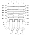
ここで、蓄積部の垂直CCDシフトレジスタの出力端と水平転送部との間に情報電荷を振り分ける機構を備えたCCDイメージセンサの構造が知られている。当該振り分け機構を設けることにより、蓄積部の垂直CCDシフトレジスタから出力される1行分の情報電荷を、奇数列の情報電荷群と偶数列の情報電荷群とに分けて、水平転送部へ転送することができる。この構成では、水平転送部を構成する水平CCDシフトレジスタは、奇数列の情報電荷群及び偶数列の情報電荷群について別々に水平転送動作を行い、1行分の情報電荷の水平転送動作を完了する。図6は、この振り分け機構を有する従来のフレーム転送方式のCCDイメージセンサの駆動方法を説明するタイミング図であり、蓄積部及び水平転送部を駆動する各クロック信号の波形を示している。また、図7は、図6に示す各時刻における転送電極下のチャネル電位を示す模式図である。図7において、下向きがチャネル電位の正の向きであり、電荷転送チャネルに沿ったポテンシャルの深さの変化を実線で表しており、実線が下に窪んだ部分が電子からなる情報電荷を蓄積可能な電位井戸となる。ここで示す蓄積部の垂直CCDシフトレジスタは、3相クロック信号φ1〜φ3を用いた3相駆動であり、各ビットに3本の転送電極ST1〜ST3が配置される。転送電極ST1〜ST3は電荷転送方向に沿って順番に並び、STiにクロック信号φi(i=1〜3)が印加される。φiが所定の高電圧VHであるとき、転送電極STiの下には電位井戸が形成され、情報電荷の蓄積が可能となり、一方、所定の低電圧VLであるとき、転送電極STiの下には電位井戸間を仕切る電位障壁が形成される。クロック信号φHは、水平CCDシフトレジスタを駆動するクロック信号である。φHにもφiと同様、所定の高電圧状態及び低電圧状態があり、それらが周期的に切り替わることで、情報電荷の水平転送が実現される。 Here, a structure of a CCD image sensor having a mechanism for distributing information charges between an output terminal of a vertical CCD shift register of a storage unit and a horizontal transfer unit is known. By providing the distribution mechanism, one row of information charges output from the vertical CCD shift register of the storage unit is divided into odd-numbered information charge groups and even-numbered information charge groups and transferred to the horizontal transfer unit. can do. In this configuration, the horizontal CCD shift register constituting the horizontal transfer unit separately performs the horizontal transfer operation for the odd-numbered information charge group and the even-numbered information charge group and completes the horizontal transfer operation of the information charge for one row. To do. FIG. 6 is a timing chart for explaining a driving method of a conventional frame transfer type CCD image sensor having this distribution mechanism, and shows waveforms of clock signals for driving the storage unit and the horizontal transfer unit. FIG. 7 is a schematic diagram showing the channel potential under the transfer electrode at each time shown in FIG. In FIG. 7, the downward direction is the positive direction of the channel potential, the change in the depth of the potential along the charge transfer channel is represented by a solid line, and the portion where the solid line is depressed downward can store information charges consisting of electrons. Potential well. The vertical CCD shift register of the storage unit shown here is a three-phase drive using three-phase clock signals φ 1 to φ 3 , and three transfer electrodes ST 1 to ST 3 are arranged for each bit. The transfer electrodes ST1 to ST3 are arranged in order along the charge transfer direction, and a clock signal φ i (i = 1 to 3) is applied to STi. When φ i is a predetermined high voltage V H , a potential well is formed under the transfer electrode STi, and information charges can be accumulated. On the other hand, when φ i is a predetermined low voltage V L , A potential barrier for partitioning the potential wells is formed below. Clock signal phi H is a clock signal for driving the horizontal CCD shift register. Similarly to φ i, φ H has a predetermined high voltage state and low voltage state, and these are switched periodically to realize horizontal transfer of information charges.
期間P1ではライン転送動作が行われ、撮像部の垂直CCDシフトレジスタの各ビットの転送電極ST2及びST3の下に形成された電位井戸が次のビットの転送電極ST2及びST3の下に移動される。期間P1に対応する各時刻t1〜t7での電位井戸の様子を図7に表している。この電位井戸の移動と共に、情報電荷も垂直CCDシフトレジスタ内を1ビット移動する。 Period P 1 in the line transfer operation is performed, the potential wells formed under the transfer electrodes ST2 and ST3 of each bit of the vertical CCD shift register of the imaging section is moved under the next bit transfer electrodes ST2 and ST3 The FIG. 7 shows the state of the potential well at each time t 1 to t 7 corresponding to the period P 1 . Along with the movement of the potential well, the information charge moves 1 bit in the vertical CCD shift register.
ライン転送動作に引き続き、期間P2にて水平転送動作が行われる。水平転送動作では、まず、奇数列情報電荷群を水平CCDシフトレジスタに読み出す動作が行われ、その後、当該奇数列情報電荷群は期間POにて連続発生されるφHのクロック列により出力部に転送される。さらに水平転送動作の期間P2では、偶数列情報電荷群を水平CCDシフトレジスタに読み出す動作が行われ、当該偶数列情報電荷群は期間PEにて連続発生されるφHのクロック列により出力部に転送される。このようにして、1行分の水平転送動作が完了すると、期間P3にて次のライン転送が行われる。 Following the line transfer operation, the horizontal transfer operation is performed in the period P 2. In the horizontal transfer operation, first, the operation of reading the odd column information charge packets to the horizontal CCD shift register is carried out, then the odd column information charge packets output unit by a clock sequence of phi H that is continuously generated in the period P O Forwarded to Furthermore in the period P 2 of the horizontal transfer operation, the operation of reading the even column information charge packets to the horizontal CCD shift register is carried out, the even-numbered column information charge packets output by the clock row of phi H that is continuously generated in the period P E Forwarded to the department. In this way, when the horizontal transfer operation for one line is completed, the next line is transferred in the period P 3.
この水平転送動作を行う期間P2の全体又は少なくとも期間PO及びPEにおいては、蓄積部の垂直CCDシフトレジスタの各ビットに保持される情報電荷は、ライン転送での移動先である2つの転送電極ST2及びST3の下の電位井戸に存在する。すなわち、従来は、蓄積部の垂直CCDシフトレジスタの各ビットの情報電荷は、先行するライン転送動作期間P1の終了から次のライン転送動作期間P3の開始まで、基本的に、時刻t7での移動先の転送電極ST2及びST3の下に保持される。
埋込チャネルのCCDシフトレジスタでは、情報電荷を基板表面近くまで蓄積すると、界面準位により情報電荷がトラップされ、転送効率が低下し得る。ここで、界面準位の密度は基板面内で一様ではないため、一般に、蓄積部の垂直CCDシフトレジスタ相互間に転送効率のばらつきが生じる。その転送効率の差異は、撮影された画像にて縦すじとして現れ、画質劣化の要因となる。 In the CCD shift register of the buried channel, when the information charge is accumulated close to the substrate surface, the information charge is trapped by the interface state, and the transfer efficiency can be lowered. Here, since the density of interface states is not uniform within the substrate surface, in general, the transfer efficiency varies between the vertical CCD shift registers of the storage unit. The difference in transfer efficiency appears as a vertical streak in the photographed image, which causes image quality degradation.
トラップされる電荷量は、情報電荷を基板表面近くまで蓄積した状態の持続時間に応じて増加し得る。上述の蓄積部の動作においては、水平転送期間での情報電荷の保持動作が、ライン転送動作の各過程に比べて長時間であるため、この保持動作でのトラップの発生を抑制することが縦すじの軽減に有効である。 The amount of charge trapped can increase with the duration of the state in which the information charge is accumulated close to the substrate surface. In the above-described operation of the storage unit, the holding operation of the information charge in the horizontal transfer period is longer than each process of the line transfer operation. Effective for reducing streaks.
ちなみに、デジタルカメラ等の撮像装置では、静止画は固体撮像素子の画素数に応じた高精細の画質で撮影し、動画は画素数を間引いてフレームレートを確保することが行われる。行を間引かずに読み出す静止画撮影はライン転送動作及び保持動作の繰り返し回数が動画撮影より多くなり得、当該動作の繰り返し毎の転送効率の累積により、縦すじが動画撮影時より顕著となり得る。その一方で、静止画撮影は動画撮影より高画質が要求されるため、縦すじを好適に抑制することが必要とされる。 Incidentally, in an imaging device such as a digital camera, a still image is taken with a high-definition image quality corresponding to the number of pixels of a solid-state imaging device, and a moving image is obtained by thinning out the number of pixels to ensure a frame rate. Still image shooting that reads without thinning out lines can have more repetitions of line transfer and holding operations than movie shooting, and vertical streaks can be more noticeable than movie shooting due to the accumulation of transfer efficiency for each repetition of the operation. . On the other hand, since still image shooting requires higher image quality than moving image shooting, it is necessary to suitably suppress vertical stripes.
さて、所定深さの電位井戸に情報電荷を蓄積する場合、情報電荷は、電位井戸の面積が小さいほど基板表面に近づきやすく、逆に面積が大きいほど基板表面と距離を保つことが容易である。以上のような点から、静止画における縦すじを好適に抑制する上で上述の従来の駆動方法、すなわち、蓄積部の3相駆動の垂直CCDシフトレジスタにおいて、水平転送期間にて情報電荷を保持する電位井戸を、1相分の転送電極下だけでなく、2相分の転送電極下に形成する駆動方法は有効である。 When storing information charges in a potential well of a predetermined depth, the information charges are more likely to approach the substrate surface as the area of the potential well is smaller, and conversely, the distance from the substrate surface is easier as the area is larger. . In view of the above points, the information charge is retained in the horizontal transfer period in the conventional driving method described above, that is, in the vertical CCD shift register of the three-phase drive of the storage unit, in order to suitably suppress the vertical stripe in the still image. A driving method in which the potential well to be formed is formed not only under the transfer electrode for one phase but also under the transfer electrode for two phases is effective.
このように従来の駆動方法は、水平転送期間での情報電荷の保持動作にて2つの転送電極下に情報電荷を保持してトラップを抑制する。しかし、ライン転送動作の途中では、図7の時刻t2,t4,t6のように1つの相の転送電極下だけに情報電荷が蓄積される期間が短時間ではあるが存在し、当該期間にて情報電荷のトラップが起こり得る。そして、或るビットの転送電極下にトラップされた電荷は、ライン転送によって次の情報電荷が当該転送電極下に移動してきた際に放出され混入し、画質劣化の原因となるという問題があった。例えば、撮像部において垂直方向に並ぶ画素に互いに異なる色のカラーフィルタを配置した構成では、上記トラップ電荷の混入は混色という現象を生じ、これは表示画面にて色バランスの崩れとして観察される。 Thus, the conventional driving method suppresses traps by holding information charges under the two transfer electrodes in the holding operation of information charges in the horizontal transfer period. However, in the middle of the line transfer operation, there is a short period in which information charges are accumulated only under one phase of the transfer electrode as shown at times t 2 , t 4 , and t 6 in FIG. Information charge traps can occur over time. The charge trapped under the transfer electrode of a certain bit has a problem that it is released and mixed when the next information charge moves under the transfer electrode by line transfer, causing deterioration in image quality. . For example, in a configuration in which color filters of different colors are arranged in pixels arranged in the vertical direction in the imaging unit, the mixing of the trapped charges causes a phenomenon of color mixing, which is observed as a color balance disruption on the display screen.
本発明は上記問題点を解決するためになされたものであり、縦すじを抑制しつつ、垂直方向に隣接する画素間の情報電荷へのトラップ電荷の混入を抑制して、混色等の不具合を回避し、画質の向上が図られる固体撮像素子の駆動方法を提供することを目的とする。 The present invention has been made in order to solve the above-mentioned problems, and while suppressing vertical streaks, it suppresses the mixing of trapped charges into information charges between pixels adjacent in the vertical direction, thereby preventing problems such as color mixing. An object of the present invention is to provide a driving method of a solid-state imaging device that can be avoided and improved in image quality.
本発明に係る固体撮像素子の駆動方法は、行列配置された受光画素にて発生した情報電荷を列方向に垂直転送するn相駆動(nは3以上の自然数である)可能な複数の垂直CCDシフトレジスタと、前記複数の垂直CCDシフトレジスタから出力される前記情報電荷を行方向に水平転送する水平CCDシフトレジスタとを有する固体撮像素子を駆動する駆動方法であって、前記各垂直CCDシフトレジスタにて前記情報電荷を1ビットずつ移動させることにより、前記情報電荷を1行ずつ垂直転送するライン転送動作と、前記ライン転送動作により前記複数の垂直CCDシフトレジスタから出力される1行分の前記情報電荷を、前記水平CCDシフトレジスタにより水平転送する水平転送動作と、前記水平転送動作を行う期間において、前記垂直CCDシフトレジスタ上の前記情報電荷を現在位置しているビットに保持する情報電荷保持動作と、を有し、前記情報電荷保持動作が、直近に行われた前記ライン転送動作の期間に続いて始まり前記水平転送動作の途中までの第1期間において、前記垂直CCDシフトレジスタのビット毎に配置された一組の転送電極のうちm1本の転送電極下に前記情報電荷を蓄積する第1蓄積動作と、前記第1期間後に始まり次の前記ライン転送動作の期間の開始までの第2期間にて、前記一組の転送電極のうち、前記m1本より多いm2本の下に前記情報電荷を蓄積する第2蓄積動作と、を有する方法である。 The solid-state imaging device driving method according to the present invention includes a plurality of vertical CCDs capable of n-phase driving (n is a natural number of 3 or more) for vertically transferring information charges generated in light receiving pixels arranged in a matrix in the column direction. A driving method for driving a solid-state imaging device, comprising: a shift register; and a horizontal CCD shift register that horizontally transfers the information charges output from the plurality of vertical CCD shift registers in a row direction. The information charges are moved bit by bit by a line transfer operation for vertically transferring the information charges line by line, and the line transfer operation for one line output from the plurality of vertical CCD shift registers. A horizontal transfer operation in which information charges are horizontally transferred by the horizontal CCD shift register, and a period in which the horizontal transfer operation is performed. An information charge holding operation for holding the information charge on the direct CCD shift register in the bit currently located, and the information charge holding operation follows the period of the most recently performed line transfer operation. First accumulation in which the information charges are accumulated under m 1 transfer electrodes of a set of transfer electrodes arranged for each bit of the vertical CCD shift register in a first period beginning to the middle of the horizontal transfer operation In the second period starting from the first period until the start of the next line transfer operation period, the information is under m 2 more than m 1 in the set of transfer electrodes. And a second accumulation operation for accumulating electric charge.
他の本発明に係る固体撮像素子の駆動方法は、前記ライン転送動作により前記複数の垂直CCDシフトレジスタから出力される1行分の前記情報電荷を第1乃至第k(kは2以上の自然数である)の情報電荷群に分割して当該情報電荷群毎に順次、前記水平CCDシフトレジスタへ転送する振り分け転送機構を有する固体撮像素子を駆動する際の上記駆動方法であって、前記水平転送動作が、前記第1乃至第kの情報電荷群それぞれを水平転送する第1乃至第kの群別水平転送動作を順次行い、前記情報電荷保持動作が、前記群別水平転送動作相互のk−1個の間隔のいずれかに同期して、前記第1蓄積動作から前記第2蓄積動作への切り換えを行う。 In another solid-state imaging device driving method according to the present invention, the information charges for one row output from the plurality of vertical CCD shift registers by the line transfer operation are converted into first to kth (k is a natural number of 2 or more). The above-mentioned driving method for driving a solid-state imaging device having a distribution transfer mechanism that divides the information charge group and transfers the information charge group sequentially to the horizontal CCD shift register. The operation sequentially performs first to k-th group horizontal transfer operations for horizontally transferring each of the first to k-th information charge groups, and the information charge holding operation is performed between the group horizontal transfer operations. Switching from the first accumulation operation to the second accumulation operation is performed in synchronization with any one interval.
上記駆動方法において、前記第1期間の長さは、前記垂直CCDシフトレジスタのチャネルを構成する半導体基板の界面準位がトラップした電荷を放出する過程の時定数に応じて設定することが好適である。 In the above driving method, it is preferable that the length of the first period is set in accordance with a time constant of a process of discharging charges trapped by an interface state of a semiconductor substrate constituting a channel of the vertical CCD shift register. is there.
また、前記ライン転送動作により前記複数の垂直CCDシフトレジスタから出力される1行分の前記情報電荷を、奇数列に対応する情報電荷群と偶数列に対応する情報電荷群とに分割して当該情報電荷群を順次、前記水平CCDシフトレジスタへ転送する振り分け転送機構を有する固体撮像素子を駆動する際の上記駆動方法は、前記水平転送動作が、前記奇数列の情報電荷群を水平転送する奇数列水平転送動作と前記偶数列の情報電荷群を水平転送する偶数列水平転送動作とを順次行い、前記情報電荷保持動作が、前記奇数列水平転送動作と前記偶数列水平転送動作との間隔に同期して前記第1蓄積動作から前記第2蓄積動作への切り換えを行うように構成することができる。 The information charges for one row output from the plurality of vertical CCD shift registers by the line transfer operation are divided into information charge groups corresponding to odd columns and information charge groups corresponding to even columns. The driving method for driving a solid-state imaging device having a distribution transfer mechanism that sequentially transfers information charge groups to the horizontal CCD shift register is the odd number in which the horizontal transfer operation horizontally transfers the information charge groups in the odd columns. A column horizontal transfer operation and an even column horizontal transfer operation for horizontally transferring the information charge group of the even column are sequentially performed, and the information charge holding operation is performed at an interval between the odd column horizontal transfer operation and the even column horizontal transfer operation. It can be configured to switch from the first accumulation operation to the second accumulation operation in synchronization.
上記駆動方法は、前記垂直CCDシフトレジスタが3相駆動可能である固体撮像素子に適用する際に、前記第1蓄積動作が、前記3相駆動のうちの1つの相に対応する前記転送電極の下に前記情報電荷を蓄積し、前記第2蓄積動作が、前記3相駆動のうちの2つの相に対応する前記転送電極の下に前記情報電荷を蓄積するように構成することができる。 When the driving method is applied to a solid-state imaging device in which the vertical CCD shift register is capable of three-phase driving, the first accumulation operation is performed on the transfer electrode corresponding to one phase of the three-phase driving. The information charge can be stored below, and the second storage operation can be configured to store the information charge under the transfer electrode corresponding to two phases of the three-phase driving.
別の本発明に係る固体撮像素子の駆動方法は、前記第1蓄積動作にて、前記各ビットに蓄積される前記情報電荷に対する電位障壁を形成する前記転送電極に、前記ライン転送動作における転送クロックのオフ電圧より低い第1蓄積動作時オフ電圧を印加する方法である。前記第1蓄積動作時オフ電圧は、前記転送電極下の半導体表面に反転層を形成するピンニング電圧に応じた値とすることができる。 Another solid-state imaging device driving method according to the present invention is the transfer clock in the line transfer operation on the transfer electrode that forms a potential barrier against the information charge stored in each bit in the first storage operation. This is a method of applying an off voltage during the first accumulation operation that is lower than the off voltage. The off voltage during the first accumulation operation may be a value corresponding to a pinning voltage for forming an inversion layer on the semiconductor surface under the transfer electrode.
本発明によれば、ライン転送動作後の垂直CCDシフトレジスタでの情報電荷の保持動作を、水平転送期間の途中までの期間(第1期間)は狭い電位井戸に情報電荷を蓄積し、その後の期間(第2期間)は広い電位井戸に情報電荷を蓄積する動作とする。トラップ電荷の放出はトラップされてからの時間と共に低減することが期待できる。そこで、ライン転送動作の途中でのトラップ電荷が放出され易い第1期間にて、電位井戸を狭くすることで、トラップ電荷のうち電位井戸に対応する転送電極下にて放出される分が少なくなり、当該対応転送電極下から電位井戸に直接、流れ込むトラップ電荷量が抑制され、混色の低減が図られる。一方、第1期間より後の第2期間にて電位井戸を広げて、情報電荷を基板表面から遠ざけることで、保持動作での電位井戸からトラップされる情報電荷量を抑制すると共に、第1期間にて既に当該電位井戸からトラップされた情報電荷を元の電位井戸に放出させることができる。これにより、保持動作でのトラップの発生が抑制され、縦すじの軽減が図られる。 According to the present invention, in the information charge holding operation in the vertical CCD shift register after the line transfer operation, the information charge is accumulated in the narrow potential well during the period until the middle of the horizontal transfer period (first period). In the period (second period), information charges are stored in a wide potential well. It can be expected that the emission of trapped charges decreases with the time after trapping. Therefore, by narrowing the potential well in the first period during which the trap charge is likely to be released during the line transfer operation, the portion of the trap charge released under the transfer electrode corresponding to the potential well is reduced. Therefore, the amount of trap charges flowing directly from below the corresponding transfer electrode into the potential well is suppressed, and color mixing is reduced. On the other hand, by expanding the potential well in the second period after the first period and keeping the information charges away from the substrate surface, the amount of information charges trapped from the potential well in the holding operation is suppressed, and the first period The information charge already trapped from the potential well can be released to the original potential well. Thereby, generation | occurrence | production of the trap by holding | maintenance operation | movement is suppressed and a vertical streak is reduced.
また、第1期間において、情報電荷を蓄積する電位井戸に隣接する電位障壁を形成する転送電極に、ライン転送動作における転送クロックのオフ電圧より低い第1蓄積動作時オフ電圧を印加することで、当該転送電極下にて情報電荷とは反対極性であるホールの発生を促し、ライン転送動作で生じたトラップ電荷と当該ホールとの再結合を促進させる。これにより、当該転送電極下にてトラップ電荷が放出され隣接する電位井戸に流れ込むことが抑制され、混色の低減が図られる。 Further, in the first period, by applying an off voltage during the first accumulation operation lower than the off voltage of the transfer clock in the line transfer operation to the transfer electrode forming the potential barrier adjacent to the potential well for accumulating information charges, The generation of a hole having a polarity opposite to that of the information charge under the transfer electrode is promoted, and the recombination between the trap charge generated in the line transfer operation and the hole is promoted. Thereby, trapped charges are released under the transfer electrode and are prevented from flowing into the adjacent potential well, thereby reducing color mixing.
以下、本発明の実施の形態(以下実施形態という)について、図面に基づいて説明する。 Hereinafter, embodiments of the present invention (hereinafter referred to as embodiments) will be described with reference to the drawings.
図1は、実施形態である撮像装置の概略の構成を示すブロック図である。この撮像装置は、イメージセンサ10及び駆動回路12を含み、イメージセンサ10から画像信号を出力する。
FIG. 1 is a block diagram illustrating a schematic configuration of an imaging apparatus according to the embodiment. The imaging apparatus includes an
イメージセンサ10は、フレーム転送方式のCCDイメージセンサであり、半導体基板表面に形成された撮像部10i、蓄積部10s、水平転送部10h、出力部10d及び振り分け部10tを備える。
The
撮像部10i及び蓄積部10sは互いに列方向に互いの電荷転送チャネルが連続した垂直CCDシフトレジスタからなり、撮像部10i及び蓄積部10sにはそれら垂直CCDシフトレジスタが行方向(画像上の水平方向)に複数配列される。これら垂直CCDシフトレジスタは転送電極として、基板上に行方向に渡され、かつ列方向に複数本並列に配列されたゲート電極を備える。撮像部10iの垂直CCDシフトレジスタの各ビットは受光画素を構成し、入射光に応じて信号電荷を発生し蓄積する。蓄積部10sは遮光膜で覆われ、光の入射による電荷発生を防止されるので、フレーム転送された撮像部10iからの信号電荷を基本的にそのまま保持することができる。
The
振り分け部10tは蓄積部10sの出力端と水平転送部10hとの間に位置し、蓄積部10sの各垂直CCDシフトレジスタから延長される電荷転送チャネルと、蓄積部10sとは独立に駆動可能な転送電極である複数本のトランスファゲート電極(TG電極)とから構成される。振り分け部10tは情報電荷の振り分け機構であり、蓄積部10sの垂直CCDシフトレジスタ群から出力される1行分の情報電荷を、奇数列の情報電荷群と偶数列の情報電荷群とに分けて、水平転送部10hへ転送する。
The
水平転送部10hはCCDシフトレジスタからなり、その各ビットは振り分け部10tの各電荷転送チャネルの出力端に接続される。
The
出力部10dは、電気的に独立した容量及びその電位変化を取り出すアンプからなり、水平転送部10hから出力される信号電荷を1ビット単位で容量に受けて電圧値に変換し、時系列の画像信号Y0(t)として出力する。
The
駆動回路12は、各種クロック信号や電圧信号を生成してイメージセンサ10を駆動する。撮像部10iの垂直CCDシフトレジスタの転送電極には複数相の転送クロックφI、蓄積部10sの垂直CCDシフトレジスタの転送電極には複数相の転送クロックφSが駆動回路12から供給され、これら転送クロックにより、撮像部10i及び蓄積部10sにおける情報電荷の蓄積、転送が制御される。また、駆動回路12は、TG電極を駆動するクロックφTG、水平転送部10hを駆動するクロックφH、出力部10dのリセットゲートを駆動するクロックφR、n型半導体基板に印加される基板電圧Vsubなどを生成する。
The
本イメージセンサ10の垂直CCDシフトレジスタの各ビットには、それぞれ3本の転送電極が配置される。撮像部10iにはカラーフィルタアレイが配置され、撮像部10iの垂直CCDシフトレジスタの各ビットは、それぞれ特定の一色のカラーフィルタを配置された受光画素を構成する。例えば、撮像部10iは、ベイヤー配列のカラーフィルタアレイを配置され、色感度特性の異なる2種類の受光画素が列方向に交互に配置される。
Three transfer electrodes are arranged in each bit of the vertical CCD shift register of the
この撮像部10iにおいて、動画撮影やプレビューでの画素圧縮した撮影を可能とするために、例えば、各垂直CCDシフトレジスタの連続する3ビット毎の9本の転送電極が互いに独立に駆動可能に構成される。静止画撮影では、各ビットの3本の転送電極それぞれを別相とした3相駆動である標準的な駆動が行われる。一方、動画撮影及びプレビューでは、撮像部10iの列方向に連続する3画素ずつで信号電荷の加算合成処理を行ってからフレーム転送を行う画素圧縮駆動が行われる。例えば、3画素のうち中央の画素を間引いて、その両側の互いに同じ色の画素の信号電荷を加算する画素加算処理が行われる。この画素加算処理は、具体的には、まず3画素のうち中央の画素の3本の転送電極にオフ電圧を印加することで、当該画素に蓄積された信号電荷を比較的高い正の基板電圧Vsubを印加した基板へ移動させて排出し、その後、当該画素の両側の2画素に蓄積される信号電荷を合成する。画素圧縮動作では、このように3画素を単位とした加算合成処理を行った後、撮像部10i,蓄積部10sの各ビットの3本の転送電極を同相とした3相駆動を行う。この画素圧縮駆動により、静止画撮影に比べて実質的な垂直方向の画素数を1/3に圧縮することができ、例えば、標準的な駆動時と同じクロック周波数で3倍高速のフレーム転送が実現され、またライン転送の回数が1/3に低減される。
In this
縦すじ及び混色を抑制し画質向上を図る本発明の駆動方法は、静止画撮影、動画撮影及びプレビューを問わず適用することができるが、静止画撮影では、ライン転送回数が多いために画質がより劣化し易い反面、一層の高画質を要求される点で特に本発明が有効である。そこで、以下、静止画撮影時における本発明の駆動方法を具体的に説明する。 The drive method of the present invention that improves image quality by suppressing vertical stripes and color mixing can be applied regardless of still image shooting, movie shooting, and preview. However, in still image shooting, image quality is low because of the large number of line transfers. While being easily deteriorated, the present invention is particularly effective in that higher image quality is required. Therefore, the driving method of the present invention at the time of still image shooting will be specifically described below.
撮像部10iの受光画素は露光期間中の入射光に応じて信号電荷を発生し蓄積する。設定された露光期間が経過すると、駆動回路12は、3相クロックφI,φSにより撮像部10i及び蓄積部10sそれぞれの垂直CCDシフトレジスタを駆動し、撮像部10iから蓄積部10sへ情報電荷をフレーム転送する。そして、駆動回路12は、蓄積部10sに転送された1画面分の信号電荷を、ライン転送動作及び水平転送動作を繰り返すことにより1行ずつ読み出して、画像信号に変換する。この駆動回路12による駆動のうち、従来の駆動方法との主たる相違点は、フレーム転送後における蓄積部10sにおけるライン転送動作にあり、以下、この点を詳述する。
The light receiving pixels of the
図2は、イメージセンサ10の蓄積部10s、振り分け部10t及び水平転送部10hの概略の構造示す平面図である。蓄積部10sの各垂直CCDシフトレジスタの列方向に延伸するチャネル領域20が、相互間をチャネルストップ領域22により分離される。蓄積部10sの各ビットには3本の転送電極ST1〜ST3が配置される。転送電極ST1〜ST3は電荷転送方向に沿って順番に並び、駆動回路12からSTiにクロック信号φSi(i=1〜3)が印加される。
FIG. 2 is a plan view illustrating a schematic structure of the
振り分け部10tには、蓄積部10sの垂直CCDシフトレジスタの最終ビットの転送電極ST3に隣接配置された転送電極ST1と、4本のTG電極TG1〜TG4とが配置される。TG1及びTG2は、列方向の互いの位置が列毎に交互に逆転する蛇行した形状を有する。振り分け部10tに配置された前記転送電極ST1とTG1及びTG2の対との間にはTG4が配置され、水平転送部10hとTG1及びTG2の対との間にはTG3が配置される。これらTG3及びTG4はそれぞれ行方向に延びる直線形状に構成される。奇数列のチャネル領域20上では、TG1はTG4とTG2との間の領域のチャネル電位を制御し、TG2はTG1とTG3との間の領域のチャネル電位を制御する。一方、偶数列のチャネル領域20上では、TG2はTG4とTG1との間の領域のチャネル電位を制御し、TG1はTG2とTG3との間の領域のチャネル電位を制御する。TG電極TGiは駆動回路12からクロック信号φTGi(i=1〜4)を印加される。
In the
水平転送部10hを構成する水平CCDシフトレジスタは、チャネル領域24及び水平転送電極26-1,26-2から構成される。チャネル領域24は振り分け部10t側においてチャネル領域20及びチャネルストップ領域22に接し、反対側の境界はチャネルストップ領域28に接する。水平転送電極26-1は、TG3とチャネルストップ領域28との間に設けられ、チャネル領域24のうち各チャネル領域20につながる部分に配置される。水平転送電極26-2は、2つの水平転送電極26-1の間のチャネル領域24上を覆うように配置される。水平CCDシフトレジスタは2相駆動であり、水平転送電極26-1に対応するチャネル領域24が情報電荷を蓄積するストレージ領域を構成し、水平転送電極26-2に対応するチャネル領域24は、不純物を注入してチャネル電位をストレージ領域より浅くしたバリア領域を構成する。互いに隣接する水平転送電極26-1,26-2からなる各電極対は互いに電気的に接続され、奇数列のチャネル領域20に対応する位置の電極対HS1には水平転送クロックφH1が印加され、偶数列のチャネル領域20に対応する位置の電極対HS2には水平転送クロックφH2が印加される。
The horizontal CCD shift register constituting the
図3は、蓄積部10sにフレーム転送された情報電荷を水平転送部10hへ読み出す動作のタイミング図であり、蓄積部10s、振り分け部10t及び水平転送部10hを駆動する各クロック信号の波形を示している。また、図4、図5は、図3に示す各時刻での各転送電極下のチャネル電位を示す模式図である。図4は奇数列の電荷転送チャネルについて、また図5は偶数列の電荷転送チャネルについての図である。図4、図5それぞれの最上部には、電荷転送チャネルに沿った転送電極の配列を、図において電荷転送方向を右向きに取って示し、その下に、各転送電極下でのチャネル電位を、時系列に従って縦方向に並べて示している。チャネル電位は図7と同様、下向きを正の向きとして表しており、電荷転送チャネルに沿ったチャネル電位の深さの変化を実線で表しており、実線が下に窪んだ部分が電子からなる情報電荷を蓄積可能な電位井戸となる。また、電位井戸に蓄積される情報電荷を斜線又は網掛けパターンで示している。
FIG. 3 is a timing chart of an operation of reading the information charges frame-transferred to the
駆動回路12は、クロック信号φSi(i=1〜3)に関して、オン電圧VH及び2種類のオフ電圧VL1,VL2を生成し、タイミングに応じてVH,VL1,VL2のいずれかをφSiとして出力する。ここで、オン電圧VHは所定の正電圧であり、当該電圧を印加された転送電極の下のチャネル電位は深くなり、当該転送電極下には、電子からなる情報電荷を蓄積可能な電位井戸が形成される。2種類のオフ電圧VL1,VL2は、VH>VL1>VL2なる大小関係を有する。フレーム転送動作やライン転送動作におけるオフ電圧はVL1に設定される。一方、所定の負電圧に設定されるVL2は、後述するように水平転送動作中における蓄積部10sでの情報電荷の保持動作において利用される。例えば、VL2はピンニング電圧のように、これを印加した転送電極下の基板表面に、ホールが蓄積した反転層が形成される電圧に設定される。
Drive
駆動回路12は、クロック信号φTGi(i=1〜4)に関して、オン電圧VH及びオフ電圧VL1を生成し、タイミングに応じてVH,VL1のいずれかをφTGiとして出力する。また、駆動回路12は、クロック信号φHi(i=1,2)に関して、オン電圧VHH及びオフ電圧VHL(VHH>VHL)を生成し、タイミングに応じてVHH,VHLのいずれかをφHiとして出力する。なお、VHを印加したときのSTi及びTGi下のチャネル領域20でのチャネル電位と、VHHを印加したときのHSiのストレージ領域でのチャネル電位とは必ずしも同じでなくてもよく、またVL1を印加したときのSTi及びTGi下のチャネル電位と、VHLを印加したときのHSiのストレージ領域でのチャネル電位とは必ずしも同じでなくてもよいが、便宜上、図4及び図5では、垂直転送に係るチャネル領域20及び水平転送部10hのストレージ領域それぞれのオン電圧印加時のチャネル電位が互いに同じであり、またオフ電圧印加時のチャネル電位が互いに同じとして表している。
The
時刻t1において、イメージセンサ10の各部は、フレーム転送動作直後の状態又は先行する水平転送動作が完了した状態にある。この状態では、蓄積部10sに保持される情報電荷は転送電極ST2及びST3の下に形成される電位井戸に蓄積される。この状態に引き続いて、ライン転送動作が行われる。図3〜図5における時刻t1から時刻t6までの間に、ライン転送動作が行われ、蓄積部10sの垂直CCDシフトレジスタの各ビットに保持された情報電荷が1ビットずつ水平転送部10hへ向けて移動する。この動作を詳細に説明する。時刻t1にて或るビットのST2及びST3の下に蓄積されていた情報電荷は、φS2がオン電圧VHからオフ電圧VL1へ遷移し(時刻t2)、さらにφS1がVL1からVHへ遷移することにより(時刻t3)、ST3の下だけに蓄積される状態(時刻t2)を経由して、ST3及び次のビットのST1の下に形成される電位井戸へ移動する(時刻t3)。同様に、φS3がVL1へ遷移し(時刻t4)、さらにφS2がVL1からVHへ遷移することにより(時刻t5)、情報電荷は、時刻t3におけるST3及びST1の下に蓄積された状態から、一旦、ST1の下だけに蓄積される状態(時刻t4)を経由して、次のビットのST1及びST2の下に形成される電位井戸へ移動する(時刻t5)。
At time t 1, each part of the
本駆動方法では、情報電荷をST1及びST2の下に蓄積した情報電荷を、次にST2だけの下に集め(時刻t6)、この状態でライン転送動作を終え、水平転送動作を開始する。つまり、ライン転送動作は、或るビットのST2及びST3の下に保持されていた情報電荷を、次のビットのST2の下だけに形成される電位井戸へ移動する。これにより、水平転送動作の開始に際して、蓄積部10sは従来より狭い電位井戸に情報電荷を保持する。これに対して、従来の駆動方法は、情報電荷をST1及びST2の下に蓄積した情報電荷を、ST2だけの下に蓄積される状態を経由して、ST2及びST3の下に形成される電位井戸へ移動した段階でライン転送動作を終える。つまり、従来のライン転送動作は、或るビットのST2及びST3の下に保持されていた情報電荷を、次のビットのST2及びST3の下に形成される電位井戸へ移動し、この電位井戸に情報電荷を保持した状態で水平転送動作を開始する。ここに、本駆動方法と従来の駆動方法との一つの相違点がある。
In this driving method, the information charges accumulated under ST1 and ST2 are then collected only under ST2 (time t 6 ), the line transfer operation is finished in this state, and the horizontal transfer operation is started. In other words, in the line transfer operation, the information charges held under ST2 and ST3 of a certain bit are moved to a potential well formed only under ST2 of the next bit. Thus, at the start of the horizontal transfer operation, the
なお、蓄積部10sの垂直CCDシフトレジスタの出力端のビットに保持されていた情報電荷40,42は、上記ライン転送動作により、振り分け部10tに移動する。
The information charges 40 and 42 held in the output end bit of the vertical CCD shift register of the
ここでいう水平転送動作は、振り分け部10tが奇数列の情報電荷と偶数列の情報電荷とを振り分けて水平CCDシフトレジスタへ出力する動作(振り分け動作)と、振り分け出力された情報電荷を水平CCDシフトレジスタにより水平転送する動作(狭義の水平転送動作)とからなる。具体的には、ライン転送動作後、駆動回路12は、水平転送動作として、奇数列の情報電荷40を振り分け部10tから水平CCDシフトレジスタへ転送する奇数列振り分け転送動作(時刻t7〜t12)、水平CCDシフトレジスタを駆動して奇数列情報電荷40を水平転送する奇数列水平転送動作(期間PO)、偶数列の情報電荷42を振り分け部10tから水平CCDシフトレジスタへ転送する偶数列振り分け転送動作(時刻t13〜t17)、及び水平CCDシフトレジスタを駆動して偶数列情報電荷42を水平転送する偶数列水平転送動作(期間PE)を順次実行する。
In this horizontal transfer operation, the distributing
水平転送動作の期間、蓄積部10sの各ビットに保持される情報電荷は、上述のように、ライン転送動作の終了時には、単一の転送電極ST2の下だけに蓄積されるが、所定時間経過後、駆動回路12はφS3をVHへ遷移させ、次のライン転送動作の開始まで、ST2及びST3の下に形成される電位井戸に情報電荷を蓄積する。すなわち、駆動回路12は、ライン転送動作の終了から水平転送動作の途中までの第1の期間において、蓄積部10sの垂直CCDシフトレジスタのビット毎に配置された一組の転送電極のうちの1本の転送電極下に情報電荷を蓄積する第1の蓄積動作と、前記第1の期間後に始まり次のライン転送動作の開始までの第2の期間にて、前記一組の転送電極のうち、前記第1蓄積動作時より多い2本の下に情報電荷を蓄積する第2の蓄積動作とを切り替える。
During the horizontal transfer operation, the information charges held in each bit of the
既に述べたように、ライン転送動作の途中の電位井戸が狭くなるタイミングでは、情報電荷が基板表面近くまで蓄積され、界面準位にトラップされ易くなる。そして、界面準位は、ライン転送動作において先行して通過するビットの情報電荷をトラップし、後続ビットの電位井戸へ放出することにより、混色の問題が発生し得る。第1蓄積動作は、当該問題の軽減を図るものであり、情報電荷を蓄積する電位井戸を狭く形成することで、当該電位井戸に対応する転送電極下にて放出されるトラップ電荷の減少を図り、混色を抑制する。従って、第1蓄積動作を行う第1期間PS1は、ライン転送後においてトラップ電荷が放出され易い期間より長く設定することが好適である。一方、第2蓄積動作にて、電位井戸を広げて情報電荷を基板表面から遠ざけることで、第1蓄積動作にてトラップされる情報電荷量を抑制すると共に、第1蓄積動作にて既にトラップされた情報電荷を元の電位井戸に放出させることができる。これにより、水平転送動作の間、蓄積部10sにて情報電荷を保持する動作において、トラップの発生が抑制され、縦すじの軽減が図られる。従って、第2蓄積動作を行う第2期間PS2の長さも確保することが必要であり、第1期間PS1はこの点も考慮して定めることが望ましい。
As already described, at the timing when the potential well becomes narrow during the line transfer operation, the information charges are accumulated up to the vicinity of the substrate surface and easily trapped at the interface state. The interface state traps the information charge of the bit that passes in advance in the line transfer operation and discharges it to the potential well of the subsequent bit, thereby causing a problem of color mixing. The first accumulation operation is intended to alleviate the problem. By forming a narrow potential well for accumulating information charges, the trap charge emitted under the transfer electrode corresponding to the potential well is reduced. , Suppress color mixing. Therefore, it is preferable to set the first period PS1 in which the first accumulation operation is performed longer than the period during which trap charges are easily released after line transfer. On the other hand, by expanding the potential well and keeping the information charge away from the substrate surface in the second accumulation operation, the amount of information charge trapped in the first accumulation operation is suppressed and the information charge is already trapped in the first accumulation operation. The information charge can be discharged to the original potential well. Thereby, in the operation of holding the information charges in the
本実施形態の駆動方法では、上述の点に加えて、奇数列水平転送動作又は偶数列水平転送動作の途中にてφSの状態を切り替えた場合、水平転送により読み出し中の画像信号にノイズが混入し易いことに配慮して、第1蓄積動作と第2蓄積動作との切り替えタイミングを定めている。具体的には、駆動回路12は、奇数列水平転送動作の期間POと偶数列水平転送動作の期間PEとの間のタイミングにて、第1蓄積動作から第2蓄積動作への切り替えを行う。例えば、この切り換えは、偶数列振り分け転送動作の開始に同期して行うことができ、駆動回路12は、ライン転送動作の終了から偶数列振り分け動作の開始までを第1期間PS1、偶数列振り分け動作の開始から次のライン転送動作の開始までを第2期間PS2として、蓄積部10sでの情報電荷の保持動作を制御する。この場合、駆動回路12は、ライン転送動作の終了時におけるクロックφS2のみがオン電圧VHで、残るφS1及びφS3がオフ電圧である状態を、時刻t13とt14との間にてφTG1及びφTG3をオン電圧とするタイミングまで維持し、当該タイミングにて、φS3をオン電圧VHに切り替える。
In the driving method of this embodiment, in addition to the above points, when switching the state of phi S at the middle of the odd-numbered column horizontal transfer operation or even columns horizontal transfer operation, the noise in the image signals being read by the horizontal transfer In consideration of easy mixing, the switching timing between the first accumulation operation and the second accumulation operation is determined. More specifically, the
ここで、第1期間PS1では、蓄積部10sの垂直CCDシフトレジスタの各ビットの転送電極ST2はその下に電位井戸を形成し、ST1及びST3はその電位井戸の両側に電位障壁を形成する。この電位障壁を形成するためにST1及びST3に印加するφS1及びφS3のオフ電圧は、上述の2種類のオフ電圧のうちVL1とすることもできるが、本実施形態ではより低いVL2に設定している。VL2を印加されたST1及びST3下の基板表面にはホールが集まり、ライン転送動作で生じたトラップ電荷とホールとの再結合が促進される。これにより、転送電極ST1及びST3の下でのトラップ電荷の放出が抑制され、ひいては界面準位から放出されて隣接するST2の下の電位井戸に流れ込む電荷量が抑制されるので、混色の低減が図られる。
Here, in the first period PS1 , the transfer electrode ST2 of each bit of the vertical CCD shift register of the
以上、静止画撮影でのイメージセンサ10の駆動方法についての実施形態を説明したが、既に述べたように本発明は動画撮影やプレビューでの駆動に適用することもできる。この場合、上述したように駆動回路12は、蓄積部10sの垂直CCDシフトレジスタが9本の転送電極毎に電位井戸を1つ形成し、当該電位井戸を3相駆動で移動させる。この駆動方法では、例えば、第1蓄積動作は、転送クロックの1相分に相当する連続配置される3本の転送電極にオン電圧を印加し、それにより形成される電位井戸に情報電荷を保持し、一方、第2蓄積動作は、転送クロックの2相分に相当する連続配置される6本の転送電極にオン電圧を印加し、それにより形成される電位井戸に情報電荷を保持することで、上述の静止画撮影におけると同様に、混色及び縦すじの抑制が図られる。
The embodiment of the driving method of the
また、本発明は、1行分の情報電荷を3つ以上の情報電荷群に分割して水平CCDシフトレジスタへ読み出すことができるCCDイメージセンサの駆動方法にも適用することができる。例えば、1行の情報電荷を3つの情報電荷群に分割して読み出すCCDイメージセンサの駆動において、駆動回路は、1行分の水平転送動作を第1〜第3の群別水平転送動作に分けて順次行うことができる。この駆動において、第1蓄積動作と第2蓄積動作との切り換えを、第1群別水平転送動作と第2群別水平転送動作との間隔、又は第2群別水平転送動作と第3群別水平転送動作との間隔に行うようにすることができる。3つ以上の群別水平転送動作相互間のどの間隔で切り換えを行うかは、界面準位がライン転送動作の途中でトラップした電荷を放出する過程の時定数に応じて定めることができる。すなわち、ライン転送後におけるトラップ電荷が放出され易い期間は当該時定数に応じて定まり、この放出されやすい期間より後に直近に到来する群別水平転送動作の間隔にて第1期間PS1を終了するように構成することができる。 The present invention can also be applied to a method for driving a CCD image sensor that can divide information charges for one row into three or more information charge groups and read them out to a horizontal CCD shift register. For example, in driving a CCD image sensor that reads out information charges in one row into three information charge groups, the drive circuit divides the horizontal transfer operation for one row into first to third group-specific horizontal transfer operations. Can be performed sequentially. In this driving, the switching between the first accumulation operation and the second accumulation operation is performed by changing the interval between the first group horizontal transfer operation and the second group horizontal transfer operation, or by the second group horizontal transfer operation and the third group. It can be performed at intervals with the horizontal transfer operation. The interval between the three or more grouped horizontal transfer operations can be determined according to the time constant of the process in which the interface state releases the trapped charges during the line transfer operation. In other words, the period during which trapped charges are likely to be released after line transfer is determined according to the time constant, and the first period P S1 ends at the interval of the group-wise horizontal transfer operation that comes most recently after the period during which the trapped charges are easily released. It can be constituted as follows.
また、本発明の駆動方法は、3相駆動の垂直CCDシフトレジスタを有するイメージセンサだけでなく、4相駆動以上の垂直CCDシフトレジスタを有するイメージセンサにも適用することができる。また、インターライン方式のCCDイメージセンサは、フォトダイオードで生じた情報電荷を、隣接する垂直CCDシフトレジスタに読み出して、当該垂直CCDシフトレジスタを1行分の水平転送動作毎に1ビットずつ駆動する。このインターライン方式のイメージセンサにおける垂直CCDシフトレジスタの動作は、フレーム転送方式のCCDイメージセンサにおける蓄積部10sに類似しており、本発明を適用して、混色や縦すじを抑制して画質の向上を図ることができる。
The driving method of the present invention can be applied not only to an image sensor having a three-phase driving vertical CCD shift register but also to an image sensor having a vertical CCD shifting register of four-phase driving or more. In addition, the interline CCD image sensor reads information charges generated in the photodiodes to an adjacent vertical CCD shift register, and drives the vertical CCD shift register bit by bit for each horizontal transfer operation for one row. . The operation of the vertical CCD shift register in this interline type image sensor is similar to that of the
10 イメージセンサ、10i 撮像部、10s 蓄積部、10h 水平転送部、10d 出力部、10t 振り分け部、12 駆動回路、20,24 チャネル領域、22,28 チャネルストップ領域、26−1,26−2 水平転送電極、40,42 情報電荷。 10 image sensor, 10i imaging unit, 10s storage unit, 10h horizontal transfer unit, 10d output unit, 10t sorting unit, 12 drive circuit, 20, 24 channel region, 22, 28 channel stop region, 26-1, 26-2 horizontal Transfer electrode, 40, 42 Information charge.
Claims (7)
前記各垂直CCDシフトレジスタにて前記情報電荷を1ビットずつ移動させることにより、前記情報電荷を1行ずつ垂直転送するライン転送動作と、
前記ライン転送動作により前記複数の垂直CCDシフトレジスタから出力される1行分の前記情報電荷を、前記水平CCDシフトレジスタにより水平転送する水平転送動作と、
前記水平転送動作を行う期間において、前記垂直CCDシフトレジスタ上の前記情報電荷を現在位置しているビットに保持する情報電荷保持動作と、
を有し、
前記情報電荷保持動作は、
直近に行われた前記ライン転送動作の期間に続いて始まり前記水平転送動作の途中までの第1期間において、前記垂直CCDシフトレジスタのビット毎に配置された一組の転送電極のうちm1本の転送電極下に前記情報電荷を蓄積する第1蓄積動作と、
前記第1期間後に始まり次の前記ライン転送動作の期間の開始までの第2期間にて、前記一組の転送電極のうち、前記m1本より多いm2本の下に前記情報電荷を蓄積する第2蓄積動作と、
を有することを特徴とする固体撮像素子の駆動方法。 A plurality of vertical CCD shift registers capable of n-phase drive (n is a natural number of 3 or more) for vertically transferring information charges generated in light receiving pixels arranged in a matrix in the column direction, and the plurality of vertical CCD shift registers A driving method for driving a solid-state imaging device having a horizontal CCD shift register that horizontally transfers the output information charges in a row direction,
A line transfer operation for vertically transferring the information charges line by line by moving the information charges bit by bit by the vertical CCD shift registers;
A horizontal transfer operation in which the information charges for one row output from the plurality of vertical CCD shift registers by the line transfer operation are horizontally transferred by the horizontal CCD shift register;
An information charge holding operation for holding the information charge on the vertical CCD shift register in the bit currently located in the period of performing the horizontal transfer operation;
Have
The information charge holding operation is
In the first period starting from the most recently performed period of the line transfer operation and halfway through the horizontal transfer operation, m 1 of the set of transfer electrodes arranged for each bit of the vertical CCD shift register. A first accumulating operation for accumulating the information charges under the transfer electrode;
In the second period starting after the first period and ending with the next period of the line transfer operation, the information charges are accumulated under m 2 more than m 1 in the set of transfer electrodes. A second accumulation operation,
A method for driving a solid-state imaging device, comprising:
前記水平転送動作は、前記第1乃至第kの情報電荷群それぞれを水平転送する第1乃至第kの群別水平転送動作を順次行い、
前記情報電荷保持動作は、前記群別水平転送動作相互のk−1個の間隔のいずれかに同期して、前記第1蓄積動作から前記第2蓄積動作への切り換えを行うこと、
を特徴とする固体撮像素子の駆動方法。 2. The first to k-th information charge groups (k is a natural number of 2 or more) of information charges for one row output from the plurality of vertical CCD shift registers by the line transfer operation according to claim 1. In a driving method for driving a solid-state imaging device having a distribution transfer mechanism for dividing the information charge group and transferring the information charge group sequentially to the horizontal CCD shift register.
The horizontal transfer operation sequentially performs a first to k-th group horizontal transfer operation for horizontally transferring each of the first to k-th information charge groups,
The information charge holding operation is performed by switching from the first accumulation operation to the second accumulation operation in synchronization with any one of the k−1 intervals between the group-specific horizontal transfer operations;
A method for driving a solid-state imaging device.
前記第1期間の長さは、前記垂直CCDシフトレジスタのチャネルを構成する半導体基板の界面準位がトラップした電荷を放出する過程の時定数に応じて設定されること、を特徴とする固体撮像素子の駆動方法。 In the driving method of the solid-state imaging device according to claim 1 or 2,
The length of the first period is set according to a time constant of a process of discharging trapped charges at an interface state of a semiconductor substrate constituting a channel of the vertical CCD shift register. Device driving method.
前記水平転送動作は、前記奇数列の情報電荷群を水平転送する奇数列水平転送動作と前記偶数列の情報電荷群を水平転送する偶数列水平転送動作とを順次行い、
前記情報電荷保持動作は、前記奇数列水平転送動作と前記偶数列水平転送動作との間隔に同期して前記第1蓄積動作から前記第2蓄積動作への切り換えを行うこと、
を特徴とする固体撮像素子の駆動方法。 The information charge for one row output from the plurality of vertical CCD shift registers by the line transfer operation according to claim 1 is divided into an information charge group corresponding to an odd column and an information charge group corresponding to an even column. In a driving method for driving a solid-state imaging device having a distribution transfer mechanism that divides the information charge group and sequentially transfers the information charge group to the horizontal CCD shift register,
The horizontal transfer operation sequentially performs an odd-numbered column horizontal transfer operation for horizontally transferring the odd-numbered information charge group and an even-numbered column horizontal transfer operation for horizontally transferring the even-numbered information charge group,
The information charge holding operation is switched from the first accumulation operation to the second accumulation operation in synchronization with an interval between the odd-numbered column horizontal transfer operation and the even-numbered column horizontal transfer operation;
A method for driving a solid-state imaging device.
前記垂直CCDシフトレジスタは3相駆動可能であり、
前記第1蓄積動作は、前記3相駆動のうちの1つの相に対応する前記転送電極の下に前記情報電荷を蓄積し、
前記第2蓄積動作は、前記3相駆動のうちの2つの相に対応する前記転送電極の下に前記情報電荷を蓄積すること、
を特徴とする固体撮像素子の駆動方法。 In the drive method of the solid-state image sensor as described in any one of Claims 1-4,
The vertical CCD shift register can be driven in three phases,
The first accumulation operation accumulates the information charges under the transfer electrode corresponding to one phase of the three-phase driving,
The second accumulation operation accumulates the information charges under the transfer electrodes corresponding to two phases of the three-phase driving;
A method for driving a solid-state imaging device.
前記第1蓄積動作にて、前記各ビットに蓄積される前記情報電荷に対する電位障壁を形成する前記転送電極に、前記ライン転送動作における転送クロックのオフ電圧より低い第1蓄積動作時オフ電圧を印加すること、を特徴とする固体撮像素子の駆動方法。 In the drive method of the solid-state image sensor as described in any one of Claims 1-5,
In the first accumulation operation, an off voltage during the first accumulation operation that is lower than the off-voltage of the transfer clock in the line transfer operation is applied to the transfer electrode that forms a potential barrier against the information charge accumulated in each bit. A method for driving a solid-state imaging device.
前記第1蓄積動作時オフ電圧は、前記転送電極下の半導体表面に反転層を形成するピンニング電圧に応じた値であること、を特徴とする固体撮像素子の駆動方法。
The solid-state imaging device driving method according to claim 6,
The solid-state imaging device driving method, wherein the off-voltage during the first accumulation operation is a value corresponding to a pinning voltage for forming an inversion layer on the semiconductor surface under the transfer electrode.
Priority Applications (5)
| Application Number | Priority Date | Filing Date | Title |
|---|---|---|---|
| JP2006122071A JP2007295365A (en) | 2006-04-26 | 2006-04-26 | Solid-state image-taking element driving method |
| CNA2007100970510A CN101064791A (en) | 2006-04-26 | 2007-04-12 | Method for driving solid-state imaging device |
| TW096114369A TW200812382A (en) | 2006-04-26 | 2007-04-24 | Method for driving a solid imaging element |
| US11/790,229 US20070263110A1 (en) | 2006-04-26 | 2007-04-24 | Method for driving solid-state image sensor |
| KR1020070040338A KR100842165B1 (en) | 2006-04-26 | 2007-04-25 | Method for driving solid-state imaging device |
Applications Claiming Priority (1)
| Application Number | Priority Date | Filing Date | Title |
|---|---|---|---|
| JP2006122071A JP2007295365A (en) | 2006-04-26 | 2006-04-26 | Solid-state image-taking element driving method |
Publications (1)
| Publication Number | Publication Date |
|---|---|
| JP2007295365A true JP2007295365A (en) | 2007-11-08 |
Family
ID=38684737
Family Applications (1)
| Application Number | Title | Priority Date | Filing Date |
|---|---|---|---|
| JP2006122071A Pending JP2007295365A (en) | 2006-04-26 | 2006-04-26 | Solid-state image-taking element driving method |
Country Status (5)
| Country | Link |
|---|---|
| US (1) | US20070263110A1 (en) |
| JP (1) | JP2007295365A (en) |
| KR (1) | KR100842165B1 (en) |
| CN (1) | CN101064791A (en) |
| TW (1) | TW200812382A (en) |
Cited By (3)
| Publication number | Priority date | Publication date | Assignee | Title |
|---|---|---|---|---|
| JP2010171812A (en) * | 2009-01-23 | 2010-08-05 | Canon Inc | Image capturing apparatus, method of controlling the same, and program |
| US8570419B2 (en) | 2009-09-30 | 2013-10-29 | Panasonic Corporation | Solid-state imaging device, driving method thereof, and camera |
| CN105704352A (en) * | 2014-12-12 | 2016-06-22 | Smk株式会社 | imaging device |
Families Citing this family (3)
| Publication number | Priority date | Publication date | Assignee | Title |
|---|---|---|---|---|
| JP6019295B2 (en) * | 2012-03-05 | 2016-11-02 | ソニーセミコンダクタソリューションズ株式会社 | Solid-state imaging device and camera system |
| JP6758946B2 (en) | 2015-09-09 | 2020-09-23 | キヤノン株式会社 | Imaging device and playback device |
| JP6659448B2 (en) | 2016-05-02 | 2020-03-04 | 浜松ホトニクス株式会社 | Distance sensor and driving method of distance sensor |
Family Cites Families (7)
| Publication number | Priority date | Publication date | Assignee | Title |
|---|---|---|---|---|
| JPS6153766A (en) * | 1984-08-24 | 1986-03-17 | Hitachi Ltd | Interline-type electric charge transferring image pick-up sensor |
| JPS63148778A (en) * | 1986-12-11 | 1988-06-21 | Sony Corp | Solid-state image pickup element |
| JPH04213977A (en) * | 1990-12-12 | 1992-08-05 | Sony Corp | Solid-state image pickup device |
| JPH04341074A (en) * | 1991-05-17 | 1992-11-27 | Toshiba Corp | Solid-state image pickup device |
| JPH0897397A (en) * | 1994-09-27 | 1996-04-12 | Sony Corp | Solid-state imaging device |
| KR20000018460A (en) * | 1998-09-02 | 2000-04-06 | 오쯔보 히데오 | Image sensor |
| JP2006073988A (en) * | 2004-08-06 | 2006-03-16 | Sanyo Electric Co Ltd | Solid state imaging device and control method therefor |
-
2006
- 2006-04-26 JP JP2006122071A patent/JP2007295365A/en active Pending
-
2007
- 2007-04-12 CN CNA2007100970510A patent/CN101064791A/en active Pending
- 2007-04-24 TW TW096114369A patent/TW200812382A/en unknown
- 2007-04-24 US US11/790,229 patent/US20070263110A1/en not_active Abandoned
- 2007-04-25 KR KR1020070040338A patent/KR100842165B1/en not_active IP Right Cessation
Cited By (4)
| Publication number | Priority date | Publication date | Assignee | Title |
|---|---|---|---|---|
| JP2010171812A (en) * | 2009-01-23 | 2010-08-05 | Canon Inc | Image capturing apparatus, method of controlling the same, and program |
| US8570419B2 (en) | 2009-09-30 | 2013-10-29 | Panasonic Corporation | Solid-state imaging device, driving method thereof, and camera |
| CN105704352A (en) * | 2014-12-12 | 2016-06-22 | Smk株式会社 | imaging device |
| CN105704352B (en) * | 2014-12-12 | 2019-11-22 | Smk株式会社 | Photographic device |
Also Published As
| Publication number | Publication date |
|---|---|
| TW200812382A (en) | 2008-03-01 |
| CN101064791A (en) | 2007-10-31 |
| KR20070105880A (en) | 2007-10-31 |
| US20070263110A1 (en) | 2007-11-15 |
| KR100842165B1 (en) | 2008-06-27 |
Similar Documents
| Publication | Publication Date | Title |
|---|---|---|
| JP4428235B2 (en) | Solid-state imaging device, solid-state imaging device driving method, imaging method, and imaging apparatus | |
| KR101182973B1 (en) | Solid-state imaging device, method for driving solid-state imaging device, and imaging apparatus | |
| JP5496213B2 (en) | Image sensor with vertical pixel binning | |
| US7692706B2 (en) | Charge summing in multiple output charge-coupled devices in an image sensor | |
| JP2007295365A (en) | Solid-state image-taking element driving method | |
| JPWO2010092644A1 (en) | Solid-state imaging device and camera | |
| JP3922853B2 (en) | Solid-state imaging device | |
| JP2007294734A (en) | Solid-state imaging element | |
| JP2006157624A (en) | Solid-state imaging apparatus and method for driving same | |
| JP4303950B2 (en) | Method for driving charge transfer device and method for driving solid-state imaging device | |
| JP3397151B2 (en) | Driving method of solid-state imaging device | |
| JP2006324907A (en) | Method of driving solid-state imaging element, and solid-state imaging device | |
| JPH0473347B2 (en) | ||
| JP3494723B2 (en) | Driving method of solid-state imaging device | |
| JP2007019823A (en) | Ccd solid-state imaging apparatus and transfer control method thereof | |
| JP2006128600A (en) | Solid-state imaging device and method of controlling thereof | |
| CN101010938A (en) | Image sensor for still or video photography | |
| JPS6089177A (en) | Image pickup element | |
| JPH06311433A (en) | Method for driving solid-state image pickup device | |
| JP2005529555A (en) | Multi-format camera head | |
| JP2009290721A (en) | Imaging apparatus, and driving method for imaging apparatus | |
| JPH09149425A (en) | Driving method for solid-state image pickup element | |
| JPS6210974A (en) | Method for driving solid-state image pickup device | |
| JPH0314275B2 (en) | ||
| JPH0246075A (en) | Electronic shutter |