JP2007294488A - Semiconductor device, process for manufacturing the same and electronic component - Google Patents
Semiconductor device, process for manufacturing the same and electronic component Download PDFInfo
- Publication number
- JP2007294488A JP2007294488A JP2006117074A JP2006117074A JP2007294488A JP 2007294488 A JP2007294488 A JP 2007294488A JP 2006117074 A JP2006117074 A JP 2006117074A JP 2006117074 A JP2006117074 A JP 2006117074A JP 2007294488 A JP2007294488 A JP 2007294488A
- Authority
- JP
- Japan
- Prior art keywords
- semiconductor chip
- external connection
- semiconductor device
- semiconductor
- connection terminal
- Prior art date
- Legal status (The legal status is an assumption and is not a legal conclusion. Google has not performed a legal analysis and makes no representation as to the accuracy of the status listed.)
- Pending
Links
Images


Classifications
-
- H—ELECTRICITY
- H01—ELECTRIC ELEMENTS
- H01L—SEMICONDUCTOR DEVICES NOT COVERED BY CLASS H10
- H01L21/00—Processes or apparatus adapted for the manufacture or treatment of semiconductor or solid state devices or of parts thereof
- H01L21/02—Manufacture or treatment of semiconductor devices or of parts thereof
- H01L21/04—Manufacture or treatment of semiconductor devices or of parts thereof the devices having at least one potential-jump barrier or surface barrier, e.g. PN junction, depletion layer or carrier concentration layer
- H01L21/50—Assembly of semiconductor devices using processes or apparatus not provided for in a single one of the subgroups H01L21/06 - H01L21/326, e.g. sealing of a cap to a base of a container
- H01L21/56—Encapsulations, e.g. encapsulation layers, coatings
- H01L21/568—Temporary substrate used as encapsulation process aid
-
- H—ELECTRICITY
- H01—ELECTRIC ELEMENTS
- H01L—SEMICONDUCTOR DEVICES NOT COVERED BY CLASS H10
- H01L23/00—Details of semiconductor or other solid state devices
- H01L23/28—Encapsulations, e.g. encapsulating layers, coatings, e.g. for protection
-
- H—ELECTRICITY
- H01—ELECTRIC ELEMENTS
- H01L—SEMICONDUCTOR DEVICES NOT COVERED BY CLASS H10
- H01L25/00—Assemblies consisting of a plurality of individual semiconductor or other solid state devices ; Multistep manufacturing processes thereof
- H01L25/03—Assemblies consisting of a plurality of individual semiconductor or other solid state devices ; Multistep manufacturing processes thereof all the devices being of a type provided for in the same subgroup of groups H01L27/00 - H01L33/00, or in a single subclass of H10K, H10N, e.g. assemblies of rectifier diodes
- H01L25/04—Assemblies consisting of a plurality of individual semiconductor or other solid state devices ; Multistep manufacturing processes thereof all the devices being of a type provided for in the same subgroup of groups H01L27/00 - H01L33/00, or in a single subclass of H10K, H10N, e.g. assemblies of rectifier diodes the devices not having separate containers
- H01L25/065—Assemblies consisting of a plurality of individual semiconductor or other solid state devices ; Multistep manufacturing processes thereof all the devices being of a type provided for in the same subgroup of groups H01L27/00 - H01L33/00, or in a single subclass of H10K, H10N, e.g. assemblies of rectifier diodes the devices not having separate containers the devices being of a type provided for in group H01L27/00
- H01L25/0652—Assemblies consisting of a plurality of individual semiconductor or other solid state devices ; Multistep manufacturing processes thereof all the devices being of a type provided for in the same subgroup of groups H01L27/00 - H01L33/00, or in a single subclass of H10K, H10N, e.g. assemblies of rectifier diodes the devices not having separate containers the devices being of a type provided for in group H01L27/00 the devices being arranged next and on each other, i.e. mixed assemblies
-
- H—ELECTRICITY
- H01—ELECTRIC ELEMENTS
- H01L—SEMICONDUCTOR DEVICES NOT COVERED BY CLASS H10
- H01L25/00—Assemblies consisting of a plurality of individual semiconductor or other solid state devices ; Multistep manufacturing processes thereof
- H01L25/03—Assemblies consisting of a plurality of individual semiconductor or other solid state devices ; Multistep manufacturing processes thereof all the devices being of a type provided for in the same subgroup of groups H01L27/00 - H01L33/00, or in a single subclass of H10K, H10N, e.g. assemblies of rectifier diodes
- H01L25/04—Assemblies consisting of a plurality of individual semiconductor or other solid state devices ; Multistep manufacturing processes thereof all the devices being of a type provided for in the same subgroup of groups H01L27/00 - H01L33/00, or in a single subclass of H10K, H10N, e.g. assemblies of rectifier diodes the devices not having separate containers
- H01L25/065—Assemblies consisting of a plurality of individual semiconductor or other solid state devices ; Multistep manufacturing processes thereof all the devices being of a type provided for in the same subgroup of groups H01L27/00 - H01L33/00, or in a single subclass of H10K, H10N, e.g. assemblies of rectifier diodes the devices not having separate containers the devices being of a type provided for in group H01L27/00
- H01L25/0657—Stacked arrangements of devices
-
- H—ELECTRICITY
- H01—ELECTRIC ELEMENTS
- H01L—SEMICONDUCTOR DEVICES NOT COVERED BY CLASS H10
- H01L2224/00—Indexing scheme for arrangements for connecting or disconnecting semiconductor or solid-state bodies and methods related thereto as covered by H01L24/00
- H01L2224/01—Means for bonding being attached to, or being formed on, the surface to be connected, e.g. chip-to-package, die-attach, "first-level" interconnects; Manufacturing methods related thereto
- H01L2224/02—Bonding areas; Manufacturing methods related thereto
- H01L2224/04—Structure, shape, material or disposition of the bonding areas prior to the connecting process
- H01L2224/05—Structure, shape, material or disposition of the bonding areas prior to the connecting process of an individual bonding area
- H01L2224/0554—External layer
- H01L2224/0555—Shape
- H01L2224/05552—Shape in top view
- H01L2224/05554—Shape in top view being square
-
- H—ELECTRICITY
- H01—ELECTRIC ELEMENTS
- H01L—SEMICONDUCTOR DEVICES NOT COVERED BY CLASS H10
- H01L2224/00—Indexing scheme for arrangements for connecting or disconnecting semiconductor or solid-state bodies and methods related thereto as covered by H01L24/00
- H01L2224/01—Means for bonding being attached to, or being formed on, the surface to be connected, e.g. chip-to-package, die-attach, "first-level" interconnects; Manufacturing methods related thereto
- H01L2224/26—Layer connectors, e.g. plate connectors, solder or adhesive layers; Manufacturing methods related thereto
- H01L2224/31—Structure, shape, material or disposition of the layer connectors after the connecting process
- H01L2224/32—Structure, shape, material or disposition of the layer connectors after the connecting process of an individual layer connector
- H01L2224/321—Disposition
- H01L2224/32135—Disposition the layer connector connecting between different semiconductor or solid-state bodies, i.e. chip-to-chip
- H01L2224/32145—Disposition the layer connector connecting between different semiconductor or solid-state bodies, i.e. chip-to-chip the bodies being stacked
-
- H—ELECTRICITY
- H01—ELECTRIC ELEMENTS
- H01L—SEMICONDUCTOR DEVICES NOT COVERED BY CLASS H10
- H01L2224/00—Indexing scheme for arrangements for connecting or disconnecting semiconductor or solid-state bodies and methods related thereto as covered by H01L24/00
- H01L2224/01—Means for bonding being attached to, or being formed on, the surface to be connected, e.g. chip-to-package, die-attach, "first-level" interconnects; Manufacturing methods related thereto
- H01L2224/42—Wire connectors; Manufacturing methods related thereto
- H01L2224/47—Structure, shape, material or disposition of the wire connectors after the connecting process
- H01L2224/48—Structure, shape, material or disposition of the wire connectors after the connecting process of an individual wire connector
- H01L2224/4805—Shape
- H01L2224/4809—Loop shape
- H01L2224/48091—Arched
-
- H—ELECTRICITY
- H01—ELECTRIC ELEMENTS
- H01L—SEMICONDUCTOR DEVICES NOT COVERED BY CLASS H10
- H01L2224/00—Indexing scheme for arrangements for connecting or disconnecting semiconductor or solid-state bodies and methods related thereto as covered by H01L24/00
- H01L2224/73—Means for bonding being of different types provided for in two or more of groups H01L2224/10, H01L2224/18, H01L2224/26, H01L2224/34, H01L2224/42, H01L2224/50, H01L2224/63, H01L2224/71
- H01L2224/732—Location after the connecting process
- H01L2224/73201—Location after the connecting process on the same surface
- H01L2224/73215—Layer and wire connectors
-
- H—ELECTRICITY
- H01—ELECTRIC ELEMENTS
- H01L—SEMICONDUCTOR DEVICES NOT COVERED BY CLASS H10
- H01L2224/00—Indexing scheme for arrangements for connecting or disconnecting semiconductor or solid-state bodies and methods related thereto as covered by H01L24/00
- H01L2224/73—Means for bonding being of different types provided for in two or more of groups H01L2224/10, H01L2224/18, H01L2224/26, H01L2224/34, H01L2224/42, H01L2224/50, H01L2224/63, H01L2224/71
- H01L2224/732—Location after the connecting process
- H01L2224/73251—Location after the connecting process on different surfaces
- H01L2224/73265—Layer and wire connectors
-
- H—ELECTRICITY
- H01—ELECTRIC ELEMENTS
- H01L—SEMICONDUCTOR DEVICES NOT COVERED BY CLASS H10
- H01L2224/00—Indexing scheme for arrangements for connecting or disconnecting semiconductor or solid-state bodies and methods related thereto as covered by H01L24/00
- H01L2224/80—Methods for connecting semiconductor or other solid state bodies using means for bonding being attached to, or being formed on, the surface to be connected
- H01L2224/85—Methods for connecting semiconductor or other solid state bodies using means for bonding being attached to, or being formed on, the surface to be connected using a wire connector
- H01L2224/85001—Methods for connecting semiconductor or other solid state bodies using means for bonding being attached to, or being formed on, the surface to be connected using a wire connector involving a temporary auxiliary member not forming part of the bonding apparatus, e.g. removable or sacrificial coating, film or substrate
-
- H—ELECTRICITY
- H01—ELECTRIC ELEMENTS
- H01L—SEMICONDUCTOR DEVICES NOT COVERED BY CLASS H10
- H01L2224/00—Indexing scheme for arrangements for connecting or disconnecting semiconductor or solid-state bodies and methods related thereto as covered by H01L24/00
- H01L2224/91—Methods for connecting semiconductor or solid state bodies including different methods provided for in two or more of groups H01L2224/80 - H01L2224/90
- H01L2224/92—Specific sequence of method steps
- H01L2224/922—Connecting different surfaces of the semiconductor or solid-state body with connectors of different types
- H01L2224/9222—Sequential connecting processes
- H01L2224/92242—Sequential connecting processes the first connecting process involving a layer connector
- H01L2224/92247—Sequential connecting processes the first connecting process involving a layer connector the second connecting process involving a wire connector
-
- H—ELECTRICITY
- H01—ELECTRIC ELEMENTS
- H01L—SEMICONDUCTOR DEVICES NOT COVERED BY CLASS H10
- H01L2225/00—Details relating to assemblies covered by the group H01L25/00 but not provided for in its subgroups
- H01L2225/03—All the devices being of a type provided for in the same subgroup of groups H01L27/00 - H01L33/648 and H10K99/00
- H01L2225/04—All the devices being of a type provided for in the same subgroup of groups H01L27/00 - H01L33/648 and H10K99/00 the devices not having separate containers
- H01L2225/065—All the devices being of a type provided for in the same subgroup of groups H01L27/00 - H01L33/648 and H10K99/00 the devices not having separate containers the devices being of a type provided for in group H01L27/00
- H01L2225/06503—Stacked arrangements of devices
- H01L2225/0651—Wire or wire-like electrical connections from device to substrate
-
- H—ELECTRICITY
- H01—ELECTRIC ELEMENTS
- H01L—SEMICONDUCTOR DEVICES NOT COVERED BY CLASS H10
- H01L2225/00—Details relating to assemblies covered by the group H01L25/00 but not provided for in its subgroups
- H01L2225/03—All the devices being of a type provided for in the same subgroup of groups H01L27/00 - H01L33/648 and H10K99/00
- H01L2225/04—All the devices being of a type provided for in the same subgroup of groups H01L27/00 - H01L33/648 and H10K99/00 the devices not having separate containers
- H01L2225/065—All the devices being of a type provided for in the same subgroup of groups H01L27/00 - H01L33/648 and H10K99/00 the devices not having separate containers the devices being of a type provided for in group H01L27/00
- H01L2225/06503—Stacked arrangements of devices
- H01L2225/06555—Geometry of the stack, e.g. form of the devices, geometry to facilitate stacking
- H01L2225/06562—Geometry of the stack, e.g. form of the devices, geometry to facilitate stacking at least one device in the stack being rotated or offset
-
- H—ELECTRICITY
- H01—ELECTRIC ELEMENTS
- H01L—SEMICONDUCTOR DEVICES NOT COVERED BY CLASS H10
- H01L25/00—Assemblies consisting of a plurality of individual semiconductor or other solid state devices ; Multistep manufacturing processes thereof
- H01L25/03—Assemblies consisting of a plurality of individual semiconductor or other solid state devices ; Multistep manufacturing processes thereof all the devices being of a type provided for in the same subgroup of groups H01L27/00 - H01L33/00, or in a single subclass of H10K, H10N, e.g. assemblies of rectifier diodes
- H01L25/10—Assemblies consisting of a plurality of individual semiconductor or other solid state devices ; Multistep manufacturing processes thereof all the devices being of a type provided for in the same subgroup of groups H01L27/00 - H01L33/00, or in a single subclass of H10K, H10N, e.g. assemblies of rectifier diodes the devices having separate containers
- H01L25/105—Assemblies consisting of a plurality of individual semiconductor or other solid state devices ; Multistep manufacturing processes thereof all the devices being of a type provided for in the same subgroup of groups H01L27/00 - H01L33/00, or in a single subclass of H10K, H10N, e.g. assemblies of rectifier diodes the devices having separate containers the devices being of a type provided for in group H01L27/00
-
- H—ELECTRICITY
- H01—ELECTRIC ELEMENTS
- H01L—SEMICONDUCTOR DEVICES NOT COVERED BY CLASS H10
- H01L2924/00—Indexing scheme for arrangements or methods for connecting or disconnecting semiconductor or solid-state bodies as covered by H01L24/00
- H01L2924/01—Chemical elements
- H01L2924/01079—Gold [Au]
-
- H—ELECTRICITY
- H01—ELECTRIC ELEMENTS
- H01L—SEMICONDUCTOR DEVICES NOT COVERED BY CLASS H10
- H01L2924/00—Indexing scheme for arrangements or methods for connecting or disconnecting semiconductor or solid-state bodies as covered by H01L24/00
- H01L2924/15—Details of package parts other than the semiconductor or other solid state devices to be connected
- H01L2924/181—Encapsulation
- H01L2924/1815—Shape
- H01L2924/1816—Exposing the passive side of the semiconductor or solid-state body
- H01L2924/18165—Exposing the passive side of the semiconductor or solid-state body of a wire bonded chip
-
- H—ELECTRICITY
- H01—ELECTRIC ELEMENTS
- H01L—SEMICONDUCTOR DEVICES NOT COVERED BY CLASS H10
- H01L2924/00—Indexing scheme for arrangements or methods for connecting or disconnecting semiconductor or solid-state bodies as covered by H01L24/00
- H01L2924/19—Details of hybrid assemblies other than the semiconductor or other solid state devices to be connected
- H01L2924/191—Disposition
- H01L2924/19101—Disposition of discrete passive components
- H01L2924/19107—Disposition of discrete passive components off-chip wires
-
- H—ELECTRICITY
- H01—ELECTRIC ELEMENTS
- H01L—SEMICONDUCTOR DEVICES NOT COVERED BY CLASS H10
- H01L2924/00—Indexing scheme for arrangements or methods for connecting or disconnecting semiconductor or solid-state bodies as covered by H01L24/00
- H01L2924/30—Technical effects
- H01L2924/35—Mechanical effects
- H01L2924/351—Thermal stress
- H01L2924/3511—Warping
Abstract
Description
本発明は、半導体装置、電子部品、及び半導体装置の製造方法に関し、半導体チップと、半導体チップを封止する封止樹脂とを備えた半導体装置、電子部品、及び半導体装置の製造方法に関する。 The present invention relates to a semiconductor device, an electronic component, and a method for manufacturing the semiconductor device, and more particularly to a semiconductor device including a semiconductor chip and a sealing resin for sealing the semiconductor chip, an electronic component, and a method for manufacturing the semiconductor device.
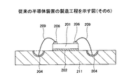
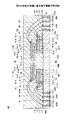
図1は、従来の半導体装置の断面図である。 FIG. 1 is a cross-sectional view of a conventional semiconductor device.
図1を参照するに、従来の半導体装置200は、半導体チップ201と、チップ固定用樹脂202と、封止樹脂203と、外部接続端子204とを有する。
Referring to FIG. 1, a
半導体チップ201は、半導体基板(図示せず)と、半導体基板上に形成された半導体集積回路(図示せず)と、半導体集積回路と電気的に接続されたパッド206とを有する。半導体基板としては、例えば、シリコン基板を用いることができる。パッド206は、ワイヤ209を介して、外部接続端子204と電気的に接続(ワイヤボンディング接続)されている。
The
チップ固定用樹脂202は、半導体チップ201の裏面201Aを覆うように設けられている。チップ固定用樹脂202としては、接着性を有した弾性率の高い樹脂を用いる。具体的には、例えば、チップ固定用樹脂202として弾性率が5GPa以上のアクリル系樹脂やエポキシ系樹脂等を用いる。
The
封止樹脂203は、半導体チップ201及びワイヤ209を覆うように設けられている。封止樹脂203は、突出部208を有する。封止樹脂203としては、弾性率の高い樹脂を用いる。具体的には、封止樹脂203としては、例えば、弾性率が10GPa以上のエポキシ系樹脂を用いる。
The sealing
外部接続端子204は、導電性を有しており、突出部208を覆うように設けられている。外部接続端子204は、マザーボード等の実装基板(図示せず)に設けられた配線パターンと電気的に接続される端子である。
The
図2〜図8は、従来の半導体装置の製造工程を示す図である。図2〜図8において、従来の半導体装置200と同一構成部分には同一符号を付す。
2 to 8 are diagrams showing a manufacturing process of a conventional semiconductor device. 2 to 8, the same components as those of the
図2〜図8を参照して、従来の半導体装置200の製造方法について説明する。始めに、図2に示す工程では、支持板となる金属板211上に開口部212Aを有したレジスト膜212を形成する。次いで、図3に示す工程では、レジスト膜212をマスクとするウエットエッチングにより、金属板211に凹部211Aを形成する。
A conventional method for manufacturing the
次いで、図4に示す工程では、金属板211を給電層とする電解めっき法により、凹部211Aに金属膜を析出させて、外部接続端子204を形成する。次いで、図5に示す工程では、レジスト膜212を除去する。
Next, in the step shown in FIG. 4, an
次いで、図6に示す工程では、接着性を有したチップ固定用樹脂202を介して、半導体チップ201を金属板211上に貼り付ける。このとき、加熱によりチップ固定用樹脂202を硬化させる。
Next, in the step shown in FIG. 6, the
次いで、図7に示す工程では、ワイヤ209を介して、外部接続端子204とパッド206とを電気的に接続(ワイヤボンディング接続)する。ワイヤ209を形成する際、図7に示す構造体は加熱される。次いで、図8に示す工程では、半導体チップ201及びワイヤ209を覆うように封止樹脂203を形成する。このとき、加熱により封止樹脂203を硬化させる。その後、金属板211を除去することで、図1に示す半導体装置200が製造される(例えば、引用文献1参照。)。
しかしながら、従来の半導体装置200では、半導体チップ201の上面側には半導体チップ201(具体的には、半導体基板(図示せず))とは異なる熱膨張係数を有する封止樹脂203が設けられており、また半導体チップ201の下面側には半導体チップ201(具体的には、半導体基板(図示せず))とは異なる熱膨張係数を有するチップ固定用樹脂202が設けられている。そのため、半導体装置200が加熱された場合や加熱された半導体装置200の温度が低下した場合、半導体装置200に反りが発生してしまうという問題があった。このように、半導体装置200に反りが発生した場合には、外部接続端子204とパッド206との間の電気的接続信頼性が低下してしまう。
However, in the
また、従来の半導体装置200の製造方法では、例えば、図6及び図7に示す工程では、図6及び図7に示す構造体が加熱されるため、金属板211と半導体チップ201との熱膨張係数の差により、図6及び図7に示す構造体が反ってしまという問題があった。また、図8に示す工程では、図8に示す構造体が加熱されるため、金属板211及び封止樹脂203と半導体チップ201との熱膨張係数の差により、図8に示す構造体が反ってしまという問題があった。このように半導体装置200の製造時において反りが発生した場合、外部接続端子204とパッド206との間の電気的接続信頼性が低下して、半導体装置200の歩留まりが低下してしまう。
Further, in the conventional method for manufacturing the
そこで本発明は、上述した問題点に鑑みなされたものであり、反りの発生を抑制することのできる半導体装置、電子部品、及び半導体装置の製造方法を提供することを目的とする。 Therefore, the present invention has been made in view of the above-described problems, and an object thereof is to provide a semiconductor device, an electronic component, and a method for manufacturing the semiconductor device that can suppress the occurrence of warpage.
本発明の一観点によれば、第1の半導体チップと、前記第1の半導体チップ上に積み重ねられた第2の半導体チップと、前記第1及び第2の半導体チップを覆うように封止する第1の封止樹脂と、を備えた半導体装置であって、前記第1の封止樹脂は、低弾性樹脂であることを特徴とする半導体装置が提供される。 According to one aspect of the present invention, the first semiconductor chip, the second semiconductor chip stacked on the first semiconductor chip, and the first and second semiconductor chips are sealed. There is provided a semiconductor device comprising: a first sealing resin, wherein the first sealing resin is a low-elasticity resin.
本発明によれば、第1及び第2の半導体チップを覆うように低弾性樹脂を設けることにより、熱膨張係数の異なる低弾性樹脂と第1及び第2の半導体チップとの間に発生する応力が緩和されるため、半導体装置に反りが発生することを抑制できる。 According to the present invention, by providing the low elastic resin so as to cover the first and second semiconductor chips, the stress generated between the low elastic resin having different thermal expansion coefficients and the first and second semiconductor chips. Is mitigated, so that the semiconductor device can be prevented from warping.
本発明の他の観点によれば、第1の半導体チップと、前記第1の半導体チップ上に積み重ねられた第2の半導体チップと、前記第1の半導体チップが電気的に接続される第1の外部接続端子と、前記第2の半導体チップが電気的に接続される第2の外部接続端子と、を備えた半導体装置の製造方法であって、支持板となる金属板上に第1及び第2の外部接続端子を形成する外部接続端子形成工程と、第1の低弾性樹脂を介して、前記金属板上に前記第1の半導体チップを貼り付ける第1の半導体チップ貼付工程と、前記第1の半導体チップ上に第2の半導体チップを貼り付ける第2の半導体チップ貼付工程と、前記第1及び第2の半導体チップを第2の低弾性樹脂で封止する封止工程とを含むことを特徴とする半導体装置の製造方法が提供される。 According to another aspect of the present invention, a first semiconductor chip, a second semiconductor chip stacked on the first semiconductor chip, and a first electrically connected to the first semiconductor chip. And a second external connection terminal to which the second semiconductor chip is electrically connected, wherein the first and second external connection terminals are formed on a metal plate serving as a support plate. An external connection terminal forming step of forming a second external connection terminal, a first semiconductor chip attaching step of attaching the first semiconductor chip on the metal plate via a first low-elasticity resin, A second semiconductor chip attaching step for attaching a second semiconductor chip on the first semiconductor chip; and a sealing step for sealing the first and second semiconductor chips with a second low-elasticity resin. A method of manufacturing a semiconductor device is provided. That.
本発明によれば、金属板上に第1の低弾性樹脂を介して、第1の半導体チップを貼り付けることにより、熱膨張係数の異なる第1の半導体チップと金属板との間に発生する応力を第1の低弾性樹脂が緩和するため、反りの発生を抑制することができる。 According to the present invention, the first semiconductor chip is pasted on the metal plate via the first low-elasticity resin, and is generated between the first semiconductor chip having a different thermal expansion coefficient and the metal plate. Since the first low-elasticity resin relaxes the stress, the occurrence of warping can be suppressed.
また、第2の低弾性樹脂により第1及び第2の半導体チップを封止することで、さらに反りの発生を抑制することができる。 Further, the occurrence of warpage can be further suppressed by sealing the first and second semiconductor chips with the second low-elasticity resin.
本発明によれば、半導体装置の製造時における反りの発生を抑制することができると共に、製造後の半導体装置の反りの発生を抑制することができる。 ADVANTAGE OF THE INVENTION According to this invention, generation | occurrence | production of the curvature at the time of manufacture of a semiconductor device can be suppressed, and generation | occurence | production of the curvature of the semiconductor device after manufacture can be suppressed.
次に、図面に基づいて本発明の実施の形態について説明する。
(第1の実施の形態)
図9は、本発明の第1の実施の形態に係る半導体装置の断面図である。
Next, embodiments of the present invention will be described with reference to the drawings.
(First embodiment)
FIG. 9 is a cross-sectional view of the semiconductor device according to the first embodiment of the present invention.
図9を参照するに、第1の実施の形態の半導体装置10は、第1の半導体チップ11と、第2の半導体チップ12と、第1の低弾性樹脂13と、第2の低弾性樹脂15と、第1の外部接続端子16と、第2の外部接続端子17と、ワイヤ21,22とを有する。
Referring to FIG. 9, the
第1の半導体チップ11は、半導体基板(図示せず)と、半導体基板(図示せず)上に形成された半導体集積回路(図示せず)と、パッド24とを有する。半導体基板としては、例えば、シリコン基板を用いることができる。パッド24は、半導体集積回路(図示せず)と電気的に接続されている。パッド24は、ワイヤ21を介して、第1の外部接続端子16と電気的に接続(ワイヤボンディング接続)されている。
The
第2の半導体チップ12は、第1の半導体チップ11に設けられたパッド24と重ならないように、チップ固定用樹脂14を介して、第1の半導体チップ11上に貼り付けられている。このように、第1の半導体チップ11上に第2の半導体チップ12を積み重ねることにより、半導体装置10を小型化することができる。チップ固定用樹脂14としては、例えば、ダイアタッチフィルムを用いることができる。
The
第2の半導体チップ12は、半導体基板(図示せず)と、半導体基板(図示せず)上に形成された半導体集積回路(図示せず)と、パッド25とを有する。半導体基板としては、例えば、シリコン基板を用いることができる。パッド25は、半導体集積回路(図示せず)と電気的に接続されている。パッド25は、ワイヤ22を介して、第2の外部接続端子17と電気的に接続(ワイヤボンディング接続)されている。
The
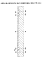
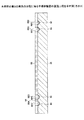
図10及び図11は、第1の半導体チップと第2の半導体チップとの位置関係を説明するための図である。 10 and 11 are diagrams for explaining the positional relationship between the first semiconductor chip and the second semiconductor chip.
例えば、第1の半導体チップ11の一辺にのみパッド24が設けられている場合、第2の半導体チップ12は、第1の半導体チップ11に対して図10に示すように配置することができる。また、第1の半導体チップ11の二辺にパッド24が設けられている場合、第2の半導体チップ12は、第1の半導体チップ11に対して図11に示すように配置することができる。
For example, when the
図2を参照するに、第1の低弾性樹脂13は、第1の半導体チップ11の下面11Aを覆うように設けられている。第1の半導体チップ11の一部(この場合、半導体チップ11の下面11A側)を封止している。第1の低弾性樹脂13の下面13Aは、第2の低弾性樹脂15の下面15Aと略面一とされている。
Referring to FIG. 2, the first low-
第1の低弾性樹脂13は、弾性率の低い樹脂であり、応力を緩和させる機能を有する。また、第1の低弾性樹脂13は、接着剤としての機能を有する。第1の低弾性樹脂13としては、例えば、弾性率が1MPa〜1GPaの樹脂を用いることができる。弾性率が1MPaよりも小さい樹脂を用いた場合、樹脂が柔らかすぎて半導体装置10の製造時における取り扱いが困難である。また、弾性率が1GPaよりも大きい樹脂を用いた場合、半導体装置10に発生する反りを抑制する効果が小さい。具体的には、第1の低弾性樹脂13としては、例えば、エラストマーを用いることができる。また、第1の低弾性樹脂13の厚さは、例えば、0.025mmとすることができる。
The first low-
第2の低弾性樹脂15は、第1の低弾性樹脂13と共に、第1及び第2の半導体チップ11,12とワイヤ21,22とを封止している。これにより、第1及び第2の半導体チップ11,12は、第1及び第2の低弾性樹脂13,15により覆われる。本実施の形態では、第1及び第2の低弾性樹脂13,15により第1の封止樹脂が構成されている。第2の低弾性樹脂15の下面15Aは、第1の低弾性樹脂の下面13Aと略面一とされている。第2の低弾性樹脂15は、弾性率の低い樹脂であり、応力を緩和させる機能を有する。
The second low-
第2の低弾性樹脂15としては、例えば、弾性率が1MPa〜1GPaの樹脂を用いることができる。弾性率が1MPaよりも小さい樹脂を用いた場合、樹脂が柔らかすぎて半導体装置10の製造時における取り扱いが困難である。また、弾性率が1GPaよりも大きい樹脂を用いた場合、半導体装置10に発生する反りを抑制する効果が小さい。具体的には、第2の低弾性樹脂15としては、例えば、エラストマーを用いることができる。
As the second low-
このように、積み重ねられた第1及び第2の半導体チップ11,12を第1及び第2の低弾性樹脂13,15で覆うことにより、熱膨張係数の異なる第1及び第2の低弾性樹脂13,15と第1及び第2の半導体チップ11,12(具体的には、第1及び第2の半導体チップ11,12に設けられた半導体基板(図示せず))との間に発生する応力が緩和されるため、半導体装置10に反りが発生することを抑制できる。これにより、第1の外部接続端子16とパッド24との接続信頼性、及び第2の外部接続端子17と第2のパッド25との接続信頼性を十分に確保することができる。
As described above, the first and second low-elasticity resins having different thermal expansion coefficients are obtained by covering the stacked first and
第1の外部接続端子16は、第2の低弾性樹脂15の下面15A側に設けられている。第1の外部接続端子16の上面16Aは、ワイヤ21と接続されている。これにより、第1の外部接続端子16は、第1の半導体チップ11と電気的に接続される。第1の外部接続端子16の下面16Bは、第2の低弾性樹脂15から露出されている。第1の外部接続端子16の下面16Bは、半導体装置10を実装基板(図示せず)に実装する際、実装基板の配線パターン(図示せず)と電気的に接続される(図32参照)。
The first
第2の外部接続端子17は、第2の低弾性樹脂15の下面15A側に設けられている。第2の外部接続端子17の上面17Aは、ワイヤ22と接続されている。これにより、第2の外部接続端子17は、第2の半導体チップ12と電気的に接続される。第2の外部接続端子17の下面17Bは、第2の低弾性樹脂15から露出されている。第2の外部接続端子17の下面17Bは、半導体装置10を実装基板(図示せず)に実装する際、実装基板の配線パターン(図示せず)と電気的に接続される(図32参照)。
The second
ワイヤ21は、第2の低弾性樹脂15により封止されている。ワイヤ21の一方の端部はパッド24と接続されており、ワイヤ21の他方の端部は第1の外部接続端子16と接続されている。
The
ワイヤ22は、第2の低弾性樹脂15により封止されている。ワイヤ22の一方の端部はパッド25と接続されており、ワイヤ22の他方の端部は第2の外部接続端子17と接続されている。
The
本実施の形態の半導体装置によれば、積み重ねられた第1及び第2の半導体チップ11,12を第1及び第2の低弾性樹脂13,15で覆うことにより、熱膨張係数の異なる第1及び第2の低弾性樹脂13,15と第1及び第2の半導体チップ11,12(具体的には、第1及び第2の半導体チップ11,12に設けられた半導体基板(図示せず))との間に発生する応力が緩和されるため、半導体装置10に反りが発生することを抑制できる。これにより、第1の外部接続端子16とパッド24との接続信頼性、及び第2の外部接続端子17と第2のパッド25との接続信頼性を十分に確保することができる。
According to the semiconductor device of the present embodiment, the first and
なお、本実施の形態の半導体装置では、チップ固定用樹脂14として、ダイアタッチフィルムを用いた場合を例に挙げて説明したが、チップ固定用樹脂14として、先に説明した第1の低弾性樹脂13を用いてもよい。チップ固定用樹脂14として第1の低弾性樹脂13を用いることにより、反りの抑制効果を向上させることができる。
In the semiconductor device of the present embodiment, the case where a die attach film is used as the
図12は、本発明の第1の実施の形態の第1変形例に係る半導体装置の断面図である。図12において、第1の実施の形態の半導体装置10と同一構成部分には同一符号を付す。
FIG. 12 is a cross-sectional view of a semiconductor device according to a first modification of the first embodiment of the present invention. In FIG. 12, the same components as those of the
図12を参照するに、第1の実施の形態の第1変形例に係る半導体装置30は、第1の実施の形態の半導体装置10に設けられた第1及び第2の外部接続端子16,17の代わりに外部接続端子31を設けた以外は半導体装置10と同様に構成される。
Referring to FIG. 12, the
外部接続端子31は、第2の低弾性樹脂15の下面15A側に設けられている。外部接続端子31の上面31Aは、ワイヤ21,22と接続されている。これにより、外部接続端子31は、第1及び第2の半導体チップ11,12と電気的に接続される。外部接続端子31の下面31Bは、第2の低弾性樹脂15から露出されている。外部接続端子31の下面31Bは、半導体装置30を実装基板(図示せず)に実装する際、実装基板の配線パターン(図示せず)と電気的に接続される。
The
このような構成とされた第1の実施の形態の第1変形例に係る半導体装置30においても、第1の実施の形態の半導体装置10と同様な効果を得ることができる。
Also in the
図13は、本発明の第1の実施の形態の第2変形例に係る半導体装置の断面図である。図13において、第1の実施の形態の半導体装置10と同一構成部分には同一符号を付す。
FIG. 13 is a cross-sectional view of a semiconductor device according to a second modification of the first embodiment of the present invention. In FIG. 13, the same components as those of the
図13を参照するに、第1の実施の形態の第2変形例に係る半導体装置40は、第1の実施の形態の半導体装置10の構成にさらに、第1の半導体チップ11と、第2の半導体チップ12と、第1の低弾性樹脂13と、第1の外部接続端子16と、第2の外部接続端子17と、ワイヤ21,22とを設けた以外は、半導体装置10と同様に構成されている。半導体装置40は、積み重ねられた第1及び第2の半導体チップ11,12を2組備えた構成とされている。
Referring to FIG. 13, the
このような構成とされた第1の実施の形態の第2変形例に係る半導体装置40においても、第1の実施の形態の半導体装置10と同様な効果を得ることができる。
Also in the
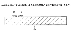
図14〜図21は、本発明の第1の実施の形態に係る半導体装置の製造工程を示す図である。図14〜図21において、第1の実施の形態の半導体装置10と同一構成部分には同一符号を付す。
14 to 21 are views showing manufacturing steps of the semiconductor device according to the first embodiment of the present invention. 14 to 21, the same components as those of the
図14〜図21を参照して、本発明の第1の実施の形態に係る半導体装置10の製造方法について説明する。
A method for manufacturing the
始めに、図14を示す工程では、支持板となる金属板45上に、開口部46A,46Bを有したレジスト膜46を形成する。金属板45の材料としては、例えば、Cuや42アロイ等を用いることができる。開口部46Aは、第1の外部接続端子16の形成位置に対応しており、開口部46Bは、第2の外部接続端子17の形成位置に対応している。
First, in the step shown in FIG. 14, a resist
次いで、図15に示す工程では、金属板45を給電層とする電解めっき法により、開口部46A,46Bに露出された金属板45上に導電金属を析出させて、第1及び第2の外部接続端子16,17を同時に形成する(外部接続端子形成工程)。
Next, in the step shown in FIG. 15, a conductive metal is deposited on the
具体的には、例えば、開口部46A,46Bに露出された金属板45上に、電解めっき法によりAu層、Ni層、Au層を順次析出させて、Au層/Ni層/Au層よりなる第1及び第2の外部接続端子16,17を同時に形成する。
Specifically, for example, an Au layer, a Ni layer, and an Au layer are sequentially deposited on the
次いで、図16に示す工程では、レジスト膜46を除去する。次いで、図17に示す工程では、第1の低弾性樹脂13を介して、第1の半導体チップ11を金属板45上に貼り付ける(第1の半導体チップ貼付工程)。
Next, in the step shown in FIG. 16, the resist
第1の低弾性樹脂13は、弾性率の低い樹脂であり、応力を緩和させる機能を有する。また、第1の低弾性樹脂13は、接着剤としての機能を有する。第1の低弾性樹脂13としては、例えば、弾性率が1MPa〜1GPaの樹脂を用いることができる。弾性率が1MPaよりも小さい樹脂を用いた場合、樹脂が柔らかすぎて半導体装置10の製造時における取り扱いが困難である。また、弾性率が1GPaよりも大きい樹脂を用いた場合、半導体装置10に発生する反りを抑制する効果が小さい。具体的には、第1の低弾性樹脂13としては、例えば、エラストマーを用いることができる。
The first low-
このように、応力を緩和させる機能を有する第1の低弾性樹脂13を介して、金属板45上に第1の半導体チップ11を貼り付けることにより、熱膨張係数の異なる第1の半導体チップ11と金属板45との間に第1の低弾性樹脂13が配設される。これにより、金属板45と第1の半導体チップ11との間で応力が発生した場合、第1の低弾性樹脂13により応力が緩和されるため、半導体装置10の製造時における反りの発生を抑制することができる。
Thus, by sticking the
次いで、図18に示す工程では、第1の半導体チップ11上にチップ固定用樹脂14を介して、第2の半導体チップ12を貼り付ける(第2の半導体チップ貼付工程)。このとき、第2の半導体チップ12は、第1の半導体チップ11に設けられたパッド24と重ならないように貼り付ける。このように、第2の半導体チップ12をパッド24と重ならないように第1の半導体チップ11上に貼り付けることで、ワイヤ21を介して、第1の半導体チップ11と第1の外部接続端子16とを電気的に接続することができる。チップ固定用樹脂14としては、ダイアタッチフィルムを用いることができる。
Next, in the step shown in FIG. 18, the
次いで、図19に示す工程では、ワイヤ21を介して、第1の半導体チップ11のパッド24と第1の外部接続端子16とを電気的に接続すると共に、ワイヤ22を介して、第2の半導体チップ12のパッド25と第2の外部接続端子17とを電気的に接続する。これにより、第1の半導体チップ11は、第1の外部接続端子16に対してワイヤボンディング接続され、第2の半導体チップ12は、第2の外部接続端子17に対してワイヤボンディング接続される。
Next, in the step shown in FIG. 19, the
次いで、図20に示す工程では、第1及び第2の半導体チップ11,12と、ワイヤ21,22と、第1及び第2の外部接続端子16,17とを覆うように第2の低弾性樹脂15を形成する(封止工程)。これにより、第1及び第2の半導体チップ11,12及びワイヤ21,22は、第1及び第2の低弾性樹脂13,15により封止される。
Next, in the step shown in FIG. 20, the second low elasticity so as to cover the first and
第2の低弾性樹脂15としては、例えば、弾性率が1MPa〜1GPaの樹脂を用いることができる。弾性率が1MPaよりも小さい樹脂を用いた場合、樹脂が柔らかすぎて半導体装置10の製造時における取り扱いが困難である。また、弾性率が1GPaよりも大きい樹脂を用いた場合、半導体装置10に発生する反りを抑制する効果が小さい。具体的には、第2の低弾性樹脂15としては、例えば、エラストマーを用いることができる。
As the second low-
このように、応力を緩和させる機能を有する第1及び第2の低弾性樹脂13,15により、第1及び第2の半導体チップ11,12及びワイヤ21,22を封止することにより、図20に示す構造体に応力が発生した場合、第1及び第2の低弾性樹脂13,15により応力が緩和されるので、半導体装置10の製造時における反りの発生を抑制することができる。これにより、第1の半導体チップ11と第1の外部接続端子16との間の電気的接続信頼性、及び第2の半導体チップ12と第2の外部接続端子17との間の電気的接続信頼性を向上させることができる。
Thus, by sealing the first and
次いで、図21に示す工程では、金属板45をエッチングにより除去する。これにより、半導体装置10が製造される。
Next, in the step shown in FIG. 21, the
本実施の形態の半導体装置の製造方法によれば、応力を緩和させる機能を有する第1の低弾性樹脂13を介して、金属板45上に第1の半導体チップ11を貼り付けることにより、熱膨張係数の異なる第1の半導体チップ11と金属板45との間で応力が発生した場合、第1の低弾性樹脂13により応力を緩和して、反りの発生を抑制することができる。
According to the method for manufacturing a semiconductor device of the present embodiment, the
また、応力を緩和させる機能を有する第1及び第2の低弾性樹脂13,15により、第1及び第2の半導体チップ11,12とワイヤ21,22とを封止することで、図20に示す構造体に応力が発生した場合、第1及び第2の低弾性樹脂13,15により応力を緩和して、反りの発生を抑制することができる。
Further, by sealing the first and
なお、本実施の形態では、金属板45上に1つの半導体装置10を製造する場合を例に挙げて説明したが、金属板45上に複数の半導体装置10を形成し、次いで、複数の半導体装置10を個片化し、その後、金属板45を除去して、複数の半導体装置10を製造してもよい。
In the present embodiment, the case where one
(第2の実施の形態)
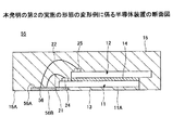
図22は、本発明の第2の実施の形態に係る半導体装置の断面図である。図22において、第1の実施の形態の半導体装置10と同一構成部分には同一符号を付す。
(Second Embodiment)
FIG. 22 is a sectional view of a semiconductor device according to the second embodiment of the present invention. In FIG. 22, the same components as those of the
図22を参照するに、第2の実施の形態の半導体装置50は、第1の実施の形態の半導体装置10に設けられた第1及び第2の外部接続端子16,17の代わりに、第1及び第2の外部接続端子51,52を設けた以外は、第1の実施の形態の半導体装置10と同様に構成される。
Referring to FIG. 22, the
図23は、第1及び第2の外部接続端子と第1の半導体チップとの位置関係を説明するための図である。 FIG. 23 is a diagram for explaining the positional relationship between the first and second external connection terminals and the first semiconductor chip.
図22及び図23を参照して、第1及び第2の外部接続端子51,52について説明する。第1及び第2の外部接続端子51,52は、交互に配置されている。第1及び第2の外部接続端子51,52は、第2の低弾性樹脂15により封止されている。第1及び第2の外部接続端子51,52の下面51B,52Bは、第2の低弾性樹脂15から露出されている。第1及び第2の外部接続端子51,52の下面51B,52Bは、第2の低弾性樹脂15の下面15Aと略面一とされている。
The first and second
第1の外部接続端子51は、その一部が第1の半導体チップ11の下面11Bと接触している。このように、第1の外部接続端子51の一部を第1の半導体チップ11の下面11Bと接触させることにより、第1の半導体チップ11が支持板となるため、第1の半導体チップ11の下面11Bと接触する部分の第1の外部接続端子51の変位量を小さくすることができる。
A part of the first
第1の外部接続端子51の上面51Aは、ワイヤ21を介して、第1の半導体チップ11と電気的に接続されている。実装基板(図示せず)に半導体装置50を実装する場合、第1の半導体チップ11の下面11Bと接触する部分の第1の外部接続端子51に実装基板の配線パターン(図示せず)と接続されたワイヤ(図示せず)が接続される(図33参照)。
The
第2の外部接続端子52は、その一部が第1の半導体チップ11の下面11Bと接触している。このように、第2の外部接続端子52の一部を第1の半導体チップ11の下面11Bと接触させることにより、第1の半導体チップ11が支持板となるため、第1の半導体チップ11の下面11Bと接触する部分の第2の外部接続端子52の変位量を小さくすることができる。
A part of the second
第2の外部接続端子52の上面52Aは、ワイヤ22を介して、第2の半導体チップ12と電気的に接続されている。実装基板(図示せず)に半導体装置50を実装する場合、第1の半導体チップ11の下面11Bと接触する部分の第2の外部接続端子52に実装基板の配線パターン(図示せず)と接続されたワイヤ(図示せず)が接続される(図33参照)。
The
本実施の形態の半導体装置によれば、第1及び第2の外部接続端子51,52の一部が第1の半導体チップ11の下面11Bと接触するように第1及び第2の外部接続端子51,52を配置することにより、実装基板(図示せず)に半導体装置50を実装する場合、第1の半導体チップ11の下面11Bと接触する部分の第1及び第2の外部接続端子51,52(変位量の少ない第1及び第2の外部接続端子51,52部分)に実装基板と電気的に接続されたワイヤ(図示せず)を接続することが可能となる。これにより、第1及び第2の外部接続端子51,52と実装基板と接続されたワイヤ(図示せず)との間の接続信頼性を向上させることができる。
According to the semiconductor device of the present embodiment, the first and second external connection terminals are such that a part of the first and second
第2の実施の形態の半導体装置50は、第1の実施の形態で説明した図17に示す工程において、第1の半導体チップ11の下面11Aが第1及び第2の外部接続端子51,52の上面51A,52Aの一部と接触するように、第1の半導体チップ11を金属板45上に貼り付ける以外は、第1の実施の形態の半導体装置10の製造方法と同様な手法により製造することができる。
In the
図24は、本発明の第2の実施の形態の変形例に係る半導体装置の断面図である。図24において、第2の実施の形態の半導体装置50と同一構成部分には同一符号を付す。
FIG. 24 is a cross-sectional view of a semiconductor device according to a modification of the second embodiment of the present invention. In FIG. 24, the same components as those of the
図24を参照するに、第2の実施の形態の変形例に係る半導体装置55は、第2の実施の形態の半導体装置50に設けられた第1及び第2の外部接続端子51,52の代わりに外部接続端子56を設けた以外は、半導体装置50と同様に構成される。
Referring to FIG. 24, a
外部接続端子56は、第2の低弾性樹脂15により封止されている。外部接続端子56は、その一部が第1の半導体チップ11の下面11Bと接触するように配置されている。外部接続端子56の上面56Aは、ワイヤ21,22を介して、第1及び第2の半導体チップ11,12と電気的に接続されている。外部接続端子56の下面56Bは、第2の低弾性樹脂15から露出されている。外部接続端子56の下面56Bは、第2の低弾性樹脂15の下面15Aと略面一とされている。
The
実装基板(図示せず)に半導体装置55を実装する場合、第1の半導体チップ11の下面11Bと接触する部分の外部接続端子56に実装基板の配線パターン(図示せず)と接続されたワイヤ(図示せず)が接続される。
When the
このような構成とされた第2の実施の形態の変形例に係る半導体装置55においても、第2の実施の形態の半導体装置50と同様な効果を得ることができる。
Also in the
また、第2の実施の形態の変形例に係る半導体装置55は、第2の実施の形態の半導体装置50と同様な手法により製造することができ、第1の実施の形態の半導体装置10の製造方法と同様な効果を得ることができる。
Further, the
(第3の実施の形態)
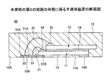
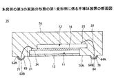
図25は、本発明の第3の実施の形態に係る半導体装置の断面図である。図25において、第1の実施の形態の半導体装置10と同一構成部分には同一符号を付す。
(Third embodiment)
FIG. 25 is a sectional view of a semiconductor device according to the third embodiment of the present invention. In FIG. 25, the same components as those of the
図25を参照するに、第3の実施の形態の半導体装置60は、第1の実施の形態の半導体装置10に設けられた第2の低弾性樹脂15と第1及び第2の外部接続端子16,17との代わりに、第2の低弾性樹脂61、第1及び第2の外部接続端子63,64、及びダミー用接続端子65,66を設けた以外は、半導体装置10と同様に構成される。
Referring to FIG. 25, the
第2の低弾性樹脂61は、弾性率の低い樹脂であり、応力を緩和させる機能を有する。第2の低弾性樹脂61としては、例えば、弾性率が1MPa〜1GPaの樹脂を用いることができる。弾性率が1MPaよりも小さい樹脂を用いた場合、樹脂が柔らかすぎて半導体装置60の製造時における取り扱いが困難である。また、弾性率が1GPaよりも大きい樹脂を用いた場合、半導体装置60に発生する反りを抑制する効果が小さい。具体的には、第2の低弾性樹脂61としては、例えば、エラストマーを用いることができる。
The second low-
第2の低弾性樹脂61は、第1の低弾性樹脂13と共に、第1及び第2の半導体チップ11,12とワイヤ21,22とを封止している。
The second low-
このように、積み重ねられた第1及び第2の半導体チップ11,12を第1及び第2の低弾性樹脂13,61で覆うことにより、熱膨張係数の異なる第1及び第2の低弾性樹脂13,61と第1及び第2の半導体チップ11,12(具体的には、第1及び第2の半導体チップ11,12に設けられた半導体基板(図示せず))との間に発生する応力が緩和されるため、半導体装置60に反りが発生することを抑制できる。これにより、第1の外部接続端子63とパッド24との接続信頼性、及び第2の外部接続端子64と第2のパッド25との接続信頼性を十分に確保することができる。
Thus, the 1st and 2nd low elastic resin from which a thermal expansion coefficient differs is covered by covering the 1st and
第2の低弾性樹脂61は、その下面61Aから突出する複数の突出部67,68,71,72を有する。突出部67,68,71,72の形状は、例えば、半球形状とすることができる。
The second low-
第1の外部接続端子63は、突出部67を覆うように設けられている。第1の外部接続端子63の内面63Aは、ワイヤ21を介して、第1の半導体チップ11のパッド24と電気的に接続されている。第1の外部接続端子63の外面63Bは、半導体装置60をマザーボード等の実装基板(図示せず)に実装する際、実装基板のパッド(図示せず)と電気的に接続される。
The first
第2の外部接続端子64は、突出部68を覆うように設けられている。第2の外部接続端子64の内面64Aは、ワイヤ22を介して、第2の半導体チップ12のパッド25と電気的に接続されている。第2の外部接続端子64の外面64Bは、半導体装置60をマザーボード等の実装基板(図示せず)に実装する際、実装基板のパッド(図示せず)と電気的に接続される。第1及び第2の外部接続端子63,64としては、例えば、Au/Ni/Au積層膜を用いることができる。
The second
ダミー用接続端子65は、突出部71を覆うように設けられている。ダミー用接続端子66は、突出部72を覆うように設けられている。半導体装置60をマザーボード等の実装基板(図示せず)に実装する場合、ダミー用接続端子65,66の外面65B,66Bは実装基板(図示せず)に設けられたダミー用のパッド(図示せず)と接続される。ダミー用のパッド(図示せず)は、実装基板(図示せず)に設けられた配線パターンと電気的に接続されていないパッドである。
The
突出部71,72及びダミー用接続端子65,66は、実装基板(図示せず)に実装された半導体装置60を実装基板(図示せず)に対して略水平となるように配置するためのものである。ダミー用接続端子65,66としては、例えば、Au/Ni/Au積層膜を用いることができる。
The
このような構成とされた第3の実施の形態の半導体装置60においても、第1の実施の形態の半導体装置10と同様な効果を得ることができる。
Also in the
図26は、本発明の第3の実施の形態の第1変形例に係る半導体装置の断面図である。図26において、第3の実施の形態の半導体装置60と同一構成部分には同一符号を付す。
FIG. 26 is a cross-sectional view of a semiconductor device according to a first modification of the third embodiment of the present invention. In FIG. 26, the same components as those of the
図26を参照するに、第3の実施の形態の第1変形例に係る半導体装置75は、第3の実施の形態の半導体装置60に設けられた第2の低弾性樹脂61及びダミー用接続端子65,66の代わりに、第2の低弾性樹脂76を設けると共に、図25に示す第2の半導体チップ12の状態から第2の半導体チップ12の向きを180度回転させた以外は、半導体装置60と同様に構成されている。
Referring to FIG. 26, the
第2の低弾性樹脂76は、弾性率の低い樹脂であり、応力を緩和させる機能を有する。第2の低弾性樹脂76としては、例えば、弾性率が1MPa〜1GPaの樹脂を用いることができる。弾性率が1MPaよりも小さい樹脂を用いた場合、樹脂が柔らかすぎて半導体装置75の製造時における取り扱いが困難である。また、弾性率が1GPaよりも大きい樹脂を用いた場合、半導体装置75に発生する反りを抑制する効果が小さい。具体的には、第2の低弾性樹脂76としては、例えば、エラストマーを用いることができる。
The second low-
第2の低弾性樹脂76は、第1の低弾性樹脂13と共に、第1及び第2の半導体チップ11,12とワイヤ21,22とを封止している。第2の低弾性樹脂76は、その下面76Aから突出する突出部77,78を有する。突出部78は、第1の半導体チップ11を挟んで、突出部77と対向するように配置されている。第1の外部接続端子63は、突出部77を覆うように設けられている。第2の外部接続端子64は、突出部78を覆うように設けられている。
The second low-
このような構成とされた第3の実施の形態の第1変形例に係る半導体装置75においても、第1の実施の形態の半導体装置10と同様な効果を得ることができる。
Also in the
図27は、本発明の第3の実施の形態の第2変形例に係る半導体装置の断面図である。図27において、第3の実施の形態の半導体装置60と同一構成部分には同一符号を付す。
FIG. 27 is a cross-sectional view of a semiconductor device according to a second modification of the third embodiment of the present invention. In FIG. 27, the same components as those of the
図27を参照するに、第3の実施の形態の第2変形例に係る半導体装置80は、第3の実施の形態の半導体装置60に設けられたダミー用接続端子65,66及び突出部71,72の代わりに、さらに第1及び第2の半導体チップ11,12、ワイヤ21,22、第1及び第2の外部接続端子63,64、及び突出部67,68を設けた以外は半導体装置60と同様な構成とされている。半導体装置80は、積み重ねられた第1及び第2の半導体チップ11,12を2組備えた構成とされている。
Referring to FIG. 27, a
このような構成とされた第3の実施の形態の第2変形例に係る半導体装置80においても、第1の実施の形態の半導体装置10と同様な効果を得ることができる。
Also in the
図28〜図31は、本発明の第3の実施の形態に係る半導体装置の製造工程を示す図である。図28〜図31において、第3の実施の形態の半導体装置60と同一構成部分には同一符号を付す。
28 to 31 are views showing a manufacturing process of the semiconductor device according to the third embodiment of the invention. 28 to 31, the same components as those of the
図28〜図31を参照して、第3の実施の形態の半導体装置60の製造方法について説明する。始めに、図28に示す工程では、支持板となる金属板85上に、開口部86A〜86Dを有したレジスト膜86を形成する。金属板85の材料としては、例えば、Cuや42アロイ等を用いることができる。開口部86A〜86Dは、突出部67,68,71,72の形成位置に対応している。
With reference to FIGS. 28 to 31, a method for manufacturing the
次いで、図29に示す工程では、レジスト膜86をマスクとして金属板85をウエットエッチングして、開口部86A〜86Dに露出された金属板85に凹部85A〜85Dを形成する。
Next, in the step shown in FIG. 29, the
次いで、図30に示す工程では、金属板85を給電層とする電解めっき法により、凹部85A〜85Dに導電金属を析出させて、第1及び第2の外部接続端子63,64とダミー用接続端子65,66とを同時に形成する(外部接続端子形成工程)。
Next, in the process shown in FIG. 30, conductive metal is deposited in the
次いで、図31に示す工程では、レジスト膜86を除去する。その後、第1の実施の形態で説明した図17〜図21に示す工程と同様な処理を行うことにより、図25に示す半導体装置60が製造される。
Next, in the step shown in FIG. 31, the resist
本実施の形態の半導体装置の製造方法においても、第1の実施の形態の半導体装置10の製造方法と同様な効果を得ることができる。
Also in the manufacturing method of the semiconductor device of the present embodiment, the same effect as that of the manufacturing method of the
(第4の実施の形態)
図32は、第4の実施の形態に係る電子装置の断面図である。
(Fourth embodiment)
FIG. 32 is a cross-sectional view of an electronic device according to the fourth embodiment.
図32を参照するに、第4の実施の形態に係る電子装置90は、実装基板91と、半導体装置10−1〜10−4と、ワイヤ94〜97,101〜104と、第2の封止樹脂である封止樹脂92とを有する。
Referring to FIG. 32, an
実装基板91は、基板本体106と、貫通ビア109A〜109Hと、第1のパッド111〜118と、第2のパッド121〜128とを有する。本実施の形態では、貫通ビア109A〜109H、第1のパッド111〜118、及び第2のパッド121〜128により実装基板91の配線パターンが構成されている。
The mounting
基板本体106は、板状とされており、複数の貫通孔107を有する。貫通ビア109A〜109Hは、貫通孔107に設けられている。
The
第1のパッド111〜118は、基板本体106の上面106Aに設けられている。第1のパッド111は、貫通ビア109Aと接続されており、第1のパッド112は、貫通ビア109Bと接続されている。第1のパッド113は、貫通ビア109Cと接続されており、第1のパッド114は、貫通ビア109Dと接続されている。第1のパッド115は、貫通ビア109Eと接続されており、第1のパッド116は、貫通ビア109Fと接続されている。第1のパッド117は、貫通ビア109Gと接続されており、第1のパッド118は、貫通ビア109Hと接続されている。
The
第2のパッド121〜128は、基板本体106の下面106Bに設けられている。第2のパッド121は、貫通ビア109Aを介して、第1のパッド111と電気的に接続されている。第2のパッド122は、貫通ビア109Bを介して、第1のパッド112と電気的に接続されている。第2のパッド123は、貫通ビア109Cを介して、第1のパッド113と電気的に接続されている。第2のパッド124は、貫通ビア109Dを介して、第1のパッド114と電気的に接続されている。第2のパッド125は、貫通ビア109Eを介して、第1のパッド115と電気的に接続されている。第2のパッド126は、貫通ビア109Fを介して、第1のパッド116と電気的に接続されている。第2のパッド127は、貫通ビア109Gを介して、第1のパッド117と電気的に接続されている。第2のパッド128は、貫通ビア109Hを介して、第1のパッド118と電気的に接続されている。実装基板91としては、例えば、マザーボードを用いることができる。
The
半導体装置10−1〜10−4は、第1の実施の形態の半導体装置10と同様な構成とされている。なお、説明の便宜上、半導体装置10−1の構成要素の符号には−1を付し、半導体装置10−2の構成要素の符号には−2を付し、半導体装置10−3の構成要素の符号には−3を付し、半導体装置10−4の構成要素の符号には−4を付して以下の説明を行う。
The semiconductor devices 10-1 to 10-4 have the same configuration as the
半導体装置10−1は、チップ固定用樹脂131を介して、基板本体106上に貼り付けられている。チップ固定用樹脂131としては、例えば、ダイアタッチフィルムを用いることができる。
The semiconductor device 10-1 is affixed onto the
半導体装置10−1は、第1の半導体チップ11−1と、第2の半導体チップ12−1と、第1の半導体チップ11−1と電気的に接続された第1の外部接続端子16−1と、第2の半導体チップ12−1と電気的に接続された第2の外部接続端子17−1と、第1及び第2の半導体チップ11−1,12−1を覆う第1及び第2の低弾性樹脂13−1,15−1とを有する。第1の外部接続端子16−1は、ワイヤ95を介して、第1のパッド113と電気的に接続されている。第2の外部接続端子17−1は、ワイヤ94を介して、第1のパッド114と電気的に接続されている。
The semiconductor device 10-1 includes a first semiconductor chip 11-1, a second semiconductor chip 12-1, and a first external connection terminal 16- electrically connected to the first semiconductor chip 11-1. 1, a second external connection terminal 17-1 electrically connected to the second semiconductor chip 12-1, and a first and a second covering the first and second semiconductor chips 11-1 and 12-1. 2 low-elasticity resins 13-1 and 15-1. The first external connection terminal 16-1 is electrically connected to the
半導体装置10−2は、チップ固定用樹脂132を介して、半導体装置10−1上に貼り付けられている。チップ固定用樹脂132としては、例えば、ダイアタッチフィルムを用いることができる。半導体装置10−2は、第1及び第2の外部接続端子16−1,17−1と重ならないように半導体装置10−1上に積み重ねられている。
The semiconductor device 10-2 is affixed on the semiconductor device 10-1 via a
半導体装置10−2は、第1の半導体チップ11−2と、第2の半導体チップ12−2と、第1の半導体チップ11−2と電気的に接続された第1の外部接続端子16−2と、第2の半導体チップ12−2と電気的に接続された第2の外部接続端子17−2と、第1及び第2の半導体チップ11−2,12−2を覆う第1及び第2の低弾性樹脂13−2,15−2とを有する。第1の外部接続端子16−2は、ワイヤ97を介して、第1のパッド111と電気的に接続されている。第2の外部接続端子17−2は、ワイヤ96を介して、第1のパッド112と電気的に接続されている。
The semiconductor device 10-2 includes a first semiconductor chip 11-2, a second semiconductor chip 12-2, and a first external connection terminal 16- electrically connected to the first semiconductor chip 11-2. 2, the second external connection terminal 17-2 electrically connected to the second semiconductor chip 12-2, and the first and second covers the first and second semiconductor chips 11-2 and 12-2. 2 low-elasticity resins 13-2 and 15-2. The first external connection terminal 16-2 is electrically connected to the
半導体装置10−3は、チップ固定用樹脂133を介して、基板本体106上に固定されている。チップ固定用樹脂133としては、例えば、ダイアタッチフィルムを用いることができる。半導体装置10−3は、第1の半導体チップ11−3と、第2の半導体チップ12−3と、第1の半導体チップ11−3と電気的に接続された第1の外部接続端子16−3と、第2の半導体チップ12−3と電気的に接続された第2の外部接続端子17−3と、第1及び第2の半導体チップ11−3,12−3を覆う第1及び第2の低弾性樹脂13−3,15−3とを有する。第1の外部接続端子16−3は、ワイヤ102を介して、第1のパッド116と電気的に接続されている。第2の外部接続端子17−3は、ワイヤ101を介して、第1のパッド115と電気的に接続されている。
The semiconductor device 10-3 is fixed on the
半導体装置10−4は、チップ固定用樹脂134を介して、半導体装置10−3上に固定されている。チップ固定用樹脂134としては、例えば、ダイアタッチフィルムを用いることができる。半導体装置10−4は、第1及び第2の外部接続端子16−3,17−3と重ならないように半導体装置10−3上に積み重ねられている。半導体装置10−4は、第1の半導体チップ11−4と、第2の半導体チップ12−4と、第1の半導体チップ11−4と電気的に接続された第1の外部接続端子16−4と、第2の半導体チップ12−4と電気的に接続された第2の外部接続端子17−4と、第1及び第2の半導体チップ11−4,12−4を覆う第1及び第2の低弾性樹脂13−4,15−4とを有する。第1の外部接続端子16−4は、ワイヤ104を介して、第1のパッド118と電気的に接続されている。第2の外部接続端子17−4は、ワイヤ103を介して、第1のパッド117と電気的に接続されている。
The semiconductor device 10-4 is fixed on the semiconductor device 10-3 via a
封止樹脂92は、半導体装置10−1〜10−4と、ワイヤ94〜97,101〜104とを封止するように実装基板91上に設けられている。封止樹脂92としては、例えば、弾性率が10GPa以上の樹脂を用いることができる。具体的には、封止樹脂92としては、例えば、モールド樹脂を用いることができる。
The sealing
本実施の形態の電子装置によれば、第1及び第2の半導体チップ11−1〜11−4,12−1〜12−4が応力を緩和する機能を有する第1及び第2の低弾性樹脂13−1〜13−4,15−1〜15−4に覆われた半導体装置10−1〜10−4を設けることにより、実装基板91と第1及び第2の半導体チップ11−1〜11−4,12−1〜12−4との間に発生する応力が緩和されるため、第1及び第2の半導体チップ11−1〜11−4,12−1〜12−4が電子装置140の反りの影響を受けにくくすることができる。
According to the electronic device of the present embodiment, the first and second semiconductor chips 11-1 to 11-4 and 12-1 to 12-4 have the first and second low elasticity functions of relieving stress. By providing the semiconductor devices 10-1 to 10-4 covered with the resins 13-1 to 13-4 and 15-1 to 15-4, the mounting
なお、本実施の形態では、チップ固定用樹脂131〜134にダイアタッチフィルムを用いた場合を例に挙げて説明したが、チップ固定用樹脂131〜134の代わりに第1の低弾性樹脂13を用いても良い。また、本実施の形態では、封止樹脂92としてモールド樹脂を用いた場合を例に挙げて説明したが、モールド樹脂の代わりに第2の低弾性樹脂15を用いても良い。このように、チップ固定用樹脂131〜134及び封止樹脂92として低弾性樹脂を用いることにより、電子装置90に発生する反りをさらに抑制することができる。
In this embodiment, the case where a die attach film is used for the
(第5の実施の形態)
図33は、第5の実施の形態に係る電子装置の断面図である。図33において、第4の実施の形態の電子装置90と同一構成部分には同一符号を付す。
(Fifth embodiment)
FIG. 33 is a cross-sectional view of an electronic device according to the fifth embodiment. In FIG. 33, the same components as those of the
図33を参照するに、第5の実施の形態に係る電子装置140は、第4の実施の形態の電子装置90に設けられた半導体装置10−1〜10−4の代わりに、半導体装置50−1〜50−4を設けた以外は電子装置90と同様に構成される。
Referring to FIG. 33, an
半導体装置50−1〜50−4は、第2の実施の形態の半導体装置50と同様な構成とされている。なお、説明の便宜上、半導体装置50−1の構成要素の符号には−1を付し、半導体装置50−2の構成要素の符号には−2を付し、半導体装置50−3の構成要素の符号には−3を付し、半導体装置50−4の構成要素の符号には−4を付して以下の説明を行う。
The semiconductor devices 50-1 to 50-4 are configured similarly to the
半導体装置50−1は、チップ固定用樹脂131を介して、基板本体106上に貼り付けられている。半導体装置50−1は、第1の半導体チップ11−1と、第2の半導体チップ12−1と、第1の半導体チップ11−1と電気的に接続された第1の外部接続端子51−1と、第2の半導体チップ12−1と電気的に接続された第2の外部接続端子52−1と、第1及び第2の半導体チップ11−1,12−1を覆う第1及び第2の低弾性樹脂13−1,15−1とを有する。第1及び第2の外部接続端子51−1,52−1は、その一部が第1の半導体チップ11−1の下面11−1Aと接触するように配置されている。第1の外部接続端子51−1は、ワイヤ95を介して、第1のパッド113と電気的に接続されている。ワイヤ95は、半導体チップ11−1の下面11−1A上に位置する第1の外部接続端子51−1と接続されている。
The semiconductor device 50-1 is affixed onto the
このように、半導体チップ11−1の下面11−1A上に位置する第1の外部接続端子51−1にワイヤ95を接続することにより、第1の半導体チップ11−1が第1の外部接続端子51−1の位置を規制する支持板となるため、ワイヤ95と第1の外部接続端子51−1との接続を強固にすることができる。
Thus, by connecting the
第2の外部接続端子52−1は、ワイヤ94を介して、第1のパッド114と電気的に接続されている。ワイヤ94は、半導体チップ11−1の下面11−1A上に位置する第2の外部接続端子52−1と接続されている。
The second external connection terminal 52-1 is electrically connected to the
このように、半導体チップ11−1の下面11−1A上に位置する第2の外部接続端子52−1にワイヤ94を接続することにより、第1の半導体チップ11−1が第2の外部接続端子52−1の位置を規制する支持板となるため、ワイヤ94と第2の外部接続端子52−1との接続を強固にすることができる。
Thus, by connecting the
半導体装置50−2は、チップ固定用樹脂132を介して、半導体装置10−1上に貼り付けられている。半導体装置50−2は、第1及び第2の外部接続端子51−1,52−1と重ならないように半導体装置50−1上に積み重ねられている。半導体装置50−2は、第1の半導体チップ11−2と、第2の半導体チップ12−2と、第1の半導体チップ11−2と電気的に接続された第1の外部接続端子51−2と、第2の半導体チップ12−2と電気的に接続された第2の外部接続端子52−2と、第1及び第2の半導体チップ11−2,12−2を覆う第1及び第2の低弾性樹脂13−2,15−2とを有する。第1及び第2の外部接続端子51−2,52−2は、少なくとも一部が第1の半導体チップ11−2の下面11−2Aと接触するように配置されている。第1の外部接続端子51−2は、ワイヤ97を介して、第1のパッド111と電気的に接続されている。ワイヤ97は、半導体チップ11−2の下面11−2A上に位置する第1の外部接続端子51−2と接続されている。
The semiconductor device 50-2 is affixed on the semiconductor device 10-1 via a
このように、半導体チップ11−2の下面11−2A上に位置する第1の外部接続端子51−2にワイヤ97を接続することにより、第1の半導体チップ11−2が第1の外部接続端子51−2の位置を規制する支持板となるため、ワイヤ97と第1の外部接続端子51−2との接続を強固にすることができる。
Thus, by connecting the
第2の外部接続端子52−2は、ワイヤ96を介して、第1のパッド112と電気的に接続されている。ワイヤ96は、半導体チップ11−2の下面11−2A上に位置する第2の外部接続端子52−2と接続されている。
The second external connection terminal 52-2 is electrically connected to the
このように、半導体チップ11−2の下面11−2A上に位置する第2の外部接続端子52−2にワイヤ96を接続することにより、第1の半導体チップ11−2が第2の外部接続端子52−2の位置を規制する支持板となるため、ワイヤ96と第2の外部接続端子52−2との接続を強固にすることができる。
Thus, by connecting the
半導体装置50−3は、チップ固定用樹脂133を介して、基板本体106上に貼り付けられている。半導体装置50−3は、第1の半導体チップ11−3と、第2の半導体チップ12−3と、第1の半導体チップ11−3と電気的に接続された第1の外部接続端子51−3と、第2の半導体チップ12−3と電気的に接続された第2の外部接続端子52−3と、第1及び第2の半導体チップ11−3,12−3を覆う第1及び第2の低弾性樹脂13−3,15−3とを有する。第1及び第2の外部接続端子51−3,52−3は、その一部が第1の半導体チップ11−3の下面11−3Aと接触するように配置されている。
The semiconductor device 50-3 is affixed on the
第1の外部接続端子51−3は、ワイヤ102を介して、第1のパッド116と電気的に接続されている。ワイヤ102は、半導体チップ11−3の下面11−3A上に位置する第1の外部接続端子51−3と接続されている。
The first external connection terminal 51-3 is electrically connected to the first pad 116 through the
このように、半導体チップ11−3の下面11−3A上に位置する第1の外部接続端子51−3にワイヤ102を接続することにより、第1の半導体チップ11−3が第1の外部接続端子51−3の位置を規制する支持板となるため、ワイヤ102と第1の外部接続端子51−3との接続を強固にすることができる。
Thus, by connecting the
第2の外部接続端子51−3は、ワイヤ101を介して、第1のパッド115と電気的に接続されている。ワイヤ101は、半導体チップ11−3の下面11−3A上に位置する第2の外部接続端子52−3と接続されている。
The second external connection terminal 51-3 is electrically connected to the
このように、半導体チップ11−3の下面11−3A上に位置する第2の外部接続端子52−3にワイヤ101を接続することにより、第1の半導体チップ11−3が第2の外部接続端子52−3の位置を規制する支持板となるため、第1の半導体チップ11−3が支持板となるため、ワイヤ101と第2の外部接続端子52−3との接続を強固にすることができる。
Thus, by connecting the
半導体装置50−4は、チップ固定用樹脂134を介して、半導体装置50−3上に固定されている。半導体装置50−4は、第1及び第2の外部接続端子51−3,52−3と重ならないように半導体装置50−3上に積み重ねられている。半導体装置50−4は、第1の半導体チップ11−4と、第2の半導体チップ12−4と、第1の半導体チップ11−4と電気的に接続された第1の外部接続端子51−4と、第2の半導体チップ12−4と電気的に接続された第2の外部接続端子52−4と、第1及び第2の半導体チップ11−4,12−4を覆う第1及び第2の低弾性樹脂13−4,15−4とを有する。
The semiconductor device 50-4 is fixed on the semiconductor device 50-3 via a
第1及び第2の外部接続端子51−4,52−4は、その一部が第1の半導体チップ11−4の下面11−4Aと接触するように配置されている。第1の外部接続端子51−4は、ワイヤ104を介して、第1のパッド118と電気的に接続されている。ワイヤ104は、半導体チップ11−4の下面11−4A上に位置する第1の外部接続端子51−4と接続されている。
The first and second external connection terminals 51-4 and 52-4 are arranged so that a part thereof is in contact with the lower surface 11-4A of the first semiconductor chip 11-4. The first external connection terminal 51-4 is electrically connected to the first pad 118 through the
このように、半導体チップ11−4の下面11−4A上に位置する第1の外部接続端子51−4にワイヤ104を接続することにより、第1の半導体チップ11−4が第1の外部接続端子51−4の位置を規制する支持板となるため、ワイヤ104と第1の外部接続端子51−4との接続を強固にすることができる。
Thus, by connecting the
第2の外部接続端子52−4は、ワイヤ103を介して、第1のパッド117と電気的に接続されている。ワイヤ103は、半導体チップ11−4の下面11−4A上に位置する第2の外部接続端子52−4と接続されている。
The second external connection terminal 52-4 is electrically connected to the first pad 117 through the
このように、半導体チップ11−4の下面11−4A上に位置する第2の外部接続端子52−4にワイヤ103を接続することにより、第1の半導体チップ11−4が第2の外部接続端子52−4の位置を規制する支持板となるため、ワイヤ103と第2の外部接続端子52−4との接続を強固にすることができる。
Thus, by connecting the
封止樹脂92は、半導体装置50−1〜50−4と、ワイヤ94〜97,101〜104とを封止するように実装基板91上に設けられている。
The sealing
本実施の形態の電子装置によれば、第1の半導体チップ11−1〜11−4の下面11−1A〜11−4Aと接触する部分の第1及び第2の外部接続端子51−1〜51−4,52−1〜52−4にワイヤ94〜97,101〜104を接続することにより、ワイヤ94〜97,101〜104と第1及び第2の外部接続端子51−1〜51−4,52−1〜52−4との接続を強固にすることができる。
According to the electronic device of the present embodiment, the first and second external connection terminals 51-1 to 51-1 in the portions that are in contact with the lower surfaces 11-1 to 11-4 A of the first semiconductor chips 11-1 to 11-4. By connecting the
また、本実施の形態の電子装置は、第4の実施の形態の電子装置90と同様な効果を得ることができる。
In addition, the electronic device of the present embodiment can obtain the same effects as the
なお、本実施の形態において、チップ固定用樹脂131〜134として第1の低弾性樹脂13を用いても良い。また、封止樹脂92として第2の低弾性樹脂15を用いても良い。
In the present embodiment, the first low-
以上、本発明の好ましい実施の形態について詳述したが、本発明はかかる特定の実施の形態に限定されるものではなく、特許請求の範囲内に記載された本発明の要旨の範囲内において、種々の変形・変更が可能である。 The preferred embodiments of the present invention have been described in detail above, but the present invention is not limited to such specific embodiments, and within the scope of the present invention described in the claims, Various modifications and changes are possible.
本発明によれば、半導体チップと、半導体チップを封止する封止樹脂とを備えた半導体装置及び電子部品に適用できる。 The present invention can be applied to a semiconductor device and an electronic component that include a semiconductor chip and a sealing resin that seals the semiconductor chip.
10,10−1〜10−4,30,40,50,50−1〜50−4,55,60,75,80 半導体装置
11,11−1〜11−4 第1の半導体チップ
11A,11−1A〜11−4A,13A,15A,16B,17B,31B,51B,52B,56B,61A,76A,106B 下面
12,12−1〜12−4 第2の半導体チップ
13,13−1〜13−4 第1の低弾性樹脂
15,15−1〜15−4,61,76 第2の低弾性樹脂
14,131〜134 チップ固定用樹脂
16,51,63,16−1〜16−4 第1の外部接続端子
16A,17A,31A,51A,52A,56A,106A 上面
17,52,64,17−1〜17−4 第2の外部接続端子
21,22,94〜97,101〜104 ワイヤ
24,25 パッド
31,56 外部接続端子
45,85 金属板
46,86 レジスト膜
46A,46B,86A〜86D 開口部
63A,64A 内面
63B〜66B 外面
65,66 ダミー用接続端子
67,68,71,72,77,78 突出部
85A〜85D 凹部
90,140 電子装置
91 実装基板
92 封止樹脂
106 基板本体
107 貫通孔
109A〜109H 貫通ビア
111〜118 第1のパッド
121〜128 第2のパッド
10, 10-1 to 10-4, 30, 40, 50, 50-1 to 50-4, 55, 60, 75, 80 Semiconductor device 11, 11-1 to 11-4 First semiconductor chip 11A, 11 -1A to 11-4A, 13A, 15A, 16B, 17B, 31B, 51B, 52B, 56B, 61A, 76A, 106B Lower surface 12, 12-1 to 12-4 Second semiconductor chip 13, 13-1 to 13 -4 First low elastic resin 15, 15-1 to 15-4, 61, 76 Second low elastic resin 14, 131 to 134 Chip fixing resin 16, 51, 63, 16-1 to 16-4 1 external connection terminal 16A, 17A, 31A, 51A, 52A, 56A, 106A upper surface 17, 52, 64, 17-1 to 17-4 second external connection terminal 21, 22, 94 to 97, 101 to 104 wires 24,2 5 Pad 31, 56 External connection terminal 45, 85 Metal plate 46, 86 Resist film 46A, 46B, 86A-86D Opening 63A, 64A Inner surface 63B-66B Outer surface 65, 66 Dummy connection terminal 67, 68, 71, 72, 77, 78 Protruding portion 85A to 85D Recessed portion 90,140 Electronic device 91 Mounting substrate 92 Sealing resin 106 Substrate body 107 Through hole 109A to 109H Through via 111 to 118 First pad 121 to 128 Second pad
Claims (7)
前記第1の半導体チップ上に積み重ねられた第2の半導体チップと、
前記第1及び第2の半導体チップを覆うように封止する第1の封止樹脂と、を備えた半導体装置であって、
前記第1の封止樹脂は、低弾性樹脂であることを特徴とする半導体装置。 A first semiconductor chip;
A second semiconductor chip stacked on the first semiconductor chip;
A first sealing resin for sealing so as to cover the first and second semiconductor chips, and a semiconductor device comprising:
The semiconductor device according to claim 1, wherein the first sealing resin is a low-elasticity resin.
前記第2の半導体チップが接続される第2の外部接続端子とを備え、
前記第1の半導体チップは、前記第1の外部接続端子と電気的に接続されるパッドを有しており、
前記第2の半導体チップは、前記パッドと重ならないように前記第1の半導体チップ上に積み重ねたことを特徴とする請求項1記載の半導体装置。 A first external connection terminal to which the first semiconductor chip is connected;
A second external connection terminal to which the second semiconductor chip is connected,
The first semiconductor chip has a pad electrically connected to the first external connection terminal,
The semiconductor device according to claim 1, wherein the second semiconductor chip is stacked on the first semiconductor chip so as not to overlap the pad.
前記半導体装置と電気的に接続される配線パターンを有する実装基板と、
前記半導体装置を封止する第2の封止樹脂とを備えたことを特徴とする電子装置。 A semiconductor device according to any one of claims 1 to 3,
A mounting substrate having a wiring pattern electrically connected to the semiconductor device;
An electronic device comprising: a second sealing resin for sealing the semiconductor device.
前記半導体装置に設けられた前記第1及び第2の外部接続端子が他の半導体装置と接触しないように前記複数の半導体装置を積み重ねたことを特徴とする請求項4記載の電子装置。 A plurality of the semiconductor devices;
5. The electronic device according to claim 4, wherein the plurality of semiconductor devices are stacked so that the first and second external connection terminals provided in the semiconductor device do not contact other semiconductor devices.
支持板となる金属板上に第1及び第2の外部接続端子を形成する外部接続端子形成工程と、
第1の低弾性樹脂を介して、前記金属板上に前記第1の半導体チップを貼り付ける第1の半導体チップ貼付工程と、
前記第1の半導体チップ上に第2の半導体チップを貼り付ける第2の半導体チップ貼付工程と、
前記第1及び第2の半導体チップを第2の低弾性樹脂で封止する封止工程とを含むことを特徴とする半導体装置の製造方法。 A first semiconductor chip; a second semiconductor chip stacked on the first semiconductor chip; a first external connection terminal to which the first semiconductor chip is electrically connected; and the second semiconductor chip. A second external connection terminal to which a semiconductor chip is electrically connected, and a manufacturing method of a semiconductor device comprising:
An external connection terminal forming step of forming first and second external connection terminals on a metal plate to be a support plate;
A first semiconductor chip attaching step of attaching the first semiconductor chip on the metal plate via a first low-elasticity resin;
A second semiconductor chip attaching step of attaching a second semiconductor chip on the first semiconductor chip;
And a sealing step of sealing the first and second semiconductor chips with a second low-elasticity resin.
前記第2の半導体チップは、前記パッドと重ならないように前記第1の半導体チップ上に貼り付けることを特徴とする請求項6記載の半導体装置の製造方法。 The first semiconductor chip has a pad electrically connected to the first external connection terminal,
The method of manufacturing a semiconductor device according to claim 6, wherein the second semiconductor chip is attached onto the first semiconductor chip so as not to overlap the pad.
Priority Applications (4)
| Application Number | Priority Date | Filing Date | Title |
|---|---|---|---|
| JP2006117074A JP2007294488A (en) | 2006-04-20 | 2006-04-20 | Semiconductor device, process for manufacturing the same and electronic component |
| KR1020070037328A KR20070104236A (en) | 2006-04-20 | 2007-04-17 | Semiconductor device, electronic apparatus and semiconductor device fabricating method |
| US11/736,926 US8525355B2 (en) | 2006-04-20 | 2007-04-18 | Semiconductor device, electronic apparatus and semiconductor device fabricating method |
| US13/368,900 US20120133056A1 (en) | 2006-04-20 | 2012-02-08 | Semiconductor device, electronic apparatus and semiconductor device fabricating method |
Applications Claiming Priority (1)
| Application Number | Priority Date | Filing Date | Title |
|---|---|---|---|
| JP2006117074A JP2007294488A (en) | 2006-04-20 | 2006-04-20 | Semiconductor device, process for manufacturing the same and electronic component |
Publications (2)
| Publication Number | Publication Date |
|---|---|
| JP2007294488A true JP2007294488A (en) | 2007-11-08 |
| JP2007294488A5 JP2007294488A5 (en) | 2009-04-09 |
Family
ID=38618728
Family Applications (1)
| Application Number | Title | Priority Date | Filing Date |
|---|---|---|---|
| JP2006117074A Pending JP2007294488A (en) | 2006-04-20 | 2006-04-20 | Semiconductor device, process for manufacturing the same and electronic component |
Country Status (3)
| Country | Link |
|---|---|
| US (2) | US8525355B2 (en) |
| JP (1) | JP2007294488A (en) |
| KR (1) | KR20070104236A (en) |
Cited By (1)
| Publication number | Priority date | Publication date | Assignee | Title |
|---|---|---|---|---|
| US8664757B2 (en) | 2010-07-12 | 2014-03-04 | Samsung Electronics Co., Ltd. | High density chip stacked package, package-on-package and method of fabricating the same |
Families Citing this family (6)
| Publication number | Priority date | Publication date | Assignee | Title |
|---|---|---|---|---|
| KR100886717B1 (en) | 2007-10-16 | 2009-03-04 | 주식회사 하이닉스반도체 | Stacked semiconductor package and method of manufacturing thereof |
| US8014166B2 (en) * | 2008-09-06 | 2011-09-06 | Broadpak Corporation | Stacking integrated circuits containing serializer and deserializer blocks using through silicon via |
| JP5918664B2 (en) * | 2012-09-10 | 2016-05-18 | 株式会社東芝 | Manufacturing method of stacked semiconductor device |
| US9368422B2 (en) * | 2012-12-20 | 2016-06-14 | Nvidia Corporation | Absorbing excess under-fill flow with a solder trench |
| JP2018101699A (en) * | 2016-12-20 | 2018-06-28 | ソニーセミコンダクタソリューションズ株式会社 | Solid-state imaging device, method of manufacturing the same, and electronic equipment |
| US20200118991A1 (en) * | 2018-10-15 | 2020-04-16 | Intel Corporation | Pre-patterned fine-pitch bond pad interposer |
Citations (6)
| Publication number | Priority date | Publication date | Assignee | Title |
|---|---|---|---|---|
| JP2001196526A (en) * | 2000-01-06 | 2001-07-19 | Seiko Epson Corp | Multi-bare chip mounted body, multichip package, semiconductor device and electronic unit |
| JP2003303919A (en) * | 2002-04-10 | 2003-10-24 | Hitachi Ltd | Semiconductor device and its manufacturing method |
| JP2004031946A (en) * | 2003-06-05 | 2004-01-29 | Nec Electronics Corp | Semiconductor device and its manufacturing method |
| WO2004034433A2 (en) * | 2002-10-08 | 2004-04-22 | Chippac, Inc. | Semiconductor stacked multi-package module having inverted second package |
| JP2004179622A (en) * | 2002-11-15 | 2004-06-24 | Renesas Technology Corp | Method for manufacturing semiconductor device |
| JP2005268533A (en) * | 2004-03-18 | 2005-09-29 | Shinko Electric Ind Co Ltd | Laminated semiconductor device |
Family Cites Families (13)
| Publication number | Priority date | Publication date | Assignee | Title |
|---|---|---|---|---|
| FR2439478A1 (en) * | 1978-10-19 | 1980-05-16 | Cii Honeywell Bull | FLAT HOUSING FOR DEVICES WITH INTEGRATED CIRCUITS |
| JP3007833B2 (en) | 1995-12-12 | 2000-02-07 | 富士通株式会社 | Semiconductor device and its manufacturing method, lead frame and its manufacturing method |
| WO1997020347A1 (en) * | 1995-11-28 | 1997-06-05 | Hitachi, Ltd. | Semiconductor device, process for producing the same, and packaged substrate |
| US6001671A (en) * | 1996-04-18 | 1999-12-14 | Tessera, Inc. | Methods for manufacturing a semiconductor package having a sacrificial layer |
| JP3638771B2 (en) * | 1997-12-22 | 2005-04-13 | 沖電気工業株式会社 | Semiconductor device |
| EP1209211B1 (en) * | 1999-06-18 | 2006-01-25 | Hitachi Chemical Company, Ltd. | Adhesive, adhesive member, circuit substrate for semiconductor mounting having adhesive member, and semiconductor device containing the same |
| US6605875B2 (en) * | 1999-12-30 | 2003-08-12 | Intel Corporation | Integrated circuit die having bond pads near adjacent sides to allow stacking of dice without regard to dice size |
| US20020125568A1 (en) * | 2000-01-14 | 2002-09-12 | Tongbi Jiang | Method Of Fabricating Chip-Scale Packages And Resulting Structures |
| JP3752949B2 (en) * | 2000-02-28 | 2006-03-08 | 日立化成工業株式会社 | Wiring substrate and semiconductor device |
| JP2002040095A (en) | 2000-07-26 | 2002-02-06 | Nec Corp | Semiconductor device and mounting method thereof |
| US6468471B1 (en) * | 2000-11-10 | 2002-10-22 | Gary K. Loda | System for, and method of, irradiating opposite sides of articles with optimal amounts of cumulative irradiation |
| US6753613B2 (en) * | 2002-03-13 | 2004-06-22 | Intel Corporation | Stacked dice standoffs |
| US7560821B2 (en) | 2005-03-24 | 2009-07-14 | Sumitomo Bakelite Company, Ltd | Area mount type semiconductor device, and die bonding resin composition and encapsulating resin composition used for the same |
-
2006
- 2006-04-20 JP JP2006117074A patent/JP2007294488A/en active Pending
-
2007
- 2007-04-17 KR KR1020070037328A patent/KR20070104236A/en not_active Application Discontinuation
- 2007-04-18 US US11/736,926 patent/US8525355B2/en active Active
-
2012
- 2012-02-08 US US13/368,900 patent/US20120133056A1/en not_active Abandoned
Patent Citations (6)
| Publication number | Priority date | Publication date | Assignee | Title |
|---|---|---|---|---|
| JP2001196526A (en) * | 2000-01-06 | 2001-07-19 | Seiko Epson Corp | Multi-bare chip mounted body, multichip package, semiconductor device and electronic unit |
| JP2003303919A (en) * | 2002-04-10 | 2003-10-24 | Hitachi Ltd | Semiconductor device and its manufacturing method |
| WO2004034433A2 (en) * | 2002-10-08 | 2004-04-22 | Chippac, Inc. | Semiconductor stacked multi-package module having inverted second package |
| JP2004179622A (en) * | 2002-11-15 | 2004-06-24 | Renesas Technology Corp | Method for manufacturing semiconductor device |
| JP2004031946A (en) * | 2003-06-05 | 2004-01-29 | Nec Electronics Corp | Semiconductor device and its manufacturing method |
| JP2005268533A (en) * | 2004-03-18 | 2005-09-29 | Shinko Electric Ind Co Ltd | Laminated semiconductor device |
Cited By (1)
| Publication number | Priority date | Publication date | Assignee | Title |
|---|---|---|---|---|
| US8664757B2 (en) | 2010-07-12 | 2014-03-04 | Samsung Electronics Co., Ltd. | High density chip stacked package, package-on-package and method of fabricating the same |
Also Published As
| Publication number | Publication date |
|---|---|
| US20120133056A1 (en) | 2012-05-31 |
| US8525355B2 (en) | 2013-09-03 |
| KR20070104236A (en) | 2007-10-25 |
| US20070246842A1 (en) | 2007-10-25 |
Similar Documents
| Publication | Publication Date | Title |
|---|---|---|
| TWI394503B (en) | Wiring board and method of manufacturing the same | |
| JP5193898B2 (en) | Semiconductor device and electronic device | |
| JP4058642B2 (en) | Semiconductor device | |
| JP4602208B2 (en) | Electronic component mounting structure and manufacturing method thereof | |
| JP5106460B2 (en) | Semiconductor device, manufacturing method thereof, and electronic device | |
| JP5535494B2 (en) | Semiconductor device | |
| JP4110189B2 (en) | Semiconductor package | |
| JP2007294488A (en) | Semiconductor device, process for manufacturing the same and electronic component | |
| US8169072B2 (en) | Semiconductor device, manufacturing method thereof, and electronic device | |
| JP4070470B2 (en) | Multilayer circuit board for semiconductor device, manufacturing method thereof, and semiconductor device | |
| WO2011024939A1 (en) | Semiconductor device and manufacturing method therefor | |
| JP2013069807A (en) | Semiconductor package and method for manufacturing the same | |
| JP2009147165A (en) | Semiconductor device | |
| JP5357239B2 (en) | WIRING BOARD, SEMICONDUCTOR DEVICE, AND WIRING BOARD MANUFACTURING METHOD | |
| JP5025399B2 (en) | Wiring board and manufacturing method thereof | |
| JP2007027381A (en) | Semiconductor device and electronic device | |
| JP2008091719A (en) | Semiconductor device | |
| WO2017006391A1 (en) | Semiconductor device | |
| JP2016025281A (en) | Semiconductor device and method for manufacturing the same | |
| JP2007149731A (en) | Wiring board, semiconductor device, and process for producing wiring board | |
| JP2008091418A (en) | Semiconductor device, and its manufacturing method | |
| JP2008078164A (en) | Semiconductor device, and manufacturing method thereof | |
| JP4647673B2 (en) | Heat dissipation type multi-hole semiconductor package | |
| JP2008147266A (en) | Semiconductor device and its manufacturing method | |
| JP2007165836A (en) | Semiconductor device |
Legal Events
| Date | Code | Title | Description |
|---|---|---|---|
| A521 | Written amendment |
Free format text: JAPANESE INTERMEDIATE CODE: A523 Effective date: 20090223 |
|
| A621 | Written request for application examination |
Free format text: JAPANESE INTERMEDIATE CODE: A621 Effective date: 20090223 |
|
| A977 | Report on retrieval |
Free format text: JAPANESE INTERMEDIATE CODE: A971007 Effective date: 20090929 |
|
| A131 | Notification of reasons for refusal |
Free format text: JAPANESE INTERMEDIATE CODE: A131 Effective date: 20111213 |
|
| A521 | Written amendment |
Free format text: JAPANESE INTERMEDIATE CODE: A523 Effective date: 20120131 |
|
| A131 | Notification of reasons for refusal |
Free format text: JAPANESE INTERMEDIATE CODE: A131 Effective date: 20120807 |
|
| A02 | Decision of refusal |
Free format text: JAPANESE INTERMEDIATE CODE: A02 Effective date: 20130312 |