JP2007271973A - Display device and electronic equipment to be mounted with same - Google Patents
Display device and electronic equipment to be mounted with same Download PDFInfo
- Publication number
- JP2007271973A JP2007271973A JP2006098011A JP2006098011A JP2007271973A JP 2007271973 A JP2007271973 A JP 2007271973A JP 2006098011 A JP2006098011 A JP 2006098011A JP 2006098011 A JP2006098011 A JP 2006098011A JP 2007271973 A JP2007271973 A JP 2007271973A
- Authority
- JP
- Japan
- Prior art keywords
- light emission
- row
- signal
- current
- display device
- Prior art date
- Legal status (The legal status is an assumption and is not a legal conclusion. Google has not performed a legal analysis and makes no representation as to the accuracy of the status listed.)
- Granted
Links
- 238000005401 electroluminescence Methods 0.000 claims description 35
- 239000011159 matrix material Substances 0.000 claims description 9
- 238000000034 method Methods 0.000 description 23
- 239000000872 buffer Substances 0.000 description 15
- 239000003990 capacitor Substances 0.000 description 5
- 238000010586 diagram Methods 0.000 description 3
- 239000003086 colorant Substances 0.000 description 2
- 238000003384 imaging method Methods 0.000 description 2
- 230000004044 response Effects 0.000 description 2
- 230000000694 effects Effects 0.000 description 1
- 230000002349 favourable effect Effects 0.000 description 1
- 230000006870 function Effects 0.000 description 1
- 230000002093 peripheral effect Effects 0.000 description 1
- 230000002123 temporal effect Effects 0.000 description 1
- 239000010409 thin film Substances 0.000 description 1
Images


Classifications
-
- G—PHYSICS
- G09—EDUCATION; CRYPTOGRAPHY; DISPLAY; ADVERTISING; SEALS
- G09G—ARRANGEMENTS OR CIRCUITS FOR CONTROL OF INDICATING DEVICES USING STATIC MEANS TO PRESENT VARIABLE INFORMATION
- G09G3/00—Control arrangements or circuits, of interest only in connection with visual indicators other than cathode-ray tubes
- G09G3/20—Control arrangements or circuits, of interest only in connection with visual indicators other than cathode-ray tubes for presentation of an assembly of a number of characters, e.g. a page, by composing the assembly by combination of individual elements arranged in a matrix no fixed position being assigned to or needed to be assigned to the individual characters or partial characters
- G09G3/22—Control arrangements or circuits, of interest only in connection with visual indicators other than cathode-ray tubes for presentation of an assembly of a number of characters, e.g. a page, by composing the assembly by combination of individual elements arranged in a matrix no fixed position being assigned to or needed to be assigned to the individual characters or partial characters using controlled light sources
- G09G3/30—Control arrangements or circuits, of interest only in connection with visual indicators other than cathode-ray tubes for presentation of an assembly of a number of characters, e.g. a page, by composing the assembly by combination of individual elements arranged in a matrix no fixed position being assigned to or needed to be assigned to the individual characters or partial characters using controlled light sources using electroluminescent panels
- G09G3/32—Control arrangements or circuits, of interest only in connection with visual indicators other than cathode-ray tubes for presentation of an assembly of a number of characters, e.g. a page, by composing the assembly by combination of individual elements arranged in a matrix no fixed position being assigned to or needed to be assigned to the individual characters or partial characters using controlled light sources using electroluminescent panels semiconductive, e.g. using light-emitting diodes [LED]
- G09G3/3208—Control arrangements or circuits, of interest only in connection with visual indicators other than cathode-ray tubes for presentation of an assembly of a number of characters, e.g. a page, by composing the assembly by combination of individual elements arranged in a matrix no fixed position being assigned to or needed to be assigned to the individual characters or partial characters using controlled light sources using electroluminescent panels semiconductive, e.g. using light-emitting diodes [LED] organic, e.g. using organic light-emitting diodes [OLED]
- G09G3/3225—Control arrangements or circuits, of interest only in connection with visual indicators other than cathode-ray tubes for presentation of an assembly of a number of characters, e.g. a page, by composing the assembly by combination of individual elements arranged in a matrix no fixed position being assigned to or needed to be assigned to the individual characters or partial characters using controlled light sources using electroluminescent panels semiconductive, e.g. using light-emitting diodes [LED] organic, e.g. using organic light-emitting diodes [OLED] using an active matrix
- G09G3/3233—Control arrangements or circuits, of interest only in connection with visual indicators other than cathode-ray tubes for presentation of an assembly of a number of characters, e.g. a page, by composing the assembly by combination of individual elements arranged in a matrix no fixed position being assigned to or needed to be assigned to the individual characters or partial characters using controlled light sources using electroluminescent panels semiconductive, e.g. using light-emitting diodes [LED] organic, e.g. using organic light-emitting diodes [OLED] using an active matrix with pixel circuitry controlling the current through the light-emitting element
-
- G—PHYSICS
- G09—EDUCATION; CRYPTOGRAPHY; DISPLAY; ADVERTISING; SEALS
- G09G—ARRANGEMENTS OR CIRCUITS FOR CONTROL OF INDICATING DEVICES USING STATIC MEANS TO PRESENT VARIABLE INFORMATION
- G09G3/00—Control arrangements or circuits, of interest only in connection with visual indicators other than cathode-ray tubes
- G09G3/20—Control arrangements or circuits, of interest only in connection with visual indicators other than cathode-ray tubes for presentation of an assembly of a number of characters, e.g. a page, by composing the assembly by combination of individual elements arranged in a matrix no fixed position being assigned to or needed to be assigned to the individual characters or partial characters
- G09G3/22—Control arrangements or circuits, of interest only in connection with visual indicators other than cathode-ray tubes for presentation of an assembly of a number of characters, e.g. a page, by composing the assembly by combination of individual elements arranged in a matrix no fixed position being assigned to or needed to be assigned to the individual characters or partial characters using controlled light sources
- G09G3/30—Control arrangements or circuits, of interest only in connection with visual indicators other than cathode-ray tubes for presentation of an assembly of a number of characters, e.g. a page, by composing the assembly by combination of individual elements arranged in a matrix no fixed position being assigned to or needed to be assigned to the individual characters or partial characters using controlled light sources using electroluminescent panels
- G09G3/32—Control arrangements or circuits, of interest only in connection with visual indicators other than cathode-ray tubes for presentation of an assembly of a number of characters, e.g. a page, by composing the assembly by combination of individual elements arranged in a matrix no fixed position being assigned to or needed to be assigned to the individual characters or partial characters using controlled light sources using electroluminescent panels semiconductive, e.g. using light-emitting diodes [LED]
- G09G3/3208—Control arrangements or circuits, of interest only in connection with visual indicators other than cathode-ray tubes for presentation of an assembly of a number of characters, e.g. a page, by composing the assembly by combination of individual elements arranged in a matrix no fixed position being assigned to or needed to be assigned to the individual characters or partial characters using controlled light sources using electroluminescent panels semiconductive, e.g. using light-emitting diodes [LED] organic, e.g. using organic light-emitting diodes [OLED]
- G09G3/3266—Details of drivers for scan electrodes
-
- G—PHYSICS
- G09—EDUCATION; CRYPTOGRAPHY; DISPLAY; ADVERTISING; SEALS
- G09G—ARRANGEMENTS OR CIRCUITS FOR CONTROL OF INDICATING DEVICES USING STATIC MEANS TO PRESENT VARIABLE INFORMATION
- G09G2300/00—Aspects of the constitution of display devices
- G09G2300/08—Active matrix structure, i.e. with use of active elements, inclusive of non-linear two terminal elements, in the pixels together with light emitting or modulating elements
- G09G2300/0809—Several active elements per pixel in active matrix panels
- G09G2300/0842—Several active elements per pixel in active matrix panels forming a memory circuit, e.g. a dynamic memory with one capacitor
- G09G2300/0861—Several active elements per pixel in active matrix panels forming a memory circuit, e.g. a dynamic memory with one capacitor with additional control of the display period without amending the charge stored in a pixel memory, e.g. by means of additional select electrodes
-
- G—PHYSICS
- G09—EDUCATION; CRYPTOGRAPHY; DISPLAY; ADVERTISING; SEALS
- G09G—ARRANGEMENTS OR CIRCUITS FOR CONTROL OF INDICATING DEVICES USING STATIC MEANS TO PRESENT VARIABLE INFORMATION
- G09G2310/00—Command of the display device
- G09G2310/02—Addressing, scanning or driving the display screen or processing steps related thereto
- G09G2310/0202—Addressing of scan or signal lines
- G09G2310/0205—Simultaneous scanning of several lines in flat panels
-
- G—PHYSICS
- G09—EDUCATION; CRYPTOGRAPHY; DISPLAY; ADVERTISING; SEALS
- G09G—ARRANGEMENTS OR CIRCUITS FOR CONTROL OF INDICATING DEVICES USING STATIC MEANS TO PRESENT VARIABLE INFORMATION
- G09G2310/00—Command of the display device
- G09G2310/02—Addressing, scanning or driving the display screen or processing steps related thereto
- G09G2310/0224—Details of interlacing
-
- G—PHYSICS
- G09—EDUCATION; CRYPTOGRAPHY; DISPLAY; ADVERTISING; SEALS
- G09G—ARRANGEMENTS OR CIRCUITS FOR CONTROL OF INDICATING DEVICES USING STATIC MEANS TO PRESENT VARIABLE INFORMATION
- G09G2320/00—Control of display operating conditions
- G09G2320/02—Improving the quality of display appearance
- G09G2320/0247—Flicker reduction other than flicker reduction circuits used for single beam cathode-ray tubes
-
- G—PHYSICS
- G09—EDUCATION; CRYPTOGRAPHY; DISPLAY; ADVERTISING; SEALS
- G09G—ARRANGEMENTS OR CIRCUITS FOR CONTROL OF INDICATING DEVICES USING STATIC MEANS TO PRESENT VARIABLE INFORMATION
- G09G3/00—Control arrangements or circuits, of interest only in connection with visual indicators other than cathode-ray tubes
- G09G3/20—Control arrangements or circuits, of interest only in connection with visual indicators other than cathode-ray tubes for presentation of an assembly of a number of characters, e.g. a page, by composing the assembly by combination of individual elements arranged in a matrix no fixed position being assigned to or needed to be assigned to the individual characters or partial characters
- G09G3/2007—Display of intermediate tones
- G09G3/2014—Display of intermediate tones by modulation of the duration of a single pulse during which the logic level remains constant
Abstract
Description
本発明は、入力される電流に応じて発光するエレクトロルミネセンス(EL)素子をマトリクス状に配置した表示装置に係り、とくに電流駆動型表示素子と電流プログラミング型の画素回路とを用いたインターレース方式で表示を行うアクティブマトリクス型表示装置それを搭載する電子機器に関する。 The present invention relates to a display device in which electroluminescence (EL) elements that emit light in response to an input current are arranged in a matrix, and in particular, an interlace method using a current-driven display element and a current programming pixel circuit. The present invention relates to an active matrix display device that performs display on an electronic device equipped with the active matrix display device.
近年、次世代ディスプレイとして発光素子を用いた自発光型のディスプレイが注目されている。その中でも電流によって発光輝度が制御される電流制御型の発光素子である有機EL素子を用いたディスプレイ、すなわち有機ELディスプレイが知られている。有機ELディスプレイには、表示領域および周辺回路に薄膜トランジスタ(TFT)を用いたアクティブマトリックス型があり、その駆動方式の1つとして画素内に形成された画素回路に画像データに応じた大きさの電流を設定して有機EL素子を発光させる電流プログラミング方式が用いられている。 In recent years, self-luminous displays using light-emitting elements have attracted attention as next-generation displays. Among them, a display using an organic EL element that is a current-controlled light-emitting element whose emission luminance is controlled by current, that is, an organic EL display is known. An organic EL display has an active matrix type using a thin film transistor (TFT) in a display region and a peripheral circuit. As one of the driving methods, an electric current of a magnitude corresponding to image data is supplied to a pixel circuit formed in a pixel. A current programming method is used in which the organic EL element emits light by setting.
図16は、EL素子を含む従来の電流プログラミング方式の画素回路の構成例を示す。 FIG. 16 shows a configuration example of a conventional current programming pixel circuit including an EL element.
図16において、P1及びP2が走査信号であり、データ信号として電流データIdataが入力される。EL素子の陽極(アノード)はTFT(M4)のドレイン端子に接続されており、陰極(カソード)は接地電位CGNDに接続されている。M1、M2、M4がP型TFTであり、M3がN型TFTである。 In FIG. 16, P1 and P2 are scanning signals, and current data Idata is input as a data signal. The anode (anode) of the EL element is connected to the drain terminal of the TFT (M4), and the cathode (cathode) is connected to the ground potential CGND. M1, M2, and M4 are P-type TFTs, and M3 is an N-type TFT.
図17は、画素回路2の駆動方法を説明するタイミングチャートである。
FIG. 17 is a timing chart illustrating a method for driving the
図17において、(a)はIdataに供給される電流データ、(b)(c)はそれぞれP1,P2に供給される走査信号である。注目する画素はi行目にあるとする。 In FIG. 17, (a) is current data supplied to Idata, and (b) and (c) are scanning signals supplied to P1 and P2, respectively. It is assumed that the pixel of interest is in the i-th row.
I(i−1)、I(i)、I(i+1)は、i−1行(1行前)、i行(対象行)、i+1行(1行後)の対象列の画素回路2に入力される電流データIdataを示す。
I (i−1), I (i), and I (i + 1) are applied to the
まず、時刻t0前の時点では、対象行の画素回路2には、走査信号P1にはLowレベルの信号が、P2にはHighレベルの信号が入力され、トランジスタM2がOFF、M3がOFF、M4がONの状態である。この状態では、対象行であるi行の画素回路2には、1行前の電流データIdataに対応するI(i−1)は入力されない。
First, at a time point before time t0, a low level signal is input to the
次いで、時刻t0では、P1にはHighレベルの信号が、P2にはLowレベルの信号が入力され、トランジスタM2、M3がON、M4はOFFとなる。この状態で、i行の画素回路2に該当行の電流データIdataに対応するI(i)が入力される。このとき、M4は導通状態でないため、EL素子には電流が流れない。入力されたIdataによりM1の電流駆動能力に応じた電圧が、M1のゲート端子と電源電位VCCの間に配置された容量C1に生じる。
Next, at time t0, a high level signal is input to P1, a low level signal is input to P2, and the transistors M2 and M3 are turned on and M4 is turned off. In this state, I (i) corresponding to the current data Idata of the corresponding row is input to the
次いで、時刻t1では、P2にHighレベルの信号が入力され、M2がOFFの状態となる。さらに、時刻t2では、P1にLowレベルの信号が入力され、M3がOFF、M4がONとなる。この状態では、M4が導通状態であるため、C1に生じた電圧により、M1の電流駆動能力に応じた電流がEL素子に供給される。これにより、供給された電流に応じた輝度でEL素子が発光する。 Next, at time t1, a high-level signal is input to P2, and M2 is turned off. Further, at time t2, a low level signal is input to P1, M3 is OFF, and M4 is ON. In this state, since M4 is in a conductive state, a current corresponding to the current driving capability of M1 is supplied to the EL element by the voltage generated in C1. As a result, the EL element emits light with a luminance corresponding to the supplied current.
しかしながら、1画素における有機EL素子に流れる電流は微小であり、特に低輝度で素子を発光させる際の電流データIdataは極めて小さい。そのため、所望の電流をプログラミングする際のデータ線の充電に非常に多くの時間が必要となり、1走査期間(時刻t0から時刻t1までのP2がLowレベル信号の期間)では不十分である。そこで、画素回路に比較的大きな電流を設定し、発光期間を制御することで輝度を制御するデューティー駆動が知られているが、ある程度高い周波数で駆動しなければフリッカーが発生してしまう。 However, the current flowing through the organic EL element in one pixel is very small, and the current data Idata when the element emits light with particularly low luminance is extremely small. Therefore, a very long time is required for charging the data line when programming a desired current, and one scanning period (P2 from time t0 to time t1 is a low level signal period) is insufficient. Therefore, duty driving is known in which the luminance is controlled by setting a relatively large current in the pixel circuit and controlling the light emission period. However, flickering occurs if the pixel circuit is not driven at a certain high frequency.
そのため、特許文献1では、2つのフィールド(奇数フィールドおよび偶数フィールド)で1フレームを構成するインターレース方式で表示を行いながら、デューティー駆動による発光期間制御を行う表示装置が提案されている。
For this reason,
図18は、特許文献1に記載の表示装置の駆動方法を説明するタイミングチャートである。
FIG. 18 is a timing chart illustrating a method for driving the display device described in
図18において、1フレーム(図中の1frame)は奇数フィールド(図中のODDfield)と偶数フィールド(図中のEVENfield)からなる。1〜mは表示装置の行番号を示している。X(1)〜X(m)は各行に対応する走査信号を示しており、Highレベル時に行を選択し、電流プログラミングを行う。Z(1)〜Z(m)は各行に対応する発光期間制御信号を示しており、Lowレベル時に画素が発光し、Highレベル時は非発光となる。奇数フィールドにおいては、奇数行のみ選択されて電流プログラミングを行い、偶数フィールドにおいては、偶数行のみ選択されて電流プログラミングを行う。
In FIG. 18, one frame (1 frame in the figure) is composed of an odd field (ODD field in the figure) and an even field (EVEN field in the figure).
こうして奇数ラインに対応する制御線と偶数ラインに対応する制御線が互いに分離されて駆動されると共にEL素子をデューティー駆動することにより、隣接したライン間の発光および非発光期間が異なるようになるので、フリッカーが除去される。
しかしながら、従来の駆動方法によって1フィールドを60Hzとした場合には、1フレームは30Hzとなる。すなわち、あるラインでの発光および非発光を繰り返す駆動周波数は30Hzとなり、フリッカーを防ぐ十分高い周波数であるとは言えない。その結果、画質の低下を招いてしまう。 However, when one field is set to 60 Hz by the conventional driving method, one frame is 30 Hz. That is, the drive frequency for repeating light emission and non-light emission in a certain line is 30 Hz, which cannot be said to be a sufficiently high frequency to prevent flicker. As a result, the image quality is degraded.
本発明は、インターレース方式で電流プログラミングを行いながら発光期間制御を行う表示装置に関し、フリッカーを抑制して良好な表示を行う表示装置の駆動方法を提供することを目的とする。 The present invention relates to a display device that performs light emission period control while performing current programming in an interlaced manner, and an object thereof is to provide a driving method of a display device that performs favorable display while suppressing flicker.
上記目的を達成するため、本発明に係る表示装置の駆動方法は、
電流に応じて発光輝度が制御される表示素子と、
電流の値が設定され、設定された電流を前記表示素子に供給する画素回路と、
前記表示素子と前記画素回路の組が行方向および列方向にマトリクス状に複数配置された画像表示部と、
前記画像表示部の行毎に設けられた走査線と、
前記画像表示部の行毎に設けられた発光期間制御線と、
前記画像表示部の行数に応じて配置され、前記画素回路が前記表示素子に供給する電流を設定する期間を制御する走査信号を前記走査線に出力し、かつ前記画素回路が前記表示素子に電流を供給する期間を制御する発光期間制御信号を前記発光期間制御線に出力する行制御回路と、
前記画像表示部の列毎に設けられたデータ線と、
前記画像表示部の列数に応じて配置され、前記画素回路が前記表示素子に供給する電流に応じたデータ信号を前記データ線に出力する列制御回路と、
を有する表示装置であって、
前記行制御回路が前記画像表示部の奇数行の前記走査線に前記走査信号を出力し、前記列制御回路が前記データ信号を前記データ線に出力して、前記画像表示部の奇数行の表示素子に供給する電流を当該表示素子の前記画素回路に設定する第1の動作と、
前記行制御回路が前記画像表示部の偶数行の前記走査線に前記走査信号を出力し、前記列制御回路が前記データ信号を前記データ線に出力して、前記画像表示部の偶数行の表示素子に供給する電流を当該表示素子の前記画素回路に設定する第2の動作とを交互に繰り返して行い、
前記第1と第2の動作の繰り返しの周期に同期して、前記繰り返し周期内に前記第1または第2の動作により電流が設定される回数の2倍以上の回数、前記行制御回路が前記画像表示部の奇数行と偶数行の前記発光期間制御線に前記発光期間制御信号を出力し、前記表示素子に、当該表示素子の前記画素回路内に設定された電流を一定期間供給することを特徴とする。
In order to achieve the above object, a method for driving a display device according to the present invention includes:
A display element whose emission luminance is controlled according to the current;
A pixel circuit in which a current value is set and the set current is supplied to the display element;
An image display unit in which a plurality of sets of the display element and the pixel circuit are arranged in a matrix in a row direction and a column direction;
A scanning line provided for each row of the image display unit;
A light emission period control line provided for each row of the image display unit;
A scanning signal that is arranged according to the number of rows of the image display unit and that controls a period for setting a current that the pixel circuit supplies to the display element is output to the scanning line, and the pixel circuit is applied to the display element. A row control circuit for outputting a light emission period control signal for controlling a period for supplying a current to the light emission period control line;
A data line provided for each column of the image display unit;
A column control circuit that is arranged according to the number of columns of the image display unit and outputs a data signal to the data line according to a current supplied from the pixel circuit to the display element;
A display device comprising:
The row control circuit outputs the scanning signal to the scanning lines in odd rows of the image display unit, and the column control circuit outputs the data signal to the data lines, thereby displaying odd rows in the image display unit. A first operation of setting a current supplied to the element to the pixel circuit of the display element;
The row control circuit outputs the scanning signal to the even-numbered scanning lines of the image display unit, and the column control circuit outputs the data signal to the data line to display even-numbered rows of the image display unit. A second operation of setting a current supplied to the element in the pixel circuit of the display element is alternately repeated,
Synchronously with the repetition cycle of the first and second operations, the row control circuit performs the number of times more than twice the number of times the current is set by the first or second operation within the repetition cycle. The light emission period control signal is output to the light emission period control lines of the odd-numbered and even-numbered lines of the image display unit, and the current set in the pixel circuit of the display element is supplied to the display element for a certain period. Features.
本発明によれば、インターレース方式で電流プログラミングを行いながらも各フィールド内に複数の発光期間を設けている。よって、1フィールドの駆動周波数を60Hzにした場合には、電流プログラミングは30Hz(各行においてフレーム毎に1回)で行われるが、発光は60Hz以上(各行においてフィールド毎に1回以上)で行うことができる。こうして、発光/非発光の駆動周波数を電流プログラミングの2倍以上にすることができるのでフリッカーの発生を抑制することが可能となる。 According to the present invention, a plurality of light emission periods are provided in each field while performing current programming in an interlaced manner. Therefore, when the driving frequency of one field is 60 Hz, current programming is performed at 30 Hz (once per frame in each row), but light emission is performed at 60 Hz or more (at least once per field in each row). Can do. In this way, the light emission / non-light emission drive frequency can be made twice or more that of current programming, so that the occurrence of flicker can be suppressed.
本発明に係る表示装置を実施するための最良の形態について具体的に説明する。本発明はEL素子を用いたアクティブマトリクス型表示装置に適用され、インターレース方式で電流プログラミングを行いながら発光期間制御を行うものである。 The best mode for carrying out the display device according to the present invention will be specifically described. The present invention is applied to an active matrix display device using an EL element, and performs light emission period control while performing current programming by an interlace method.
以下の実施例おいてはEL素子を用いた有機EL表示装置を例に挙げて説明するが、本発明の表示装置はこれに限定されるものではなく、電流信号によって各画素の表示を制御しうる装置に広く適用される。 In the following embodiments, an organic EL display device using EL elements will be described as an example. However, the display device of the present invention is not limited to this, and the display of each pixel is controlled by a current signal. Widely applied to devices that can
図1は、本実施例による表示装置の全体構成を示す。
図1において、画像表示部には、RGB原色数のEL素子と、このEL素子に入力される電流を制御するためのTFTから構成される画素回路とが画素1を構成してm行×n列の2次元状に配列されている。行数mは偶数である。
FIG. 1 shows the overall configuration of a display device according to this embodiment.
In FIG. 1, the image display unit includes a pixel circuit composed of an EL element having the number of primary colors RGB and a TFT for controlling a current input to the EL element to form a
表示領域の周辺には行制御回路3、および列制御回路4が配置されている。
A
行制御回路3の各出力端子からは走査信号P1(1)〜P1(m)、P2(1)〜P2(m)と発光期間制御信号P3(1)〜P3(m)が出力される。走査信号は走査線5を介して、発光期間制御信号は発光期間制御線6を介して、それぞれ各行の画素1のなかに設けられた画素回路(後述する図2の回路2)に入力される。発光期間制御線6は2行の画素に共通に接続されている。すなわち、第1行と第2行、第3行と第4行、第5行と第6行、第m−1行と第m行にはそれぞれ同一の発光期間制御信号が入力される。本実施例では発光期間制御線6は2行毎に共通に接続されているが、共通に接続されていなくても行制御回路3から2行毎に同一の発光期間制御信号が出力されていてもよい。
Scan signals P1 (1) to P1 (m), P2 (1) to P2 (m) and light emission period control signals P3 (1) to P3 (m) are output from the output terminals of the
列制御回路4には映像信号が入力され、各出力端子から電流データIdataが出力される。電流データIdataはデータ線7を介して各列の画素回路に入力される。
A video signal is input to the
本発明では、インターレース方式により電流プログラミングを行い、1フレームは奇数フィールド及び偶数フィールドの2つのフィールドから構成される。奇数フィールドにおいて奇数行である第1行、第3行、第5行、第m−1行の画素1を順次選択し、偶数フィールドにおいて偶数行である第2行、第4行、第6行、第m行の画素1を順次選択する。
In the present invention, current programming is performed by an interlace method, and one frame is composed of two fields, an odd field and an even field. The first row, the third row, the fifth row, and the (m−1) th row of
図2は、本実施例のEL素子を含む画素回路2の構成例を示す。
図2において、P1及びP2が走査信号であり、P3は発光期間制御信号である。データ信号として電流データIdataが入力される。EL素子の陽極(アノード)はTFT(M4)のドレイン端子に接続されており、陰極(カソード)は接地電位CGNDに接続されている。M1、M2、M4がP型TFTであり、M3がN型TFTである。
FIG. 2 shows a configuration example of the
In FIG. 2, P1 and P2 are scanning signals, and P3 is a light emission period control signal. Current data Idata is input as a data signal. The anode (anode) of the EL element is connected to the drain terminal of the TFT (M4), and the cathode (cathode) is connected to the ground potential CGND. M1, M2, and M4 are P-type TFTs, and M3 is an N-type TFT.
図3は、画素回路2の駆動方法を説明するタイミングチャートである。
図3において、I(i−1)、I(i)、I(i+1)は、フィールド単位におけるi−1行(1行前)、i行(対象行)、i+1行(1行後)の対象列の画素回路2に入力される電流データIdataを示す。
FIG. 3 is a timing chart for explaining a driving method of the
In FIG. 3, I (i-1), I (i), and I (i + 1) are the i-1 line (1 line before), i line (target line), and i + 1 line (1 line after) in the field unit. Current data Idata input to the
まず、時刻t0前の時点では、対象行の画素回路2には、走査信号P1にはLowレベルの信号が、P2にはHighレベルの信号が、発光期間制御信号P3にはHighレベルの信号が入力され、トランジスタM2がOFF、M3がOFF、M4がOFFの状態である。この状態では、対象行であるm行の画素回路2には、1行前の電流データIdataに対応するI(i−1)は入力されない。
First, at the time before time t0, the
次いで、時刻t0では、P1にはHighレベルの信号が、P2にはLowレベルの信号が入力され、トランジスタM2、M3がON、M4はOFFとなる。この状態で、m行の画素回路2に該当行の電流データIdataに対応するI(i)が入力される。このときP3はHighレベルの信号のままであってM4は導通状態でないため、EL素子には電流が流れない。入力されたIdataによりM1の電流駆動能力に応じた電圧が、M1のゲート端子と電源電位VCCの間に配置された容量C1に生じる。このIdataを流すためのゲート端子の電圧を決定して容量C1に保持させることを電流プログラミングとする。
Next, at time t0, a high level signal is input to P1, a low level signal is input to P2, and the transistors M2 and M3 are turned on and M4 is turned off. In this state, I (i) corresponding to the current data Idata of the corresponding row is input to the m-
次いで、時刻t1では、P1にLowレベルの信号が入力され、P2にHighレベルの信号が入力され、M2、M3がOFFの状態となる。さらに、時刻t2では、P3にLowレベルの信号が入力され、M4がONとなる。この状態では、M4が導通状態であるため、C1に生じた電圧により、M1の電流駆動能力に応じた電流がEL素子に供給される。これにより、供給された電流に応じた輝度でEL素子が発光する。 Next, at time t1, a low level signal is input to P1, a high level signal is input to P2, and M2 and M3 are turned off. Further, at time t2, a low level signal is input to P3, and M4 is turned ON. In this state, since M4 is in a conductive state, a current corresponding to the current driving capability of M1 is supplied to the EL element by the voltage generated in C1. As a result, the EL element emits light with a luminance corresponding to the supplied current.
次いで、時刻t3では、P3にHighレベルの信号が入力され、M4がOFFとなり、EL素子への電流の供給が止まって非発光状態となる。P3がLowレベルの期間(時刻t2から時刻t3まで)を変化させることで発光期間を制御して輝度を制御する。 Next, at time t3, a high-level signal is input to P3, M4 is turned OFF, current supply to the EL element is stopped, and a non-light-emitting state is entered. The luminance is controlled by controlling the light emission period by changing the period during which P3 is at the low level (from time t2 to time t3).
本発明における説明において、時刻t0から時刻t1までのP1がHighレベル信号の期間を1走査期間とする。 In the description of the present invention, a period during which P1 from time t0 to time t1 is a high level signal is defined as one scanning period.
本実施例においては画素回路として、図2の構成を一例に挙げたが、これに限るものではない。 In the present embodiment, the configuration of FIG. 2 is given as an example of the pixel circuit, but is not limited thereto.
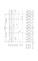
図4は、本発明における表示装置の動作を説明するタイミングチャートである。
図4において、P1(1)〜P1(m)は、第1行〜第m行にそれぞれ対応する走査信号P1を示している。P3(1)〜P3(m)は第1行〜第m行にそれぞれ対応する輝度制御信号P3を示している。第1行と第2行、第3行と第4行、第5行と第6行、第m−1行と第m行はそれぞれ同一の発光期間制御信号が入力されるため、P3(1)=P3(2)、P3(3)=P3(4)、P3(5)=P3(6)、・・・、P3(m−1)=P3(m)となっている。図の煩雑化を避けるために記載していないが、走査信号P2に関しては、図3に記載のタイミングと同様にして出力される。
FIG. 4 is a timing chart for explaining the operation of the display device according to the present invention.
In FIG. 4, P1 (1) to P1 (m) indicate scanning signals P1 corresponding to the first to mth rows, respectively. P3 (1) to P3 (m) indicate the luminance control signals P3 corresponding to the first to mth rows, respectively. Since the same light emission period control signal is input to the first row and the second row, the third row and the fourth row, the fifth row and the sixth row, the m−1th row and the mth row, respectively, P3 (1 ) = P3 (2), P3 (3) = P3 (4), P3 (5) = P3 (6),..., P3 (m−1) = P3 (m). Although not shown in order to avoid complication of the drawing, the scanning signal P2 is output in the same manner as the timing shown in FIG.
本発明では、インターレース方式により表示を行うため、1フレーム(図中の1frame)は奇数フィールド(図中のODDfield)と偶数フィールド(図中のEVEN field)からなる。 In the present invention, since display is performed by the interlace method, one frame (1 frame in the figure) is composed of an odd field (ODD field in the figure) and an even field (EVEN field in the figure).
奇数フィールドの間では、奇数行である第1行、第3行、第5行、・・・、第m−1行の走査信号P1(1)、P1(3)、P1(5)、・・・、P1(m−1)を順次、Highレベルにしている。すなわち奇数行の画素回路2のみについて電流データIdataを入力し、電流プログラミングしている。
Between the odd fields, the scan signals P1 (1), P1 (3), P1 (5) of the first, third, fifth,... ... P1 (m-1) is sequentially set to the high level. That is, the current data Idata is input only for the
偶数フィールドの間では、偶数行である第2行、第4行、第6行、・・・、第m行の走査信号P1(2)、P1(4)、P1(6)、・・・、P1(m)を順次、Highレベルにしている。すなわち偶数行の画素回路2のみについて電流データIdataを入力し、電流プログラミングしている。
Between even fields, the second row, fourth row, sixth row,..., M-th row scanning signals P1 (2), P1 (4), P1 (6),. , P1 (m) are sequentially set to the high level. That is, the current data Idata is input only for the
発光期間制御信号P3は、LowレベルでEL素子発光させる信号である。 The light emission period control signal P3 is a signal for causing the EL element to emit light at a low level.
同一のP3が入力される2つの行(例えば、第1行と第2行)は、いずれかのフィールドで電流プログラミングが行われた後、一定期間Lowレベル期間となり、この期間EL素子が発光する。 Two rows (for example, the first row and the second row) to which the same P3 is input become a low level period for a certain period after current programming is performed in any field, and the EL element emits light during this period. .
奇数フィールドにおいては奇数行が電流プログラミングされて、その直後から発光する。このとき偶数行のEL素子は、前のプログラミング時のデータを保存しているから、前の偶数フィールドと同じ輝度で2回目の発光が行われる。 In the odd field, the odd rows are current-programmed and light is emitted immediately after that. At this time, since the EL elements in the even-numbered rows store the data at the time of the previous programming, the second light emission is performed with the same luminance as the previous even-numbered field.
その次の偶数フィールドでは偶数行に電流プログラミングが行われて、偶数行のEL素子はその直後から発光する。奇数行のEL素子は先の奇数フィールドで与えられた電流プログラミングにしたがって発光する。 In the next even field, current programming is performed in the even-numbered row, and the EL elements in the even-numbered row emit light immediately after that. The odd row EL elements emit light according to the current programming given in the previous odd field.
このように、電流プログラミングを行うフィールド/行わないフィールドのいずれの場合にも発光期間を設けるので、1回の電流プログラミングに対してEL素子の発光を2回実施することができる。電流プログラミングを行わないフィールドでの発光期間は、その前のフィールドで画素回路にプログラミングされた電流で発光することとなる。つまり発光の周波数はフレーム周波数の2倍になり、フリッカを少なくすることができる.
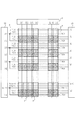
図5は、図4に示す表示装置の動作を実施する行制御回路3の一例である。
In this manner, since the light emission period is provided in both the field where current programming is performed and the field where current programming is not performed, light emission of the EL element can be performed twice for one current programming. In the light emission period in the field where current programming is not performed, light is emitted with the current programmed in the pixel circuit in the previous field. In other words, the emission frequency is twice the frame frequency, and flicker can be reduced.
FIG. 5 shows an example of the
図5において、行制御回路3は、フリップフロップ10からなるシフトレジスタ11を有しており、シフトレジスタ11の各出力はNOTゲート12、ANDゲート13からなるロジック回路14に入力され、バッファ15を通じてP1、P2、P3を出力する構成となっている。簡略化のため、第1行から第6行までの出力について図示している。
In FIG. 5, the
図6は図5の行制御回路の動作を説明するタイミングチャートである。SPはシフトレジスタ11に入力されるスタートパルス信号であり、CLKはシフトレジスタ11に入力されたSPを順次転送するクロック信号である。CLKの1周期は1走査期間とする。Q1〜Q4はシフトレジスタ11における各フリッププロップ10からの出力を示す。FIELDは奇数フィールドと偶数フィールドを判別するフィールド信号である。FIELDがHighレベル期間では奇数行の画素において電流プログラミングを行い、Lowレベル期間では偶数行の画素において電流プログラミングを行う。
FIG. 6 is a timing chart for explaining the operation of the row control circuit of FIG. SP is a start pulse signal input to the shift register 11, and CLK is a clock signal for sequentially transferring the SP input to the shift register 11. One cycle of CLK is one scanning period. Q1 to Q4 indicate outputs from the flip-
図5および図6によれば、各行のP1、P2は、シフトレジスタ11におけるその行に対応する段のフリップフロップ10と次段のフリップフロップ10の出力から生成され、P3は次段のフリップフロップ10の出力から生成される。
According to FIGS. 5 and 6, P1 and P2 of each row are generated from the outputs of the flip-
発光期間制御は、SPのHighレベル期間のパルス幅を変えてP3のLowレベルのパルス幅を変えることにより実施できる。 The light emission period can be controlled by changing the pulse width of the SP high level and changing the pulse width of the low level of P3.
図3に示したタイミングチャートによれば、P1およびP2が切り替わる時刻t1からある時間経った時刻t2にP3がLowレベルに切り替わる。これを実施するには、P3を出力するバッファの駆動能力をP1、P2のバッファより小さくすること、あるいはP3の出力のバッファを複数段にしたり容量を付加したりするなどして遅延回路を設けることなどが挙げられる。 According to the timing chart shown in FIG. 3, P3 switches to the Low level at time t2 after a certain time has elapsed from time t1 when P1 and P2 switch. In order to implement this, a delay circuit is provided by making the driving capacity of the buffer that outputs P3 smaller than that of the P1 and P2 buffers, or by adding a plurality of buffers or adding capacitors to the P3 output buffer. And so on.
本実施例においては、図5の構成による行制御回路を例示したが、これに限らず、図4の駆動方法を実施できる構成であればよい。 In the present embodiment, the row control circuit having the configuration of FIG. 5 is illustrated, but the present invention is not limited thereto, and any configuration that can implement the driving method of FIG.
以上のように、本実施例によれば、奇数フィールド/偶数フィールド交互に電流プログラミングを行いながらも各フィールド内に発光期間を設けているので、1フィールドの駆動周波数を60Hzにした場合には、電流プログラミングは30Hz(各行においてフレーム毎に1回)で行われるが、発光は60Hz(各行においてフィールド毎に1回)で行うことができる。すなわち、各画素において1回の電流プログラミングに対して発光回数は2回となる。こうして、発光/非発光の駆動周波数を電流プログラミングの2倍の駆動周波数にすることができるのでフリッカーの発生を抑制することが可能となる。 As described above, according to the present embodiment, since the light emission period is provided in each field while performing the current programming alternately in the odd field / even field, when the driving frequency of one field is set to 60 Hz, Current programming is done at 30 Hz (once per frame in each row), while light emission can be done at 60 Hz (once per field in each row). That is, the number of times of light emission is two times for each current programming in each pixel. In this manner, the light emission / non-light emission drive frequency can be set to a drive frequency twice that of the current programming, so that the occurrence of flicker can be suppressed.
図4において、1フレームの2回の発光期間(P3のパルス幅)は等しく設定されている。また各フィールド内でのタイミングも奇数フィールドと偶数フィールドで同じになっている。パルス幅、あるいはタイミングがフィールド間で大きく異なると、目に見える時間的に平均化された発光強度はフレーム周波数に等しくなってしまうから、フリッカーの抑制効果は生じない。 In FIG. 4, the two light emission periods of one frame (P3 pulse width) are set equal. The timing within each field is the same for odd and even fields. If the pulse width or the timing is greatly different between fields, the visible temporally averaged emission intensity becomes equal to the frame frequency, and thus the flicker suppressing effect does not occur.
本実施例における表示装置の全体構成は図1と同様であり、画素回路2およびその駆動方法も図2、図3と同様であるため、その説明および図を省略する。
The overall configuration of the display device in this embodiment is the same as that in FIG. 1, and the
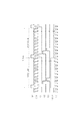
図7は、本発明における表示装置の他の駆動方法を説明するタイミングチャートである。
図7において、P1(1)〜P1(m)は、第1行〜第m行にそれぞれ対応する走査信号P1を示している。P3(1)〜P3(m)は第1行〜第m行にそれぞれ対応する輝度制御信号P3を示している。第1行と第2行、第3行と第4行、第5行と第6行、第m−1行と第m行はそれぞれ同一の発光期間制御信号が入力されるため、P3(1)=P3(2)、P3(3)=P3(4)、P3(5)=P3(6)、・・・、P3(m−1)=P3(m)となっている。図の煩雑化を避けるために記載していないが、走査信号P2に関しては、図3に記載のタイミングと同様にして出力される。
FIG. 7 is a timing chart for explaining another driving method of the display device according to the present invention.
In FIG. 7, P1 (1) to P1 (m) indicate scanning signals P1 corresponding to the first to mth rows, respectively. P3 (1) to P3 (m) indicate the luminance control signals P3 corresponding to the first to mth rows, respectively. Since the same light emission period control signal is input to the first row and the second row, the third row and the fourth row, the fifth row and the sixth row, the m−1th row and the mth row, respectively, P3 (1 ) = P3 (2), P3 (3) = P3 (4), P3 (5) = P3 (6),..., P3 (m−1) = P3 (m). Although not shown in order to avoid complication of the drawing, the scanning signal P2 is output in the same manner as the timing shown in FIG.
図4のタイミングチャートで説明した駆動方法と異なるのは、発光期間制御信号P3の出力波形である。
本実施例における発光期間制御信号P3は、同一のP3が入力される2つの行(例えば、第1行と第2行)のいずれかのP1がHighレベルの期間(電流プログラミング期間)である場合、必ずHighレベル期間(非発光期間)であり、かつ、電流プログラミング期間後、次回の電流プログラミングが行われるまでにLowレベル期間(発光期間)を複数回、設けている。
What is different from the driving method described in the timing chart of FIG. 4 is an output waveform of the light emission period control signal P3.
In the present embodiment, the light emission period control signal P3 is a period (current programming period) in which either P1 of two rows (for example, the first row and the second row) to which the same P3 is input is at a high level. The high level period (non-light emitting period) is always provided, and the low level period (light emitting period) is provided a plurality of times after the current programming period until the next current programming is performed.
実施例1と同様に、電流プログラミングを行うフィールド/行わないフィールドのいずれの場合にも発光期間を設け、電流プログラミングを行わないフィールドでの発光期間は、その前のフィールドでプログラミングされた電流で発光するのだが、本実施例では、さらに電流プログラミング1回に対してEL素子の発光/非発光を複数回繰り返すことができる。 As in the first embodiment, a light emission period is provided in each of the field where current programming is performed and the field where current programming is not performed, and the light emission period in the field where current programming is not performed is performed by the current programmed in the previous field. However, in this embodiment, the light emission / non-light emission of the EL element can be repeated a plurality of times for one current programming.
図8は、図7の制御信号が与えられて動作を行う行制御回路3の一例である。
FIG. 8 shows an example of the
図8において、行制御回路3は、フリップフロップ10からなるシフトレジスタ11A、シフトレジスタBを有している。シフトレジスタ11Aの各出力はNOTゲート12、ANDゲート13からなるロジック回路14Aに入力され、バッファ15を通じてP1、P2を出力する構成となっている。シフトレジスタ11Bの各出力は、バッファ15を通じてP3を出力する構成となっている。簡略化のため、第1行から第6行までの出力について図示している。
In FIG. 8, the
図9は図8の行制御回路の動作を説明するタイミングチャートである。SP1はシフトレジスタ11Aに入力されるスタートパルス信号1であり、Highレベルの信号のパルス幅は1走査期間とする。SP2はシフトレジスタ11Bに入力されるスタートパルス信号2である。CLKは、シフトレジスタ11Aおよびシフトレジスタ11Bに共通に入力され、またシフトレジスタ11Aに入力されたSP1、およびシフトレジスタ11Bに入力されたSP2を順次転送するクロック信号である。CLKの1周期は1走査期間とする。Q1A〜Q3Aはシフトレジスタ11Aにおける各フリッププロップ10からの出力を示す。Q1B〜Q3Bはシフトレジスタ11Bにおける各フリッププロップ10からの出力を示す。FIELDは奇数フィールドと偶数フィールドを判別するフィールド信号である。FIELDがHighレベル期間では奇数行の画素において電流プログラミングを行い、Lowレベル期間では偶数行の画素において電流プログラミングを行う。
FIG. 9 is a timing chart for explaining the operation of the row control circuit of FIG. SP1 is a
SP1がHighレベルの期間では、SP2もHighレベルにする。こうすることでP1がHighレベルの期間(電流プログラミング期間)は、必ずP3がHighレベル期間(非発光期間)になる。 During the period when SP1 is at the high level, SP2 is also set at the high level. By doing so, P3 is always in a high level period (non-light emitting period) during a period in which P1 is at high level (current programming period).
発光期間制御は、SP2のLowレベル期間のパルス幅を変えてP3のLowレベルのパルス幅を変えたり、Lowレベル期間の回数を変えたりすることにより実施できる。しかし、いずれの場合もパルスの期間と間隔はどこも一様であることが好ましい。1つのパルスだけを長くすると、目に感じる発光強度の時間変化はフレーム周波数と変わらなくなってしまう。 The light emission period control can be performed by changing the pulse width of the low level period of SP2 to change the pulse width of the low level of P3 or changing the number of times of the low level period. However, in any case, it is preferable that the pulse period and interval are uniform everywhere. If only one pulse is lengthened, the temporal change in the light emission intensity perceived by the eye does not change from the frame frequency.
図3に示したタイミングチャートによれば、P1およびP2が切り替わる時刻t1からある時間経った時刻t2にP3がLowレベルに切り替わる。これを実施するには、実施例1に記載したように、P3を出力するバッファの駆動能力をP1、P2のバッファより小さくすること、あるいはP3の出力のバッファを複数段にしたり容量を付加したりするなどして遅延回路を設けることなどが挙げられる。 According to the timing chart shown in FIG. 3, P3 switches to the Low level at time t2 after a certain time has elapsed from time t1 when P1 and P2 switch. In order to implement this, as described in the first embodiment, the drive capacity of the buffer that outputs P3 is made smaller than that of the P1 and P2 buffers, or the output buffer of P3 is made into a plurality of stages or a capacity is added. For example, a delay circuit may be provided.
本実施例では、シフトレジスタ11AとシフトレジスタBに共通のCLKを入力したが、各シフトレジスタに別々のクロック信号を入力してもよい。 In this embodiment, the common CLK is input to the shift register 11A and the shift register B, but separate clock signals may be input to the shift registers.
また、図10は、本実施例における表示装置の他の全体構成を示している。
図10に示す表示装置では、行制御回路3A、行制御回路3Bを有している。図8におけるa部を行制御回路3A、b部を行制御回路3Bのように分離して配置しても良い。
FIG. 10 shows another overall configuration of the display device according to this embodiment.
The display device illustrated in FIG. 10 includes a
本実施例においては、図8の構成による行制御回路を例示したが、これに限らず、図7の駆動方法を実施できる構成であればよい。 In the present embodiment, the row control circuit having the configuration of FIG. 8 is illustrated, but the present invention is not limited to this, and any configuration that can implement the driving method of FIG.
以上のように、本実施例によれば、奇数フィールド/偶数フィールド交互に電流プログラミングを行いながらも各フィールド内に複数の発光期間を設けている。よって、1フィールドの駆動周波数を60Hzにした場合には、電流プログラミングは30Hz(各行においてフレーム毎に1回)で行われ、発光は120Hz(各行においてフィールド毎に2回発光するとき)あるいはさらに回数を増やせばそれ以上の周波数で行うことができる。こうして、発光/非発光の駆動周波数を高くすることができるのでフリッカーの発生を抑制することが可能となる。 As described above, according to the present embodiment, a plurality of light emission periods are provided in each field while performing current programming alternately in odd and even fields. Therefore, when the driving frequency of one field is set to 60 Hz, current programming is performed at 30 Hz (once per frame in each row), and light emission is performed at 120 Hz (when light is emitted twice per field in each row) or more times If it is increased, it can be performed at a higher frequency. In this way, since the driving frequency of light emission / non-light emission can be increased, the occurrence of flicker can be suppressed.
図11は、本実施例による表示装置の全体構成を示す。
図11において、画像表示部には、RGB原色数のEL素子と、このEL素子に入力される電流を制御するためのTFTから構成される画素回路2とが画素1を構成してm行×n列の2次元状に配列されている。ここでmは偶数、nは自然数とする。表示領域の周辺には行制御回路3、および列制御回路4を備えている。行制御回路3Cの各出力端子からは走査信号P1(1)〜P1(m)、P2(1)〜P2(m)と発光期間制御信号P3(1)〜P3(m)が出力される。走査信号は走査線5を介して各行の画素回路2に入力される。発光期間制御信号は発光期間制御線6を介して各行の画素回路2に入力される。図1とは異なり、発光期間制御線6は全行独立に画素回路2に入力される。列制御回路4には映像信号が入力され、各出力端子から電流データIdataが出力される。電流データIdataはデータ線7を介して各列の画素回路に入力される。
FIG. 11 shows the overall configuration of the display device according to this embodiment.
In FIG. 11, in the image display unit, an EL element having the number of RGB primary colors and a
本実施例における画素回路2およびその駆動方法は図2、図3と同様であるため、その説明および図を省略する。
Since the
図12は、本発明における表示装置の駆動方法を説明するタイミングチャートである。
図12において、P1(1)〜P1(m)は、第1行〜第m行にそれぞれ対応する走査信号P1を示している。P3(1)〜P3(m)は第1行〜第m行にそれぞれ対応する輝度制御信号P3を示している。図の煩雑化を避けるために記載していないが、走査信号P2に関しては、図3に記載のタイミングと同様にして出力される。
FIG. 12 is a timing chart illustrating a method for driving a display device according to the present invention.
In FIG. 12, P1 (1) to P1 (m) indicate scanning signals P1 corresponding to the first to mth rows, respectively. P3 (1) to P3 (m) indicate the luminance control signals P3 corresponding to the first to mth rows, respectively. Although not shown in order to avoid complication of the drawing, the scanning signal P2 is output in the same manner as the timing shown in FIG.
図4、図7のタイミングチャートで説明した駆動方法と異なるのは、発光期間制御信号P3の出力波形である。 What is different from the driving method described in the timing charts of FIGS. 4 and 7 is an output waveform of the light emission period control signal P3.
本実施例における発光期間制御信号P3は、全行において1周期を1走査期間としてHigh/Lowを繰り返す連続信号である。ただし、P1がHighレベルの期間(電流プログラミング期間)では、その行のP3は必ずHighレベル期間(非発光期間)とする。 The light emission period control signal P3 in the present embodiment is a continuous signal that repeats High / Low with one cycle as one scanning period in all rows. However, in a period in which P1 is at a high level (current programming period), P3 in the row is always a high level period (non-light emitting period).
実施例1、実施例2と同様に、電流プログラミングを行うフィールド/行わないフィールドのいずれの場合にも発光期間を設け、電流プログラミングを行わないフィールドでの発光期間は、その前のフィールドでプログラミングされた電流で発光する。また、実施例2と同様に、電流プログラミング1回に対してEL素子の発光/非発光を複数回繰り返すことができる。 As in the first and second embodiments, a light emission period is provided in each of the fields for which current programming is performed and the fields for which current programming is not performed, and the light emission period in the field where current programming is not performed is programmed in the previous field. Emits light with a high current. Similarly to the second embodiment, light emission / non-light emission of the EL element can be repeated a plurality of times for one current programming.
図13は、図11に示す表示装置の動作を実施する行制御回路3Cの一例である。
図13において、行制御回路3Cは、フリップフロップ10からなるシフトレジスタ11Cを有しており、シフトレジスタ11Cの各出力はNOTゲート12、ANDゲート13、ORゲート16からなるロジック回路14Bに入力され、バッファ15を通じてP1、P2、P3を出力する構成となっている。簡略化のため、第1行から第6行までの出力について図示している。
FIG. 13 is an example of a
In FIG. 13, the
図14は図13の行制御回路の動作を説明するタイミングチャートである。SPはシフトレジスタ11Cに入力されるスタートパルス信号であり、Highレベルの信号のパルス幅は1走査期間とする。CLKはシフトレジスタ11Cに入力されたSPを順次転送するクロック信号である。CLKの1周期は1走査期間とする。Q1〜Q3はシフトレジスタ11Cにおける各フリッププロップ10からの出力を示す。FIELDは奇数フィールドと偶数フィールドを判別するフィールド信号である。FIELDがHighレベル期間では奇数行の画素において電流プログラミングを行い、Lowレベル期間では偶数行の画素において電流プログラミングを行う。
FIG. 14 is a timing chart for explaining the operation of the row control circuit of FIG. SP is a start pulse signal input to the shift register 11C, and the pulse width of the high level signal is one scanning period. CLK is a clock signal for sequentially transferring SPs input to the shift register 11C. One cycle of CLK is one scanning period. Q1 to Q3 indicate outputs from the flip-
LCはP3のHighレベル期間/Lowレベル期間を規定するP3制御信号であり、1周期を1走査期間としてHighレベル期間/Lowレベル期間を繰り返す。 LC is a P3 control signal that defines the high level period / low level period of P3, and repeats the high level period / low level period with one period as one scanning period.
P1がHighレベルの期間(電流プログラミング期間)は、P3はLCに関係なく必ずHighレベル期間(非発光期間)になる。 During a period when P1 is at a high level (current programming period), P3 always becomes a high level period (non-light emitting period) regardless of LC.
発光期間制御は、LCのデューディー比を変えてP3のLowレベルのパルス幅を変えることにより実施できる。 The light emission period control can be performed by changing the pulse width of the low level of P3 by changing the duty ratio of the LC.
また本実施例において、LCは最良の形態として1周期を1走査期間としてHighレベル期間/Lowレベル期間を繰り返す連続信号としているが、必ずしも1周期を1走査期間としなくてもよく、周期的に繰り返す連続信号であればよい。 In the present embodiment, as the best mode, the LC is a continuous signal that repeats the High level period / Low level period with one period as one scanning period. However, one period does not necessarily have to be one scanning period. Any continuous signal may be used.
図3に示したタイミングチャートによれば、P1およびP2が切り替わる時刻t1からある時間経った時刻t2にP3がLowレベルに切り替わる。これを実施するには、実施例1、および実施例2に記載したように、P3を出力するバッファの駆動能力をP1、P2のバッファより小さくすること、あるいはP3の出力のバッファを複数段にしたり容量を付加したりするなどして遅延回路を設けることなどが挙げられる。 According to the timing chart shown in FIG. 3, P3 switches to the Low level at time t2 after a certain time has elapsed from time t1 when P1 and P2 switch. In order to implement this, as described in the first and second embodiments, the drive capacity of the buffer that outputs P3 is made smaller than that of the P1 and P2 buffers, or the output buffer of P3 is formed in a plurality of stages. For example, a delay circuit may be provided by adding a capacitor.
本実施例においては、図13の構成による行制御回路を例示したが、これに限らず、図12の駆動方法を実施できる構成であればよい。 In the present embodiment, the row control circuit having the configuration of FIG. 13 is exemplified, but the present invention is not limited to this, and any configuration that can implement the driving method of FIG.
以上のように、本実施例によれば、奇数フィールド/偶数フィールド交互に電流プログラミングを行いながらも、(電流プログラミング期間以外において)1走査期間毎に発光期間を設けている。よって、1フィールドの駆動周波数を60Hzにした場合には、電流プログラミングは30Hz(各行においてフレーム毎に1回)で行われるが、発光は60Hz以上で行うことができる。例えば、NTSC規格と同様に1フレーム期間が525走査期間あったとすると、1フレーム期間での発光回数は524回(電流プログラミング時の1走査期間を除くため)となる。こうして、発光/非発光の駆動周波数を高くすることができるのでフリッカーの発生を抑制することが可能となる。 As described above, according to the present embodiment, the light emission period is provided for each scanning period (other than the current programming period) while performing the current programming alternately in the odd field / even field. Therefore, when the driving frequency of one field is set to 60 Hz, current programming is performed at 30 Hz (once per frame in each row), but light emission can be performed at 60 Hz or more. For example, if one frame period is 525 scanning periods as in the NTSC standard, the number of times of light emission in one frame period is 524 times (since one scanning period during current programming is excluded). In this way, since the driving frequency of light emission / non-light emission can be increased, the occurrence of flicker can be suppressed.
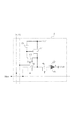
本実施例は、上述した各実施例を電子機器に用いた例である。
図15は、本実施例のデジタルスチルカメラシステムの一例のブロック図である。図中、50はデジタルスチルカメラシステム、51は撮影部、52は映像信号処理回路、53は表示パネル、54はメモリ、55はCPU、56は操作部を示す。
The present embodiment is an example in which each of the above-described embodiments is used in an electronic device.
FIG. 15 is a block diagram of an example of the digital still camera system of the present embodiment. In the figure, 50 is a digital still camera system, 51 is a photographing unit, 52 is a video signal processing circuit, 53 is a display panel, 54 is a memory, 55 is a CPU, and 56 is an operation unit.
図15において、撮像部51で撮影した映像または、メモリ54に記録された映像を、映像信号処理回路52で信号処理し、表示パネル53で見ることができる。CPU55では、操作部56からの入力によって、撮影部51、メモリ54、映像信号処理回路52などを制御して、状況に適した撮影、記録、再生、表示を行う。また、表示パネル53は、この他にも各種電子機器の表示部として利用できる。
In FIG. 15, an image captured by the
本発明は、電流プログラミング装置、アクティブマトリクス型表示装置、およびこれらの電流供給方法に係わり、特に電流駆動型表示素子に用いたアクティブマトリクス型表示装置に適用される。この表示装置を用いて、例えば情報表示装置を構成できる。この情報表示装置は、例えば携帯電話、携帯コンピュータ、スチルカメラもしくはビデオカメラのいずれかの形態をとる。もしくは、それらの各機能の複数を実現する装置である。情報表示装置は、情報入力部を備えている。例えば、携帯電話の場合には情報入力部は、アンテナを含んで構成される。PDAや携帯PCの場合には、情報入力部は、ネットワークに対するインターフェース部を含んで構成される。スチルカメラやムービーカメラの場合には、情報入力部はCCDやCMOSなどによるセンサ部を含んで構成される。 The present invention relates to a current programming device, an active matrix display device, and a method for supplying these currents, and is particularly applied to an active matrix display device used for a current driven display element. For example, an information display device can be configured using this display device. This information display device takes the form of, for example, a mobile phone, a mobile computer, a still camera, or a video camera. Alternatively, it is a device that realizes a plurality of these functions. The information display device includes an information input unit. For example, in the case of a mobile phone, the information input unit includes an antenna. In the case of a PDA or a portable PC, the information input unit includes an interface unit for a network. In the case of a still camera or a movie camera, the information input unit includes a sensor unit such as a CCD or CMOS.
1 画素
2 画素回路
3、3A、3B、3C 行制御回路
4 列制御回路
5 走査線
6 発光期間制御線
7 データ線
10 フリップフロップ
11、11A、11B、11C シフトレジスタ
12 NOTゲート
13 ANDゲート
14、14A、14B ロジック回路
15 バッファ
16 ORゲート
50 デジタルスチルカメラシステム
51 撮影部
52 映像信号処理回路
53 表示パネル
54 メモリ
55 CPU
56 操作部
1
56 Operation unit
Claims (10)
電流の値が設定され、設定された電流を前記表示素子に供給する画素回路と、
前記表示素子と前記画素回路の組が行方向および列方向にマトリクス状に複数配置された画像表示部と、
前記画像表示部の行毎に設けられた走査線と、
前記画像表示部の行毎に設けられた発光期間制御線と、
前記画像表示部の行数に応じて配置され、前記画素回路が前記表示素子に供給する電流を設定する期間を制御する走査信号を前記走査線に出力し、かつ前記画素回路が前記表示素子に電流を供給する期間を制御する発光期間制御信号を前記発光期間制御線に出力する行制御回路と、
前記画像表示部の列毎に設けられたデータ線と、
前記画像表示部の列数に応じて配置され、前記画素回路が前記表示素子に供給する電流に応じたデータ信号を前記データ線に出力する列制御回路と、
を有する表示装置であって、
前記行制御回路が前記画像表示部の奇数行の前記走査線に前記走査信号を出力し、前記列制御回路が前記データ信号を前記データ線に出力して、前記画像表示部の奇数行の表示素子に供給する電流を当該表示素子の前記画素回路に設定する第1の動作と、
前記行制御回路が前記画像表示部の偶数行の前記走査線に前記走査信号を出力し、前記列制御回路が前記データ信号を前記データ線に出力して、前記画像表示部の偶数行の表示素子に供給する電流を当該表示素子の前記画素回路に設定する第2の動作とを交互に繰り返して行い、
前記第1と第2の動作の繰り返しの周期に同期して、前記繰り返し周期内に前記第1または第2の動作により電流が設定される回数の2倍以上の回数、前記行制御回路が前記画像表示部の奇数行と偶数行の前記発光期間制御線に前記発光期間制御信号を出力し、前記表示素子に、当該表示素子の前記画素回路内に設定された電流を一定期間供給することを特徴とする表示装置。 A display element whose emission luminance is controlled according to the current;
A pixel circuit in which a current value is set and the set current is supplied to the display element;
An image display unit in which a plurality of sets of the display element and the pixel circuit are arranged in a matrix in a row direction and a column direction;
A scanning line provided for each row of the image display unit;
A light emission period control line provided for each row of the image display unit;
A scanning signal that is arranged according to the number of rows of the image display unit and that controls a period for setting a current that the pixel circuit supplies to the display element is output to the scanning line, and the pixel circuit is applied to the display element. A row control circuit for outputting a light emission period control signal for controlling a period for supplying a current to the light emission period control line;
A data line provided for each column of the image display unit;
A column control circuit that is arranged according to the number of columns of the image display unit and outputs a data signal to the data line according to a current supplied from the pixel circuit to the display element;
A display device comprising:
The row control circuit outputs the scanning signal to the scanning lines in odd rows of the image display unit, and the column control circuit outputs the data signal to the data lines, thereby displaying odd rows in the image display unit. A first operation of setting a current supplied to the element to the pixel circuit of the display element;
The row control circuit outputs the scanning signal to the even-numbered scanning lines of the image display unit, and the column control circuit outputs the data signal to the data line to display even-numbered rows of the image display unit. A second operation of setting a current supplied to the element in the pixel circuit of the display element is alternately repeated,
Synchronously with the repetition cycle of the first and second operations, the row control circuit performs the number of times more than twice the number of times the current is set by the first or second operation within the repetition cycle. The light emission period control signal is output to the light emission period control lines of the odd-numbered and even-numbered lines of the image display unit, and the current set in the pixel circuit of the display element is supplied to the display element for a certain period. Characteristic display device.
An electronic device equipped with the display device according to claim 1.
Priority Applications (4)
| Application Number | Priority Date | Filing Date | Title |
|---|---|---|---|
| JP2006098011A JP5058505B2 (en) | 2006-03-31 | 2006-03-31 | Display device |
| CN2007800113794A CN101410884B (en) | 2006-03-31 | 2007-03-30 | Display device |
| PCT/JP2007/057708 WO2007116950A1 (en) | 2006-03-31 | 2007-03-30 | Display device |
| US11/917,068 US7911425B2 (en) | 2006-03-31 | 2007-03-30 | Display device |
Applications Claiming Priority (1)
| Application Number | Priority Date | Filing Date | Title |
|---|---|---|---|
| JP2006098011A JP5058505B2 (en) | 2006-03-31 | 2006-03-31 | Display device |
Publications (3)
| Publication Number | Publication Date |
|---|---|
| JP2007271973A true JP2007271973A (en) | 2007-10-18 |
| JP2007271973A5 JP2007271973A5 (en) | 2009-05-07 |
| JP5058505B2 JP5058505B2 (en) | 2012-10-24 |
Family
ID=38370979
Family Applications (1)
| Application Number | Title | Priority Date | Filing Date |
|---|---|---|---|
| JP2006098011A Expired - Fee Related JP5058505B2 (en) | 2006-03-31 | 2006-03-31 | Display device |
Country Status (4)
| Country | Link |
|---|---|
| US (1) | US7911425B2 (en) |
| JP (1) | JP5058505B2 (en) |
| CN (1) | CN101410884B (en) |
| WO (1) | WO2007116950A1 (en) |
Cited By (2)
| Publication number | Priority date | Publication date | Assignee | Title |
|---|---|---|---|---|
| JP2009025797A (en) * | 2007-06-19 | 2009-02-05 | Canon Inc | Display apparatus and electronic device using the same |
| JP2010175586A (en) * | 2009-01-27 | 2010-08-12 | Seiko Epson Corp | Light emitting device and electronic equipment |
Families Citing this family (19)
| Publication number | Priority date | Publication date | Assignee | Title |
|---|---|---|---|---|
| JP2009014836A (en) * | 2007-07-02 | 2009-01-22 | Canon Inc | Active matrix type display and driving method therefor |
| KR101091616B1 (en) * | 2007-08-21 | 2011-12-08 | 캐논 가부시끼가이샤 | Display apparatus and drive method thereof |
| JP2009080272A (en) * | 2007-09-26 | 2009-04-16 | Canon Inc | Active matrix type display device |
| JP2009109641A (en) * | 2007-10-29 | 2009-05-21 | Canon Inc | Driving circuit and active matrix type display device |
| JP4816686B2 (en) * | 2008-06-06 | 2011-11-16 | ソニー株式会社 | Scan driver circuit |
| JP2010008987A (en) * | 2008-06-30 | 2010-01-14 | Canon Inc | Drive circuit |
| JP2010122355A (en) * | 2008-11-18 | 2010-06-03 | Canon Inc | Display apparatus and camera |
| JP5284198B2 (en) * | 2009-06-30 | 2013-09-11 | キヤノン株式会社 | Display device and driving method thereof |
| JP2011013415A (en) * | 2009-07-01 | 2011-01-20 | Canon Inc | Active matrix type display apparatus |
| JP2011028135A (en) * | 2009-07-29 | 2011-02-10 | Canon Inc | Display device and driving method of the same |
| KR101703875B1 (en) * | 2010-08-20 | 2017-02-07 | 엘지디스플레이 주식회사 | LCD and method of driving the same |
| US20120081347A1 (en) * | 2010-09-30 | 2012-04-05 | Apple Inc. | Low power inversion scheme with minimized number of output transitions |
| KR20120044507A (en) * | 2010-10-28 | 2012-05-08 | 삼성모바일디스플레이주식회사 | Organic light emitting display device and driving method thereof |
| JP6124573B2 (en) | 2011-12-20 | 2017-05-10 | キヤノン株式会社 | Display device |
| CN103116429A (en) * | 2013-01-31 | 2013-05-22 | 敦泰科技有限公司 | Scan method, device, controller and electronic device orienting towards in-cell technology |
| JP6478518B2 (en) | 2014-08-11 | 2019-03-06 | キヤノン株式会社 | Light emitting device and image forming apparatus |
| KR102568899B1 (en) * | 2016-11-04 | 2023-08-21 | 삼성전자주식회사 | LED display device, and method for operating the same |
| US11749157B2 (en) | 2022-01-25 | 2023-09-05 | Wuhan China Star Optoelectronics Semiconductor Display Technology Co., Ltd. | Display panel and display device |
| CN114420029B (en) * | 2022-01-25 | 2023-08-22 | 武汉华星光电半导体显示技术有限公司 | Display panel and display device |
Citations (2)
| Publication number | Priority date | Publication date | Assignee | Title |
|---|---|---|---|---|
| JP2004029755A (en) * | 2002-04-26 | 2004-01-29 | Toshiba Matsushita Display Technology Co Ltd | Electroluminescence display device |
| JP2007017936A (en) * | 2005-06-09 | 2007-01-25 | Seiko Epson Corp | Light-emitting device, driving method thereof, and electronic apparatus |
Family Cites Families (12)
| Publication number | Priority date | Publication date | Assignee | Title |
|---|---|---|---|---|
| US7227517B2 (en) * | 2001-08-23 | 2007-06-05 | Seiko Epson Corporation | Electronic device driving method, electronic device, semiconductor integrated circuit, and electronic apparatus |
| US20050180083A1 (en) * | 2002-04-26 | 2005-08-18 | Toshiba Matsushita Display Technology Co., Ltd. | Drive circuit for el display panel |
| JP2004191752A (en) * | 2002-12-12 | 2004-07-08 | Seiko Epson Corp | Electrooptical device, driving method for electrooptical device, and electronic equipment |
| JP3950845B2 (en) | 2003-03-07 | 2007-08-01 | キヤノン株式会社 | Driving circuit and evaluation method thereof |
| US7812812B2 (en) | 2003-03-25 | 2010-10-12 | Canon Kabushiki Kaisha | Driving method of display apparatus |
| JP4838498B2 (en) | 2003-05-21 | 2011-12-14 | キヤノン株式会社 | Display device |
| JP4054794B2 (en) | 2003-12-04 | 2008-03-05 | キヤノン株式会社 | DRIVE DEVICE, DISPLAY DEVICE, AND RECORDING DEVICE |
| US7608861B2 (en) | 2004-06-24 | 2009-10-27 | Canon Kabushiki Kaisha | Active matrix type display having two transistors of opposite conductivity acting as a single switch for the driving transistor of a display element |
| JP4438066B2 (en) | 2004-11-26 | 2010-03-24 | キヤノン株式会社 | Active matrix display device and current programming method thereof |
| JP4438067B2 (en) | 2004-11-26 | 2010-03-24 | キヤノン株式会社 | Active matrix display device and current programming method thereof |
| JP4438069B2 (en) | 2004-12-03 | 2010-03-24 | キヤノン株式会社 | Current programming device, active matrix display device, and current programming method thereof |
| US7872617B2 (en) | 2005-10-12 | 2011-01-18 | Canon Kabushiki Kaisha | Display apparatus and method for driving the same |
-
2006
- 2006-03-31 JP JP2006098011A patent/JP5058505B2/en not_active Expired - Fee Related
-
2007
- 2007-03-30 WO PCT/JP2007/057708 patent/WO2007116950A1/en active Application Filing
- 2007-03-30 US US11/917,068 patent/US7911425B2/en not_active Expired - Fee Related
- 2007-03-30 CN CN2007800113794A patent/CN101410884B/en not_active Expired - Fee Related
Patent Citations (2)
| Publication number | Priority date | Publication date | Assignee | Title |
|---|---|---|---|---|
| JP2004029755A (en) * | 2002-04-26 | 2004-01-29 | Toshiba Matsushita Display Technology Co Ltd | Electroluminescence display device |
| JP2007017936A (en) * | 2005-06-09 | 2007-01-25 | Seiko Epson Corp | Light-emitting device, driving method thereof, and electronic apparatus |
Cited By (2)
| Publication number | Priority date | Publication date | Assignee | Title |
|---|---|---|---|---|
| JP2009025797A (en) * | 2007-06-19 | 2009-02-05 | Canon Inc | Display apparatus and electronic device using the same |
| JP2010175586A (en) * | 2009-01-27 | 2010-08-12 | Seiko Epson Corp | Light emitting device and electronic equipment |
Also Published As
| Publication number | Publication date |
|---|---|
| US7911425B2 (en) | 2011-03-22 |
| WO2007116950A1 (en) | 2007-10-18 |
| US20090231239A1 (en) | 2009-09-17 |
| JP5058505B2 (en) | 2012-10-24 |
| CN101410884B (en) | 2011-12-14 |
| CN101410884A (en) | 2009-04-15 |
Similar Documents
| Publication | Publication Date | Title |
|---|---|---|
| JP5058505B2 (en) | Display device | |
| JP5495510B2 (en) | Display device and electronic apparatus using the same | |
| JP4284558B2 (en) | Display drive device, display device, and drive control method thereof | |
| JP4552844B2 (en) | LIGHT EMITTING DEVICE, ITS DRIVE METHOD, AND ELECTRONIC DEVICE | |
| JP2011028135A (en) | Display device and driving method of the same | |
| JP2004252104A (en) | Electro-optic device, method for driving electro-optic device, and electronic equipment | |
| JP2006119179A (en) | Electro-optic device, driving method therefor, and electronic equipment | |
| JP2006047973A (en) | Organic el display device and demultiplexer | |
| CN110706653A (en) | Drive circuit, display panel, drive method and display device | |
| JP4304585B2 (en) | CURRENT GENERATION SUPPLY CIRCUIT, CONTROL METHOD THEREOF, AND DISPLAY DEVICE PROVIDED WITH THE CURRENT GENERATION SUPPLY CIRCUIT | |
| JP2008039799A (en) | Display device and drive control method thereof | |
| CN113692612A (en) | Display device, method of driving display device, and electronic apparatus | |
| JP2007133351A (en) | Display unit, active matrix device, and driving method thereof | |
| CN112785969A (en) | Electroluminescent display panel with light emitting drive circuit | |
| JP2003255880A (en) | Semiconductor ic circuit and its driving method | |
| JP2011128442A (en) | Display panel, display device and electronic equipment | |
| JP4337327B2 (en) | Display and electronic equipment | |
| KR100581808B1 (en) | Light emitting display by using demultiplexer | |
| KR20210043047A (en) | Display device | |
| KR100882674B1 (en) | Organic elcetroluminescence display and driving method thereof | |
| JP5207685B2 (en) | Display device and driving method thereof | |
| JP2010156839A (en) | Display device and driving method | |
| JP4617284B2 (en) | Display device | |
| JP4941426B2 (en) | Display device | |
| KR100629584B1 (en) | Light emitting display and driving method thereof |
Legal Events
| Date | Code | Title | Description |
|---|---|---|---|
| A521 | Request for written amendment filed |
Free format text: JAPANESE INTERMEDIATE CODE: A523 Effective date: 20090324 |
|
| A621 | Written request for application examination |
Free format text: JAPANESE INTERMEDIATE CODE: A621 Effective date: 20090324 |
|
| RD04 | Notification of resignation of power of attorney |
Free format text: JAPANESE INTERMEDIATE CODE: A7424 Effective date: 20100201 |
|
| RD01 | Notification of change of attorney |
Free format text: JAPANESE INTERMEDIATE CODE: A7421 Effective date: 20100630 |
|
| A131 | Notification of reasons for refusal |
Free format text: JAPANESE INTERMEDIATE CODE: A131 Effective date: 20111108 |
|
| A521 | Request for written amendment filed |
Free format text: JAPANESE INTERMEDIATE CODE: A523 Effective date: 20120105 |
|
| A131 | Notification of reasons for refusal |
Free format text: JAPANESE INTERMEDIATE CODE: A131 Effective date: 20120508 |
|
| A521 | Request for written amendment filed |
Free format text: JAPANESE INTERMEDIATE CODE: A523 Effective date: 20120705 |
|
| TRDD | Decision of grant or rejection written | ||
| A01 | Written decision to grant a patent or to grant a registration (utility model) |
Free format text: JAPANESE INTERMEDIATE CODE: A01 Effective date: 20120731 |
|
| A01 | Written decision to grant a patent or to grant a registration (utility model) |
Free format text: JAPANESE INTERMEDIATE CODE: A01 |
|
| A61 | First payment of annual fees (during grant procedure) |
Free format text: JAPANESE INTERMEDIATE CODE: A61 Effective date: 20120801 |
|
| FPAY | Renewal fee payment (event date is renewal date of database) |
Free format text: PAYMENT UNTIL: 20150810 Year of fee payment: 3 |
|
| FPAY | Renewal fee payment (event date is renewal date of database) |
Free format text: PAYMENT UNTIL: 20150810 Year of fee payment: 3 |
|
| LAPS | Cancellation because of no payment of annual fees |