JP2007267392A - Error detection in physical interface for point to point communications between integrated circuits - Google Patents
Error detection in physical interface for point to point communications between integrated circuits Download PDFInfo
- Publication number
- JP2007267392A JP2007267392A JP2007101084A JP2007101084A JP2007267392A JP 2007267392 A JP2007267392 A JP 2007267392A JP 2007101084 A JP2007101084 A JP 2007101084A JP 2007101084 A JP2007101084 A JP 2007101084A JP 2007267392 A JP2007267392 A JP 2007267392A
- Authority
- JP
- Japan
- Prior art keywords
- bits
- error
- error detection
- physical interface
- data bits
- Prior art date
- Legal status (The legal status is an assumption and is not a legal conclusion. Google has not performed a legal analysis and makes no representation as to the accuracy of the status listed.)
- Pending
Links
Images


Classifications
-
- H—ELECTRICITY
- H04—ELECTRIC COMMUNICATION TECHNIQUE
- H04L—TRANSMISSION OF DIGITAL INFORMATION, e.g. TELEGRAPHIC COMMUNICATION
- H04L1/00—Arrangements for detecting or preventing errors in the information received
-
- H—ELECTRICITY
- H04—ELECTRIC COMMUNICATION TECHNIQUE
- H04L—TRANSMISSION OF DIGITAL INFORMATION, e.g. TELEGRAPHIC COMMUNICATION
- H04L1/00—Arrangements for detecting or preventing errors in the information received
- H04L1/004—Arrangements for detecting or preventing errors in the information received by using forward error control
- H04L1/0045—Arrangements at the receiver end
-
- H—ELECTRICITY
- H04—ELECTRIC COMMUNICATION TECHNIQUE
- H04L—TRANSMISSION OF DIGITAL INFORMATION, e.g. TELEGRAPHIC COMMUNICATION
- H04L1/00—Arrangements for detecting or preventing errors in the information received
- H04L1/004—Arrangements for detecting or preventing errors in the information received by using forward error control
- H04L1/0056—Systems characterized by the type of code used
- H04L1/0061—Error detection codes
-
- H—ELECTRICITY
- H04—ELECTRIC COMMUNICATION TECHNIQUE
- H04L—TRANSMISSION OF DIGITAL INFORMATION, e.g. TELEGRAPHIC COMMUNICATION
- H04L25/00—Baseband systems
- H04L25/38—Synchronous or start-stop systems, e.g. for Baudot code
- H04L25/40—Transmitting circuits; Receiving circuits
- H04L25/49—Transmitting circuits; Receiving circuits using code conversion at the transmitter; using predistortion; using insertion of idle bits for obtaining a desired frequency spectrum; using three or more amplitude levels ; Baseband coding techniques specific to data transmission systems
- H04L25/4906—Transmitting circuits; Receiving circuits using code conversion at the transmitter; using predistortion; using insertion of idle bits for obtaining a desired frequency spectrum; using three or more amplitude levels ; Baseband coding techniques specific to data transmission systems using binary codes
- H04L25/4908—Transmitting circuits; Receiving circuits using code conversion at the transmitter; using predistortion; using insertion of idle bits for obtaining a desired frequency spectrum; using three or more amplitude levels ; Baseband coding techniques specific to data transmission systems using binary codes using mBnB codes
-
- H—ELECTRICITY
- H04—ELECTRIC COMMUNICATION TECHNIQUE
- H04L—TRANSMISSION OF DIGITAL INFORMATION, e.g. TELEGRAPHIC COMMUNICATION
- H04L69/00—Network arrangements, protocols or services independent of the application payload and not provided for in the other groups of this subclass
- H04L69/30—Definitions, standards or architectural aspects of layered protocol stacks
- H04L69/32—Architecture of open systems interconnection [OSI] 7-layer type protocol stacks, e.g. the interfaces between the data link level and the physical level
-
- H—ELECTRICITY
- H04—ELECTRIC COMMUNICATION TECHNIQUE
- H04L—TRANSMISSION OF DIGITAL INFORMATION, e.g. TELEGRAPHIC COMMUNICATION
- H04L9/00—Cryptographic mechanisms or cryptographic arrangements for secret or secure communications; Network security protocols
- H04L9/40—Network security protocols
-
- H—ELECTRICITY
- H04—ELECTRIC COMMUNICATION TECHNIQUE
- H04L—TRANSMISSION OF DIGITAL INFORMATION, e.g. TELEGRAPHIC COMMUNICATION
- H04L1/00—Arrangements for detecting or preventing errors in the information received
- H04L2001/0092—Error control systems characterised by the topology of the transmission link
Abstract
Description
本発明は、一般的に、電子装置間の確実なデータ通信を提供するための機器及び方法に関するものであり、より具体的には、電子装置間の物理的媒体上のデータビットのポイントツーポイント伝送中に物理インタフェースでエラーを効率的に検出するように構成された物理インタフェースに関する。本発明の一実施形態では、データビットのポイントツーポイント伝送は、シリアルデータリンクに沿った低振幅高周波数信号伝達を使用する。 The present invention relates generally to an apparatus and method for providing reliable data communication between electronic devices, and more specifically, point-to-point of data bits on a physical medium between electronic devices. The present invention relates to a physical interface configured to efficiently detect errors on a physical interface during transmission. In one embodiment of the present invention, point-to-point transmission of data bits uses low amplitude high frequency signaling along a serial data link.
集積回路(IC)のような電子装置間のポイントツーポイント通信は、特にデータ転送の同期化に専用同期クロックラインが使用される時には一般的に確実であると考えられている。特に、多くのシステム設計担当者は、IC間の通信が、IC間で交換されるデータビットが同じデータビットであるという広く知られた仮定に従うと予想している。例えば、殆どの従来のプロセッサICは、メモリICに送信されたアドレスビットが正しく受信したか、又はプロセッサICによって受信したデータがメモリICによって送られたものと同じであったか否かに関係なく、メモリICからフェッチされたデータに作用するように設計されている。しかし、データビットを高速データ転送速度でかつ振幅を落として(すなわち、送信電力を落として)送信する従来の物理インタフェースでは、データ信号の強度に及ぼす背景ノイズの影響のためにSN比が小さくなり、これは、確実なポイントツーポイント通信を妨げ兼ねないエラーの増加を示すものである。更に、多くのシステム設計担当者は、クロックが符号化されたシリアル化データに組み込まれる非同期クロッキング技術を使用してシリアルデータリンク上でデータをシリアル搬送する物理インタフェースを実施している。シリアルデータリンクを有する高速シリアル通信技術の例としては、「シリアルATA(SATA)(登録商標)」、「遷移最小化差動信号伝達(TMDS)」、「PCI Express」、及び「InfiniBand(登録商標)」などがある。シリアルデータ通信に対して準備された従来の物理インタフェースは、ノイズ及び電力の両方を低減するが、少なくとも1つの欠点は、従来のシリアルデータリンクは、搬送中にデータ破損を受けやすいことである。 Point-to-point communication between electronic devices such as integrated circuits (ICs) is generally considered reliable, especially when dedicated synchronous clock lines are used to synchronize data transfers. In particular, many system designers expect communication between ICs to follow the well-known assumption that the data bits exchanged between ICs are the same data bits. For example, most conventional processor ICs do not depend on whether the address bits sent to the memory IC are correctly received or whether the data received by the processor IC is the same as that sent by the memory IC. Designed to operate on data fetched from the IC. However, in a conventional physical interface that transmits data bits at a high data transfer rate and with a reduced amplitude (that is, with reduced transmission power), the S / N ratio is reduced due to the influence of background noise on the strength of the data signal This represents an increase in errors that can interfere with reliable point-to-point communication. In addition, many system designers implement physical interfaces that serially transport data over serial data links using asynchronous clocking techniques where a clock is incorporated into the encoded serialized data. Examples of high-speed serial communication technology having a serial data link include “Serial ATA (SATA) (registered trademark)”, “Transition Minimized Differential Signaling (TMDS)”, “PCI Express”, and “InfiniBand (registered trademark)”. )"and so on. While conventional physical interfaces prepared for serial data communication reduce both noise and power, at least one drawback is that conventional serial data links are susceptible to data corruption during transport.
コンピュータネットワーキングの分野において、「開放型システム相互接続(OSI)」モデルは、2つの端末局(又はコンピュータ装置)間のエラーを検出して訂正する一般的な手法を説明するものである。この手法によれば、データリンク層は、送信されたビットのフレームに基づいてエラー検出コード(例えば、巡回冗長コード、「CRC」)を計算する。次に、それは、連続ビットとしてエラー検出コードをフレームに添付し、次に、エラー検出コードとアプリケーションデータビットの両方をライン符号化(又はコード化)のために物理インタフェースに渡す。ライン符号化の一例は、8つのアプリケーションデータビットを10個の符号化ビットに変換するものである。この種のライン符号化技術は、一般的に8B/10Bとして公知である。ライン符号化が行われた後、シリアル物理インタフェースは、通信媒体上で符号化ビットを別のシリアル物理インタフェースに追い出し、これが、クロックを回復してこれらのビットを復号化する。次に、受信器のデータリンク層は、エラー検出コードの連続ビットを使用してエラー検出及び訂正技術を適用する。 In the field of computer networking, the “Open System Interconnect (OSI)” model describes a general approach for detecting and correcting errors between two terminal stations (or computer devices). According to this approach, the data link layer calculates an error detection code (eg, a cyclic redundancy code, “CRC”) based on the transmitted frame of bits. It then attaches the error detection code to the frame as consecutive bits and then passes both the error detection code and the application data bits to the physical interface for line encoding (or encoding). An example of line coding is to convert 8 application data bits into 10 coded bits. This type of line coding technique is generally known as 8B / 10B. After line encoding is performed, the serial physical interface drives the encoded bits over the communication medium to another serial physical interface, which recovers the clock and decodes these bits. The data link layer of the receiver then applies error detection and correction techniques using successive bits of the error detection code.
データリンク層は、機能的ではあるが、これらのエラー検出及び訂正処理を物理インタフェースを超えて実行し、それによってエラー検出及び/又は解決を遅延させる。また、従来の物理インタフェースは、一般的に、エラー検出及び訂正を標準的方法で容易にするのに十分に適するものではない。例えば、従来の物理インタフェースは、集積回路間の同期及び並行データ通信を行うように最適化されている。従って、それらは、シリアルデータリンク上のような非同期及びシリアルデータ通信に対して適時かつ確実なデータ転送を行うように容易に適応させることができない。更に、従来の物理インタフェースは、一般的に、少なくとも(1)アプリケーションが特化エラー処理技術に参加する必要がない透明なエラー検出及び回復技術と、(2)エラー検出コードがシリアルデータリンク上で転送される速度を上げるためのエラー検出コードの効率的な送信とを提供することを助けない。 Although functional, the data link layer performs these error detection and correction processes beyond the physical interface, thereby delaying error detection and / or resolution. Also, conventional physical interfaces are generally not well suited to facilitate error detection and correction in a standard way. For example, conventional physical interfaces are optimized to perform synchronization and parallel data communication between integrated circuits. Thus, they cannot be easily adapted to provide timely and reliable data transfer for asynchronous and serial data communications such as over serial data links. In addition, conventional physical interfaces generally have at least (1) transparent error detection and recovery techniques that do not require the application to participate in specialized error handling techniques, and (2) error detection codes on serial data links. It does not help provide efficient transmission of error detection code to increase the speed of the transfer.
以上に鑑みて、上述の欠点を最小にし、かつ少なくともエラー検出及び任意的なエラー・リカバリーを準備する物理インタフェース、機器、及び方法を提供することが望ましいと考えられる。 In view of the above, it would be desirable to provide a physical interface, apparatus, and method that minimizes the above-described drawbacks and at least prepares for error detection and optional error recovery.
集積回路(IC)間のデータ通信の送信及び/又は受信中の物理インタフェースにおけるエラーを検出するための機器、システム、及び方法を開示する。本発明の様々な実施形態によれば、物理インタフェースは、シリアル又はパラレルデータリンク上のいずれかの通信を容易にすることができ、又はそれは、組込非同期クロック又は外部同期クロックのいずれかを使用するように構成することができる。 Disclosed are devices, systems, and methods for detecting errors in a physical interface during transmission and / or reception of data communications between integrated circuits (ICs). According to various embodiments of the present invention, the physical interface can facilitate communication over either a serial or parallel data link, or it can use either an embedded asynchronous clock or an external synchronous clock. Can be configured to.
一実施形態では、機器は、受信物理インタフェースとして又はその内部で作動するように構成される。機器はまた、符号化データビットの部分集合を復号化して復号化データビットを生成するように構成された復号器を含む。それはまた、復号化データビットから物理インタフェースエラー検出ビットを抽出するように構成された物理インタフェース(PI)エラー検出ビット抽出器を含む。従って、機器は、物理インタフェースエラー検出ビットを使用して、符号化データビットが少なくとも1つの誤ったデータビットをエラーとして含むか否かを判断する。一部の実施形態では、機器は、物理層内で作動するように構成されたエラー検出器を含む。少なくとも1つの実施形態では、機器は、例えばNB/(N+1)Bライン符号器内でエラー検出コードを効率的に送信する。符号化データビットは、実質的に直流(DC)均衡状態とすることができる。更に、符号化データビットは、放出放射線のスペクトル特性を形作るように構成することができる。また、これらの符号化データビットは、受信装置でクロックを回復するのに使用することができる組込非同期クロックを含むこともできる。一部の事例においては、機器は、物理層内で作動してエラーを検出するように構成されたエラー検出器を含む。エラー検出器は、「開放型システム相互接続(OSI)」7層基準モデルのデータリンク層又はあらゆる上部層におけるよりも早期にエラー検出を実行する。一部の場合では、物理インタフェースエラー検出ビットは、パリティビットであり、一方、他の事例では、物理インタフェースエラー検出ビットは、エラー検出コードの一部分である。例えば、エラー検出コードは、巡回冗長検査(CRC)チェックサムとすることができる。この場合のエラー検出器は、物理インタフェースエラー検出ビット、並びに符号化データビットの他の部分集合(すなわち、他のコード語)からの他の物理インタフェースエラー検出ビットを蓄積してエラー検出コードを再構成するように構成される。エラー検出器は、物理インタフェースエラー検出ビット及び他の物理インタフェースエラー検出ビットからCRC検査を発生させるように構成することができることに注意されたい。次に、エラー検出器は、CRC検査をエラー検出コードと比較して、エラーが発生したか否かを判断することができる。 In one embodiment, the device is configured to operate as or within a receiving physical interface. The apparatus also includes a decoder configured to decode a subset of the encoded data bits to generate decoded data bits. It also includes a physical interface (PI) error detection bit extractor configured to extract physical interface error detection bits from the decoded data bits. Thus, the device uses the physical interface error detection bit to determine whether the encoded data bit includes at least one erroneous data bit as an error. In some embodiments, the instrument includes an error detector configured to operate in the physical layer. In at least one embodiment, the device efficiently transmits an error detection code in, for example, an NB / (N + 1) B line encoder. The encoded data bits can be substantially in direct current (DC) equilibrium. Further, the encoded data bits can be configured to shape the spectral characteristics of the emitted radiation. These encoded data bits can also include a built-in asynchronous clock that can be used to recover the clock at the receiving device. In some cases, the device includes an error detector configured to operate in the physical layer to detect errors. The error detector performs error detection earlier than in the data link layer or any upper layer of the “Open System Interconnect (OSI)” seven-layer reference model. In some cases, the physical interface error detection bit is a parity bit, while in other cases the physical interface error detection bit is part of the error detection code. For example, the error detection code can be a cyclic redundancy check (CRC) checksum. The error detector in this case accumulates the physical interface error detection bits as well as other physical interface error detection bits from other subsets of encoded data bits (ie, other codewords) to regenerate the error detection code. Configured to configure. Note that the error detector can be configured to generate a CRC check from the physical interface error detection bits and other physical interface error detection bits. The error detector can then compare the CRC check with the error detection code to determine whether an error has occurred.
様々な実施形態では、物理インタフェースエラー検出ビットは、符号化データビットの部分集合と同時に機器で受信され、他の物理インタフェースエラー検出ビットの各々も、符号化データビットの他の部分集合の各々と同時に機器で受信され、それによってそうでなければ符号化データビットに追随するように添付されるエラー検出コードを機器が受信する時間を短縮する。少なくとも1つの実施形態では、機器はまた、エラーを訂正するように構成されたエラー訂正器を含む。エラー訂正器は、符号化データビットの部分集合の再送信を要求するか、又はエラーが検出されたことをアプリケーション特有のモジュールに信号で知らせ、それによってアプリケーション特有のモジュールがエラーを解決することができるように構成することができる。あるいは、エラー訂正器は、1つ又はそれよりも多くのICを再初期化するなどのデフォルト対策を取ることができる。符号化データビットの部分集合の1つは、N+m個のデータビットを含むことができ、これを復号化して、復号化データビットとしてN個のアプリケーションデータビットを取得することができることに注意されたい。機器は、N+2個のデータビットとして符号化データビットを受信し、かつN個のアプリケーションデータビットを出力として供給するように構成することができることにも注意されたい。例えば、Nが8の時、機器は、8B/10B復号器として構成され、それは、9個の復号化データビット、すなわち、8個のアプリケーションデータビット及びエラー検出のための1つの物理インタフェースエラー検出ビットを提供する。 In various embodiments, the physical interface error detection bits are received at the device simultaneously with a subset of the encoded data bits, and each of the other physical interface error detection bits is also with each of the other subsets of the encoded data bits. At the same time, it reduces the time for the device to receive an error detection code that is received at the device and otherwise attached to follow the encoded data bits. In at least one embodiment, the device also includes an error corrector configured to correct the error. The error corrector may request retransmission of a subset of the encoded data bits or signal to the application specific module that an error has been detected so that the application specific module can resolve the error. It can be configured to be able to. Alternatively, the error corrector can take default measures such as reinitializing one or more ICs. Note that one of the subsets of encoded data bits can include N + m data bits, which can be decoded to obtain N application data bits as decoded data bits. . Note also that the device can be configured to receive encoded data bits as N + 2 data bits and provide N application data bits as output. For example, when N is 8, the device is configured as an 8B / 10B decoder, which has 9 decoded data bits, ie 8 application data bits and one physical interface error detection for error detection. Provide a bit.
本発明の別の実施形態では、集積回路(IC)間のデータ送信のために物理インタフェースにおいてエラー検出コードを発生させる機器を開示する。一実施形態では、機器は、送信物理インタフェースとして又はその内部で作動するように構成される。機器は、NビットからN+2(Nビット/N+2)ビットの物理層(PHY)符号器を含むことができる。この符号器は、物理インタフェースエラー検出ビットをN個のアプリケーションデータビットと共に挿入してN+1個の未符号化データビットを形成し、N+1個の未符号化データビットを符号化してN+2個の符号化データビットを生成するように構成される。機器はまた、物理インタフェースエラー検出ビットを含む、エラー検出コードを構成するいくつかのビットを発生させるように構成されたエラー検出コード発生器を含む。Nは、あらゆる整数のデータビットを表すことができる。機器は、一部の場合では、N+2個の符号化データビットをシリアル化してN+2個のシリアル符号化データビットを形成し、それによって単一のエラー検出データビットをN+2個のシリアル符号化データビットと交互配置するように構成されたシリアライザを含むことができる。少なくとも1つの実施形態では、機器は、N個のデータビットを含むデータビットの群を記憶する記憶装置を含む。エラー検出コード発生器は、データビットの群を検査してエラー検出コードを発生させるように構成される。特定的な実施形態では、機器は、送信器(TX)エラー訂正器を含み、これは、送信器エラー訂正器が再送信の要求を受信した時にデータビットの群の1つ又はそれよりも多くの部分集合を再送信するように構成されている。 In another embodiment of the present invention, an apparatus for generating an error detection code at a physical interface for data transmission between integrated circuits (ICs) is disclosed. In one embodiment, the device is configured to operate as or within a transmission physical interface. The device can include a physical layer (PHY) encoder from N bits to N + 2 (N bits / N + 2) bits. The encoder inserts physical interface error detection bits with N application data bits to form N + 1 uncoded data bits and encodes N + 1 uncoded data bits to N + 2 encoded Configured to generate data bits. The apparatus also includes an error detection code generator configured to generate a number of bits that constitute an error detection code, including physical interface error detection bits. N can represent any integer number of data bits. The device, in some cases, serializes N + 2 encoded data bits to form N + 2 serial encoded data bits, thereby converting a single error detection data bit into N + 2 serial encoded data bits. And serializers configured to interleave with each other. In at least one embodiment, the device includes a storage device that stores a group of data bits including N data bits. The error detection code generator is configured to inspect the group of data bits and generate an error detection code. In particular embodiments, the apparatus includes a transmitter (TX) error corrector, which is one or more of the group of data bits when the transmitter error corrector receives a request for retransmission. Is configured to retransmit a subset of.
本発明の更に別の実施形態では、物理インタフェースは、第1の基板上に集積回路(IC)として形成され、第2の基板上に形成されたコアICと交換されたデータにおける送信エラーを検出する。コアICは、メモリチップの記憶機能のようなアプリケーション特有の機能を実施する論理を収容する別のICである。物理インタフェースは、着信符号化データビットを受信するように構成された入力ポートの第1の部分集合と、着信復号化データビットをコアICに送信するように構成された出力ポートの第1の部分集合とを含む複数の入力ポート及び出力ポートを含む。物理インタフェースはまた、複数の入力ポート及び出力ポートの間に結合された1つ又はそれよりも多くのエラー・リカバリー・モジュールを含む。エラー・リカバリー・モジュールの少なくとも1つは、入力ポートの第1の部分集合の少なくとも1つと出力ポートの第1の部分集合の少なくとも1つとの間に結合される。エラー・リカバリー・モジュールは、任意的に、着信符号化データビット内のエラーを検出してエラーを訂正するアクションを開始するように構成された物理層(PHY)復号器を含むことができる。 In yet another embodiment of the invention, the physical interface is formed as an integrated circuit (IC) on the first substrate and detects transmission errors in the data exchanged with the core IC formed on the second substrate. To do. A core IC is another IC that contains logic that performs application-specific functions such as the storage function of a memory chip. The physical interface includes a first subset of input ports configured to receive incoming encoded data bits and a first portion of output ports configured to transmit incoming decoded data bits to the core IC. A plurality of input ports and output ports including the set. The physical interface also includes one or more error recovery modules coupled between the plurality of input ports and output ports. At least one of the error recovery modules is coupled between at least one of the first subset of input ports and at least one of the first subset of output ports. The error recovery module can optionally include a physical layer (PHY) decoder configured to detect errors in the incoming encoded data bits and initiate actions to correct the errors.
本発明の更に別の実施形態では、少なくとも2つの集積回路(IC)間の高速シリアル通信リンクを開示する。このリンクは、データを伝達するための物理的媒体と、物理的媒体の第1の端部に結合された送信装置と、物理的媒体の第2の端部に結合された受信装置とを含む。それはまた、物理インタフェースエラー検出ビットを使用してエラーを判断するように構成されたエラー検出器を含む。送信装置は、物理インタフェースエラー検出ビットを符号化した符号化データビットを発生させるNビット/N+2ビット符号器を含み、受信装置は、符号化データビットを復号化するN+2ビット/Nビット復号器と、物理インタフェースエラー検出ビットを使用してエラーを判断するエラー検出器とを含むことに注意されたい。また、送信装置及び受信装置は、遷移最小化差動信号伝達(TMDS)装置、高品位マルチメディアインタフェース(HDMI)装置、マルチギガビット「イーサネット」装置(例えば、10Gbps「イーサネット」又は「10GbE」装置)、及び/又はシリアル高度技術アタッチメント(SATA)装置のいずれかの1つ又はそれよりも多くとすることができることに注意されたい。また、送信装置及び受信装置は、「デジタル視覚インタフェース(DVI)」及び/又は「低電圧差動信号伝達(LVDS)」、並びにあらゆる他の同等の技術を実施することができることに注意されたい。
本発明は、添付図面と共に以下の詳細説明に関連してより完全に評価される。
同じ参照番号は、図面のいくつかの図を通して対応する部分を指している。参照番号の大半は、その参照番号を最初に導入する図を全体的に特定する最も左の1つ又は2つの桁を含むことに注意されたい。
In yet another embodiment of the present invention, a high speed serial communication link between at least two integrated circuits (ICs) is disclosed. The link includes a physical medium for transmitting data, a transmitting device coupled to the first end of the physical medium, and a receiving device coupled to the second end of the physical medium. . It also includes an error detector configured to determine an error using the physical interface error detection bits. The transmitting device includes an N-bit / N + 2 bit encoder that generates encoded data bits obtained by encoding the physical interface error detection bits, and the receiving device includes an N + 2 bit / N-bit decoder that decodes the encoded data bits; Note that an error detector that uses a physical interface error detection bit to determine the error. In addition, the transmission device and the reception device include a transition minimized differential signal transmission (TMDS) device, a high-quality multimedia interface (HDMI) device, and a multi-gigabit “Ethernet” device (for example, a 10 Gbps “Ethernet” or “10 GbE” device). Note that, and / or any one or more of the Serial Advanced Technology Attachment (SATA) devices. It should also be noted that the transmitter and receiver may implement “Digital Visual Interface (DVI)” and / or “Low Voltage Differential Signaling (LVDS)” and any other equivalent technique.
The invention will be more fully appreciated in connection with the following detailed description in conjunction with the accompanying drawings.
Like reference numerals refer to corresponding parts throughout the several views of the drawings. Note that most of the reference numbers include the leftmost one or two digits that generally identify the figure that initially introduces the reference number.
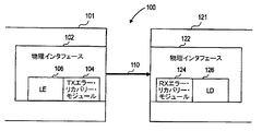
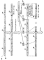
図1Aは、本発明の少なくとも1つの特定的な実施形態によりエラー・リカバリー・モジュールを含んでライン符号化/復号化に関連してエラーを検出する物理インタフェースを示すブロック図100である。物理インタフェース102及び122は、装置101及び121の間の物理的接続性を提供するものであり、その各々は、メモリチップのような集積回路か、又は「イーサネット」ラインカード又はネットワーク化コンピュータのような電子装置とすることができる。物理インタフェース102及び122は、物理的媒体110を通じてデータビットの送受信を容易にするために、それぞれ、ライン符号器(LE)106とライン復号器(LD)126を含む。一実施形態では、ライン符号器(LE)106は、ライン符号化(「ラインコード化」とも呼ばれる)を提供するものであり、これは、銅線、光ファイバ、無線波のような特定の種類の媒体上の符号化データビットの送信を最適化するための特定のコード(又はコード語)へのバイナリ(すなわち、データビット)で表されたデジタル情報の変換である。ライン復号化は、特定のコードからデータビットに変換する逆の処理である。ライン符号器及びライン復号器の両方は、特定の種類の媒体と共に最適に作動するように調整される。一部の実施形態において使用されるように、符号化という用語は、コード語へのデータビットの変換、並びにコード語への又はコード語によるデータビットの挿入を意味する。
FIG. 1A is a block diagram 100 illustrating a physical interface that detects errors associated with line encoding / decoding including an error recovery module in accordance with at least one specific embodiment of the present invention. The
物理インタフェース102はまた、送信器(TX)エラー・リカバリー・モジュール104を含み、一方、物理インタフェース122はまた、受信器(RX)エラー・リカバリー・モジュール124を含む。両方のエラー・リカバリー・モジュール104及び124は、エラーを検出し、かつライン符号化又は復号化に関連して又はそれと共に上述のエラーを任意的に訂正するように作動する。図1Aは、一方向の通信を示すが、当業者は、TXエラー・リカバリー・モジュール104及びRXエラー・リカバリー・モジュール124の構造及び/又は機能を組み合わせて送受信機(TX/RX)エラー・リカバリー・モジュール(図示せず)を形成し、物理的媒体110を通じて双方向通信中にエラー検出及び訂正をサポートすることができることを認めるべきである。少なくとも1つの実施形態では、物理的媒体110は、シリアルデータリンクを提供する。データリンクがシリアルデータリンクであるか又はパラレルデータリンクであるかに関係なく、ライン符号器106及びライン復号器126は、ライン符号化/復号化を実施して、(1)データストリーム内に組み込まれたクロックを回復するために適切な回数の遷移がデータストリーム内にあることを保証し、(2)d−c均衡を維持し、かつ(3)データリンクのスペクトル成形を提供して電磁気放出を低減することのうちの1つ又はそれよりも多くを行う。
The
特定的な実施形態では、エラー・リカバリー・モジュール104及び124は、例えば、ライン復号化の前、最中、又は後のいずれかの時間にエラー検出を提供することができるように、データビットが受信器(例えば、IC又は電子装置)に到着した直後の早期のエラー検出を容易にする。従って、物理インタフェース124内のエラー検出は、エラー検出及び訂正技術を適用することができるまで、装置121が正しくないか又は破損したデータビットで不必要に他の下流側処理を実行するのを防止することができる。有利な態様においては、エラー・リカバリー・モジュール104及び124は、コンピュータリソースを保存しなければ破損データビットを処理する場合があるコンピュータリソースを保存し、また、本発明の様々な実施形態に従ってエラーを検出及び/又は訂正するのに必要とされる時間を短縮することにより、装置101及び121間の通信を容易にすることができる。また、本発明の様々な特徴により、エラーを検出する時間を短縮することができる。例えば、エラー検出ビットは、従来のように、送信されるデータビットの群の終わりにではなく、アプリケーションデータビットと交互に織り込んで転送することができる。少なくとも1つの実施形態では、ライン符号器106は、シリアルデータリンクに対してデータストリームを符号化するためにNB/(N+2)Bライン符号化を使用する。更に、ライン符号器106は、アプリケーションデータビットが物理的媒体110上で通信される速度に影響を及ぼすことなく物理インタフェース(PI)エラー訂正ビットをその符号化データストリーム内に組み込むように作動することができる。有利な態様においては、物理インタフェース102及び122は、全体的又は部分的を問わず、物理層(又は「PHY」)において、エラーを解決するために装置101及び121を必要とすることなく、下位でのエラー検出及び/又は訂正を提供することができる。従って、装置101及び121の作動に対して透明であるように、アプリケーションデータビットと共にPIエラー訂正情報を伝送することができる。言うまでもなく、装置101及び121の場合のエラー検出及び/又は訂正は、物理インタフェース102及び122を超えた回路及び/又は層での他のエラー・リカバリー技術によって補うことができる。従って、アプリケーションデータビットは、上部層エラー・リカバリー機構のための上部層(UL)エラー検出ビットを含むことができる。エラー検出及び/又は訂正は、物理層で行われるので、エラー検出は、有利な態様においては、物理インタフェース102及び122を超えて行われる場合よりも迅速に行うことができる。
In particular embodiments, the
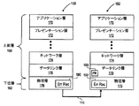
図1Bは、本発明の1つ又はそれよりも多くの実施形態によりデータリンク層ではなく物理層でエラー検出を提供するように実行される図1Aのエラー・リカバリー・モジュール104及び124を示している。「国際標準化機構(ISO)開放型システム相互接続基準モデル(OSIモデル)」では、物理層(例えば、下位層162)及びデータリンク層176を含む他の上部層160の機能性が説明されている。図1Bは、装置101のためのOSIモデル150と、装置121のためのOSIモデル152とを示している。特に、OSIモデル150及び152の各々は、アプリケーション層170、プレゼンテーション層172、ネットワーク層174、データリンク層176、及び物理層178の1つ又はそれよりも多くを含み、その全ては、公知でありかつここで詳細に説明する必要がない機能性を有する。OSIモデル150によれば、送信IC又は装置101(すなわち、「送信器」)のデータリンク層176は、一般的に、下位層162においてライン符号器による符号化の前に上位エラー検出コードを発生させ、一方、受信IC又は装置121(すなわち、「受信器」)のデータリンク層176は、通常、下位層162ライン復号器がライン符号化ビットを復号化した後にエラーを検出して訂正する。特に、受信データリンク層176は、通常、復号化データビットのビットストリームをフレームに組み立てて、次に、フレームのコンテンツに基づいてCRC検査のような上位エラー検出コードを計算する。一例においては、フレーマー(FR)193は、ビットの連続した組をフレームに組み立てる。特に、フレーマー193は、フレームのフィールドの1つにおいて「フレーム検査シーケンス(FCS)」コードを確立する。FCSは、例えば、巡回冗長検査(CRC)チェックサムを使用してエラーを検出するのに使用される。FCSは、通常、CRC検査と突き合わせてエラーが存在するか否かを判断する。説明のために、「イーサネット」フレームが、ヘッダビット及び1500バイトまでのペイロードを含み、CRC検査が32個の連続ビットとしてペイロード端部に添付されていると考える。一般的に、CRC検査は、物理層178よりも上にある1つ又はそれよりも多くの上部層160内に添付される。図示のように、物理層178は、少なくとも一部の実施形態では、下位層162が上部層160内で採用されたあらゆる上位エラー・リカバリー機構に関係なく下位エラー検出及び/又は訂正(エラー・リカバリー)を提供することを可能にするために、下位エラー・リカバリー機能(Err Rec)190及び192を含む。少なくとも1つの実施形態では、下位エラー・リカバリー機能(Err Rec)190及び192は、全体的又は部分的を問わず、エラーが発生したか否かを判断するために、バッファ(例えば、FIFOバッファ)内にアプリケーションデータビットが一時的に記憶される前に又は記憶中に作動する。エラーが存在しない場合、アプリケーションデータビットは、ビットの部分集合への組立てのために上部層に放出される。ビットの部分集合は、「イーサネット」フレーム、メモリ装置のアドレスなどを表すことができる。特定的な実施形態では、物理層178とデータリンク層176の間の境界は、アプリケーションデータビットが組立てのためにバッファを出て上部層に向かう点となっている。
FIG. 1B shows the
どの層が従来のエラー検出及び訂正を実行するかに関係なく、従来の上位エラー検出コードは、一般的に、ペイロードと類似の方法で送信される。しかし、本発明の様々な実施形態によれば、下位エラー検出コード及びペイロードは、パラレルのような異なる方法でライン復号化することができる。本明細書で使用される時、ペイロードという用語は、一般的に、アプリケーション層によって使用されるプログラム命令及び/又はプログラムデータを表すビットの集まり(すなわち、アプリケーションデータビット)を意味する。アプリケーションデータビットは、アプリケーションデータを構成し、従って、データビット転送を制御する制御コードを含まない。それに反して、検出コードは、データビット送信の信頼性を制御するのに使用されるので制御コードである。従って、様々な実施形態によれば、アプリケーションデータビットとエラー検出ビットの両方の一部分は、同時に又はほぼ同時にライン復号化される(かつライン符号化される)(特にアプリケーションデータビットとエラー検出ビットの両方の一部分を共に符号化してコード語を形成する場合)。一実施形態では、ライン復号器は、コード語を変換して復号化データビットを形成するように作動し、復号化データビットは、アプリケーションデータビットと物理インタフェース(PI)エラー検出ビットの両方を含むことができる。従来の上位エラー検出コードは、連続ビットの群(例えば、「イーサネット」フレームのためのCRC検査のビット)として送信され、通常、ライン復号器を通じてアプリケーションデータビットと類似の方法で上部層に渡されることに注意されたい。その結果、従来の上位エラー検出技術では、一般的に、コンピュータリソースを浪費して上位層でのエラー・リカバリーのために制御コードをライン復号化し、一方、本発明の少なくとも特定的な実施形態によれば、下位エラー検出コードは、物理層へ以外にはどこにも伝達される必要がない。 Regardless of which layer performs conventional error detection and correction, conventional upper error detection codes are generally transmitted in a manner similar to the payload. However, according to various embodiments of the present invention, the lower error detection code and the payload can be line decoded in different ways, such as in parallel. As used herein, the term payload generally refers to a collection of bits (ie, application data bits) that represent program instructions and / or program data used by the application layer. Application data bits constitute application data and thus do not include control codes that control data bit transfer. On the other hand, the detection code is a control code because it is used to control the reliability of the data bit transmission. Thus, according to various embodiments, a portion of both application data bits and error detection bits are line decoded (and line encoded) at the same time or nearly simultaneously (particularly of application data bits and error detection bits). If both parts are encoded together to form a codeword). In one embodiment, the line decoder operates to convert codewords to form decoded data bits, where the decoded data bits include both application data bits and physical interface (PI) error detection bits. be able to. Conventional upper error detection codes are transmitted as a group of consecutive bits (eg, CRC check bits for an “Ethernet” frame) and are usually passed to the upper layer in a manner similar to application data bits through a line decoder. Please note that. As a result, conventional upper error detection techniques generally waste computer resources and line decode the control code for error recovery in the upper layer, while at least specific embodiments of the present invention. Thus, the lower error detection code does not need to be transmitted anywhere other than to the physical layer.
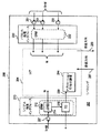
図2Aは、本発明の一実施形態によりエラー・リカバリー・モジュールを実行して組込クロック及びクロック・リカバリーを使用する物理インタフェースで確実なデータ転送を提供する回路のブロック図である。図示の例においては、電子装置200は、それぞれ、RXエラー・リカバリー・モジュール(ERM)212及びRXエラー・リカバリー・モジュール(ERM)232から成る物理インタフェース210及び230を含む。尚、図2AではTXエラー・リカバリー・モジュールを含む物理インタフェースが割愛されているが、当業者は、このようなTXエラー・リカバリー・モジュールも実行することができるが機能性が逆であることを認めるべきである。一部の場合では、物理インタフェース210及び230は、例えば、入力/出力(I/O)リング202内の回路として形成される。I/Oリング202は、結合ワイヤのような導体を、信号をコア回路204に送信する集積回路のような外部信号発生源(図示せず)に結合する入力端子及び出力端子を含む。RXエラー・リカバリー・モジュール212及びRXエラー・リカバリー・モジュール232は、コア回路に信号を送出するためにコア回路204に結合される。一部の実施形態で使用される時、コア回路という用語は、1つ又はそれよりも多くのコア機能を実行しかつ物理インタフェース210及び230を通じて入力を受信又は入力を送出するように構成することができるあらゆる種類の回路を意味する。一部の実施形態では、コア回路204は、知的財産(IP)コアから形成することができ、知的財産(IP)コアは、ハードウエア説明言語(HDL)コード(例えば、「VHDL」又は「Verilog」)で又はネットリストファイルとして表すことができる。従って、コア回路204は、携帯式であるので、物理インタフェース210及び230によって行われる下位層エラー検出及び訂正から恩典を受ける殆どの設計に容易に挿入することができる。一例として、コア回路204は、動的ランダムアクセスメモリ(DRAM)、マイクロコントローラ又はプロセッサ回路、又は物理インタフェースでのエラー検出及び訂正の実行から恩典を受けるようなあらゆる種類の回路のようないずれかの回路であると考える。有利な態様においては、下位エラー検出及び訂正は、コア回路204に対して透明である方法で作動する(すなわち、物理インタフェースエラー・リカバリーでは、エラー検出及び/又は訂正を提供するコア回路204のリソースが必要でなくてもよい)。
FIG. 2A is a block diagram of a circuit that implements an error recovery module to provide reliable data transfer over a physical interface that uses an embedded clock and clock recovery in accordance with one embodiment of the present invention. In the illustrated example, the
物理インタフェース210は、N+m個の符号化ビットを受信してライン復号器エラー検出器(LD/ED)214に入れ込むように構成されたシリアル物理インタフェースであり、ライン復号器エラー検出器(LD/ED)214は、N+m個の符号化ビットの全て又は一部を復号化してN個の復号化アプリケーションデータビットを形成するように構成される。「m」の値は、符号化データビット数とアプリケーションデータビット数に基づくビット数の差を表している。例えば、8B/10Bライン符号器は、2というmを有し、2というmは、差である。ライン復号器エラー検出器214は、符号化ビットをライン復号化し、次に、エラーが検出可能である場合はエラーを検出するように作動する。ライン復号器エラー検出器214がエラーを検出した場合、エラー訂正器(EC)216にエラー・リカバリー対策を講じるように指示する。一実施形態では、エラー訂正器216は、エラー表示信号218を外部IC又は装置に送信して、N+m個の符号化ビットを物理インタフェース210に再送信することなどによりエラーを解決することができるように外部IC又は装置に警告するように構成される。有利な態様においては、物理インタフェース210及び230は、コア回路204を修正することなく、エラー検出及び訂正をコア回路204に対して行うことにより、エラー検出又は訂正をコア204に統合するために必要とされるエンジニアリングリソースが保存される。別の実施形態では、エラー訂正器216は、エラーを訂正することができるように、エラー表示信号220をコア回路204に送信するように構成される。この場合、コア回路204は、アプリケーション特有の論理244を含んであらゆる検出エラーを訂正する。有利な態様においては、従って、コア回路204(又は他の場所)におけるアプリケーション特有の論理244によるエラー処理により、エラー検出及び訂正が可能になり、エラー訂正を容易にする送信IC又は装置(図示せず)が不要になる。それによって、特に、半導体パッケージに封入された場合、電子装置200が必要とする信号導体及び/又はピンの数が最小限に抑えられる。更に別の実施形態では、物理インタフェース210のエラー訂正器216は、いずれかのエラー表示信号218又は220を送ることなくエラーを訂正することができる。例えば、エラー訂正器は、自動的にエラーを訂正する順方向のエラー訂正器技術を実行することができる。
The
次に、外部ICが、例えばDRAMコントローラ(図示せず)であり、コア回路204が、DRAMメモリであると考える。そこで、物理インタフェース230は、チップ間インタフェースとなって、エラー訂正後のアドレス及びデータをDRAMコントローラ及びDRAMメモリ(すなわち、コア回路204)間で交換することができ、その1つ又はそれよりも多くは、エラー検出及び訂正を提供するようには修正されない(機能的又は構造的に)。一部の実施形態では、物理インタフェース210及び230は、第1の基板上に形成され、第1の基板は、入力/出力(I/O)リング202を含む。コア回路204は、第2の基板上に形成される。第1及び第2の基板が別々のものである場合、物理インタフェース210及び230は、コア回路204から分離してパッケージ化することができる。しかし、同じ基板上に形成された場合、システムオンチップ(SOC)の一部として形成することができ、かつ、単一のパッケージによって共に封入することができる。代替的な実施形態では、物理インタフェース230は、N+m個の符号化ビットを受信してRXエラー・リカバリー・モジュール232に入れ込み、次に、N+m個の符号化ビットの一部又は全てを復号化してN個の復号化アプリケーションデータビットを形成するように構成されたパラレル物理インタフェースである。図2Aでは、説明する内容を簡素化するために、RXエラー・リカバリー・モジュール232のライン復号器エラー検出器及びエラー訂正器の詳細は割愛されている。図2Aは、着信データビット(すなわち、コア204のために着信)を着信方向に供給する物理インタフェース210及び230を示すものであることに注意されたい。上述と同じ物理インタフェースは、発信方向298のコア204からの発信データビット送信(図示せず)を提供することができる。シリアル物理インタフェース210及びパラレル物理インタフェース230のいずれも、着信データビットをライン復号化し、特に、その中の組込クロックを回復するように構成されることに注意されたい。他の実施形態では、シリアル物理インタフェース210又はパラレル物理インタフェース230のいずれか又は両方は、組込クロックではなく外部クロックを受信するように構成することができる。
Next, it is considered that the external IC is, for example, a DRAM controller (not shown), and the
図2Bは、本発明の一実施形態によりエラー・リカバリー・モジュールを実行して確実なデータ転送を外部クロックを使用する物理インタフェースにおいて行う図2Aの回路の別のブロック図である。図2Aのシリアル物理インタフェース210又はパラレル物理インタフェース230とは異なって、図2Bの電子装置200は、外部クロック(Ext.CLK)274を受信するように構成されたシリアル物理インタフェース250を含む。また、電子装置200は、外部クロック(Ext.CLK)254を受信するように構成されたパラレル物理インタフェース270を含む。両方の物理インタフェース250及び270は、外部クロック信号を受信することができるので、これらのインタフェースは、組込クロック技術を採用する必要がなく、従って、クロック・リカバリー回路を含む必要がない。従って、エラー・リカバリー・モジュール252及び272は、ライン復号器又はライン復号化処理の後に配置する必要がない。図2Bの要素は、各々、図2Aの類似の付番を有する要素と同等の機能性及び/又は構造を有することができることに注意されたい。
FIG. 2B is another block diagram of the circuit of FIG. 2A that executes an error recovery module according to one embodiment of the present invention to perform reliable data transfer at a physical interface using an external clock. Unlike the serial
図3は、本発明の特定的な実施形態によりエラーを検出しかつ任意的に訂正するように構成された物理インタフェースを示すブロック図である。物理インタフェース300は、物理層(PHY)ライン復号器302とエラー・リカバリー・モジュール310とを含み、エラー・リカバリー・モジュール310は、エラー検出ビット抽出器312、エラー検出器314、及びエラー訂正器316から成る。エラー検出ビット抽出器312は、少なくともPHYライン復号器302と機能的に協働し、従って、図3においては、PHYライン復号器302内にあるように示されている。この例においては、PHYライン復号器302は、少なくとも、ビットストリームのN+m個の符号化ビット(すなわち、符号又はコード語)を受信し、かつ上述のビットの全て又は一部を復号化してN個の復号化アプリケーションデータビットを形成するように構成される。例えば、PHYライン復号器302は、10個、14個、20個、66個、又は130個の符号化アプリケーションデータビット(すなわち、「N+2」ビット)を受信するように作動することができ、次に、それぞれ、上述のビットを復号化して8個、12個、18個、64個、又は128個の復号化アプリケーションデータビット(すなわち、「N」ビット)を形成することができる。少なくともクロック・リカバリー及びDC均衡化には、2つのビットが使用されてきた。様々な実施形態では、PHYライン復号器302は、あらゆる数の符号化データビットを受信し、次に、上述のビットをあらゆる他の数のアプリケーションデータビットに復号化するように作動することができる。例えば、PHYライン復号器302は、80ビットの符号化データを復号化して64個の復号化アプリケーションデータビットを形成することができる。
FIG. 3 is a block diagram illustrating a physical interface configured to detect and optionally correct errors according to a particular embodiment of the present invention. The
特定的な実施形態では、PHYライン復号器302は、N+m個のビットの部分集合であるN+m−1個の符号化ビットを復号化して、N個の復号化アプリケーションデータビットとE個のエラー検出ビットを生成する。次に、ビット抽出器312は、下位エラー検出のために1つ又はそれよりも多くの物理インタフェースエラー検出ビットを抽出する。例えば、エラー検出ビット抽出器312は、単一のビットをN+m個(例えば、10個のビット)という数量から抽出してN+m−1個のビット(例えば、9個のビット)復号化ビットを生成することができるが、N+m−1個のビット(例えば、9ビット)復号化ビットは、N個の復号化アプリケーションデータビットとE個の復号化エラー検出ビットとを含む。従って、PHYライン復号器302は、N+m個のビットを受信し、かつライン復号化を提供するように構成され、それによってN個のアプリケーションデータビットと少なくとも1つのエラー検出ビットが得られる。有利な態様においては、PHYライン復号器302は、従来の10B/8B復号器を補うか又は従来の10B/8B復号器に取って代わるように実行することができるが、従来の10B/8B復号器は、符号化ビットに対しては10ビットという一般的に使用される符号サイズを使用し、復号化アプリケーションデータビットは、8ビットというビットサイズを有する。本発明の様々な実施形態では、PHYライン復号器302は、9番目のビット(すなわち、10個の符号化アプリケーションデータビットと8個の復号化アプリケーションデータビットの間の差の2ビットの一方)を検査してエラーを検出する。適切なPHYライン復号器302は、「NB/(N+1)Bブロックコードに従ってデータを符号化又は復号化する方法及び機器、及びこのようなブロックコードを判断する方法」という名称の米国特許第6,747,580号で説明されているようなN+1ビット/Nビット復号器であり、この特許の内容全体は、引用により全ての目的に対して組み込まれている。尚、図3は、PHYライン復号器302を示すが、当業者は、図3及び本明細書の他の場所で説明するのと逆の方法で作動するようにN個のアプリケーションデータビットとE個のエラー検出ビットとをN+m個の符号化ビットに符号化するPHYライン符号器(すなわち、Nビット/N+mビット符号器)を構成することができることを認めるべきである。
In a specific embodiment, the
抽出後、エラー検出ビット抽出器312は、次に、物理インタフェース(PT)エラー検出ビット(EDB)313をエラー検出器314に送り、エラー検出器314は、そのビットを使用してN+m個の符号化データビットが1つ又はそれよりも多くの誤ったデータビットを含むか否かを判断する。エラー検出器314は、いずれかの数のエラー検出技術及びコードに従ってエラーを検出するように構成される。一実施形態では、エラー検出器314は、偶数又は奇数パリティチェッカーとして構成され、物理インタフェースエラー検出ビットは、パリティビット(すなわち、偶数又は奇数のパリティビット)である。有利な態様においては、物理インタフェースエラー検出ビットは、復号化されるアプリケーションデータビットの部分集合と同時にPHYライン復号器302で受信される。それによって、符号化データビットの群がN+m個のビットよりも遥かに大きいサイズを有する可能性がある場合は、エラー検出コードをその群の端部に添える従来のエラー検出技術と比較すると、PHYライン復号器302がエラー検出コードを受信するのに必要とされる時間量を低減することができる。別の実施形態では、物理インタフェースエラー検出ビットは、CRC検査の一部(例えば、1ビット)である。この場合、送信物理インタフェース(図示せず)におけるエラー検出コード発生器は、物理インタフェースエラー検出ビットをCRC検査の一部として発生させるように構成される。図6で以下に説明するように、エラー検出コード発生器(又は均等物)は、CRC検査のビットをPHYライン符号器(図示せず)に供給することができる。PHYライン符号器は、物理インタフェースエラー検出ビットをN個の未符号化アプリケーションデータビットと共に挿入してN+2個の符号化データビットを生成する。その結果、エラー検出器314は、N+m個の復号化データビットの各部分集合からの物理インタフェースエラー検出ビットを蓄積するか又は収集し、CRC検査をエラー検出コードとして再構成するように作動する。例えば、PHYライン復号器302によって復号化される10個の符号化ビットの各組に対して、CRC検査の1ビットが8個の復号化アプリケーションデータビットの各組に対して物理インタフェースエラー検出ビットとして供給されると考える。16ビットのCRC検査が実行された場合、8個の復号化アプリケーションデータビットの16組毎に(すなわち、128ビット毎に)、エラー検出器314CRCは、160ビットCRC検査を再構成することができる。次に、エラー検出器314は、上述の128ビットからCRC検査を発生させ、次に、CRC検査を再構成エラー検出コードと突き合わせてエラーが発生したか否かを判断する。エラー検出器314は、順方向エラー訂正のような他のエラー検出技術を実行することができる。順方向エラー訂正技術の例としては、「Reed−Solomon」コード、「Hamming」コード、及び「Bose−Chaudhuri−Hocquenghem(BCH)コードがある。
After extraction, the error
エラー検出器314がデータビット送信中にエラーが発生したと判断した状態で、このようなエラーが発生したことをエラー訂正器316に知らせる。一部の場合では、エラー訂正器316は、エラーが検出された復号化アプリケーションデータビットの再送信を要求するように作動する。先の例に続いて、16ビットCRC検査の比較でエラーが128個の復号化アプリケーションデータビット内に存在することが分った場合、エラー訂正器316は、送信物理インタフェースが上述の128ビットを再度送るように要求することができる。他の場合には、エラー訂正器316は、アプリケーション特有の回路を起動させて、ユーザによって構成されたエラー処理を提供することができる。少なくとも1つの事例においては、エラー訂正器316は、上述のコア回路のような関連ICを再初期化するなどの何らかの種類のデフォルトエラー訂正措置を講じることができる。
When the
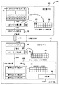
図4は、本発明の一実施形態によりエラー検出ビット挿入及び抽出を備えた送信器におけるライン符号化及び受信器におけるライン復号化を示す機能ブロック図である。図400に示すように、送信器物理インタフェース(TX)410は、例えば、PHYライン符号器412と、エラー検出コード発生器416と、エラービット挿入器418と、エラー検出コード発生中にアプリケーションデータビットを維持する任意的なバッファ421とを含む。この例においては、エラー検出コード発生器416は、16ビットCRC検査のようなバッファ421におけるアプリケーションデータビットに基づいて、エラー検出コードを発生させる。次に、エラービット挿入器418は、少なくとも1つのエラー検出ビット(EDB)414を16ビットCRC検査から選択し、次に、バッファ421からのN個のアプリケーションデータビットの発信組と共に挿入して9ビットを形成する。次に、PHYライン符号器412は、9ビットを10個の符号化ビット(又は記号)に符号化する。一部の実施形態では、PHYライン符号器412は、10個の符号化ビットに関するゼロDCオフセット及び/又は任意的なスペクトル特性を維持すると共に、上述の10個の符号化ビット内に非同期クロックを組み込むような方法でエラー検出ビット414を符号化する。特定的な実施形態では、PHYライン符号器412は、米国特許第6,747,580号に定めるコード化技術に従って作動することにより、NビットのアプリケーションデータをN+1個の符号化ビットに符号化する。例えば、Nが数字9であると考える。従って、PHYライン符号器412は、8B/10Bコード化技術に関連したデータ転送速度に影響を与えることなく、8個のアプリケーションデータビットと1個のエラービット(すなわち、9ビット)とを10個の符号化ビットに符号化することができる。図4において、Nは、あらゆる負以外の整数を表すことができることに注意されたい。
FIG. 4 is a functional block diagram illustrating line coding at the transmitter and line decoding at the receiver with error detection bit insertion and extraction according to one embodiment of the present invention. As shown in FIG. 400, a transmitter physical interface (TX) 410 includes, for example, a
次に、送信器物理インタフェース410は、物理的媒体420を通じて符号化ビットを受信物理インタフェース(RX)440のエラービット抽出器422に送る。受信物理インタフェース(RX)440は、PHYライン復号器428と、エラービット抽出器422と、エラー検出コード再構成器426と、エラー検出器430と、比較器434と、エラーが検出されていないという復号化アプリケーションデータビット未決確認を維持することができるバッファ431とを含む。PHYライン復号器428は、10個の符号化データビットを9個の復号化ビットに復号化し、9個の復号化ビットは、8個の復号化アプリケーションデータビットと1個の復号化エラー検出ビット(EDB)424を含む。様々な実施形態では、PHYライン復号器428は、クロックデータリカバリー回路(図示せず)を含んで符号化アプリケーションデータビットと共に物理的媒体420で送信された組込クロックを回復する。エラービット抽出器422は、エラー検出ビット424を9個の復号化ビットから抽出してエラー検出コード再構成器426に供給し、エラー検出コード再構成器426は、他の物理インタフェースエラー検出ビットと共にエラー検出ビットを蓄積する。次に、エラー検出コード再構成器426は、元々エラー検出コード発生器416が発生させたエラー検出コードを再構成する。次に、エラー検出器430は、バッファ431におけるN個の復号化アプリケーションデータビットの群に基づいてCRC検査432を発生させる。比較器434は、CRC検査432がエラー検出コード426に適応するか否かに関して比較するように作動することができる。適応した場合には、エラーがなく、適応しなかった場合には、エラーがある。
The transmitter
図5は、本発明の一実施形態に従ってセルとしてデータビットの群をライン符号化するフローの一例を示している。一部の実施例においては、送信器物理インタフェースは、フロー550に示すようにデータを送信することができ、それによってデータビットの群560は、セル(並びにフレームなど)と呼ぶことができる。セル560は、例えば、あらゆる数の制御ビット561(例えば、X個のビット)と、各々が64ビットの2個のアプリケーションデータ語563とを含むことができる。物理層内でPHYライン符号器の上方にある上部層装置(図示せず)は、セル560がPHYライン符号器によって使用されるように、個別の組562のコード化されていない(すなわち、予めコード化されているか又はコード化されていない)ビットに分解するように構成することができる。各組562は、N個のビット(例えば、8ビット)を有する。エラー検出コード発生器(図示せず)は、例えば、セル560に基づいてエラー検出コード570を発生させ、エラー検出コードを12ビットのCRCとして形成する。次に、PHYライン符号器は、物理インタフェースエラー検出ビット(EDB)572を組562内又は組562の近くでコード化されていないビットストリームに挿入し、N+E個のビット(例えば、Nは、8ビットとすることができ、Eは、1ビットとすることができる)の組574を形成することができる。次に、PHYライン符号器は、シリアルデータリンクのようなデータリンク上で送信されるように、N+E個のビットの各組572を10ビットのコード語580(例えば、符号化データビット)に変換することができる。図示していないが、受信物理インタフェースでのPHYライン復号器は、類似であるが逆に作動することになる。
FIG. 5 shows an example of a flow for line encoding a group of data bits as cells according to one embodiment of the present invention. In some embodiments, the transmitter physical interface can transmit data as shown in
図6は、本発明の少なくとも1つの特定的な実施形態により少なくとも再送信データビットによるエラー検出及び訂正を提供する物理インタフェースを示すブロック図600である。物理インタフェース602及び652は、高速シリアル通信リンク650を通じて物理的接続性を提供する。物理インタフェース602は、送信されるデータビットを記憶するために先入れ先出しバッファ(FIFO)604のような記憶装置を含む。FIFO604は、例えば、データビットの群にわたってエラー検出コードを計算するために記憶データビットを維持する。一部の場合では、FIFO604は、エラーが発生した場合に再送信されるようにデータビットを記憶する。また、物理インタフェース602は、PHYライン符号器(PHY符号器)610と、パラレルデータビットをシリアル化するシリアライザ(SER)612と、エラー検出コード発生器616と、送信器(TX)エラー訂正器618とを含む。特定の時間でのFIFO604内のデータビットの群のコンテンツに基づいて、エラー検出コード発生器616は、CRC検査のようなエラー検出コードを発生させる。エラー検出ビット挿入器614は、CRC検査を分解し、N個の未符号化ビット606と共に物理インタフェースエラー検出ビット(EDB)として少なくとも1つのビット(例えば、1つのEビット)を挿入する。作動においては、PHYライン符号器610は、N+E個のビットを符号化してN+2個の符号化データビット608を形成する。次に、シリアライザ612は、リンク650での送信の前にN+2個のデータビット608をシリアル化する。受信物理インタフェース652は、デシリアライザ654を含んでN+2個のデータビットをパラレルデータビットに変換する。PHYライン復号器(PHY復号器)656は、符号化ビットストリームを復号化して復号化データビットをFIFO658に記憶する。エラー検出ビット(EDB)抽出器660は、少なくとも1ビットを物理インタフェースエラー検出ビット(EDB)662として抽出してエラー検出器666に送る。エラーコード再構成が完全である場合、エラー検出器666は、エラーが発生したか否かを判断するように作動する。エラー検出器666がエラーなしと判断した場合、更に別の処理のために復号化データビットを放出するようにFIFO658に指示する。しかし、エラー検出器666がエラーを検出した場合、受信器(RX)エラー訂正器668に対してエラーの存在を表示する。一例においては、RXエラー訂正器668は、TXエラー訂正器618にリンク650を通じてコンテンツ又はその一部を再送信するように指示する要求669を送る。別の例においては、RXエラー訂正器668は、エラーを処理する要求671をアプリケーション特有の回路(図示せず)に送ることができる。更に別の例においては、受信器エラー訂正器668は、順方向エラー訂正技術などを使用してエラーを訂正することができる。
FIG. 6 is a block diagram 600 illustrating a physical interface that provides error detection and correction with at least retransmission data bits in accordance with at least one specific embodiment of the present invention.
図7は、本発明の少なくとも1つ特定的な実施形態によりライン復号化なしにエラー検出及び訂正を実行する代替的受信器を示している。受信器(RX)700においては、送信器物理インタフェース(図示せず)は、リンク702を通じてデータビットを送る。エラービット抽出器704は、エラー検出データビット(EDB)706をデータビットから抽出してエラー検出コード708を再構成する。図4の図400とは異なって、受信器700は、受信器440のようにはPHYライン復号器を使用しない。従って、受信器700は、クロック信号を組込クロックから回復する必要がない。図示のように、受信器700は、外部クロック701を例えば送信装置(図示せず)から受信するように構成される。リンク702での送信の前に、例えばエラー検出ビットをアプリケーションデータビットに添えるのは、この送信装置である。受信器700は、FIFO720内のアプリケーションデータビットの群に基づいて、検出コード、すなわち、この場合はCRC検査722を計算するために、エラー検出器780を含む。次に、比較器724(例えば、エラー検出器720において)は、送信エラーが発生したか否かを判断する。エラーが存在する場合、エラー訂正器780は、例えば、送信装置にデータビットを再送信するように要求するか又はエラーを訂正すべきであることをアプリケーション特有の論理に知らせることによって是正措置を講じることができる。
FIG. 7 illustrates an alternative receiver that performs error detection and correction without line decoding in accordance with at least one specific embodiment of the present invention. In receiver (RX) 700, a transmitter physical interface (not shown) sends data bits over
図8は、本発明の一実施形態によるエラー訂正器のブロック図を示している。エラー訂正器800は、この例においては、エラー訂正器コントローラ822を含んでエラーを解決することができる1つ又はそれよりも多くの機能を制御し、特定の機能は、特定の用途に対してユーザによってプログラムされる。例えば、ビデオメモリ用途でのピクセルデータの損失は、他の用途におけるデータ損失ほど重要なものではない。従って、エラー訂正器コントローラ822は、以下のモジュールのいずれかを選択してエラー訂正を実行することができる。再送信要求モジュール824は、エラーを検出するとデータビットを再度送るために送信器物理インタフェース行きの要求を発生させる。アプリケーション特有のリカバリーモジュール814は、設計担当者によって指定されるような特注のエラー処理ルーチンを開始するようにアプリケーション特有の回路に知らせる。しかし、エラー訂正器コントローラ822は、エラーを検出すると、ICを再度初期化するなどのデフォルトエラー・リカバリー技術を選択することができる。それによって両方の物理インタフェースは、既知の状態に再度初期化されることになる。様々な代替的な実施形態では、エラー訂正器800は、周波数セレクタ830と、振幅セレクタ840と、コード化セレクタ850とを含むことができる。物理インタフェース間の通信リンク上の信号が行き詰った場合、周波数セレクタ830は、リンク上のデータ転送速度を調節してエラー率を低減することができる。代替的に、振幅セレクタ840は、エラー率が低減されるまで信号振幅を調整することができる。コード化セレクタ850を使用すると、リンクコード化を例えば18B/20Bから8B/10Bに変更して、エラーが検出される時間を短縮することができる。例えば、32ビットのCRCがエラー・リカバリーに実行され、一度にCRCの1ビットが送られると考える。18B/20Bでは、32ビットのCRC(すなわち、8*32=576ビット)を形成するのに576個のアプリケーションデータビット(8ビット)が必要であり、一方、8B/10Bでは、256個のアプリケーションデータビットが必要である。従って、コード化セレクタ850は、通信チャンネルでエラーコード(例えば、CRC)が送信される率を上げることができる。エラー訂正器コントローラ822は、これらのセレクタを個別に又は組み合わせて選択することができる。
FIG. 8 shows a block diagram of an error corrector according to an embodiment of the present invention. The
説明を目的とした以上の説明では、本発明の徹底的な理解が得られるように特定の名称を使用した。しかし、本発明を実施するためには特定の詳細は必要ではないことが当業者には明らかであろう。実際に、以上の説明は、本発明の何らかの特徴又は態様を何らかの実施形態に限定するものとして読み取るべきではなく、むしろ、一実施形態の特徴及び態様は、他の実施形態と容易に交換することができる。例えば、様々な実施形態の以上の説明は、物理層ライン復号器に関連するが、説明した内容は、物理層ライン符号器及び全ての種類の通信リンク、並びに「ギガビットイーサネット」、HDMI、TMDS、DVI、及びSATAのような多くの種類の通信プロトコルに適用可能である。また、様々な実施形態は、電子装置間のポイントツーポイント通信、並びに1つの装置から多数の装置までのブロードキャストに適用可能である。以上の説明した内容の一部は、シリアルデータ通信に関連するものであるが、本発明の様々な実施形態をパラレルデータ通信にも適用することができる。 In the foregoing description for purposes of explanation, specific names have been used to provide a thorough understanding of the present invention. However, it will be apparent to one skilled in the art that the specific details are not required in order to practice the invention. Indeed, the above description should not be read as limiting any feature or aspect of the invention to any embodiment, but rather features and aspects of one embodiment can be readily interchanged with other embodiments. Can do. For example, while the above description of various embodiments relates to a physical layer line decoder, the described content includes physical layer line encoders and all types of communication links, as well as “Gigabit Ethernet”, HDMI, TMDS, It is applicable to many kinds of communication protocols such as DVI and SATA. Various embodiments are also applicable to point-to-point communication between electronic devices, as well as broadcast from one device to multiple devices. Although some of the contents described above are related to serial data communication, various embodiments of the present invention can also be applied to parallel data communication.
すなわち、本発明の特定的な実施形態の以上の説明は、例示及び説明を目的として示されたものである。網羅的であること又は本発明を開示した形態に正確に限定することを意図したものではない。明らかに、多くの変更及び変形が先の教示内容に鑑みて可能である。実施形態は、本発明の原理及びその実際的な用途を最も良く説明するために選択しかつ説明したものである。その結果、当業者は、考えている特定の用途に適するような様々な修正を行って本発明及び様々な実施形態を最良に利用することができる。明白なことであるが、本明細書で説明する全ての利点が本発明の各実施形態によって達成される必要はない。むしろ、どの特定的な実施形態も上述の利点の1つ又はそれよりも多くをもたらすことができる。特許請求の範囲及びその均等物が、本発明の範囲を規定するものとする。 That is, the foregoing descriptions of specific embodiments of the present invention have been presented for purposes of illustration and description. It is not intended to be exhaustive or to limit the invention to the precise form disclosed. Obviously, many modifications and variations are possible in view of the above teachings. The embodiments have been chosen and described in order to best explain the principles of the invention and its practical application. As a result, one skilled in the art can best utilize the invention and various embodiments with various modifications as appropriate for the particular application under consideration. Obviously, not all advantages described herein need to be achieved by embodiments of the present invention. Rather, any particular embodiment can provide one or more of the advantages described above. The claims and their equivalents shall define the scope of the invention.
100 物理インタフェースを示すブロック図
101、121 電子装置
106 ライン符号器
110 物理的媒体
126 ライン復号器
DESCRIPTION OF
Claims (19)
符号化データビットの部分集合を復号化して復号化データビットを生成するように構成された復号器と、
前記復号化データビットから、前記符号化データビットが少なくとも1つの誤ったデータビットをエラーとして含むか否かを判断するのに使用される物理インタフェースエラー検出ビットを抽出するように構成された物理インタフェース(PI)エラー検出ビット抽出器と、
を含むことを特徴とする機器。 An apparatus for detecting errors in a physical interface that facilitates data communication between integrated circuits (ICs),
A decoder configured to decode a subset of the encoded data bits to generate decoded data bits;
A physical interface configured to extract from the decoded data bits a physical interface error detection bit used to determine whether the encoded data bits include at least one erroneous data bit as an error; (PI) an error detection bit extractor;
A device characterized by including.
を更に含み、
前記符号化データビットの前記部分集合は、組込クロックを含む、
ことを特徴とする請求項1に記載の機器。 An error detector configured to operate in the physical layer to detect the error;
Further including
The subset of the encoded data bits includes an embedded clock;
The device according to claim 1.
前記エラー検出コードは、巡回冗長検査(CRC)チェックサムであり、前記エラー検出器は、前記物理インタフェースエラー検出ビットと、前記符号化データビットの他の部分集合からの他の物理インタフェースエラー検出ビットとを蓄積して該エラー検出コードを再構成するように構成されている、
ことを特徴とする請求項2に記載の機器。 The physical interface error detection bit is part of an error detection code;
The error detection code is a cyclic redundancy check (CRC) checksum, and the error detector includes the physical interface error detection bits and other physical interface error detection bits from another subset of the encoded data bits. And reconstructing the error detection code,
The apparatus according to claim 2.
(1)N個のアプリケーションデータビットと共に物理インタフェースエラー検出ビットを挿入してN+1個の未符号化データビットを形成し、かつ
(2)前記N+1個の未符号化データビットを符号化してN+2個の符号化データビットを生成する、
ように構成されたNビットからN+2(Nビット/N+2)ビット物理層(PHY)符号器と、
前記物理インタフェースエラー検出ビットを含むエラー検出コードを構成するいくつかのビットを発生するように構成されたエラー検出コード発生器と、
を更に含むことを特徴とする請求項1に記載の機器。 N represents any integer number of data bits,
(1) Insert physical interface error detection bits together with N application data bits to form N + 1 uncoded data bits; and (2) N + 2 encoded N + 1 uncoded data bits. Generate encoded data bits of
N bits to N + 2 (N bits / N + 2) bit physical layer (PHY) encoder configured as follows:
An error detection code generator configured to generate a number of bits constituting an error detection code including the physical interface error detection bits;
The device of claim 1 further comprising:
を含み、
前記第1のICは、該第1のICの第1の基板部分上に形成された物理インタフェースを含んで第2の基板部分上に形成された前記第2のICと交換されたデータ内の送信エラーを検出し、
符号化データビットの部分集合を復号化して復号化データビットを生成するように構成された復号器と、
前記復号化データビットから、前記符号化データビットが少なくとも1つの誤ったデータビットをエラーとして含むか否かを判断するのに使用される物理インタフェースエラー検出ビットを抽出するように構成された物理インタフェースエラー検出ビット抽出器と、
を更に含むことを特徴とするシステム。 A first integrated circuit (IC) coupled to a second IC through a physical medium;
Including
The first IC includes a physical interface formed on the first substrate portion of the first IC and includes data in the data exchanged with the second IC formed on the second substrate portion. Detect transmission errors,
A decoder configured to decode a subset of the encoded data bits to generate decoded data bits;
A physical interface configured to extract from the decoded data bits a physical interface error detection bit used to determine whether the encoded data bits include at least one erroneous data bit as an error; An error detection bit extractor;
A system further comprising:
着信符号化データビットを受信するように構成された入力ポートの第1の部分集合と、着信復号化データビットを前記別のICに送信するように構成された出力ポートの第1の部分集合とを含む複数の入力ポート及び出力ポートと、
前記複数の入力ポート及び出力ポートの間に結合された1つ又はそれよりも多くのエラー・リカバリー・モジュールと、
を含み、
前記1つ又はそれよりも多くのエラー・リカバリー・モジュールの第1のエラー・リカバリー・モジュールは、前記第1の部分集合の入力ポートの少なくとも1つと前記第1の部分集合の出力ポートの少なくとも1つとの間に結合されている、
ことを特徴とする請求項7に記載のシステム。 The physical interface is
A first subset of input ports configured to receive incoming encoded data bits; and a first subset of output ports configured to transmit incoming decoded data bits to said another IC; A plurality of input ports and output ports including
One or more error recovery modules coupled between the plurality of input ports and output ports;
Including
The first error recovery module of the one or more error recovery modules includes at least one of the first subset input ports and at least one of the first subset output ports. Connected between the two,
The system according to claim 7.
前記1つ又はそれよりも多くのエラー・リカバリー・モジュールの第2のエラー・リカバリー・モジュールは、前記第2の部分集合の入力ポートの少なくとも1つと前記第2の部分集合の出力ポートの少なくとも1つとの間に結合され、該第2のエラー・リカバリー・モジュールは、前記発信符号化データビットに対するエラー検出コードを発生させるように構成されたPHY符号器を含む、
ことを特徴とする請求項9に記載のシステム。 The plurality of input ports and output ports are configured to transmit a second subset of input ports configured to receive outgoing unencoded data bits from the other IC and outgoing encoded data bits. A second subset of output ports, and
The second error recovery module of the one or more error recovery modules includes at least one of the second subset input ports and at least one of the second subset output ports. And the second error recovery module includes a PHY encoder configured to generate an error detection code for the outgoing encoded data bits.
The system according to claim 9.
前記符号化データビットを復号化するN+2ビット/Nビット復号器、及び
前記物理インタフェースエラー検出ビットを使用してエラーを判断するように構成されたエラー検出器、
を含み、かつ前記物理的媒体の第2の端部に結合された受信装置と、
を更に含むことを特徴とする請求項7に記載のシステム。 Generating encoded data bits, the encoded data bits including an N-bit / N + 2-bit encoder encoded with physical interface error detection bits and coupled to the first end of the physical medium A transmitting device;
An N + 2 bit / N bit decoder for decoding the encoded data bits; and an error detector configured to determine an error using the physical interface error detection bits;
And a receiving device coupled to the second end of the physical medium;
The system of claim 7 further comprising:
組込非同期クロックを有する符号化ビットストリームの部分集合を復号化して復号化データビットを生成する段階と、
前記復号化データビットから物理インタフェースエラー検出ビットを抽出する段階と、
少なくとも前記物理インタフェースエラー検出ビットに基づいて、前記符号化ビットストリームが正しくないビットを含むことを判断する段階と、
前記物理インタフェースにおいて前記エラーを訂正する段階と、
を含むことを特徴とする方法。 A method of decoding data bits and detecting at least an error at a physical interface,
Decoding a subset of the encoded bitstream having an embedded asynchronous clock to generate decoded data bits;
Extracting physical interface error detection bits from the decoded data bits;
Determining that the encoded bitstream includes incorrect bits based at least on the physical interface error detection bits;
Correcting the error at the physical interface;
A method comprising the steps of:
前記物理インタフェースエラー検出ビットを用いて前記符号化ビットストリームの部分集合のパリティを判断する段階と、
前記パリティが所定のパリティと適合しない場合に前記エラーが存在することを示す段階と、
を更に含む、
ことを特徴とする請求項13に記載の方法。 Determining that the subset of the encoded bitstream includes the incorrect bits;
Determining a parity of a subset of the encoded bitstream using the physical interface error detection bits;
Indicating that the error exists if the parity does not match a predetermined parity;
Further including
The method according to claim 13.
前記物理インタフェースエラー検出ビットを他の物理インタフェースエラー検出ビットと組み合わせて第1のエラー検出コードを形成する段階と、
前記復号化データビットからのアプリケーションデータビットと、前記ビットストリームの他の部分集合から復号化された他の復号化データビットからの他のアプリケーションデータビットとに基づいて、第2のエラー検出コードを発生させる段階と、
前記第1のエラー検出コードを前記第2のエラー検出コードに対して比較する段階と、
前記第2のエラー検出コードが前記第1のエラー検出コードと適合しない場合に前記エラーが存在することを示す段階と、
を含む、
ことを特徴とする請求項13に記載の方法。 Determining that the subset of the bitstream includes the incorrect bits;
Combining the physical interface error detection bits with other physical interface error detection bits to form a first error detection code;
A second error detection code based on application data bits from the decoded data bits and other application data bits from other decoded data bits decoded from another subset of the bitstream; Generating stage,
Comparing the first error detection code to the second error detection code;
Indicating that the error exists if the second error detection code does not match the first error detection code;
including,
The method according to claim 13.
Nをデータビットのあらゆる整数を表すものとして、
N個のアプリケーションデータビットと共に物理インタフェースエラー検出ビットを挿入してN+1個の未符号化データビットを形成し、かつ
前記N+1個の未符号化データビットを符号化してN+2個の符号化データビットを生成する、
ように構成されたNビットからN+2(Nビット/N+2)ビット物理層(PHY)符号器と、
前記物理インタフェースエラー検出ビットを含むエラー検出コードを構成するいくつかのビットを発生するように構成されたエラー検出コード発生器と、
を含むことを特徴とする機器。 A device for generating an error detection code at a physical interface for transmission of data communication between integrated circuits (ICs),
N represents any integer number of data bits,
Insert physical interface error detection bits with N application data bits to form N + 1 uncoded data bits, and encode the N + 1 uncoded data bits to generate N + 2 encoded data bits. Generate,
N bits to N + 2 (N bits / N + 2) bit physical layer (PHY) encoder configured as follows:
An error detection code generator configured to generate a number of bits constituting an error detection code including the physical interface error detection bits;
A device characterized by including.
着信符号化データビットを受信するように構成された入力ポートの第1の部分集合と、着信復号化データビットを別のICに送信するように構成された出力ポートの第1の部分集合とを含む複数の入力ポート及び出力ポートと、
前記複数の入力ポート及び出力ポートの間に結合された1つ又はそれよりも多くのエラー・リカバリー・モジュールと、
を含み、
前記1つ又はそれよりも多くのエラー・リカバリー・モジュールの第1のエラー・リカバリー・モジュールは、前記第1の部分集合の入力ポートの少なくとも1つと前記第1の部分集合の出力ポートの少なくとも1つとの間に結合されている、
ことを特徴とする物理インタフェース。 A physical interface for detecting transmission errors in data formed as an integrated circuit (IC) on a first substrate portion and exchanged with another IC formed on a second substrate portion,
A first subset of input ports configured to receive incoming encoded data bits; and a first subset of output ports configured to transmit incoming decoded data bits to another IC. Including a plurality of input ports and output ports;
One or more error recovery modules coupled between the plurality of input ports and output ports;
Including
The first error recovery module of the one or more error recovery modules includes at least one of the first subset input ports and at least one of the first subset output ports. Connected between the two,
A physical interface characterized by
通信データを伝達するための物理的媒体と、
符号化データビットを発生させ、該符号化データビットには物理インタフェースエラー検出ビットが符号化されたNビット/N+2ビット符号器を含み、かつ前記物理的媒体の第1の端部に結合された送信装置と、
前記符号化データビットを復号化するN+2ビット/Nビット復号器、及び
前記物理インタフェースエラー検出ビットを使用してエラーを判断するように構成されたエラー検出器、
を含み、かつ前記物理的媒体の第2の端部に結合された受信装置と、
を含むことを特徴とする高速シリアル通信リンク。 A high speed serial communication link between at least two integrated circuits (ICs),
A physical medium for transmitting communication data;
Generating encoded data bits, the encoded data bits including an N-bit / N + 2-bit encoder encoded with physical interface error detection bits and coupled to the first end of the physical medium A transmitting device;
An N + 2 bit / N bit decoder for decoding the encoded data bits; and an error detector configured to determine an error using the physical interface error detection bits;
And a receiving device coupled to the second end of the physical medium;
A high-speed serial communication link characterized by comprising:
部分集合が物理インタフェースエラー検出ビットを含むパラレル通信データをパラレルデータリンクを通じて受信するためのパラレルポートと、
外部クロックを受信して前記パラレル通信データの前記受信を同期化するように構成された外部クロック入力部と、
前記物理インタフェースエラー検出ビットを使用して前記パラレル通信データが正しくないビットをエラーとして含むか否かを判断するように構成された物理インタフェースエラー検出器と、
物理インタフェースにおいて前記エラーを訂正するように構成されたエラー訂正器と、
を含むことを特徴とする物理インタフェース。 A physical interface for detecting transmission errors in the physical layer during point-to-point communication over a parallel data link,
A parallel port for receiving parallel communication data over a parallel data link, the subset of which includes physical interface error detection bits;
An external clock input configured to receive an external clock and synchronize the reception of the parallel communication data;
A physical interface error detector configured to determine whether the parallel communication data includes an incorrect bit as an error using the physical interface error detection bit;
An error corrector configured to correct the error at a physical interface;
A physical interface characterized by containing.
Applications Claiming Priority (1)
| Application Number | Priority Date | Filing Date | Title |
|---|---|---|---|
| US11/372,866 US7694204B2 (en) | 2006-03-09 | 2006-03-09 | Error detection in physical interfaces for point-to-point communications between integrated circuits |
Related Child Applications (1)
| Application Number | Title | Priority Date | Filing Date |
|---|---|---|---|
| JP2013082428A Division JP2013146105A (en) | 2006-03-09 | 2013-04-10 | Error detection in physical interfaces for point-to-point communications between integrated circuits |
Publications (1)
| Publication Number | Publication Date |
|---|---|
| JP2007267392A true JP2007267392A (en) | 2007-10-11 |
Family
ID=38190575
Family Applications (2)
| Application Number | Title | Priority Date | Filing Date |
|---|---|---|---|
| JP2007101084A Pending JP2007267392A (en) | 2006-03-09 | 2007-03-09 | Error detection in physical interface for point to point communications between integrated circuits |
| JP2013082428A Pending JP2013146105A (en) | 2006-03-09 | 2013-04-10 | Error detection in physical interfaces for point-to-point communications between integrated circuits |
Family Applications After (1)
| Application Number | Title | Priority Date | Filing Date |
|---|---|---|---|
| JP2013082428A Pending JP2013146105A (en) | 2006-03-09 | 2013-04-10 | Error detection in physical interfaces for point-to-point communications between integrated circuits |
Country Status (6)
| Country | Link |
|---|---|
| US (3) | US7694204B2 (en) |
| EP (1) | EP1833188B1 (en) |
| JP (2) | JP2007267392A (en) |
| KR (2) | KR101363704B1 (en) |
| CN (2) | CN103401636B (en) |
| TW (1) | TWI369093B (en) |
Cited By (3)
| Publication number | Priority date | Publication date | Assignee | Title |
|---|---|---|---|---|
| JP2009130614A (en) * | 2007-11-22 | 2009-06-11 | Fujitsu Ltd | Communication controller, communication control method and communication control program |
| EP2672642A2 (en) | 2012-06-05 | 2013-12-11 | Fujitsu Limited | Data transfer apparatus and data transfer method for detecting malfunctions in any of the transfer paths |
| US9779341B2 (en) | 2015-05-18 | 2017-10-03 | Canon Kabushiki Kaisha | Data communication system, data transmission apparatus, and data reception apparatus |
Families Citing this family (108)
| Publication number | Priority date | Publication date | Assignee | Title |
|---|---|---|---|---|
| JP4949707B2 (en) * | 2006-03-22 | 2012-06-13 | ルネサスエレクトロニクス株式会社 | Semiconductor device and test method thereof |
| KR100763207B1 (en) * | 2006-05-03 | 2007-10-04 | 삼성전자주식회사 | Method and apparatus for transmitting/receiving uncompressed audio/video data and transmission frame structure |
| JP4783245B2 (en) * | 2006-09-01 | 2011-09-28 | 株式会社日立製作所 | Transceiver, transmitter, and receiver |
| US8223628B2 (en) * | 2007-01-10 | 2012-07-17 | Lantiq Deutschland Gmbh | Data transmission method, transmitter, receiver, transceiver and transmission system |
| US8565337B2 (en) * | 2007-02-07 | 2013-10-22 | Valens Semiconductor Ltd. | Devices for transmitting digital video and data over the same wires |
| TWI365615B (en) * | 2007-03-22 | 2012-06-01 | Realtek Semiconductor Corp | Receiver of a displayport interface having an error correction circuit and method applied to the receiver |
| US7568137B1 (en) * | 2007-03-27 | 2009-07-28 | Xilinx, Inc. | Method and apparatus for a clock and data recovery circuit |
| US9686045B2 (en) * | 2007-04-04 | 2017-06-20 | Lantiq Beteiligungs-GmbH & Co. KG | Data transmission and retransmission |
| EP2145391A1 (en) * | 2007-04-04 | 2010-01-20 | Freescale Semiconductor, Inc. | Integrated circuit comprising error correction logic, and a method of error correction |
| US7783819B2 (en) | 2008-03-31 | 2010-08-24 | Intel Corporation | Integrating non-peripheral component interconnect (PCI) resources into a personal computer system |
| JP5233415B2 (en) * | 2008-05-29 | 2013-07-10 | 富士通株式会社 | Error identification method, data processing apparatus, and semiconductor device |
| US8572187B2 (en) * | 2009-04-27 | 2013-10-29 | International Business Machines Corporation | Automated duplicate message content detection |
| EP2282435B1 (en) * | 2009-07-30 | 2014-12-31 | STMicroelectronics Srl | Signals communication apparatus |
| US8948286B2 (en) * | 2009-10-20 | 2015-02-03 | Wisconsin Alumni Research Foundation | Wireless communication system mapping data bits to symbol bit positions according to error rates of those bit positions and data content |
| US8930799B1 (en) * | 2010-03-03 | 2015-01-06 | Aquantia Corp. | Methods and apparatus for correcting block-coded data errors with an error detection code |
| US9288089B2 (en) | 2010-04-30 | 2016-03-15 | Ecole Polytechnique Federale De Lausanne (Epfl) | Orthogonal differential vector signaling |
| US9596109B2 (en) | 2010-05-20 | 2017-03-14 | Kandou Labs, S.A. | Methods and systems for high bandwidth communications interface |
| US9251873B1 (en) | 2010-05-20 | 2016-02-02 | Kandou Labs, S.A. | Methods and systems for pin-efficient memory controller interface using vector signaling codes for chip-to-chip communications |
| US9071476B2 (en) | 2010-05-20 | 2015-06-30 | Kandou Labs, S.A. | Methods and systems for high bandwidth chip-to-chip communications interface |
| US8593305B1 (en) | 2011-07-05 | 2013-11-26 | Kandou Labs, S.A. | Efficient processing and detection of balanced codes |
| US9246713B2 (en) | 2010-05-20 | 2016-01-26 | Kandou Labs, S.A. | Vector signaling with reduced receiver complexity |
| US9401828B2 (en) | 2010-05-20 | 2016-07-26 | Kandou Labs, S.A. | Methods and systems for low-power and pin-efficient communications with superposition signaling codes |
| US9300503B1 (en) | 2010-05-20 | 2016-03-29 | Kandou Labs, S.A. | Methods and systems for skew tolerance in and advanced detectors for vector signaling codes for chip-to-chip communication |
| US9985634B2 (en) | 2010-05-20 | 2018-05-29 | Kandou Labs, S.A. | Data-driven voltage regulator |
| US9288082B1 (en) | 2010-05-20 | 2016-03-15 | Kandou Labs, S.A. | Circuits for efficient detection of vector signaling codes for chip-to-chip communication using sums of differences |
| US9479369B1 (en) | 2010-05-20 | 2016-10-25 | Kandou Labs, S.A. | Vector signaling codes with high pin-efficiency for chip-to-chip communication and storage |
| US9450744B2 (en) | 2010-05-20 | 2016-09-20 | Kandou Lab, S.A. | Control loop management and vector signaling code communications links |
| US9077386B1 (en) | 2010-05-20 | 2015-07-07 | Kandou Labs, S.A. | Methods and systems for selection of unions of vector signaling codes for power and pin efficient chip-to-chip communication |
| US9564994B2 (en) | 2010-05-20 | 2017-02-07 | Kandou Labs, S.A. | Fault tolerant chip-to-chip communication with advanced voltage |
| US9106238B1 (en) | 2010-12-30 | 2015-08-11 | Kandou Labs, S.A. | Sorting decoder |
| US9362962B2 (en) | 2010-05-20 | 2016-06-07 | Kandou Labs, S.A. | Methods and systems for energy-efficient communications interface |
| US9667379B2 (en) | 2010-06-04 | 2017-05-30 | Ecole Polytechnique Federale De Lausanne (Epfl) | Error control coding for orthogonal differential vector signaling |
| US9306769B2 (en) * | 2010-10-05 | 2016-04-05 | Mellanox Technologies Tlv Ltd. | Cell-based link-level retry scheme |
| US8750176B2 (en) | 2010-12-22 | 2014-06-10 | Apple Inc. | Methods and apparatus for the intelligent association of control symbols |
| US9275720B2 (en) | 2010-12-30 | 2016-03-01 | Kandou Labs, S.A. | Differential vector storage for dynamic random access memory |
| US8457153B2 (en) * | 2011-04-04 | 2013-06-04 | Cisco Technology, Inc. | HDMI-SFP+ adapter/extender |
| US9577788B2 (en) * | 2011-06-15 | 2017-02-21 | Denso Corporation | Coding apparatus, coding method, data communication apparatus, and data communication method |
| WO2013076532A1 (en) * | 2011-11-25 | 2013-05-30 | Freescale Semiconductor, Inc. | Controller, sata system and method of operation therefor |
| US9838226B2 (en) | 2012-01-27 | 2017-12-05 | Apple Inc. | Methods and apparatus for the intelligent scrambling of control symbols |
| US8897398B2 (en) | 2012-01-27 | 2014-11-25 | Apple Inc. | Methods and apparatus for error rate estimation |
| US9268683B1 (en) | 2012-05-14 | 2016-02-23 | Kandou Labs, S.A. | Storage method and apparatus for random access memory using codeword storage |
| EP2685645B1 (en) * | 2012-07-09 | 2016-04-27 | Alcatel Lucent | Methods and device for processing digital data frames and transport frames for reduction of transport bandwidth |
| US9262270B2 (en) * | 2012-12-28 | 2016-02-16 | Intel Corporation | Live error recovery |
| EP2926260B1 (en) | 2013-01-17 | 2019-04-03 | Kandou Labs S.A. | Methods and systems for chip-to-chip communication with reduced simultaneous switching noise |
| US9450790B2 (en) | 2013-01-31 | 2016-09-20 | Apple Inc. | Methods and apparatus for enabling and disabling scrambling of control symbols |
| CN105122758B (en) | 2013-02-11 | 2018-07-10 | 康杜实验室公司 | High bandwidth interchip communication interface method and system |
| US9455745B2 (en) * | 2013-02-21 | 2016-09-27 | Microsoft Technology Licensing, Llc | Encoding with integrated error-detection |
| US9210010B2 (en) | 2013-03-15 | 2015-12-08 | Apple, Inc. | Methods and apparatus for scrambling symbols over multi-lane serial interfaces |
| US9344901B2 (en) * | 2013-04-16 | 2016-05-17 | Qualcomm Incorporated | Apparatus and methods of processing a protocol data unit |
| EP2979388B1 (en) | 2013-04-16 | 2020-02-12 | Kandou Labs, S.A. | Methods and systems for high bandwidth communications interface |
| CN105393512B (en) | 2013-06-25 | 2019-06-28 | 康杜实验室公司 | Vector signaling with low receiver complexity |
| US9274880B1 (en) * | 2013-08-09 | 2016-03-01 | Altera Corporation | Methods and apparatus for detecting and correcting errors in high-speed serial communications systems |
| KR102035986B1 (en) | 2013-11-13 | 2019-10-24 | 삼성전자 주식회사 | Timing controller, and display system including the same |
| US9106465B2 (en) | 2013-11-22 | 2015-08-11 | Kandou Labs, S.A. | Multiwire linear equalizer for vector signaling code receiver |
| JPWO2015083563A1 (en) * | 2013-12-04 | 2017-03-16 | ソニー株式会社 | Browser device, recording medium, server device, and information processing method |
| US9325449B2 (en) | 2013-12-06 | 2016-04-26 | Intel Corporation | Lane error detection and lane removal mechanism to reduce the probability of data corruption |
| US9397792B2 (en) * | 2013-12-06 | 2016-07-19 | Intel Corporation | Efficient link layer retry protocol utilizing implicit acknowledgements |
| US9806761B1 (en) | 2014-01-31 | 2017-10-31 | Kandou Labs, S.A. | Methods and systems for reduction of nearest-neighbor crosstalk |
| US9369312B1 (en) | 2014-02-02 | 2016-06-14 | Kandou Labs, S.A. | Low EMI signaling for parallel conductor interfaces |
| US9100232B1 (en) | 2014-02-02 | 2015-08-04 | Kandou Labs, S.A. | Method for code evaluation using ISI ratio |
| US9270415B2 (en) * | 2014-02-03 | 2016-02-23 | Valens Semiconductor Ltd. | Encoding payloads according to data types while maintaining running disparity |
| KR102108380B1 (en) | 2014-02-04 | 2020-05-08 | 삼성전자주식회사 | Interface circuit operating to recover transmitted data error |
| WO2015131203A1 (en) | 2014-02-28 | 2015-09-03 | Kandou Lab, S.A. | Clock-embedded vector signaling codes |
| US9319178B2 (en) | 2014-03-14 | 2016-04-19 | Qualcomm Incorporated | Method for using error correction codes with N factorial or CCI extension |
| US20150326884A1 (en) * | 2014-05-12 | 2015-11-12 | Silicon Image, Inc. | Error Detection and Mitigation in Video Channels |
| US9509437B2 (en) | 2014-05-13 | 2016-11-29 | Kandou Labs, S.A. | Vector signaling code with improved noise margin |
| US9148087B1 (en) | 2014-05-16 | 2015-09-29 | Kandou Labs, S.A. | Symmetric is linear equalization circuit with increased gain |
| US9852806B2 (en) | 2014-06-20 | 2017-12-26 | Kandou Labs, S.A. | System for generating a test pattern to detect and isolate stuck faults for an interface using transition coding |
| US9112550B1 (en) | 2014-06-25 | 2015-08-18 | Kandou Labs, SA | Multilevel driver for high speed chip-to-chip communications |
| WO2016007863A2 (en) | 2014-07-10 | 2016-01-14 | Kandou Labs, S.A. | Vector signaling codes with increased signal to noise characteristics |
| US9432082B2 (en) | 2014-07-17 | 2016-08-30 | Kandou Labs, S.A. | Bus reversable orthogonal differential vector signaling codes |
| US9444654B2 (en) | 2014-07-21 | 2016-09-13 | Kandou Labs, S.A. | Multidrop data transfer |
| EP3175592B1 (en) | 2014-08-01 | 2021-12-29 | Kandou Labs S.A. | Orthogonal differential vector signaling codes with embedded clock |
| US9674014B2 (en) | 2014-10-22 | 2017-06-06 | Kandou Labs, S.A. | Method and apparatus for high speed chip-to-chip communications |
| US9842020B2 (en) | 2014-11-26 | 2017-12-12 | Qualcomm Incorporated | Multi-wire symbol transition clocking symbol error correction |
| US9921899B2 (en) * | 2014-12-18 | 2018-03-20 | Oracle International Corporation | Monitoring serial link errors |
| GB2539443B (en) * | 2015-06-16 | 2020-02-12 | Advanced Risc Mach Ltd | A transmitter, a receiver, a data transfer system and a method of data transfer |
| KR102517583B1 (en) | 2015-06-26 | 2023-04-03 | 칸도우 랩스 에스에이 | High speed communications system |
| US10367605B2 (en) * | 2015-07-02 | 2019-07-30 | Intel Corporation | High speed interconnect symbol stream forward error-correction |
| JP6657690B2 (en) * | 2015-09-10 | 2020-03-04 | 富士ゼロックス株式会社 | Decoding device, program, and information transmission system |
| US9557760B1 (en) | 2015-10-28 | 2017-01-31 | Kandou Labs, S.A. | Enhanced phase interpolation circuit |
| US9577815B1 (en) | 2015-10-29 | 2017-02-21 | Kandou Labs, S.A. | Clock data alignment system for vector signaling code communications link |
| US10055372B2 (en) | 2015-11-25 | 2018-08-21 | Kandou Labs, S.A. | Orthogonal differential vector signaling codes with embedded clock |
| US10003315B2 (en) | 2016-01-25 | 2018-06-19 | Kandou Labs S.A. | Voltage sampler driver with enhanced high-frequency gain |
| US10003454B2 (en) | 2016-04-22 | 2018-06-19 | Kandou Labs, S.A. | Sampler with low input kickback |
| CN115051705A (en) | 2016-04-22 | 2022-09-13 | 康杜实验室公司 | High performance phase locked loop |
| CN109417521B (en) | 2016-04-28 | 2022-03-18 | 康杜实验室公司 | Low power multi-level driver |
| WO2017189931A1 (en) | 2016-04-28 | 2017-11-02 | Kandou Labs, S.A. | Vector signaling codes for densely-routed wire groups |
| US10153591B2 (en) | 2016-04-28 | 2018-12-11 | Kandou Labs, S.A. | Skew-resistant multi-wire channel |
| US9906358B1 (en) | 2016-08-31 | 2018-02-27 | Kandou Labs, S.A. | Lock detector for phase lock loop |
| US10411922B2 (en) | 2016-09-16 | 2019-09-10 | Kandou Labs, S.A. | Data-driven phase detector element for phase locked loops |
| US10200259B1 (en) * | 2016-09-21 | 2019-02-05 | Symantec Corporation | Systems and methods for detecting obscure cyclic application-layer message sequences in transport-layer message sequences |
| US10200188B2 (en) | 2016-10-21 | 2019-02-05 | Kandou Labs, S.A. | Quadrature and duty cycle error correction in matrix phase lock loop |
| US10200218B2 (en) | 2016-10-24 | 2019-02-05 | Kandou Labs, S.A. | Multi-stage sampler with increased gain |
| US10372665B2 (en) | 2016-10-24 | 2019-08-06 | Kandou Labs, S.A. | Multiphase data receiver with distributed DFE |
| EP3322203B1 (en) * | 2016-11-13 | 2020-05-20 | Harman International Industries, Incorporated | Fault tolerant network audio system |
| DE102016014375B4 (en) * | 2016-12-03 | 2018-06-21 | Diehl Metering Systems Gmbh | Method for improving the transmission quality between a data collector and a plurality of autonomous measuring units and communication system |
| EP4216444A1 (en) | 2017-04-14 | 2023-07-26 | Kandou Labs, S.A. | Pipelined forward error correction for vector signaling code channel |
| US10116468B1 (en) | 2017-06-28 | 2018-10-30 | Kandou Labs, S.A. | Low power chip-to-chip bidirectional communications |
| US10686583B2 (en) | 2017-07-04 | 2020-06-16 | Kandou Labs, S.A. | Method for measuring and correcting multi-wire skew |
| US10693587B2 (en) | 2017-07-10 | 2020-06-23 | Kandou Labs, S.A. | Multi-wire permuted forward error correction |
| US10203226B1 (en) | 2017-08-11 | 2019-02-12 | Kandou Labs, S.A. | Phase interpolation circuit |
| US10326623B1 (en) | 2017-12-08 | 2019-06-18 | Kandou Labs, S.A. | Methods and systems for providing multi-stage distributed decision feedback equalization |
| US10554380B2 (en) | 2018-01-26 | 2020-02-04 | Kandou Labs, S.A. | Dynamically weighted exclusive or gate having weighted output segments for phase detection and phase interpolation |
| CN108847915B (en) * | 2018-05-29 | 2020-11-24 | 北京光润通科技发展有限公司 | Method for realizing unidirectional transmission by reconstructing source end data by applying error correction coding technology |
| US10630314B1 (en) * | 2019-06-18 | 2020-04-21 | Nxp B.V. | Method and system for asynchronous serialization of multiple serial communication signals |
| US11356197B1 (en) | 2021-03-19 | 2022-06-07 | Kandou Labs SA | Error-tolerant forward error correction ordered set message decoder |
| WO2023121649A1 (en) * | 2021-12-20 | 2023-06-29 | Zeku, Inc. | Apparatus and method for on-chip communication of a baseband chip |
Citations (6)
| Publication number | Priority date | Publication date | Assignee | Title |
|---|---|---|---|---|
| JP2000092033A (en) * | 1998-09-14 | 2000-03-31 | Nec Corp | High speed data transmission reception system |
| JP2001308711A (en) * | 2000-04-20 | 2001-11-02 | Nippon Telegr & Teleph Corp <Ntt> | Encoding method and decoding method of control information, and transmitter and receiver of control information |
| JP2002152163A (en) * | 2000-11-13 | 2002-05-24 | Fujitsu Ltd | Communication node and communication unit |
| US20030070132A1 (en) * | 2001-08-16 | 2003-04-10 | Christopher Pasqualino | Flexible video encoding scheme supporting audio and auxiliary information |
| US6747580B1 (en) * | 2003-06-12 | 2004-06-08 | Silicon Image, Inc. | Method and apparatus for encoding or decoding data in accordance with an NB/(N+1)B block code, and method for determining such a block code |
| WO2005048520A1 (en) * | 2003-11-14 | 2005-05-26 | Hitachi, Ltd. | Data transmission method and data transmission device |
Family Cites Families (30)
| Publication number | Priority date | Publication date | Assignee | Title |
|---|---|---|---|---|
| US5974544A (en) * | 1991-12-17 | 1999-10-26 | Dell Usa, L.P. | Method and controller for defect tracking in a redundant array |
| JPH06103222A (en) * | 1992-04-21 | 1994-04-15 | Nec Corp | Bus transfer system |
| US5923680A (en) * | 1997-06-05 | 1999-07-13 | Northern Telecom Limited | Error correction in a digital transmission system |
| DE19882831T1 (en) * | 1997-11-17 | 2001-03-22 | Seagate Technology | Method and dedicated frame buffers for receiving frames |
| KR100236965B1 (en) * | 1997-11-28 | 2000-01-15 | 정선종 | Apparatus and method for protecting atm header from the burst error |
| KR19990038709U (en) * | 1998-03-31 | 1999-10-25 | 전주범 | Error Detection Device Using Parit Bits |
| US6292517B1 (en) * | 1998-09-15 | 2001-09-18 | Tut Systems, Inc. | Method and apparatus for detecting a data signal on a carrier medium |
| US6735217B1 (en) * | 1998-09-15 | 2004-05-11 | Tut Systems, Inc. | Method and apparatus for detecting collisions on a network using multi-cycle waveform pulses |
| US6421803B1 (en) * | 1999-06-25 | 2002-07-16 | Telefonaktiebolaget L M Ericsson (Publ) | System and method for implementing hybrid automatic repeat request using parity check combining |
| US7010607B1 (en) * | 1999-09-15 | 2006-03-07 | Hewlett-Packard Development Company, L.P. | Method for training a communication link between ports to correct for errors |
| CN1290287C (en) * | 2000-04-17 | 2006-12-13 | 北方电讯网络有限公司 | Cooperation of ARQ protocols at physical and link layers for wireless communications |
| US6662332B1 (en) * | 2000-07-05 | 2003-12-09 | 3Com Corporation | Interleaver for burst error correction |
| US20030039226A1 (en) * | 2001-08-24 | 2003-02-27 | Kwak Joseph A. | Physical layer automatic repeat request (ARQ) |
| CN1225875C (en) * | 2001-09-29 | 2005-11-02 | 华为技术有限公司 | Method of realizing data retransmission on high speed medium access control layer (MAC-HS) |
| US7111220B1 (en) * | 2002-03-01 | 2006-09-19 | Xilinx, Inc. | Network physical layer with embedded multi-standard CRC generator |
| JP3879836B2 (en) * | 2002-03-28 | 2007-02-14 | 日本電気株式会社 | Multiplex converter, demultiplexer, and multiplex transmission system |
| EP1351462A1 (en) * | 2002-03-29 | 2003-10-08 | MystiCom, Ltd. | Error Correcting 8B/10B Transmission System |
| ATE306163T1 (en) * | 2002-04-16 | 2005-10-15 | Bosch Gmbh Robert | METHOD FOR MONITORING AN ACCESS PROCESS CONTROL FOR A COMMUNICATIONS MEDIUM A COMMUNICATIONS CONTROL OF A COMMUNICATIONS SYSTEM |
| WO2003092207A1 (en) * | 2002-04-25 | 2003-11-06 | Passave, Inc. | Forward error correction coding in ethernet networks |
| US20050229071A1 (en) * | 2002-05-29 | 2005-10-13 | Mitsubishi Denki Kabushiki Kaisha | Data error control method |
| AU2003210605A1 (en) * | 2002-06-25 | 2004-01-06 | Lockheed Martin Corporation | Method to increase the hamming distance between frame delimiter symbol and data symbols of a mbnb line code |
| WO2004028062A1 (en) * | 2002-09-20 | 2004-04-01 | Philips Intellectual Property & Standards Gmbh | Resource reservation in transmission networks |
| GB2399722A (en) * | 2003-03-21 | 2004-09-22 | Sony Uk Ltd | Data communication synchronisation |
| JP2004328434A (en) * | 2003-04-25 | 2004-11-18 | Dds:Kk | Packet communication system and device |
| JP2005025587A (en) * | 2003-07-04 | 2005-01-27 | Matsushita Electric Ind Co Ltd | Semiconductor integrated circuit and burst transfer method for semiconductor integrated circuit |
| EP1533932A1 (en) * | 2003-11-19 | 2005-05-25 | Mitsubishi Denki Kabushiki Kaisha | Error control mechanism for a segment based link layer in a digital network |
| US7475323B2 (en) * | 2004-08-20 | 2009-01-06 | Qualcomm Incorporated | Method and apparatus for receiving a control channel in a wireless communication system |
| US7248587B1 (en) * | 2005-04-11 | 2007-07-24 | Azul Systems, Inc. | Error recovery of variable-length packets without sequence numbers or special symbols used for synchronizing transmit retry-buffer pointer |
| US7280293B2 (en) * | 2005-07-18 | 2007-10-09 | International Business Machines Corporation | Multi-level mapping of tape error recoveries |
| US7676733B2 (en) * | 2006-01-04 | 2010-03-09 | Intel Corporation | Techniques to perform forward error correction for an electrical backplane |
-
2006
- 2006-03-09 US US11/372,866 patent/US7694204B2/en active Active
-
2007
- 2007-03-02 TW TW096107301A patent/TWI369093B/en active
- 2007-03-08 CN CN201310286497.3A patent/CN103401636B/en active Active
- 2007-03-08 CN CN200710087760.0A patent/CN101035141B/en active Active
- 2007-03-09 JP JP2007101084A patent/JP2007267392A/en active Pending
- 2007-03-09 EP EP07250987.0A patent/EP1833188B1/en active Active
- 2007-03-09 KR KR1020070023561A patent/KR101363704B1/en active IP Right Grant
-
2010
- 2010-02-24 US US12/712,124 patent/US7937644B2/en active Active
-
2011
- 2011-05-02 US US13/099,254 patent/US8099648B2/en active Active
-
2013
- 2013-04-10 JP JP2013082428A patent/JP2013146105A/en active Pending
- 2013-11-25 KR KR1020130144144A patent/KR101367015B1/en active IP Right Grant
Patent Citations (6)
| Publication number | Priority date | Publication date | Assignee | Title |
|---|---|---|---|---|
| JP2000092033A (en) * | 1998-09-14 | 2000-03-31 | Nec Corp | High speed data transmission reception system |
| JP2001308711A (en) * | 2000-04-20 | 2001-11-02 | Nippon Telegr & Teleph Corp <Ntt> | Encoding method and decoding method of control information, and transmitter and receiver of control information |
| JP2002152163A (en) * | 2000-11-13 | 2002-05-24 | Fujitsu Ltd | Communication node and communication unit |
| US20030070132A1 (en) * | 2001-08-16 | 2003-04-10 | Christopher Pasqualino | Flexible video encoding scheme supporting audio and auxiliary information |
| US6747580B1 (en) * | 2003-06-12 | 2004-06-08 | Silicon Image, Inc. | Method and apparatus for encoding or decoding data in accordance with an NB/(N+1)B block code, and method for determining such a block code |
| WO2005048520A1 (en) * | 2003-11-14 | 2005-05-26 | Hitachi, Ltd. | Data transmission method and data transmission device |
Cited By (3)
| Publication number | Priority date | Publication date | Assignee | Title |
|---|---|---|---|---|
| JP2009130614A (en) * | 2007-11-22 | 2009-06-11 | Fujitsu Ltd | Communication controller, communication control method and communication control program |
| EP2672642A2 (en) | 2012-06-05 | 2013-12-11 | Fujitsu Limited | Data transfer apparatus and data transfer method for detecting malfunctions in any of the transfer paths |
| US9779341B2 (en) | 2015-05-18 | 2017-10-03 | Canon Kabushiki Kaisha | Data communication system, data transmission apparatus, and data reception apparatus |
Also Published As
| Publication number | Publication date |
|---|---|
| TWI369093B (en) | 2012-07-21 |
| US20100153805A1 (en) | 2010-06-17 |
| KR101367015B1 (en) | 2014-02-24 |
| CN101035141B (en) | 2014-03-05 |
| TW200810413A (en) | 2008-02-16 |
| EP1833188A2 (en) | 2007-09-12 |
| KR20130133745A (en) | 2013-12-09 |
| US8099648B2 (en) | 2012-01-17 |
| EP1833188A3 (en) | 2011-07-06 |
| EP1833188B1 (en) | 2015-09-09 |
| CN103401636B (en) | 2017-07-07 |
| US7694204B2 (en) | 2010-04-06 |
| US20070260965A1 (en) | 2007-11-08 |
| US7937644B2 (en) | 2011-05-03 |
| US20110209027A1 (en) | 2011-08-25 |
| CN101035141A (en) | 2007-09-12 |
| CN103401636A (en) | 2013-11-20 |
| KR20070092676A (en) | 2007-09-13 |
| KR101363704B1 (en) | 2014-02-21 |
| JP2013146105A (en) | 2013-07-25 |
Similar Documents
| Publication | Publication Date | Title |
|---|---|---|
| KR101367015B1 (en) | Error detection in physical interfaces for point-to-point communications between integrated circuits | |
| US7296211B2 (en) | System and method for transferring data on a data link | |
| US11296722B2 (en) | Integrated physical coding sublayer and forward error correction in networking applications | |
| US8990653B2 (en) | Apparatus and method for transmitting and recovering encoded data streams across multiple physical medium attachments | |
| US10129371B2 (en) | Serial communication device and serial communication method | |
| US20100262887A1 (en) | High Integrity Data Network System and Method | |
| WO2022078426A1 (en) | Data transmission method and system, and computer-readable storage medium | |
| EP3029842B1 (en) | Memory-efficient methods of transporting error correction codes in a symbol encoded transmission stream | |
| TWI671628B (en) | Methods to transport forward error correction codes in a symbol encoded transmission stream | |
| US7928884B2 (en) | Analog-to-digital converter with a balanced output | |
| JP2002176463A (en) | Noise immune internal data communications system and method | |
| US7509562B1 (en) | Maintaining data integrity for extended drop outs across high-speed serial links | |
| JP5532030B2 (en) | Data communication method and data communication apparatus | |
| KR100670041B1 (en) | Fast Ethernet Receive Data Error Correction Circuit | |
| JPH1168659A (en) | Error correcting system for optical interconnection | |
| Zhang et al. | Using asynchronous circuits for communications in wireless endoscopic capsule |
Legal Events
| Date | Code | Title | Description |
|---|---|---|---|
| A621 | Written request for application examination |
Free format text: JAPANESE INTERMEDIATE CODE: A621 Effective date: 20100303 |
|
| A977 | Report on retrieval |
Free format text: JAPANESE INTERMEDIATE CODE: A971007 Effective date: 20120202 |
|
| A131 | Notification of reasons for refusal |
Free format text: JAPANESE INTERMEDIATE CODE: A131 Effective date: 20120206 |
|
| A601 | Written request for extension of time |
Free format text: JAPANESE INTERMEDIATE CODE: A601 Effective date: 20120502 |
|
| A602 | Written permission of extension of time |
Free format text: JAPANESE INTERMEDIATE CODE: A602 Effective date: 20120509 |
|
| A601 | Written request for extension of time |
Free format text: JAPANESE INTERMEDIATE CODE: A601 Effective date: 20120606 |
|
| A602 | Written permission of extension of time |
Free format text: JAPANESE INTERMEDIATE CODE: A602 Effective date: 20120611 |
|
| A601 | Written request for extension of time |
Free format text: JAPANESE INTERMEDIATE CODE: A601 Effective date: 20120706 |
|
| A602 | Written permission of extension of time |
Free format text: JAPANESE INTERMEDIATE CODE: A602 Effective date: 20120711 |
|
| A521 | Request for written amendment filed |
Free format text: JAPANESE INTERMEDIATE CODE: A523 Effective date: 20120806 |
|
| A02 | Decision of refusal |
Free format text: JAPANESE INTERMEDIATE CODE: A02 Effective date: 20121210 |
|
| A521 | Request for written amendment filed |
Free format text: JAPANESE INTERMEDIATE CODE: A523 Effective date: 20130618 |
|
| RD03 | Notification of appointment of power of attorney |
Free format text: JAPANESE INTERMEDIATE CODE: A7423 Effective date: 20140228 |
|
| RD04 | Notification of resignation of power of attorney |
Free format text: JAPANESE INTERMEDIATE CODE: A7424 Effective date: 20140228 |