EP3175592B1 - Orthogonal differential vector signaling codes with embedded clock - Google Patents
Orthogonal differential vector signaling codes with embedded clock Download PDFInfo
- Publication number
- EP3175592B1 EP3175592B1 EP15827077.7A EP15827077A EP3175592B1 EP 3175592 B1 EP3175592 B1 EP 3175592B1 EP 15827077 A EP15827077 A EP 15827077A EP 3175592 B1 EP3175592 B1 EP 3175592B1
- Authority
- EP
- European Patent Office
- Prior art keywords
- sub
- input
- data
- channel
- symbols
- Prior art date
- Legal status (The legal status is an assumption and is not a legal conclusion. Google has not performed a legal analysis and makes no representation as to the accuracy of the status listed.)
- Active
Links
- 239000013598 vector Substances 0.000 title claims description 74
- 230000011664 signaling Effects 0.000 title claims description 44
- 238000000034 method Methods 0.000 claims description 22
- 238000005070 sampling Methods 0.000 claims description 11
- 239000011159 matrix material Substances 0.000 claims description 5
- 230000009466 transformation Effects 0.000 claims description 4
- 230000000630 rising effect Effects 0.000 claims description 3
- 238000004891 communication Methods 0.000 description 39
- 238000010586 diagram Methods 0.000 description 10
- 238000012545 processing Methods 0.000 description 8
- 230000005540 biological transmission Effects 0.000 description 7
- 238000012546 transfer Methods 0.000 description 7
- 241000591215 Acraea andromacha Species 0.000 description 6
- 238000001514 detection method Methods 0.000 description 6
- 230000006870 function Effects 0.000 description 6
- 239000008186 active pharmaceutical agent Substances 0.000 description 4
- 230000008569 process Effects 0.000 description 4
- 230000003321 amplification Effects 0.000 description 3
- 238000005516 engineering process Methods 0.000 description 3
- 238000013507 mapping Methods 0.000 description 3
- 238000003199 nucleic acid amplification method Methods 0.000 description 3
- 239000000872 buffer Substances 0.000 description 2
- 230000001419 dependent effect Effects 0.000 description 2
- 238000013461 design Methods 0.000 description 2
- 230000003287 optical effect Effects 0.000 description 2
- 230000001360 synchronised effect Effects 0.000 description 2
- 230000007704 transition Effects 0.000 description 2
- 101100498818 Arabidopsis thaliana DDR4 gene Proteins 0.000 description 1
- 230000006399 behavior Effects 0.000 description 1
- 230000002457 bidirectional effect Effects 0.000 description 1
- 230000008859 change Effects 0.000 description 1
- 230000000052 comparative effect Effects 0.000 description 1
- 230000000295 complement effect Effects 0.000 description 1
- 230000003247 decreasing effect Effects 0.000 description 1
- 238000009826 distribution Methods 0.000 description 1
- 238000011156 evaluation Methods 0.000 description 1
- 239000000284 extract Substances 0.000 description 1
- 238000000605 extraction Methods 0.000 description 1
- 238000013213 extrapolation Methods 0.000 description 1
- 230000010354 integration Effects 0.000 description 1
- 238000004519 manufacturing process Methods 0.000 description 1
- 238000005259 measurement Methods 0.000 description 1
- 239000000203 mixture Substances 0.000 description 1
- 238000005192 partition Methods 0.000 description 1
- 230000000737 periodic effect Effects 0.000 description 1
- 230000002441 reversible effect Effects 0.000 description 1
- 238000003860 storage Methods 0.000 description 1
Images


Classifications
-
- H—ELECTRICITY
- H04—ELECTRIC COMMUNICATION TECHNIQUE
- H04L—TRANSMISSION OF DIGITAL INFORMATION, e.g. TELEGRAPHIC COMMUNICATION
- H04L27/00—Modulated-carrier systems
- H04L27/26—Systems using multi-frequency codes
- H04L27/2601—Multicarrier modulation systems
- H04L27/2626—Arrangements specific to the transmitter only
- H04L27/2627—Modulators
- H04L27/2637—Modulators with direct modulation of individual subcarriers
-
- H—ELECTRICITY
- H04—ELECTRIC COMMUNICATION TECHNIQUE
- H04L—TRANSMISSION OF DIGITAL INFORMATION, e.g. TELEGRAPHIC COMMUNICATION
- H04L25/00—Baseband systems
- H04L25/38—Synchronous or start-stop systems, e.g. for Baudot code
- H04L25/40—Transmitting circuits; Receiving circuits
- H04L25/49—Transmitting circuits; Receiving circuits using code conversion at the transmitter; using predistortion; using insertion of idle bits for obtaining a desired frequency spectrum; using three or more amplitude levels ; Baseband coding techniques specific to data transmission systems
-
- G—PHYSICS
- G11—INFORMATION STORAGE
- G11C—STATIC STORES
- G11C7/00—Arrangements for writing information into, or reading information out from, a digital store
- G11C7/10—Input/output [I/O] data interface arrangements, e.g. I/O data control circuits, I/O data buffers
- G11C7/1006—Data managing, e.g. manipulating data before writing or reading out, data bus switches or control circuits therefor
-
- G—PHYSICS
- G06—COMPUTING; CALCULATING OR COUNTING
- G06F—ELECTRIC DIGITAL DATA PROCESSING
- G06F13/00—Interconnection of, or transfer of information or other signals between, memories, input/output devices or central processing units
- G06F13/38—Information transfer, e.g. on bus
- G06F13/42—Bus transfer protocol, e.g. handshake; Synchronisation
- G06F13/4247—Bus transfer protocol, e.g. handshake; Synchronisation on a daisy chain bus
- G06F13/426—Bus transfer protocol, e.g. handshake; Synchronisation on a daisy chain bus using an embedded synchronisation, e.g. Firewire bus, Fibre Channel bus, SSA bus
-
- G—PHYSICS
- G11—INFORMATION STORAGE
- G11C—STATIC STORES
- G11C11/00—Digital stores characterised by the use of particular electric or magnetic storage elements; Storage elements therefor
- G11C11/21—Digital stores characterised by the use of particular electric or magnetic storage elements; Storage elements therefor using electric elements
- G11C11/34—Digital stores characterised by the use of particular electric or magnetic storage elements; Storage elements therefor using electric elements using semiconductor devices
- G11C11/40—Digital stores characterised by the use of particular electric or magnetic storage elements; Storage elements therefor using electric elements using semiconductor devices using transistors
- G11C11/401—Digital stores characterised by the use of particular electric or magnetic storage elements; Storage elements therefor using electric elements using semiconductor devices using transistors forming cells needing refreshing or charge regeneration, i.e. dynamic cells
- G11C11/4063—Auxiliary circuits, e.g. for addressing, decoding, driving, writing, sensing or timing
- G11C11/407—Auxiliary circuits, e.g. for addressing, decoding, driving, writing, sensing or timing for memory cells of the field-effect type
- G11C11/4076—Timing circuits
-
- G—PHYSICS
- G11—INFORMATION STORAGE
- G11C—STATIC STORES
- G11C11/00—Digital stores characterised by the use of particular electric or magnetic storage elements; Storage elements therefor
- G11C11/21—Digital stores characterised by the use of particular electric or magnetic storage elements; Storage elements therefor using electric elements
- G11C11/34—Digital stores characterised by the use of particular electric or magnetic storage elements; Storage elements therefor using electric elements using semiconductor devices
- G11C11/40—Digital stores characterised by the use of particular electric or magnetic storage elements; Storage elements therefor using electric elements using semiconductor devices using transistors
- G11C11/401—Digital stores characterised by the use of particular electric or magnetic storage elements; Storage elements therefor using electric elements using semiconductor devices using transistors forming cells needing refreshing or charge regeneration, i.e. dynamic cells
- G11C11/4063—Auxiliary circuits, e.g. for addressing, decoding, driving, writing, sensing or timing
- G11C11/407—Auxiliary circuits, e.g. for addressing, decoding, driving, writing, sensing or timing for memory cells of the field-effect type
- G11C11/409—Read-write [R-W] circuits
- G11C11/4093—Input/output [I/O] data interface arrangements, e.g. data buffers
-
- G—PHYSICS
- G11—INFORMATION STORAGE
- G11C—STATIC STORES
- G11C7/00—Arrangements for writing information into, or reading information out from, a digital store
- G11C7/10—Input/output [I/O] data interface arrangements, e.g. I/O data control circuits, I/O data buffers
- G11C7/1051—Data output circuits, e.g. read-out amplifiers, data output buffers, data output registers, data output level conversion circuits
- G11C7/1066—Output synchronization
-
- G—PHYSICS
- G11—INFORMATION STORAGE
- G11C—STATIC STORES
- G11C7/00—Arrangements for writing information into, or reading information out from, a digital store
- G11C7/10—Input/output [I/O] data interface arrangements, e.g. I/O data control circuits, I/O data buffers
- G11C7/1078—Data input circuits, e.g. write amplifiers, data input buffers, data input registers, data input level conversion circuits
- G11C7/1093—Input synchronization
-
- G—PHYSICS
- G11—INFORMATION STORAGE
- G11C—STATIC STORES
- G11C7/00—Arrangements for writing information into, or reading information out from, a digital store
- G11C7/22—Read-write [R-W] timing or clocking circuits; Read-write [R-W] control signal generators or management
- G11C7/222—Clock generating, synchronizing or distributing circuits within memory device
-
- H—ELECTRICITY
- H04—ELECTRIC COMMUNICATION TECHNIQUE
- H04L—TRANSMISSION OF DIGITAL INFORMATION, e.g. TELEGRAPHIC COMMUNICATION
- H04L25/00—Baseband systems
- H04L25/38—Synchronous or start-stop systems, e.g. for Baudot code
- H04L25/40—Transmitting circuits; Receiving circuits
- H04L25/49—Transmitting circuits; Receiving circuits using code conversion at the transmitter; using predistortion; using insertion of idle bits for obtaining a desired frequency spectrum; using three or more amplitude levels ; Baseband coding techniques specific to data transmission systems
- H04L25/4917—Transmitting circuits; Receiving circuits using code conversion at the transmitter; using predistortion; using insertion of idle bits for obtaining a desired frequency spectrum; using three or more amplitude levels ; Baseband coding techniques specific to data transmission systems using multilevel codes
- H04L25/4919—Transmitting circuits; Receiving circuits using code conversion at the transmitter; using predistortion; using insertion of idle bits for obtaining a desired frequency spectrum; using three or more amplitude levels ; Baseband coding techniques specific to data transmission systems using multilevel codes using balanced multilevel codes
-
- Y—GENERAL TAGGING OF NEW TECHNOLOGICAL DEVELOPMENTS; GENERAL TAGGING OF CROSS-SECTIONAL TECHNOLOGIES SPANNING OVER SEVERAL SECTIONS OF THE IPC; TECHNICAL SUBJECTS COVERED BY FORMER USPC CROSS-REFERENCE ART COLLECTIONS [XRACs] AND DIGESTS
- Y02—TECHNOLOGIES OR APPLICATIONS FOR MITIGATION OR ADAPTATION AGAINST CLIMATE CHANGE
- Y02D—CLIMATE CHANGE MITIGATION TECHNOLOGIES IN INFORMATION AND COMMUNICATION TECHNOLOGIES [ICT], I.E. INFORMATION AND COMMUNICATION TECHNOLOGIES AIMING AT THE REDUCTION OF THEIR OWN ENERGY USE
- Y02D10/00—Energy efficient computing, e.g. low power processors, power management or thermal management
Definitions
- FIG. 1 illustrates a communication system employing vector signaling codes.
- Bits S0, S1, S2 enter block-wise 100 into an encoder 105.
- the size of the block may vary and depends on the parameters of the vector signaling code.
- the encoder generates a codeword of the vector signaling code for which the system is designed. In operation, the encoder may generate information used to control PMOS and NMOS transistors within driver 110, generating voltages or currents on the N communication wires 125 comprising the communications channel 120.
- Receiver 132 reads the signals on the wires, possibly including amplification, frequency compensation, and common mode signal cancellation. Receiver 132 provides its results to decoder 138, which recreates the input bits at 140, here shown as received bits R0, R1, R2.
- the operation of the transmitting device 110 comprising input data 100 and elements 112 and 118, and that of the receiving device 130, including element 132, optional element 138, and output data 140, have to be completely synchronized in order to guarantee correct functioning of the communication system.
- this synchronization is performed by an external clock shared between the transmitter and the receiver.
- Other embodiments may combine the clock function with one or more of the data channels, as in the well-known Biphase encoding used for serial communications.
- FIG. 1 illustrates a communication system employing vector signaling codes.
- Source data to transmitter 110 herein illustrated as S0, S1, S2 enter block-wise 100 into encoder 112.
- the size of the block may vary and depends on the parameters of the vector signaling code.
- the encoder 112 generates a codeword of the vector signaling code for which the system is designed. In operation, the codeword produced by encoder 112 is used to control PMOS and NMOS transistors within driver 118, generating two, three, or more distinct voltages or currents on each of the N communication wires 125 of communications channel 120, to represent the N symbols of the codeword.
- receiver 132 reads the voltages or currents on the N wires 125, possibly including amplification, frequency compensation, and common mode signal cancellation, providing its results to decoder 138, which recreates the input bits as received results 140, herein shown as R0, R1, R2.
- decoder 138 which recreates the input bits as received results 140, herein shown as R0, R1, R2.
- different codes may be associated with different block sizes and different codeword sizes; for descriptive convenience and without implying limitation, the example of FIG. 1 illustrates a system using an ODVS code capable of encoding a three binary bit value for transmission over four wires, a so-called 3b4w code.
- the operation of the communications transmitter 110 and communications receiver 130 have to be completely synchronized in order to guarantee correct functioning of the communication system.
- this synchronization is performed by an external clock shared between the transmitter and the receiver.
- Other embodiments may combine the clock function with one or more of the data channels, as in the well-known Biphase encoding used for serial communications.
- memory interfaces in which a clock is generated on the controller and shared with the memory device.
- the memory device may use the clock information for its internal memory operations, as well as for I/O. Because of the burstiness and the asynchronicity of memory operations, the I/O may not be active all the time. Moreover, the main clock and the data lines may not be aligned due to skew. In such cases, additional strobe signals are used to indicate when to read and write the data.
- ODVS sub-channels are not limited by the example embodiment to a particular ODVS code, transmitter embodiment, or receiver embodiment. Encoders and/or decoders maintaining internal state may also be components of embodiments. Sub-channels may be represented by individual signals, or by states communicated by multiple signals.
- An embodiment of an ODVS encoder and its associated line drivers may operate asynchronously, responding to any changes in data inputs.
- Other embodiments utilize internal timing clocks to, as one example, combine multiple phases of data processing to produce a single high-speed output stream.
- output of all elements of a codeword is inherently simultaneous, thus a strobe or clock signal being transported on a sub-channel of the code will be seen at the receiver as a data-aligned clock (e.g. with its transition edges occurring simultaneous to data edges on other sub-channels of the same code.) Similar timing relationships are often presumed in clock-less or asynchronous embodiments as well.
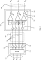
- FIG. 3 is a block diagram of an ODVS communications system, in which a data-aligned strobe signal (comparable to the strobe associated with known LPDDR4 channels) is carried by a sub-channel, and N bits of data are carried on other sub-channels of the same code.
- a collection of multi-input comparators 132 detects the received information, outputting data 345 and a received data-aligned strobe 346.
- Introduction of a one-half unit interval time delay 350 offsets the received strobe to produce an eye-aligned strobe 356 having a transition edge at the optimum sampling time to latch data 345.
- Methods of embodiment for delay 350 as well as any associated adjustment or calibration means it may require is well known in the art for LPDDR interfaces.
- LPDDR4 The existing LPDDR4 specification provides for eight data wires, one wire for DMI, and two Strobe wires, for a total of 11 wires. These legacy connections may be mapped to a new protocol mode, herein called LPDDR5, using ODVS encoding in several ways.
- a first embodiment, herein identified as Glasswing and shown in the block diagram of FIG. 4 adds a new wire to provide a total of 12 wires that are then logically divided into two groups of six wires each.
- Each group of six wires is used to carry an instance of an ODVS code transmitting 5 bits on 6 wires (called the 5b6w code henceforth), thus providing a total of ten sub-channels.
- Eight sub-channels are used to carry eight bits of data, one sub-channel is used to carry a mask bit (conventionally used during DRAM write operations to block individual byte writes), and one sub-channel is used to carry a data-aligned strobe.
- the 5b6w code is balanced, all symbols within any given codeword summing to zero, and is structured such that each codeword contains exactly one +1 and one -1, the remaining codeword symbols being including +1/3 and - 1/3 symbols.
- multiple permutations of a suitable codeword set and corresponding comparator detection coefficients may be used in embodiments.
- Each 5b6w receiver in Glasswing incorporates five multi-input comparators.
- the codewords of each instance of the 5b6w code are shown in Table 1 and the set of comparators are: x 0 ⁇ x 1 x 0 + x 1 / 2 ⁇ x 2 x 4 ⁇ x 5 x 3 ⁇ x 4 + x 5 / 2 x 0 + x 1 + x 2 / 3 ⁇ x 3 + x 4 + x 5 / 3 where the wires of each six wire group are designated as x0, x1...x5.
- a second embodiment, herein identified as “8b9w” and shown in the block diagram of FIG. 5 retains the existing LPDDR4 compliment of 11 data transfer wires.
- Nine wires are used to carry an 8b9w code internally including a 5 wire code herein called the 4.5b5w code and a 4 wire code herein called the 3.5b4w code, which combined provides 288 distinct codeword combinations of which 257 will be used by the encoder.
- 256 of the codewords are used to encode 8 bits of data when the Mask input is false, and one codeword is used to mark a "do not write" condition when the Mask input is true.
- a data-aligned strobe is communicated using legacy means, using the two existing LPDDR4 strobe wires.
- each 4.5b5w receiver incorporates seven multi-input comparators, using the codewords of the 4.5b5w code as given in Table 2 and the set of comparators x 0 ⁇ x 1 x 0 ⁇ x2 x 0 ⁇ x3 x 1 ⁇ x2 x 1 ⁇ x3 x 2 ⁇ x3 x 0 + x 1 + x 2 + x 3 / 4 ⁇ x 4 where the wires of each five wire group are designated as x0, x1...x4.
- the codewords of the 3.5b4w code are given in Table 3.
- Table 3 ⁇ [1,-1,0,0] ⁇ [0,1,-1,0] ⁇ [1,0,-1,0] ⁇ [0,1,0,-1] ⁇ [1,0,0,-1] ⁇ [0,0,1,-1]
- Each 3.5b4w receiver incorporates six multi-input comparators. If the wires of each four wire group are designated as x0, x1...x3, the comparators are: x 0 ⁇ x1 x 0 ⁇ x2 x 0 ⁇ x3 x 1 ⁇ x2 x 1 ⁇ x 3 x 2 ⁇ x 3
- a third embodiment herein identified as "ENRZ" and shown in the block diagram of FIG. 6 , adds a new wire to the existing LPDDR4 compliment to provide a total of 12 wires that are then logically divided into three groups of four wires each. Each group of four wires is used to carry an instance of ENRZ code, each instance thus having eight unique codewords.
- there is no designated repeat codeword there is no designated repeat codeword.
- the transmitter may store the last transmitted codeword, and produce for the following UI a codeword that is different from the transmitted one, as taught in [Shokrollahi III].
- the Data-aligned strobe is used to clock codeword emission at the transmitter, with the repeat code being emitted on each instance whenever the present codeword to be emitted is identical to the codeword emitted in the previous unit interval.
- a known art clock recover circuit extracts timing information from received codeword edges, and a one data value history buffer regenerates duplicated data values for each instance on detection of a received repeat codeword.
- FIGs. 7A , 7B , and 7C provide a comparison of the various embodiments; with receive eye diagrams shown for Glasswing, ENRZ, and 8b9w embodiments, respectively at signaling rates of 6.4 GBaud and 8.4 GBaud.
- a method 800 comprises receiving, at step 802, a set of symbols of a codeword of a vector signaling code at a plurality of multi-input comparators (MICs), the set of symbols representing a transformation of an input vector with a non-simple orthogonal or unitary matrix, the input vector comprising a plurality of sub-channels, wherein at least one sub-channel corresponds to an input data signal and wherein at least one sub-channel corresponds to a data-aligned strobe signal, forming, at step 802 a set of MIC output signals based on a plurality of comparisons between a plurality of subsets of symbols of the codeword, wherein for each comparison, each subset of symbols has a set of input coefficients applied to it determined by a corresponding MIC, and wherein the set of MIC output signals comprises at least one data output signal and at least one received data-aligned strobe signal, and sampling, at step 806, the at least one data output signal according to the at least one received data
Description
- This application claims priority to
U.S. Provisional Patent Application 62/032,175, filed Aug. 1, 2014 - The following references are discussed in this application:
-
U.S. Patent Publication No. 2011/0268225 ofU.S. patent application Ser. No. 12/784,414, filed May 20, 2010 -
U.S. patent application Ser. No. 13/030,027, filed Feb. 17, 2011 , naming Harm Cronie, Amin Shokrollahi and Armin Tajalli, entitled "Methods and Systems for Noise Resilient, Pin-Efficient and Low Power Communications with Sparse Signaling Codes", hereinafter identified as [Cronie II]; -
U.S. patent application Ser. No. 14/158,452, filed Jan. 17, 2014 -
U.S. patent application Ser. No. 13/842,740, filed Mar. 15, 2013 -
U.S. Provisional Patent Application No. 61/934,804, filed Feb. 2, 2014 -
U.S. Provisional Patent Application No. 61/934,807, filed Feb. 2, 2014 -
U.S. Provisional Patent Application No. 61/839,360, filed Jun. 23, 2013 -
U.S. Provisional Patent Application No. 61/946,574, filed Feb. 28, 2014 -
U.S. Provisional Patent Application No. 62/015,172, filed Jul. 10, 2014 -
U.S. patent application Ser. No. 13/895,206, filed May 15, 2013 -
U.S. Provisional Patent Application No. 62/026,860, filed Jul. 21, 2014 - The following additional references to prior art have been cited in this application:
-
U.S. Pat. No. 7,053,802, filed Apr. 22, 2004 and issued May 30, 2006, naming William Cornelius, entitled "Single-Ended Balance-Coded Interface with Embedded-Timing", hereinafter identified as [Cornelius]; -
U.S. Pat. No. 8,064,535, filed Mar. 2, 2007 and issued Nov. 22, 2011, naming George Wiley, entitled "Three Phase and Polarity Encoded Serial Interface, hereinafter identified as [Wiley]. -
U.S. Pat. No. 8,649,460, filed Mar. 11, 2010 and issued Feb. 11, 2014, naming Frederick Ware and Jade Kizer, entitled "Techniques for Multi-Wire Encoding with an Embedded Clock", hereinafter identified as [Ware]. -
US-A-2002/0174373 discloses a conventional data transmission system using a pair of complementary signals as an edge-aligned strobe signal and input/output buffers therein. - In communication systems, a goal is to transport information from one physical location to another. It is typically desirable that the transport of this information is reliable, is fast and consumes a minimal amount of resources. One common information transfer medium is the serial communications link, which may be based on a single wire circuit relative to ground or other common reference, or multiple such circuits relative to ground or other common reference. A common example uses singled-ended signaling ("SES"). SES operates by sending a signal on one wire, and measuring the signal relative to a fixed reference at the receiver. A serial communication link may also be based on multiple circuits used in relation to each other. A common example of the latter uses differential signaling ("DS"). Differential signaling operates by sending a signal on one wire and the opposite of that signal on a matching wire. The signal information is represented by the difference between the wires, rather than their absolute values relative to ground or other fixed reference.
- There are a number of signaling methods that maintain the desirable properties of DS while increasing pin efficiency over DS. Vector signaling is a method of signaling. With vector signaling, a plurality of signals on a plurality of wires is considered collectively although each of the plurality of signals might be independent. Each of the collective signals is referred to as a component and the number of plurality of wires is referred to as the "dimension" of the vector. In some embodiments, the signal on one wire is entirely dependent on the signal on another wire, as is the case with DS pairs, so in some cases the dimension of the vector might refer to the number of degrees of freedom of signals on the plurality of wires instead of exactly the number of wires in the plurality of wires.
- Any suitable subset of a vector signaling code denotes a "sub code" of that code. Such a subcode may itself be a vector signaling code. With binary vector signaling, each component or "symbol" of the vector takes on one of two possible values. With non-binary vector signaling, each symbol has a value that is a selection from a set of more than two possible values. When transmitted as physical signals on a communications medium, symbols may be represented by particular physical values appropriate to that medium; as examples, in one embodiment a voltage of 150 mV may represent a "+1" symbol and a voltage of 50 mV may represent a "-1" symbol, while in another embodiment "+1" may be represented by 800 mV and "-1" as -800 mV.
- A vector signaling code, as described herein, is a collection C of vectors of the same length N, called codewords. The ratio between the binary logarithm of the size of C and the length N is called the pin-efficiency of the vector signaling code. The Orthogonal Differential Vector Signaling codes of [Cronie I], [Cronie II], [Fox I], [Shokrollahi I], [Shokrollahi II], and [Shokrollahi III] are examples of vector signaling codes, and are used herein for descriptive purposes.
-
FIG. 1 illustrates a communication system employing vector signaling codes. Bits S0, S1, S2 enterblock-wise 100 into an encoder 105. The size of the block may vary and depends on the parameters of the vector signaling code. The encoder generates a codeword of the vector signaling code for which the system is designed. In operation, the encoder may generate information used to control PMOS and NMOS transistors withindriver 110, generating voltages or currents on theN communication wires 125 comprising thecommunications channel 120.Receiver 132 reads the signals on the wires, possibly including amplification, frequency compensation, and common mode signal cancellation.Receiver 132 provides its results todecoder 138, which recreates the input bits at 140, here shown as received bits R0, R1, R2. - Depending on which vector signaling code is used, there may be no decoder, or no encoder, or neither a decoder nor an encoder. For example, for the 8b8w code disclosed in [Cronie II], both
encoder 112 and decoder 1138 exist. On the other hand, for the Hadamard code disclosed in [Cronie I], an explicit decoder may be unnecessary, as the system may be configured such thatreceiver 132 generatesoutput bits 140 directly. - The operation of the
transmitting device 110, comprisinginput data 100 andelements receiving device 130, includingelement 132,optional element 138, andoutput data 140, have to be completely synchronized in order to guarantee correct functioning of the communication system. In some embodiments, this synchronization is performed by an external clock shared between the transmitter and the receiver. Other embodiments may combine the clock function with one or more of the data channels, as in the well-known Biphase encoding used for serial communications. - One important example is provided by memory interfaces in which a clock is generated on the controller and shared with the memory device. The memory device may use the clock information for its internal memory operations, as well as for I/O. Because of the burstiness and the asynchronicity of memory operations, the I/O may not be active all the time. Moreover, the main clock and the data lines may not be aligned due to skew. In such cases, additional strobe signals are used to indicate when to read and write the data.
- According to one aspect of the present invention, there is provided a method as defined in
claim 1 hereinafter. - According to another aspect of the present invention, there is provided an apparatus as defined in
claim 9 hereinafter. - The embodiment disclosed with respect to
Figure 5 does not fall under the scope of the claims. - Orthogonal differential vector signaling codes providing transport for both data and a clocking signal are described which are suitable for implementation in both conventional high-speed CMOS and DRAM integrated circuit processes. Example channels derived from current practice for Low-Powered DDR4 interfaces are described, as are modest channel enhancements providing higher speed and greater signal integrity.
-
-
FIG. 1 illustrates a communication system employing vector signaling codes. -
FIG. 2 illustrates one embodiment of an ODVS communications system in which a discrete decoding function is not required. -
FIG. 3 is a block diagram of an embodiment transporting data and a clock signal using ODVS code, and incorporating elements facilitating integration of the receiver with conventional DRAM practice. -
FIG. 4 is a block diagram of an embodiment utilizing 5b6w code, also known as Glasswing, to implement transport over a proposed LPDDR5 channel. -
FIG. 5 is a block diagram of an embodiment utilizing 8b9w code to implement transport over a proposed LPDDR5 channel. -
FIG. 6 is a block diagram of an embodiment utilizing ENRZ code to implement transport over a proposed LPDDR5 channel. -
FIGs. 7A ,7B , and7C shows comparative receive eye diagrams for Glasswing, ENRZ, and 8b9w embodiments, respectively, operating at 6.4 GBaud and 8.4 GBaud signaling rates. -
FIG. 8 depicts a process in accordance with at least one embodiment. -
FIG. 1 illustrates a communication system employing vector signaling codes. Source data totransmitter 110, herein illustrated as S0, S1, S2 enter block-wise 100 intoencoder 112. The size of the block may vary and depends on the parameters of the vector signaling code. Theencoder 112 generates a codeword of the vector signaling code for which the system is designed. In operation, the codeword produced byencoder 112 is used to control PMOS and NMOS transistors withindriver 118, generating two, three, or more distinct voltages or currents on each of theN communication wires 125 ofcommunications channel 120, to represent the N symbols of the codeword. Withincommunications receiver 130,receiver 132 reads the voltages or currents on theN wires 125, possibly including amplification, frequency compensation, and common mode signal cancellation, providing its results todecoder 138, which recreates the input bits as receivedresults 140, herein shown as R0, R1, R2. As will be readily apparent, different codes may be associated with different block sizes and different codeword sizes; for descriptive convenience and without implying limitation, the example ofFIG. 1 illustrates a system using an ODVS code capable of encoding a three binary bit value for transmission over four wires, a so-called 3b4w code. - Depending on which vector signaling code is used, there may be no decoder, or no encoder, or neither a decoder nor an encoder. For example, for the 8b8w code disclosed in [Cronie II], both
encoder 112 anddecoder 138 exist. On the other hand, for the H4 code disclosed in [Cronie I] (also described herein as ENRZ,) an explicit decoder may be unnecessary, as the system may be configured such thatreceiver 132 generates the receivedresults 140 directly. - The operation of the
communications transmitter 110 andcommunications receiver 130 have to be completely synchronized in order to guarantee correct functioning of the communication system. In some embodiments, this synchronization is performed by an external clock shared between the transmitter and the receiver. Other embodiments may combine the clock function with one or more of the data channels, as in the well-known Biphase encoding used for serial communications. - One important example is provided by memory interfaces in which a clock is generated on the controller and shared with the memory device. The memory device may use the clock information for its internal memory operations, as well as for I/O. Because of the burstiness and the asynchronicity of memory operations, the I/O may not be active all the time. Moreover, the main clock and the data lines may not be aligned due to skew. In such cases, additional strobe signals are used to indicate when to read and write the data.
- The interface between a system memory controller and multiple Dynamic RAM devices has been well optimized over multiple design generations for both transfer speed and low power consumption. The present state of the art DRAM interface, LPDDR4, includes 8 data lines, 1 DMI signal, 2 strobe lines, as well as other non-data-transfer related lines.
- There is considerable interest in extending LPDDR4 to support higher performance at equal or less power consumption, but simple performance extrapolations of the existing technology seem problematic. Decreasing signal integrity precludes simply raising data transfer rates using the existing single-ended interconnection, and misalignment of received DRAM data and its strobe signal is a known issue even at current clock speeds. However, introduction of new technology is constrained by a strong desire to retain as much of the conventional practice as possible regarding bus layout, signal distribution, clocking, etc., as well as a hard requirement that the new technology be implementable in both the high-speed CMOS process used for memory controllers, and in the highly specialized DRAM fabrication process which produces extremely small, high capacitance and low leakage memory cells, but comparatively slow digital and interface logic.
- Because of this slow logic speed, conventional DRAM designs utilize two or more phases of processing logic to handle the current LPDDR4 data transfer rates, as one example using one phase of processing logic to capture data on the rising edge of the data transfer strobe, and another phase of processing logic to capture data on the falling edge of the strobe. One hidden limitation of such multi-phased processing embodiments is the difficulty of extracting difference-based information from consecutively received unit intervals, as consecutive unit intervals by definition are known only by different processing phases. Thus, multi-phased processing is problematic for both codes using transition-encoding, as well as embedded- or self-clocking data solutions that rely on comparison of data values received in consecutive unit intervals.
- These issues of clock extraction, and transition- or change-detection are most intractable in the communications receiver embodiment, thus the examples herein focus on embodiments in which the relatively slow DRAM device is the receiver. No limitation is implied, as one familiar with the art will readily acknowledge that bidirectional data communication with DRAM devices is well understood, and that any example embodiment suitable for DRAM receive implementation could easily implement the simpler transmit requirements as well.
- As described in [Holden I], a multi-input comparator with coefficients a 0, a 1, ...,a m-1, is a circuit that accepts as its input a vector (x 0, x 1, ..,x m-1) and outputs

- In many embodiments, the desired output is a binary value, thus the value Result is sliced with an analog comparator to produce a binary decision output. Because this is a common use, the colloquial name of this circuit incorporates the term "comparator", although other embodiments may use a PAM-3 or PAM-4 slicer to obtain ternary or quaternary outputs, or indeed may retain the analog output of Eqn. 1 for further computation. In at least one embodiment, the coefficients are selected according to sub-channel vectors corresponding to rows of a non-simple orthogonal or unitary matrix used to generate the ODVS code.
- As one example, [Ulrich I] teaches that the ODVS code herein called ENRZ may be detected using three instances of the same four input multi-input comparator, performing the
operations 


- It is conventional to consider the data input to encoder 112 of
FIG. 1 as vectors of data (i.e., a data word) to be atomically encoded as a codeword to be transmitted acrosschannel 120, detected byreceiver 132, and ultimately decoded 138 to produce a received reconstruction of the transmitted vector or data word. - However, it is equally accurate to model the communications system in a somewhat different way. As this alternate model is most easily understood in a system not requiring a separate decoder, a particular embodiment based on the ENRZ code as illustrated in
FIG. 2 will be used for purposes of description, with no limitation being implied. Elements inFIG. 2 functionally identical to elements ofFIG. 1 are identically numbered, althoughFIG. 2 may subsequently illustrate additional internal structure or composition of features that are generically described inFIG. 1 - In
FIG. 2 ,input data vector 100entering communications transmitter 110 is explicitly shown to be expanded to its individual bits S0, S1, S2 and enteringencoder 112. Individual signals representing the symbols of the codeword output byencoder 112 are shown controllingindividual line drivers 118 to emit signals ontowires 125 comprisingcommunications channel 120. As any one wire transporting the ENRZ code can take on one of four different signal values, two control signals are shown controlling each wire's line driver. - As previously noted, in this
embodiment communications receiver 130 does not require an explicit decoder. The internal structure ofreceiver 132 is illustrated, comprising four receive front ends (as 131) that accept signals fromwires 125, and optionally may include amplification and equalization, as required by the characteristics of thecommunications channel 120. Three multi-input comparators are shown with their inputs connected to the four received wire signals as described by Eqns. 2, 3, and 4. For avoidance of confusion, the multi-input comparators are illustrated as including acomputational function 133 followed by aslicing function 134 producing digital outputs R0, R1, R2 from the computational combination of the input values. - One familiar with the art may note that the ODVS encoder accepts one set of input data and outputs one codeword per transmit unit interval. If, as is the case in many embodiments, the encoder includes combinatorial digital logic (i.e. without additional internal state,) this periodic codeword output may easily be seen as performing a sampling function on the input data followed by the encoding transformation, subsequent transmission, etc. Similarly, if the detection operation within the receiver is similarly combinatorial, as is the case here with multi-input comparators performing the detection, the state of a given output element is solely determined by the received signal levels on some number of channel wires. Thus, each independent signal input (as one example, S0) and its equivalent independent signal output (as R0) may be considered a virtual communications channel, herein called a "sub-channel" of the ODVS encoded system. A given sub-channel may be binary (i.e. communicate a two-state value) or may represent a higher-ordered value. Indeed, as taught by [Shokrollahi IV], the sub-channels of a given ODVS code are sufficiently independent that they may utilize different alphabets (and sizes of alphabets) to describe the values they communicate.
- All data communications in an ODVS system, including the state changes in sub-channels, are communicated as codewords over the entire channel. An embodiment may associate particular mappings of input values to codewords and correlate those mappings with particular detector results, as taught by [Holden I] and [Ulrich I], but those correlations should not be confused with partitions, sub-divisions, or sub-channels of the communications medium itself.
- The concept of ODVS sub-channels is not limited by the example embodiment to a particular ODVS code, transmitter embodiment, or receiver embodiment. Encoders and/or decoders maintaining internal state may also be components of embodiments. Sub-channels may be represented by individual signals, or by states communicated by multiple signals.
- As an ODVS communications system must communicate each combination of data inputs as encoded transmissions, and the rate of such encoded transmissions is of necessity constrained by the capacity of the communications medium, the rate of change of the data to be transmitted must be within the Nyquist limit, where the rate of transmission of codewords represents the sampling interval. As one example, a binary clock or strobe signal may be transmitted on an ODVS sub-channel, if it has no more than one clock edge per codeword transmission.
- An embodiment of an ODVS encoder and its associated line drivers may operate asynchronously, responding to any changes in data inputs. Other embodiments utilize internal timing clocks to, as one example, combine multiple phases of data processing to produce a single high-speed output stream. In such embodiments, output of all elements of a codeword is inherently simultaneous, thus a strobe or clock signal being transported on a sub-channel of the code will be seen at the receiver as a data-aligned clock (e.g. with its transition edges occurring simultaneous to data edges on other sub-channels of the same code.) Similar timing relationships are often presumed in clock-less or asynchronous embodiments as well.
-
FIG. 3 is a block diagram of an ODVS communications system, in which a data-aligned strobe signal (comparable to the strobe associated with known LPDDR4 channels) is carried by a sub-channel, and N bits of data are carried on other sub-channels of the same code. At the receiver, a collection ofmulti-input comparators 132 detects the received information, outputtingdata 345 and a received data-alignedstrobe 346. Introduction of a one-half unitinterval time delay 350 offsets the received strobe to produce an eye-alignedstrobe 356 having a transition edge at the optimum sampling time to latchdata 345. As is conventional in many DRAM embodiments, two processing phases are shown for data sampling;phase 360sampling data 345 on the negative edge of eye-alignedstrobe 356, andphase 370sampling data 345 on the positive edge of eye-alignedstrobe 356. Methods of embodiment fordelay 350 as well as any associated adjustment or calibration means it may require is well known in the art for LPDDR interfaces. - The existing LPDDR4 specification provides for eight data wires, one wire for DMI, and two Strobe wires, for a total of 11 wires. These legacy connections may be mapped to a new protocol mode, herein called LPDDR5, using ODVS encoding in several ways.
- As taught by [Holden I], the noise characteristics of a multi-input comparator are dependent on its input size and configuration. [Shokrollahi IV] also teaches that the signal amplitudes resulting from various computations as Eqn. 1 can present different receive eye characteristics. Thus, preferred embodiments will designate a higher quality (e.g. wider eye opening) sub-channel to carry clock, strobe, or other timing information, when the characteristics of the available sub-channels vary.
- A first embodiment, herein identified as Glasswing and shown in the block diagram of
FIG. 4 , adds a new wire to provide a total of 12 wires that are then logically divided into two groups of six wires each. Each group of six wires is used to carry an instance of an ODVS code transmitting 5 bits on 6 wires (called the 5b6w code henceforth), thus providing a total of ten sub-channels. Eight sub-channels are used to carry eight bits of data, one sub-channel is used to carry a mask bit (conventionally used during DRAM write operations to block individual byte writes), and one sub-channel is used to carry a data-aligned strobe. The 5b6w code is balanced, all symbols within any given codeword summing to zero, and is structured such that each codeword contains exactly one +1 and one -1, the remaining codeword symbols being including +1/3 and - 1/3 symbols. As will be apparent to one familiar with the art, multiple permutations of a suitable codeword set and corresponding comparator detection coefficients may be used in embodiments. - Each 5b6w receiver in Glasswing incorporates five multi-input comparators. In a preferred embodiment, the codewords of each instance of the 5b6w code are shown in Table 1 and the set of comparators are:


Table 1 ± [1, 1/3, -1/3, -1, -1/3, 1/3] ± [1, 1/3, -1/3, 1/3, -1, -1/3] ± [1/3, 1, -1/3, -1, -1/3, 1/3] ± [1/3, 1, -1/3, 1/3, -1, -1/3] ± [1/3, -1/3, 1, -1, -1/3, 1/3] ± [1/3, -1/3, 1, 1/3, -1, -1/3] ± [-1/3, 1/3, 1, -1, -1/3, 1/3] ± [-1/3, 1/3, 1, 1/3, -1, -1/3] ± [1, 1/3, -1/3, -1, 1/3, -1/3] ± [1, 1/3, -1/3, 1/3, -1/3, -1] ± [1/3, 1, -1/3, -1, 1/3, -1/3] ± [1/3, 1, -1/3, 1/3, -1/3, -1] ± [1/3, -1/3, 1, -1, 1/3, -1/3] ± [1/3, -1/3, 1, 1/3, -1/3, -1] ± [-1/3, 1/3, 1, -1, 1/3, -1/3] ± [-1/3, 1/3, 1, 1/3, -1/3, -1] - Additional information about this 5b6w code is provided in [Ulrich II].
- A second embodiment, herein identified as "8b9w" and shown in the block diagram of
FIG. 5 , retains the existing LPDDR4 compliment of 11 data transfer wires. Nine wires are used to carry an 8b9w code internally including a 5 wire code herein called the 4.5b5w code and a 4 wire code herein called the 3.5b4w code, which combined provides 288 distinct codeword combinations of which 257 will be used by the encoder. 256 of the codewords are used to encode 8 bits of data when the Mask input is false, and one codeword is used to mark a "do not write" condition when the Mask input is true. A data-aligned strobe is communicated using legacy means, using the two existing LPDDR4 strobe wires. - In at least one embodiment, each 4.5b5w receiver incorporates seven multi-input comparators, using the codewords of the 4.5b5w code as given in Table 2 and the set of comparators


Table 2 ± [0,-1,1,1,-1] ± [-1,1,0,1,-1] ± [0,1,-1,1,-1] ± [1,-1,0,1,-1] ± [0,1,1,-1,-1] ± [1,1,0,-1,-1] ± [-1,0,1,1,-1] ± [-1,1,1,0,-1] ± [1,0,-1,1,-1] ± [1,-1,1,0,-1] ± [1,0,1,-1,-1] ± [1,1,-1,0,-1] - The ISI-ratio of the first 6 comparators (as defined in [Hormati I]) is 2, whereas the ISI-ratio of the last comparator is 1.
- In the same embodiments, the codewords of the 3.5b4w code are given in Table 3.
Table 3 ± [1,-1,0,0] ± [0,1,-1,0] ± [1,0,-1,0] ± [0,1,0,-1] ± [1,0,0,-1] ± [0,0,1,-1] - Each 3.5b4w receiver incorporates six multi-input comparators. If the wires of each four wire group are designated as x0, x1...x3, the comparators are:


- The ISI-ratio of all these comparators (as defined in [Hormati I]) is 2.
- A third embodiment, herein identified as "ENRZ" and shown in the block diagram of
FIG. 6 , adds a new wire to the existing LPDDR4 compliment to provide a total of 12 wires that are then logically divided into three groups of four wires each. Each group of four wires is used to carry an instance of ENRZ code, each instance thus having eight unique codewords. In at least one embodiment, one codeword from each instance is reserved as a repeat code, with the seven remaining codewords per instance being combined by the encoder to provide 7 ∗ 7 ∗ 7 = 343 unique combinations, more than sufficient to encode eight data bits and a mask condition, as in the previous example. In another embodiment, there is no designated repeat codeword. Instead, the transmitter may store the last transmitted codeword, and produce for the following UI a codeword that is different from the transmitted one, as taught in [Shokrollahi III]. The Data-aligned strobe is used to clock codeword emission at the transmitter, with the repeat code being emitted on each instance whenever the present codeword to be emitted is identical to the codeword emitted in the previous unit interval. At the receiver, a known art clock recover circuit extracts timing information from received codeword edges, and a one data value history buffer regenerates duplicated data values for each instance on detection of a received repeat codeword. - Further description of this embodiment may be found in [Shokrollahi III].
-
FIGs. 7A ,7B , and7C provide a comparison of the various embodiments; with receive eye diagrams shown for Glasswing, ENRZ, and 8b9w embodiments, respectively at signaling rates of 6.4 GBaud and 8.4 GBaud. - The examples presented herein illustrate the use of vector signaling codes for point-to-point wire communications. However, this should not been seen in any way as limiting the scope of the described embodiments. The methods disclosed in this application are equally applicable to other communication media including optical and wireless communications. Thus, descriptive terms such as "voltage" or "signal level" should be considered to include equivalents in other measurement systems, such as "optical intensity", "RF modulation", etc. As used herein, the term "physical signal" includes any suitable behavior and/or attribute of a physical phenomenon capable of conveying information. Physical signals may be tangible and non-transitory.
- In
Figure 8 amethod 800 comprises receiving, atstep 802, a set of symbols of a codeword of a vector signaling code at a plurality of multi-input comparators (MICs), the set of symbols representing a transformation of an input vector with a non-simple orthogonal or unitary matrix, the input vector comprising a plurality of sub-channels, wherein at least one sub-channel corresponds to an input data signal and wherein at least one sub-channel corresponds to a data-aligned strobe signal, forming, at step 802 a set of MIC output signals based on a plurality of comparisons between a plurality of subsets of symbols of the codeword, wherein for each comparison, each subset of symbols has a set of input coefficients applied to it determined by a corresponding MIC, and wherein the set of MIC output signals comprises at least one data output signal and at least one received data-aligned strobe signal, and sampling, atstep 806, the at least one data output signal according to the at least one received data-aligned strobe signal.
Claims (15)
- A method comprising:receiving (802), at a plurality of multi-input comparators (133) via a multi-wire bus, a set of symbols of a codeword of a balanced vector signaling code, each symbol of the set of symbols received by at least two multi-input comparators, all symbols within any given codeword summing to zero, the set of symbols representing a transformation of an input vector with a plurality of sub-channel vectors corresponding to rows of a non-simple orthogonal or unitary matrix, the input vector comprising a plurality of sub-channels, wherein (i) at least one sub-channel corresponds to an input data signal carried by a corresponding data sub-channel vector and (ii) wherein at least one sub-channel corresponds to a data-aligned strobe signal carried by a data-aligned strobe sub-channel vector orthogonal to the corresponding data sub-channel vectors;forming (804) a set of multi-input comparator output signals, each multi-input comparator output signal generated based on a computational combination of a respective subset of symbols of the codeword, the respective subset of symbols having a respective set of input coefficients of a plurality of sets of input coefficients applied to it by a corresponding multi-input comparator (133), the respective subset of symbols of the codeword and the respective set of input coefficients of the computational combination selected according to a corresponding sub-channel vector of the plurality of sub-channel vectors, and wherein the set of multi-input comparator output signals comprises at least one data output signal and a received data-aligned strobe signal, the received data-aligned strobe signal generated using a multi-input comparator of the plurality of multi-input comparators operating on symbols of the codeword each of which are a weighted sum of corresponding elements of the data-aligned strobe sub-channel vector and corresponding elements of one or more of the corresponding data sub-channel vectors; and,sampling (806) the at least one data output signal according to the received data-aligned strobe signal.
- The method of claim 1, wherein at least one data output signal is sampled on a rising edge of the received data-aligned strobe signal.
- The method of claim 1, wherein at least one output data signal is sampled on a falling edge of the received data-aligned strobe signal.
- The method of claim 1, wherein the input vector comprises 4 sub-channels corresponding to input data signals and 1 sub-channel corresponding to the received data-aligned strobe signal.
- The method of claim 4, wherein each symbol of the set of symbols has a value selected from the set of values {+1, +1/3, -1/3, -1}.
- The method of claim 5, wherein the vector signaling code comprises the codewords:± [1, 1/3, -1/3, -1, -1/3, 1/3]± [1/3, 1, -1/3, -1, -1/3, 1/3]± [1/3, -1/3, 1, -1, -1/3, 1/3]± [-1/3, 1/3, 1, -1, -1/3, 1/3]± [1, 1/3, -1/3, -1, 1/3, -1/3]± [1/3, 1, -1/3, -1, 1/3, -1/3]± [1/3, -1/3, 1, -1, 1/3, -1/3]± [-1/3, 1/3, 1, -1, 1/3, -1/3]± [1, 1/3, -1/3, 1/3, -1, -1/3]± [1/3, 1, -1/3, 1/3, -1, -1/3]± [1/3, -1/3, 1, 1/3, -1, -1/3]± [-1/3, 1/3, 1, 1/3, -1, -1/3]± [1, 1/3, -1/3, 1/3, -1/3, -1]± [1/3, 1, -1/3, 1/3, -1/3, -1]± [1/3, -1/3, 1, 1/3, -1/3, -1]± [-1/3, 1/3, 1, 1/3, -1/3, -1].
- The method of claim 1, further comprising forming a set of output bits by slicing the set of multi-input comparator output signals.
- The method of claim 1, further comprising:receiving the input vector on a plurality of wires (100);generating, using an encoder (112), the set of symbols of the codeword representing a weighted sum of sub-channel vectors, the sub-channel vectors corresponding to rows of the non-simple orthogonal or unitary matrix, wherein a weighting of each sub-channel vector is determined by a corresponding input vector sub-channel; and,providing the symbols of the codeword on a multi-wire bus.
- An apparatus comprising:a multi-wire bus configured to provide a set of symbols of a codeword of a balanced vector signaling code to a plurality of multi-input comparators (133), each symbol of the set of symbols provided to at least two multi-input comparators, all symbols within any given codeword summing to zero, the set of symbols representing a transformation of an input vector with a plurality of sub-channel vectors corresponding to rows of a non-simple orthogonal or unitary matrix, the input vector comprising a plurality of sub-channels, wherein (i) at least one sub-channel corresponds to an input data signal carried by corresponding data sub-channel vectors and (ii) wherein at least one sub-channel corresponds to a data-aligned strobe signal, carried by a data-aligned strobe sub-channel vector orthogonal to the corresponding data sub-channel vectors;the plurality of multi-input comparators (133) configured to form a set of multi-input comparator output signals, each multi-input comparator output signal generated based on a computational combination of a plurality of subsets respective subset of symbols of the codeword, respective subset of symbols having a respective set of input coefficients of a plurality of sets of input coefficients applied to it by a corresponding multi-input comparator (133), the respective subset of symbols of the codeword and the respective set of input coefficients of the computational combination selected according to a corresponding sub-channel vector of the plurality of sub-channel vectors, and wherein the set of multi-input comparator output signals comprises at least one data output signal and a received data-aligned strobe signal, the received data-aligned strobe signal generated using a multi-input comparator of the plurality of multi-input comparators operating on symbols of the codeword each of which are a weighted sum of corresponding elements of the data-aligned strobe sub-channel vector and corresponding elements of one or more of the corresponding data sub-channel vectors; and,a plurality of sampling circuits configured to sample the at least one data output signal according to the received data-aligned strobe signal.
- The apparatus of claim 9, wherein at least one sampling circuit is configured to sample at least one data output signal on a rising edge of the received data-aligned strobe signal.
- The apparatus of claim 9, wherein at least one sampling circuit is configured to sample at least one output data signal on a falling edge of the received data-aligned strobe signal.
- The apparatus of claim 9, wherein the input vector comprises 4 sub-channels corresponding to input data signals and 1 sub-channel corresponding to the received data-aligned strobe signal.
- The apparatus of claim 9, wherein each symbol of the set of symbols has a value selected from the set of values {+1, +1/3, -1/3, -1}.
- The apparatus of claim 13, wherein the vector signaling code comprises the codewords:± [1, 1/3, -1/3, -1, -1/3, 1/3]± [1/3, 1, -1/3, -1, -1/3, 1/3]± [1/3, -1/3, 1, -1, -1/3, 1/3]± [-1/3, 1/3, 1, -1, -1/3, 1/3]± [1, 1/3, -1/3, -1, 1/3, -1/3]± [1/3, 1, -1/3, -1, 1/3, -1/3]± [1/3, -1/3, 1, -1, 1/3, -1/3]± [-1/3, 1/3, 1, -1, 1/3, -1/3]± [1, 1/3, -1/3, 1/3, -1, -1/3]± [1/3, 1, -1/3, 1/3, -1, -1/3]± [1/3, -1/3, 1, 1/3, -1, -1/3]± [-1/3, 1/3, 1, 1/3, -1, -1/3]± [1, 1/3, -1/3, 1/3, -1/3, -1]± [1/3, 1, -1/3, 1/3, -1/3, -1]± [1/3, -1/3, 1, 1/3, -1/3, -1]± [-1/3, 1/3, 1, 1/3, -1/3, -1].
- The apparatus of claim 9, further comprising a plurality of slicers configured to generate a set of output bits by slicing the plurality of multi-input comparator output signals.
Applications Claiming Priority (2)
| Application Number | Priority Date | Filing Date | Title |
|---|---|---|---|
| US201462032175P | 2014-08-01 | 2014-08-01 | |
| PCT/US2015/043463 WO2016019384A1 (en) | 2014-08-01 | 2015-08-03 | Orthogonal differential vector signaling codes with embedded clock |
Publications (3)
| Publication Number | Publication Date |
|---|---|
| EP3175592A1 EP3175592A1 (en) | 2017-06-07 |
| EP3175592A4 EP3175592A4 (en) | 2018-01-17 |
| EP3175592B1 true EP3175592B1 (en) | 2021-12-29 |
Family
ID=55181167
Family Applications (1)
| Application Number | Title | Priority Date | Filing Date |
|---|---|---|---|
| EP15827077.7A Active EP3175592B1 (en) | 2014-08-01 | 2015-08-03 | Orthogonal differential vector signaling codes with embedded clock |
Country Status (5)
| Country | Link |
|---|---|
| US (4) | US9461862B2 (en) |
| EP (1) | EP3175592B1 (en) |
| KR (1) | KR101949964B1 (en) |
| CN (2) | CN106576087B (en) |
| WO (1) | WO2016019384A1 (en) |
Families Citing this family (68)
| Publication number | Priority date | Publication date | Assignee | Title |
|---|---|---|---|---|
| US9288089B2 (en) | 2010-04-30 | 2016-03-15 | Ecole Polytechnique Federale De Lausanne (Epfl) | Orthogonal differential vector signaling |
| US9246713B2 (en) | 2010-05-20 | 2016-01-26 | Kandou Labs, S.A. | Vector signaling with reduced receiver complexity |
| US9564994B2 (en) | 2010-05-20 | 2017-02-07 | Kandou Labs, S.A. | Fault tolerant chip-to-chip communication with advanced voltage |
| US9106220B2 (en) | 2010-05-20 | 2015-08-11 | Kandou Labs, S.A. | Methods and systems for high bandwidth chip-to-chip communications interface |
| US9985634B2 (en) | 2010-05-20 | 2018-05-29 | Kandou Labs, S.A. | Data-driven voltage regulator |
| US9596109B2 (en) | 2010-05-20 | 2017-03-14 | Kandou Labs, S.A. | Methods and systems for high bandwidth communications interface |
| US8593305B1 (en) | 2011-07-05 | 2013-11-26 | Kandou Labs, S.A. | Efficient processing and detection of balanced codes |
| US9479369B1 (en) | 2010-05-20 | 2016-10-25 | Kandou Labs, S.A. | Vector signaling codes with high pin-efficiency for chip-to-chip communication and storage |
| US9450744B2 (en) | 2010-05-20 | 2016-09-20 | Kandou Lab, S.A. | Control loop management and vector signaling code communications links |
| US9077386B1 (en) | 2010-05-20 | 2015-07-07 | Kandou Labs, S.A. | Methods and systems for selection of unions of vector signaling codes for power and pin efficient chip-to-chip communication |
| US9251873B1 (en) | 2010-05-20 | 2016-02-02 | Kandou Labs, S.A. | Methods and systems for pin-efficient memory controller interface using vector signaling codes for chip-to-chip communications |
| US9288082B1 (en) | 2010-05-20 | 2016-03-15 | Kandou Labs, S.A. | Circuits for efficient detection of vector signaling codes for chip-to-chip communication using sums of differences |
| US9667379B2 (en) | 2010-06-04 | 2017-05-30 | Ecole Polytechnique Federale De Lausanne (Epfl) | Error control coding for orthogonal differential vector signaling |
| US9275720B2 (en) | 2010-12-30 | 2016-03-01 | Kandou Labs, S.A. | Differential vector storage for dynamic random access memory |
| US9268683B1 (en) | 2012-05-14 | 2016-02-23 | Kandou Labs, S.A. | Storage method and apparatus for random access memory using codeword storage |
| CN104995612B (en) | 2013-01-17 | 2020-01-03 | 康杜实验室公司 | Inter-chip communication method and system with low synchronous switching noise |
| KR102241045B1 (en) | 2013-04-16 | 2021-04-19 | 칸도우 랩스 에스에이 | Methods and systems for high bandwidth communications interface |
| EP2997704B1 (en) | 2013-06-25 | 2020-12-16 | Kandou Labs S.A. | Vector signaling with reduced receiver complexity |
| US9106465B2 (en) | 2013-11-22 | 2015-08-11 | Kandou Labs, S.A. | Multiwire linear equalizer for vector signaling code receiver |
| US9806761B1 (en) | 2014-01-31 | 2017-10-31 | Kandou Labs, S.A. | Methods and systems for reduction of nearest-neighbor crosstalk |
| WO2015117102A1 (en) | 2014-02-02 | 2015-08-06 | Kandou Labs SA | Method and apparatus for low power chip-to-chip communications with constrained isi ratio |
| EP3111607B1 (en) | 2014-02-28 | 2020-04-08 | Kandou Labs SA | Clock-embedded vector signaling codes |
| US9509437B2 (en) | 2014-05-13 | 2016-11-29 | Kandou Labs, S.A. | Vector signaling code with improved noise margin |
| US11240076B2 (en) | 2014-05-13 | 2022-02-01 | Kandou Labs, S.A. | Vector signaling code with improved noise margin |
| US9148087B1 (en) | 2014-05-16 | 2015-09-29 | Kandou Labs, S.A. | Symmetric is linear equalization circuit with increased gain |
| US9852806B2 (en) | 2014-06-20 | 2017-12-26 | Kandou Labs, S.A. | System for generating a test pattern to detect and isolate stuck faults for an interface using transition coding |
| US9112550B1 (en) | 2014-06-25 | 2015-08-18 | Kandou Labs, SA | Multilevel driver for high speed chip-to-chip communications |
| KR102288337B1 (en) * | 2014-07-10 | 2021-08-11 | 칸도우 랩스 에스에이 | Vector signaling codes with increased signal to noise characteristics |
| US9432082B2 (en) | 2014-07-17 | 2016-08-30 | Kandou Labs, S.A. | Bus reversable orthogonal differential vector signaling codes |
| US9444654B2 (en) | 2014-07-21 | 2016-09-13 | Kandou Labs, S.A. | Multidrop data transfer |
| KR101949964B1 (en) | 2014-08-01 | 2019-02-20 | 칸도우 랩스 에스에이 | Orthogonal differential vector signaling codes with embedded clock |
| US9674014B2 (en) | 2014-10-22 | 2017-06-06 | Kandou Labs, S.A. | Method and apparatus for high speed chip-to-chip communications |
| CN105991507A (en) * | 2015-03-06 | 2016-10-05 | 富士通株式会社 | Data transmission method, data demodulation method, device and system |
| WO2016210445A1 (en) | 2015-06-26 | 2016-12-29 | Kandou Labs, S.A. | High speed communications system |
| US9557760B1 (en) | 2015-10-28 | 2017-01-31 | Kandou Labs, S.A. | Enhanced phase interpolation circuit |
| US9577815B1 (en) | 2015-10-29 | 2017-02-21 | Kandou Labs, S.A. | Clock data alignment system for vector signaling code communications link |
| US10055372B2 (en) * | 2015-11-25 | 2018-08-21 | Kandou Labs, S.A. | Orthogonal differential vector signaling codes with embedded clock |
| EP3408935B1 (en) | 2016-01-25 | 2023-09-27 | Kandou Labs S.A. | Voltage sampler driver with enhanced high-frequency gain |
| US10242749B2 (en) | 2016-04-22 | 2019-03-26 | Kandou Labs, S.A. | Calibration apparatus and method for sampler with adjustable high frequency gain |
| US10003454B2 (en) | 2016-04-22 | 2018-06-19 | Kandou Labs, S.A. | Sampler with low input kickback |
| EP3826184A1 (en) | 2016-04-22 | 2021-05-26 | Kandou Labs, S.A. | High performance phase locked loop |
| US10153591B2 (en) | 2016-04-28 | 2018-12-11 | Kandou Labs, S.A. | Skew-resistant multi-wire channel |
| EP3449606A4 (en) | 2016-04-28 | 2019-11-27 | Kandou Labs S.A. | Low power multilevel driver |
| US10193716B2 (en) | 2016-04-28 | 2019-01-29 | Kandou Labs, S.A. | Clock data recovery with decision feedback equalization |
| CN109313622B (en) * | 2016-04-28 | 2022-04-15 | 康杜实验室公司 | Vector signaling code for dense routing line groups |
| US9906358B1 (en) | 2016-08-31 | 2018-02-27 | Kandou Labs, S.A. | Lock detector for phase lock loop |
| US10411922B2 (en) | 2016-09-16 | 2019-09-10 | Kandou Labs, S.A. | Data-driven phase detector element for phase locked loops |
| US10200188B2 (en) | 2016-10-21 | 2019-02-05 | Kandou Labs, S.A. | Quadrature and duty cycle error correction in matrix phase lock loop |
| US10372665B2 (en) | 2016-10-24 | 2019-08-06 | Kandou Labs, S.A. | Multiphase data receiver with distributed DFE |
| US10200218B2 (en) | 2016-10-24 | 2019-02-05 | Kandou Labs, S.A. | Multi-stage sampler with increased gain |
| CN110741562B (en) | 2017-04-14 | 2022-11-04 | 康杜实验室公司 | Pipelined forward error correction for vector signaling code channels |
| US10693473B2 (en) | 2017-05-22 | 2020-06-23 | Kandou Labs, S.A. | Multi-modal data-driven clock recovery circuit |
| US10116468B1 (en) | 2017-06-28 | 2018-10-30 | Kandou Labs, S.A. | Low power chip-to-chip bidirectional communications |
| US10686583B2 (en) * | 2017-07-04 | 2020-06-16 | Kandou Labs, S.A. | Method for measuring and correcting multi-wire skew |
| US10693587B2 (en) | 2017-07-10 | 2020-06-23 | Kandou Labs, S.A. | Multi-wire permuted forward error correction |
| US10203226B1 (en) | 2017-08-11 | 2019-02-12 | Kandou Labs, S.A. | Phase interpolation circuit |
| US10496583B2 (en) | 2017-09-07 | 2019-12-03 | Kandou Labs, S.A. | Low power multilevel driver for generating wire signals according to summations of a plurality of weighted analog signal components having wire-specific sub-channel weights |
| US10326623B1 (en) | 2017-12-08 | 2019-06-18 | Kandou Labs, S.A. | Methods and systems for providing multi-stage distributed decision feedback equalization |
| US10467177B2 (en) | 2017-12-08 | 2019-11-05 | Kandou Labs, S.A. | High speed memory interface |
| CN111684772B (en) * | 2017-12-28 | 2023-06-16 | 康杜实验室公司 | Synchronous switching multiple-input demodulation comparator |
| US10554380B2 (en) | 2018-01-26 | 2020-02-04 | Kandou Labs, S.A. | Dynamically weighted exclusive or gate having weighted output segments for phase detection and phase interpolation |
| US10243614B1 (en) | 2018-01-26 | 2019-03-26 | Kandou Labs, S.A. | Method and system for calibrating multi-wire skew |
| EP3808044A1 (en) * | 2018-06-12 | 2021-04-21 | Kandou Labs, S.A. | Passive multi-input comparator for orthogonal codes on a multi-wire bus |
| EP3809610B1 (en) * | 2018-07-11 | 2024-03-27 | Huawei Technologies Co., Ltd. | Signal generation device, method, and system |
| KR102223031B1 (en) | 2019-03-20 | 2021-03-04 | 삼성전자주식회사 | Differential signal processing device using for advanced braid clock signaling |
| US10826536B1 (en) | 2019-10-03 | 2020-11-03 | International Business Machines Corporation | Inter-chip data transmission system using single-ended transceivers |
| KR102266069B1 (en) * | 2020-07-09 | 2021-06-18 | 고려대학교 산학협력단 | Wireline transceiver based on pulse amplitude modulation-4 |
| US11831472B1 (en) | 2022-08-30 | 2023-11-28 | Kandou Labs SA | Pre-scaler for orthogonal differential vector signalling |
Family Cites Families (462)
| Publication number | Priority date | Publication date | Assignee | Title |
|---|---|---|---|---|
| US668687A (en) | 1900-12-06 | 1901-02-26 | Louis G Mayer | Thill-coupling. |
| US780883A (en) | 1903-11-18 | 1905-01-24 | Mortimer Livingston Hinchman | Advertising device. |
| US3196351A (en) | 1962-06-26 | 1965-07-20 | Bell Telephone Labor Inc | Permutation code signaling |
| US3636463A (en) | 1969-12-12 | 1972-01-18 | Shell Oil Co | Method of and means for gainranging amplification |
| US3939468A (en) | 1974-01-08 | 1976-02-17 | Whitehall Corporation | Differential charge amplifier for marine seismic applications |
| GB1508986A (en) * | 1974-05-29 | 1978-04-26 | Post Office | Digital network synchronising system |
| US3970795A (en) | 1974-07-16 | 1976-07-20 | The Post Office | Measurement of noise in a communication channel |
| JPS5279747A (en) | 1975-12-26 | 1977-07-05 | Sony Corp | Noise removal circuit |
| US4206316A (en) | 1976-05-24 | 1980-06-03 | Hughes Aircraft Company | Transmitter-receiver system utilizing pulse position modulation and pulse compression |
| US4181967A (en) | 1978-07-18 | 1980-01-01 | Motorola, Inc. | Digital apparatus approximating multiplication of analog signal by sine wave signal and method |
| US4222080A (en) * | 1978-12-21 | 1980-09-09 | International Business Machines Corporation | Velocity tolerant decoding technique |
| US4276543A (en) | 1979-03-19 | 1981-06-30 | Trw Inc. | Monolithic triple diffusion analog to digital converter |
| US4414512A (en) | 1981-05-29 | 1983-11-08 | Motorola Inc. | Broadband peak detector |
| US4486739A (en) | 1982-06-30 | 1984-12-04 | International Business Machines Corporation | Byte oriented DC balanced (0,4) 8B/10B partitioned block transmission code |
| US4499550A (en) | 1982-09-30 | 1985-02-12 | General Electric Company | Walsh function mixer and tone detector |
| US4722084A (en) | 1985-10-02 | 1988-01-26 | Itt Corporation | Array reconfiguration apparatus and methods particularly adapted for use with very large scale integrated circuits |
| US4772845A (en) | 1987-01-15 | 1988-09-20 | Raytheon Company | Cable continuity testor including a sequential state machine |
| US4864303A (en) | 1987-02-13 | 1989-09-05 | Board Of Trustees Of The University Of Illinois | Encoder/decoder system and methodology utilizing conservative coding with block delimiters, for serial communication |
| US4774498A (en) | 1987-03-09 | 1988-09-27 | Tektronix, Inc. | Analog-to-digital converter with error checking and correction circuits |
| US5053974A (en) | 1987-03-31 | 1991-10-01 | Texas Instruments Incorporated | Closeness code and method |
| US4897657A (en) | 1988-06-13 | 1990-01-30 | Integrated Device Technology, Inc. | Analog-to-digital converter having error detection and correction |
| US4974211A (en) | 1989-03-17 | 1990-11-27 | Hewlett-Packard Company | Digital ultrasound system with dynamic focus |
| US5168509A (en) | 1989-04-12 | 1992-12-01 | Kabushiki Kaisha Toshiba | Quadrature amplitude modulation communication system with transparent error correction |
| FR2646741B1 (en) | 1989-05-03 | 1994-09-02 | Thomson Hybrides Microondes | HIGH FREQUENCY SAMPLING SAMPLER-LOCKER |
| US5599550A (en) | 1989-11-18 | 1997-02-04 | Kohlruss; Gregor | Disposable, biodegradable, wax-impregnated dust-cloth |
| US5166956A (en) | 1990-05-21 | 1992-11-24 | North American Philips Corporation | Data transmission system and apparatus providing multi-level differential signal transmission |
| US5150384A (en) | 1990-09-28 | 1992-09-22 | Motorola, Inc. | Carrier recovery method and apparatus having an adjustable response time determined by carrier signal parameters |
| US5266907A (en) | 1991-06-25 | 1993-11-30 | Timeback Fll | Continuously tuneable frequency steerable frequency synthesizer having frequency lock for precision synthesis |
| US5287305A (en) | 1991-06-28 | 1994-02-15 | Sharp Kabushiki Kaisha | Memory device including two-valued/n-valued conversion unit |
| EP0543070A1 (en) | 1991-11-21 | 1993-05-26 | International Business Machines Corporation | Coding system and method using quaternary codes |
| US5626651A (en) | 1992-02-18 | 1997-05-06 | Francis A. L. Dullien | Method and apparatus for removing suspended fine particles from gases and liquids |
| US5311516A (en) | 1992-05-29 | 1994-05-10 | Motorola, Inc. | Paging system using message fragmentation to redistribute traffic |
| US5283761A (en) | 1992-07-22 | 1994-02-01 | Mosaid Technologies Incorporated | Method of multi-level storage in DRAM |
| US5412689A (en) | 1992-12-23 | 1995-05-02 | International Business Machines Corporation | Modal propagation of information through a defined transmission medium |
| US5511119A (en) | 1993-02-10 | 1996-04-23 | Bell Communications Research, Inc. | Method and system for compensating for coupling between circuits of quaded cable in a telecommunication transmission system |
| FR2708134A1 (en) | 1993-07-22 | 1995-01-27 | Philips Electronics Nv | Differential sampler circuit. |
| US5459465A (en) | 1993-10-21 | 1995-10-17 | Comlinear Corporation | Sub-ranging analog-to-digital converter |
| US5461379A (en) | 1993-12-14 | 1995-10-24 | At&T Ipm Corp. | Digital coding technique which avoids loss of synchronization |
| US5449895A (en) | 1993-12-22 | 1995-09-12 | Xerox Corporation | Explicit synchronization for self-clocking glyph codes |
| US5553097A (en) | 1994-06-01 | 1996-09-03 | International Business Machines Corporation | System and method for transporting high-bandwidth signals over electrically conducting transmission lines |
| JP2669347B2 (en) | 1994-06-15 | 1997-10-27 | 日本電気株式会社 | Clock signal extraction circuit |
| JP2710214B2 (en) | 1994-08-12 | 1998-02-10 | 日本電気株式会社 | Phase locked loop circuit |
| GB2305036B (en) | 1994-09-10 | 1997-08-13 | Holtek Microelectronics Inc | Reset signal generator |
| US5566193A (en) | 1994-12-30 | 1996-10-15 | Lucent Technologies Inc. | Method and apparatus for detecting and preventing the communication of bit errors on a high performance serial data link |
| US5659353A (en) | 1995-03-17 | 1997-08-19 | Bell Atlantic Network Services, Inc. | Television distribution system and method |
| US6307868B1 (en) * | 1995-08-25 | 2001-10-23 | Terayon Communication Systems, Inc. | Apparatus and method for SCDMA digital data transmission using orthogonal codes and a head end modem with no tracking loops |
| US5875202A (en) | 1996-03-29 | 1999-02-23 | Adtran, Inc. | Transmission of encoded data over reliable digital communication link using enhanced error recovery mechanism |
| US5825808A (en) | 1996-04-04 | 1998-10-20 | General Electric Company | Random parity coding system |
| US5856935A (en) | 1996-05-08 | 1999-01-05 | Motorola, Inc. | Fast hadamard transform within a code division, multiple access communication system |
| US5727006A (en) | 1996-08-15 | 1998-03-10 | Seeo Technology, Incorporated | Apparatus and method for detecting and correcting reverse polarity, in a packet-based data communications system |
| US5999016A (en) | 1996-10-10 | 1999-12-07 | Altera Corporation | Architectures for programmable logic devices |
| US5982954A (en) | 1996-10-21 | 1999-11-09 | University Technology Corporation | Optical field propagation between tilted or offset planes |
| US5949060A (en) | 1996-11-01 | 1999-09-07 | Coincard International, Inc. | High security capacitive card system |
| US5802356A (en) | 1996-11-13 | 1998-09-01 | Integrated Device Technology, Inc. | Configurable drive clock |
| EP0844740B1 (en) | 1996-11-21 | 2003-02-26 | Matsushita Electric Industrial Co., Ltd. | A/D converter and A/D conversion method |
| US5995016A (en) | 1996-12-17 | 1999-11-30 | Rambus Inc. | Method and apparatus for N choose M device selection |
| US6005895A (en) | 1996-12-20 | 1999-12-21 | Rambus Inc. | Apparatus and method for multilevel signaling |
| US6084883A (en) | 1997-07-07 | 2000-07-04 | 3Com Corporation | Efficient data transmission over digital telephone networks using multiple modulus conversion |
| DE69731074T2 (en) | 1997-04-30 | 2005-10-06 | Hewlett-Packard Development Co., L.P., Houston | Arrangement and method for transmitting data over a plurality of channels |
| US6247138B1 (en) | 1997-06-12 | 2001-06-12 | Fujitsu Limited | Timing signal generating circuit, semiconductor integrated circuit device and semiconductor integrated circuit system to which the timing signal generating circuit is applied, and signal transmission system |
| US6904110B2 (en) | 1997-07-31 | 2005-06-07 | Francois Trans | Channel equalization system and method |
| US6154498A (en) | 1997-09-26 | 2000-11-28 | Intel Corporation | Computer system with a semi-differential bus signaling scheme |
| JPH11103253A (en) | 1997-09-29 | 1999-04-13 | Nec Corp | Analog-to-digital converter |
| US6307906B1 (en) | 1997-10-07 | 2001-10-23 | Applied Micro Circuits Corporation | Clock and data recovery scheme for multi-channel data communications receivers |
| US6480548B1 (en) | 1997-11-17 | 2002-11-12 | Silicon Graphics, Inc. | Spacial derivative bus encoder and decoder |
| US6292559B1 (en) | 1997-12-19 | 2001-09-18 | Rice University | Spectral optimization and joint signaling techniques with upstream/downstream separation for communication in the presence of crosstalk |
| KR100382181B1 (en) | 1997-12-22 | 2003-05-09 | 모토로라 인코포레이티드 | Single account portable wireless financial messaging unit |
| JP2908398B1 (en) | 1998-01-14 | 1999-06-21 | 日本電気アイシーマイコンシステム株式会社 | Digital PLL circuit and oscillator delay element |
| US6317465B1 (en) | 1998-02-10 | 2001-11-13 | Matsushita Electric Industrial Co., Ltd. | Data transmission system |
| US6686879B2 (en) | 1998-02-12 | 2004-02-03 | Genghiscomm, Llc | Method and apparatus for transmitting and receiving signals having a carrier interferometry architecture |
| US6172634B1 (en) | 1998-02-25 | 2001-01-09 | Lucent Technologies Inc. | Methods and apparatus for providing analog-fir-based line-driver with pre-equalization |
| EP0966133B1 (en) | 1998-06-15 | 2005-03-02 | Sony International (Europe) GmbH | Orthogonal transformations for interference reduction in multicarrier systems |
| US6522699B1 (en) | 1998-06-19 | 2003-02-18 | Nortel Networks Limited | Transmission system for reduction of amateur radio interference |
| US6084958A (en) | 1998-06-23 | 2000-07-04 | Starium Ltd | Determining the manner in which the wires connecting to a base set of a telephone system are used for transmission and reception of electrical signals representing a communication |
| US6226330B1 (en) | 1998-07-16 | 2001-05-01 | Silicon Graphics, Inc. | Eigen-mode encoding of signals in a data group |
| US6346907B1 (en) | 1998-08-07 | 2002-02-12 | Agere Systems Guardian Corp. | Analog-to-digital converter having voltage to-time converter and time digitizer, and method for using same |
| US6433800B1 (en) | 1998-08-31 | 2002-08-13 | Sun Microsystems, Inc. | Graphical action invocation method, and associated method, for a computer system |
| US6424630B1 (en) | 1998-10-30 | 2002-07-23 | Advanced Micro Devices, Inc. | Apparatus and method for calibrating a home networking station receiving network signals on a telephone line medium |
| US6097732A (en) | 1998-10-30 | 2000-08-01 | Advanced Micro Devices, Inc. | Apparatus and method for controlling transmission parameters of selected home network stations transmitting on a telephone medium |
| US6278740B1 (en) | 1998-11-19 | 2001-08-21 | Gates Technology | Multi-bit (2i+2)-wire differential coding of digital signals using differential comparators and majority logic |
| SG116488A1 (en) | 1998-12-16 | 2005-11-28 | Silverbrook Res Pty Ltd | Printer transfer roller with internal drive motor. |
| US6175230B1 (en) | 1999-01-14 | 2001-01-16 | Genrad, Inc. | Circuit-board tester with backdrive-based burst timing |
| US6865234B1 (en) | 1999-01-20 | 2005-03-08 | Broadcom Corporation | Pair-swap independent trellis decoder for a multi-pair gigabit transceiver |
| US6483828B1 (en) | 1999-02-10 | 2002-11-19 | Ericsson, Inc. | System and method for coding in a telecommunications environment using orthogonal and near-orthogonal codes |
| US6556628B1 (en) | 1999-04-29 | 2003-04-29 | The University Of North Carolina At Chapel Hill | Methods and systems for transmitting and receiving differential signals over a plurality of conductors |
| AU4606700A (en) | 1999-05-07 | 2000-11-21 | Salviac Limited | A tissue engineering scaffold |
| US6697420B1 (en) | 1999-05-25 | 2004-02-24 | Intel Corporation | Symbol-based signaling for an electromagnetically-coupled bus system |
| US6404820B1 (en) | 1999-07-09 | 2002-06-11 | The United States Of America As Represented By The Director Of The National Security Agency | Method for storage and reconstruction of the extended hamming code for an 8-dimensional lattice quantizer |
| US6496889B1 (en) | 1999-09-17 | 2002-12-17 | Rambus Inc. | Chip-to-chip communication system using an ac-coupled bus and devices employed in same |
| US7269212B1 (en) | 2000-09-05 | 2007-09-11 | Rambus Inc. | Low-latency equalization in multi-level, multi-line communication systems |
| US7124221B1 (en) | 1999-10-19 | 2006-10-17 | Rambus Inc. | Low latency multi-level communication interface |
| US7555263B1 (en) | 1999-10-21 | 2009-06-30 | Broadcom Corporation | Adaptive radio transceiver |
| US6316987B1 (en) | 1999-10-22 | 2001-11-13 | Velio Communications, Inc. | Low-power low-jitter variable delay timing circuit |
| US6473877B1 (en) | 1999-11-10 | 2002-10-29 | Hewlett-Packard Company | ECC code mechanism to detect wire stuck-at faults |
| TW483255B (en) | 1999-11-26 | 2002-04-11 | Fujitsu Ltd | Phase-combining circuit and timing signal generator circuit for carrying out a high-speed signal transmission |
| US6690739B1 (en) | 2000-01-14 | 2004-02-10 | Shou Yee Mui | Method for intersymbol interference compensation |
| US8164362B2 (en) | 2000-02-02 | 2012-04-24 | Broadcom Corporation | Single-ended sense amplifier with sample-and-hold reference |
| US6650638B1 (en) | 2000-03-06 | 2003-11-18 | Agilent Technologies, Inc. | Decoding method and decoder for 64b/66b coded packetized serial data |
| DE10016445C2 (en) | 2000-03-29 | 2002-03-28 | Infineon Technologies Ag | Electronic output stage |
| US6954492B1 (en) | 2000-04-19 | 2005-10-11 | 3Com Corporation | Method of differential encoding a precoded multiple modulus encoder |
| EP1277304B1 (en) | 2000-04-28 | 2009-07-01 | Broadcom Corporation | High-speed serial data transceiver systems and related methods |
| US6865236B1 (en) | 2000-06-01 | 2005-03-08 | Nokia Corporation | Apparatus, and associated method, for coding and decoding multi-dimensional biorthogonal codes |
| KR100335503B1 (en) | 2000-06-26 | 2002-05-08 | 윤종용 | Signal transmission circuit, signal transmission method for synchronizing different delay characteristics, and data latch circuit of semiconductor device having the same |
| US6597942B1 (en) | 2000-08-15 | 2003-07-22 | Cardiac Pacemakers, Inc. | Electrocardiograph leads-off indicator |
| US6563382B1 (en) | 2000-10-10 | 2003-05-13 | International Business Machines Corporation | Linear variable gain amplifiers |
| US20020044316A1 (en) | 2000-10-16 | 2002-04-18 | Myers Michael H. | Signal power allocation apparatus and method |
| EP1202483A1 (en) | 2000-10-27 | 2002-05-02 | Alcatel | Correlated spreading sequences for high rate non-coherent communication systems |
| DE60020241T2 (en) | 2000-11-06 | 2005-11-24 | Alcatel | Optical modulation type for NRZ signals and optical transmitters |
| AU2002226044A1 (en) | 2000-11-13 | 2002-05-21 | David C. Robb | Distributed storage in semiconductor memory systems |
| US20020191603A1 (en) | 2000-11-22 | 2002-12-19 | Yeshik Shin | Method and system for dynamic segmentation of communications packets |
| US6384758B1 (en) | 2000-11-27 | 2002-05-07 | Analog Devices, Inc. | High-speed sampler structures and methods |
| US6661355B2 (en) | 2000-12-27 | 2003-12-09 | Apple Computer, Inc. | Methods and apparatus for constant-weight encoding & decoding |
| EP2287778B1 (en) | 2001-02-12 | 2015-04-22 | Symbol Technologies, Inc. | Data symbol calibration in RFID tags |
| US6766342B2 (en) | 2001-02-15 | 2004-07-20 | Sun Microsystems, Inc. | System and method for computing and unordered Hadamard transform |
| JP3317964B1 (en) | 2001-02-19 | 2002-08-26 | 三菱電機株式会社 | Phase detection circuit and receiver |
| US7110349B2 (en) | 2001-03-06 | 2006-09-19 | Brn Phoenix, Inc. | Adaptive communications methods for multiple user packet radio wireless networks |
| US20020152340A1 (en) | 2001-03-29 | 2002-10-17 | International Business Machines Corporation | Pseudo-differential parallel source synchronous bus |
| US8498368B1 (en) | 2001-04-11 | 2013-07-30 | Qualcomm Incorporated | Method and system for optimizing gain changes by identifying modulation type and rate |
| US6675272B2 (en) | 2001-04-24 | 2004-01-06 | Rambus Inc. | Method and apparatus for coordinating memory operations among diversely-located memory components |
| US6982954B2 (en) | 2001-05-03 | 2006-01-03 | International Business Machines Corporation | Communications bus with redundant signal paths and method for compensating for signal path errors in a communications bus |
| TW503618B (en) * | 2001-05-11 | 2002-09-21 | Via Tech Inc | Data comparator using positive/negative phase strobe signal as the dynamic reference voltage and the input buffer using the same |
| US6536025B2 (en) * | 2001-05-14 | 2003-03-18 | Intel Corporation | Receiver deskewing of multiple source synchronous bits from a parallel bus |
| TW569534B (en) * | 2001-05-15 | 2004-01-01 | Via Tech Inc | Data transmission system using differential signals as edge alignment triggering signals and input/output buffers thereof |
| CN1463500A (en) | 2001-05-22 | 2003-12-24 | 皇家菲利浦电子有限公司 | Method of decoding variable-length codeword sequence |
| US6452420B1 (en) | 2001-05-24 | 2002-09-17 | National Semiconductor Corporation | Multi-dimensional differential signaling (MDDS) |
| DE10134472B4 (en) | 2001-07-16 | 2005-12-15 | Infineon Technologies Ag | Transmitting and receiving interface and method for data transmission |
| JP3939122B2 (en) | 2001-07-19 | 2007-07-04 | 富士通株式会社 | Receiver circuit |
| US6907552B2 (en) | 2001-08-29 | 2005-06-14 | Tricn Inc. | Relative dynamic skew compensation of parallel data lines |
| US6664355B2 (en) | 2001-08-31 | 2003-12-16 | Hanyang Hak Won Co., Ltd. | Process for synthesizing conductive polymers by gas-phase polymerization and product thereof |
| US6621427B2 (en) | 2001-10-11 | 2003-09-16 | Sun Microsystems, Inc. | Method and apparatus for implementing a doubly balanced code |
| US6999516B1 (en) | 2001-10-24 | 2006-02-14 | Rambus Inc. | Technique for emulating differential signaling |
| US6624699B2 (en) | 2001-10-25 | 2003-09-23 | Broadcom Corporation | Current-controlled CMOS wideband data amplifier circuits |
| US7706524B2 (en) | 2001-11-16 | 2010-04-27 | Rambus Inc. | Signal line routing to reduce crosstalk effects |
| US7142612B2 (en) | 2001-11-16 | 2006-11-28 | Rambus, Inc. | Method and apparatus for multi-level signaling |
| US7039136B2 (en) | 2001-11-19 | 2006-05-02 | Tensorcomm, Inc. | Interference cancellation in a signal |
| JP2003163612A (en) | 2001-11-26 | 2003-06-06 | Advanced Telecommunication Research Institute International | Encoding method and decoding method for digital signal |
| US7609778B2 (en) | 2001-12-20 | 2009-10-27 | Richard S. Norman | Methods, apparatus, and systems for reducing interference on nearby conductors |
| US6624688B2 (en) | 2002-01-07 | 2003-09-23 | Intel Corporation | Filtering variable offset amplifer |
| US7400276B1 (en) | 2002-01-28 | 2008-07-15 | Massachusetts Institute Of Technology | Method and apparatus for reducing delay in a bus provided from parallel, capacitively coupled transmission lines |
| US6993311B2 (en) | 2002-02-20 | 2006-01-31 | Freescale Semiconductor, Inc. | Radio receiver having an adaptive equalizer and method therefor |
| JP3737058B2 (en) | 2002-03-12 | 2006-01-18 | 沖電気工業株式会社 | Analog addition / subtraction circuit, main amplifier, level identification circuit, optical reception circuit, optical transmission circuit, automatic gain control amplification circuit, automatic frequency characteristic compensation amplification circuit, and light emission control circuit |
| US7231558B2 (en) | 2002-03-18 | 2007-06-12 | Finisar Corporation | System and method for network error rate testing |
| SE521575C2 (en) | 2002-03-25 | 2003-11-11 | Ericsson Telefon Ab L M | Calibration of A / D converters |
| US7197084B2 (en) | 2002-03-27 | 2007-03-27 | Qualcomm Incorporated | Precoding for a multipath channel in a MIMO system |
| US7269130B2 (en) | 2002-03-29 | 2007-09-11 | Bay Microsystems, Inc. | Redundant add/drop multiplexor |
| FR2839339B1 (en) | 2002-05-03 | 2004-06-04 | Inst Francais Du Petrole | METHOD FOR DIMENSIONING A RISER ELEMENT WITH INTEGRATED AUXILIARY DUCTS |
| US6573853B1 (en) | 2002-05-24 | 2003-06-03 | Broadcom Corporation | High speed analog to digital converter |
| US7142865B2 (en) | 2002-05-31 | 2006-11-28 | Telefonaktie Bolaget Lm Ericsson (Publ) | Transmit power control based on virtual decoding |
| US7180949B2 (en) | 2002-06-04 | 2007-02-20 | Lucent Technologies Inc. | High-speed chip-to-chip communication interface |
| JP3961886B2 (en) | 2002-06-06 | 2007-08-22 | パイオニア株式会社 | Information recording device |
| US6973613B2 (en) | 2002-06-28 | 2005-12-06 | Sun Microsystems, Inc. | Error detection/correction code which detects and corrects component failure and which provides single bit error correction subsequent to component failure |
| US6976194B2 (en) | 2002-06-28 | 2005-12-13 | Sun Microsystems, Inc. | Memory/Transmission medium failure handling controller and method |
| KR100602027B1 (en) | 2002-07-03 | 2006-07-19 | 휴우즈 일렉트로닉스 코오포레이션 | Bit-interleaved coded modulation using low density parity check ldpc codes |
| US7292629B2 (en) | 2002-07-12 | 2007-11-06 | Rambus Inc. | Selectable-tap equalizer |
| US6996379B2 (en) | 2002-07-23 | 2006-02-07 | Broadcom Corp. | Linear high powered integrated circuit transmitter |
| US20040027185A1 (en) | 2002-08-09 | 2004-02-12 | Alan Fiedler | High-speed differential sampling flip-flop |
| US7782984B2 (en) | 2002-08-30 | 2010-08-24 | Alcatel-Lucent Usa Inc. | Method of sphere decoding with low complexity and good statistical output |
| US7869497B2 (en) | 2002-08-30 | 2011-01-11 | Nxp B.V. | Frequency-domain decision feedback equalizing device and method |
| US8064508B1 (en) | 2002-09-19 | 2011-11-22 | Silicon Image, Inc. | Equalizer with controllably weighted parallel high pass and low pass filters and receiver including such an equalizer |
| US7787572B2 (en) | 2005-04-07 | 2010-08-31 | Rambus Inc. | Advanced signal processors for interference cancellation in baseband receivers |
| US7127003B2 (en) | 2002-09-23 | 2006-10-24 | Rambus Inc. | Method and apparatus for communicating information using different signaling types |
| JP3990966B2 (en) | 2002-10-08 | 2007-10-17 | 松下電器産業株式会社 | Differential amplifier |
| US7586972B2 (en) | 2002-11-18 | 2009-09-08 | The Aerospace Corporation | Code division multiple access enhanced capacity system |
| US7176823B2 (en) | 2002-11-19 | 2007-02-13 | Stmicroelectronics, Inc. | Gigabit ethernet line driver and hybrid architecture |
| US7236535B2 (en) | 2002-11-19 | 2007-06-26 | Qualcomm Incorporated | Reduced complexity channel estimation for wireless communication systems |
| FR2849728B1 (en) | 2003-01-06 | 2005-04-29 | Excem | METHOD AND DEVICE FOR TRANSMISSION WITH LOW CROSSTALK |
| US7362697B2 (en) | 2003-01-09 | 2008-04-22 | International Business Machines Corporation | Self-healing chip-to-chip interface |
| US7339990B2 (en) | 2003-02-07 | 2008-03-04 | Fujitsu Limited | Processing a received signal at a detection circuit |
| US7620116B2 (en) | 2003-02-28 | 2009-11-17 | Rambus Inc. | Technique for determining an optimal transition-limiting code for use in a multi-level signaling system |
| US7348989B2 (en) | 2003-03-07 | 2008-03-25 | Arch Vision, Inc. | Preparing digital images for display utilizing view-dependent texturing |
| US7023817B2 (en) | 2003-03-11 | 2006-04-04 | Motorola, Inc. | Method and apparatus for source device synchronization in a communication system |
| WO2004088913A1 (en) | 2003-03-31 | 2004-10-14 | Fujitsu Limited | Phase comparison circuit and clock recovery circuit |
| US7397848B2 (en) | 2003-04-09 | 2008-07-08 | Rambus Inc. | Partial response receiver |
| US7080288B2 (en) | 2003-04-28 | 2006-07-18 | International Business Machines Corporation | Method and apparatus for interface failure survivability using error correction |
| US7085153B2 (en) | 2003-05-13 | 2006-08-01 | Innovative Silicon S.A. | Semiconductor memory cell, array, architecture and device, and method of operating same |
| US6734811B1 (en) | 2003-05-21 | 2004-05-11 | Apple Computer, Inc. | Single-ended balance-coded interface with embedded-timing |
| JP4492920B2 (en) | 2003-05-27 | 2010-06-30 | ルネサスエレクトロニクス株式会社 | Differential signal transmission system |
| US6876317B2 (en) | 2003-05-30 | 2005-04-05 | Texas Instruments Incorporated | Method of context based adaptive binary arithmetic decoding with two part symbol decoding |
| US7388904B2 (en) | 2003-06-03 | 2008-06-17 | Vativ Technologies, Inc. | Near-end, far-end and echo cancellers in a multi-channel transceiver system |
| US7082557B2 (en) | 2003-06-09 | 2006-07-25 | Lsi Logic Corporation | High speed serial interface test |
| CN1799234A (en) | 2003-06-30 | 2006-07-05 | 国际商业机器公司 | Vector equalizer and vector sequence estimator for block-coded modulation schemes |
| US7389333B2 (en) | 2003-07-02 | 2008-06-17 | Fujitsu Limited | Provisioning a network element using custom defaults |
| JP2005050123A (en) | 2003-07-28 | 2005-02-24 | Nec Micro Systems Ltd | Skew correction circuit |
| US7358869B1 (en) | 2003-08-20 | 2008-04-15 | University Of Pittsburgh | Power efficient, high bandwidth communication using multi-signal-differential channels |
| US7428273B2 (en) | 2003-09-18 | 2008-09-23 | Promptu Systems Corporation | Method and apparatus for efficient preamble detection in digital data receivers |
| KR100976489B1 (en) | 2003-10-01 | 2010-08-18 | 엘지전자 주식회사 | Method for Controlling Modulation and Coding applying for Multi-Input Multi-Output System in Mobile Communication |
| DE602004028144D1 (en) | 2003-10-22 | 2010-08-26 | Nxp Bv | METHOD AND DEVICE FOR SENDING DATA VIA MULTIPLE TRANSMISSION LINES |
| US7289568B2 (en) | 2003-11-19 | 2007-10-30 | Intel Corporation | Spectrum management apparatus, method, and system |
| US7639596B2 (en) | 2003-12-07 | 2009-12-29 | Adaptive Spectrum And Signal Alignment, Inc. | High speed multiple loop DSL system |
| WO2005062509A1 (en) | 2003-12-18 | 2005-07-07 | National Institute Of Information And Communications Technology | Transmitter, receiver, transmitting method, receiving method, and program |
| US7370264B2 (en) | 2003-12-19 | 2008-05-06 | Stmicroelectronics, Inc. | H-matrix for error correcting circuitry |
| US7012463B2 (en) | 2003-12-23 | 2006-03-14 | Analog Devices, Inc. | Switched capacitor circuit with reduced common-mode variations |
| US8180931B2 (en) | 2004-01-20 | 2012-05-15 | Super Talent Electronics, Inc. | USB-attached-SCSI flash-memory system with additional command, status, and control pipes to a smart-storage switch |
| US20050174841A1 (en) | 2004-02-05 | 2005-08-11 | Iota Technology, Inc. | Electronic memory with tri-level cell pair |
| US7049865B2 (en) | 2004-03-05 | 2006-05-23 | Intel Corporation | Power-on detect circuit for use with multiple voltage domains |
| US7308048B2 (en) | 2004-03-09 | 2007-12-11 | Rambus Inc. | System and method for selecting optimal data transition types for clock and data recovery |
| US20050213686A1 (en) | 2004-03-26 | 2005-09-29 | Texas Instruments Incorporated | Reduced complexity transmit spatial waterpouring technique for multiple-input, multiple-output communication systems |
| GB0407663D0 (en) | 2004-04-03 | 2004-05-05 | Ibm | Variable gain amplifier |
| ES2545905T3 (en) | 2004-04-16 | 2015-09-16 | Thine Electronics, Inc. | Transmission circuit, reception circuit, method and data transmission system |
| US7602246B2 (en) | 2004-06-02 | 2009-10-13 | Qualcomm, Incorporated | General-purpose wideband amplifier |
| US7042260B2 (en) | 2004-06-14 | 2006-05-09 | Micron Technology, Inc. | Low power and low timing jitter phase-lock loop and method |
| US7581157B2 (en) | 2004-06-24 | 2009-08-25 | Lg Electronics Inc. | Method and apparatus of encoding and decoding data using low density parity check code in a wireless communication system |
| US7587012B2 (en) | 2004-07-08 | 2009-09-08 | Rambus, Inc. | Dual loop clock recovery circuit |
| KR100629675B1 (en) | 2004-07-16 | 2006-09-28 | 학교법인 포항공과대학교 | Current mode differential transmission method and system of 3 data using 4 signal lines |
| US7599390B2 (en) * | 2004-07-21 | 2009-10-06 | Rambus Inc. | Approximate bit-loading for data transmission over frequency-selective channels |
| US7579968B2 (en) | 2004-07-27 | 2009-08-25 | Nxp B.V. | Encoding of data words using three or more level levels |
| US7653199B2 (en) | 2004-07-29 | 2010-01-26 | Stc. Unm | Quantum key distribution |
| US7366942B2 (en) | 2004-08-12 | 2008-04-29 | Micron Technology, Inc. | Method and apparatus for high-speed input sampling |
| US7460612B2 (en) | 2004-08-12 | 2008-12-02 | Texas Instruments Incorporated | Method and apparatus for a fully digital quadrature modulator |
| US7697915B2 (en) | 2004-09-10 | 2010-04-13 | Qualcomm Incorporated | Gain boosting RF gain stage with cross-coupled capacitors |
| US8441287B2 (en) | 2004-09-20 | 2013-05-14 | The Trustees Of Columbia University In The City Of New York | Low voltage track and hold circuits |
| US7869546B2 (en) | 2004-09-30 | 2011-01-11 | Telefonaktiebolaget Lm Ericsson (Publ) | Multicode transmission using Walsh Hadamard transform |
| US7746764B2 (en) | 2004-10-22 | 2010-06-29 | Parkervision, Inc. | Orthogonal signal generation using vector spreading and combining |
| US7327803B2 (en) | 2004-10-22 | 2008-02-05 | Parkervision, Inc. | Systems and methods for vector power amplification |
| US7346819B2 (en) | 2004-10-29 | 2008-03-18 | Rambus Inc. | Through-core self-test with multiple loopbacks |
| TWI269524B (en) | 2004-11-08 | 2006-12-21 | Richwave Technology Corp | Low noise and high gain low noise amplifier |
| TWI239715B (en) | 2004-11-16 | 2005-09-11 | Ind Tech Res Inst | Programmable gain current amplifier |
| ITVA20040054A1 (en) | 2004-11-23 | 2005-02-23 | St Microelectronics Srl | METHOD FOR ESTIMATING CANE ATTENUATION COEFFICIENTS, METHOD OF RECEIVING SYMBOLS AND RELATIVE RECEIVER AND TRANSMITTER TO SINGLE ANTENNA OR MULTI-ANTENNA |
| US7496162B2 (en) | 2004-11-30 | 2009-02-24 | Stmicroelectronics, Inc. | Communication system with statistical control of gain |
| US20060126751A1 (en) | 2004-12-10 | 2006-06-15 | Anthony Bessios | Technique for disparity bounding coding in a multi-level signaling system |
| US7349484B2 (en) | 2004-12-22 | 2008-03-25 | Rambus Inc. | Adjustable dual-band link |
| US7457393B2 (en) | 2004-12-29 | 2008-11-25 | Intel Corporation | Clock recovery apparatus, method, and system |
| US7882413B2 (en) | 2005-01-20 | 2011-02-01 | New Jersey Institute Of Technology | Method and/or system for space-time encoding and/or decoding |
| US7199728B2 (en) | 2005-01-21 | 2007-04-03 | Rambus, Inc. | Communication system with low power, DC-balanced serial link |
| WO2006096678A1 (en) | 2005-03-08 | 2006-09-14 | Qualcomm Flarion Technologies, Inc. | Transmission methods and apparatus combining pulse modulation and hierarchical modulation |
| US7209069B2 (en) | 2005-04-13 | 2007-04-24 | Sigmatel, Inc. | Successive approximation analog-to-digital converter with current steered digital-to-analog converter |
| US7735037B2 (en) | 2005-04-15 | 2010-06-08 | Rambus, Inc. | Generating interface adjustment signals in a device-to-device interconnection system |
| US7335976B2 (en) | 2005-05-25 | 2008-02-26 | International Business Machines Corporation | Crosstalk reduction in electrical interconnects using differential signaling |
| US7656321B2 (en) | 2005-06-02 | 2010-02-02 | Rambus Inc. | Signaling system |
| US7532038B2 (en) | 2005-07-01 | 2009-05-12 | Via Technologies, Inc. | Phase detecting circuit having adjustable gain curve and method thereof |
| US7330058B2 (en) | 2005-07-01 | 2008-02-12 | Via Technologies, Inc. | Clock and data recovery circuit and method thereof |
| US7639746B2 (en) | 2005-07-01 | 2009-12-29 | Apple Inc. | Hybrid voltage/current-mode transmission line driver |
| JPWO2007013278A1 (en) | 2005-07-27 | 2009-02-05 | 直樹 末広 | Data communication system and data transmission apparatus |
| US7808883B2 (en) | 2005-08-08 | 2010-10-05 | Nokia Corporation | Multicarrier modulation with enhanced frequency coding |
| TW200710801A (en) | 2005-09-02 | 2007-03-16 | Richtek Techohnology Corp | Driving circuit and method of electroluminescence display |
| US7650525B1 (en) | 2005-10-04 | 2010-01-19 | Force 10 Networks, Inc. | SPI-4.2 dynamic implementation without additional phase locked loops |
| US7870444B2 (en) | 2005-10-13 | 2011-01-11 | Avago Technologies Fiber Ip (Singapore) Pte. Ltd. | System and method for measuring and correcting data lane skews |
| WO2007060756A1 (en) | 2005-11-22 | 2007-05-31 | Matsushita Electric Industrial Co., Ltd. | Phase comparator and regulation circuit |
| US7570704B2 (en) | 2005-11-30 | 2009-08-04 | Intel Corporation | Transmitter architecture for high-speed communications |
| US20070201597A1 (en) | 2006-01-03 | 2007-08-30 | Hongkai He | Sub-sampled digital programmable delay locked loop with triangular waveform preshaper |
| JP4705858B2 (en) | 2006-02-10 | 2011-06-22 | Okiセミコンダクタ株式会社 | Analog / digital conversion circuit |
| US7987415B2 (en) | 2006-02-15 | 2011-07-26 | Samsung Electronics Co., Ltd. | Method and system for application of unequal error protection to uncompressed video for transmission over wireless channels |
| US7694204B2 (en) | 2006-03-09 | 2010-04-06 | Silicon Image, Inc. | Error detection in physical interfaces for point-to-point communications between integrated circuits |
| US7356213B1 (en) | 2006-03-28 | 2008-04-08 | Sun Microsystems, Inc. | Transparent switch using optical and electrical proximity communication |
| US8129969B1 (en) | 2006-04-07 | 2012-03-06 | Marvell International Ltd. | Hysteretic inductive switching regulator with power supply compensation |
| US20070263711A1 (en) | 2006-04-26 | 2007-11-15 | Theodor Kramer Gerhard G | Operating DSL subscriber lines |
| US7539532B2 (en) | 2006-05-12 | 2009-05-26 | Bao Tran | Cuffless blood pressure monitoring appliance |
| US8091006B2 (en) | 2006-06-02 | 2012-01-03 | Nec Laboratories America, Inc. | Spherical lattice codes for lattice and lattice-reduction-aided decoders |
| KR100806117B1 (en) | 2006-06-23 | 2008-02-21 | 삼성전자주식회사 | Phase-locked-loop circuit having voltage-controlled-oscillator and method of controlling the same |
| US7688102B2 (en) | 2006-06-29 | 2010-03-30 | Samsung Electronics Co., Ltd. | Majority voter circuits and semiconductor devices including the same |
| US7925030B2 (en) | 2006-07-08 | 2011-04-12 | Telefonaktiebolaget Lm Ericsson (Publ) | Crosstalk cancellation using load impedence measurements |
| US7439761B2 (en) | 2006-07-12 | 2008-10-21 | Infineon Technologies Ag | Apparatus and method for controlling a driver strength |
| ATE479284T1 (en) | 2006-07-13 | 2010-09-15 | Qualcomm Inc | VIDEO CODING WITH FINE-GRAIN SCALABILITY USING CYCLICALLY ALIGNED FRAGMENTS |
| US7933770B2 (en) | 2006-07-14 | 2011-04-26 | Siemens Audiologische Technik Gmbh | Method and device for coding audio data based on vector quantisation |
| KR100744141B1 (en) | 2006-07-21 | 2007-08-01 | 삼성전자주식회사 | Single ended pseudo differential interconnection citcuit and single ended pseudo differential signaling method |
| US8295250B2 (en) | 2006-07-24 | 2012-10-23 | Qualcomm Incorporated | Code interleaving for a structured code |
| US7336112B1 (en) | 2006-08-21 | 2008-02-26 | Huaya Microelectronics, Ltd. | False lock protection in a delay-locked loop (DLL) |
| US20080104374A1 (en) | 2006-10-31 | 2008-05-01 | Motorola, Inc. | Hardware sorter |
| US7873980B2 (en) | 2006-11-02 | 2011-01-18 | Redmere Technology Ltd. | High-speed cable with embedded signal format conversion and power control |
| US7698088B2 (en) | 2006-11-15 | 2010-04-13 | Silicon Image, Inc. | Interface test circuitry and methods |
| US20080159448A1 (en) | 2006-12-29 | 2008-07-03 | Texas Instruments, Incorporated | System and method for crosstalk cancellation |
| US7462956B2 (en) | 2007-01-11 | 2008-12-09 | Northrop Grumman Space & Mission Systems Corp. | High efficiency NLTL comb generator using time domain waveform synthesis technique |
| WO2008100843A2 (en) | 2007-02-12 | 2008-08-21 | Rambus Inc. | Correction of voltage offset and clock offset for sampling near zero-crossing point |
| US8064535B2 (en) | 2007-03-02 | 2011-11-22 | Qualcomm Incorporated | Three phase and polarity encoded serial interface |
| US9231790B2 (en) | 2007-03-02 | 2016-01-05 | Qualcomm Incorporated | N-phase phase and polarity encoded serial interface |
| JP4864769B2 (en) | 2007-03-05 | 2012-02-01 | 株式会社東芝 | PLL circuit |
| US7860190B2 (en) | 2007-03-19 | 2010-12-28 | Quantum Corporation | Multi-channel timing recovery system |
| CN101286775A (en) | 2007-04-12 | 2008-10-15 | 北京三星通信技术研究有限公司 | Spatial multiplexing system with multiple antenna adopting intensified signal detection |
| US20100180143A1 (en) | 2007-04-19 | 2010-07-15 | Rambus Inc. | Techniques for improved timing control of memory devices |
| KR100871711B1 (en) | 2007-05-03 | 2008-12-08 | 삼성전자주식회사 | Multi-phase transmitter/receiver for single-ended signaling and differential signaling and clocking method to convert differential signaling to single-ended signaling |
| WO2008151251A1 (en) * | 2007-06-05 | 2008-12-11 | Rambus, Inc. | Techniques for multi-wire encoding with an embedded clock |
| EP2471457A1 (en) | 2007-06-07 | 2012-07-04 | Microchips, Inc. | Electrochemical biosensors and arrays |
| CN101072048B (en) | 2007-06-13 | 2013-12-04 | 华为技术有限公司 | Information parameter adjusting method and device |
| US8045670B2 (en) | 2007-06-22 | 2011-10-25 | Texas Instruments Incorporated | Interpolative all-digital phase locked loop |
| US8102934B2 (en) | 2007-08-16 | 2012-01-24 | Samsung Electronics Co., Ltd. | Transmitting apparatus and method |
| US20090059782A1 (en) | 2007-08-29 | 2009-03-05 | Rgb Systems, Inc. | Method and apparatus for extending the transmission capability of twisted pair communication systems |
| CN101399798B (en) | 2007-09-27 | 2011-07-06 | 北京信威通信技术股份有限公司 | Steady signal transmission method and device for OFDMA radio communication system |
| US8159375B2 (en) | 2007-10-01 | 2012-04-17 | Rambus Inc. | Simplified receiver for use in multi-wire communication |
| US9197470B2 (en) | 2007-10-05 | 2015-11-24 | Innurvation, Inc. | Data transmission via multi-path channels using orthogonal multi-frequency signals with differential phase shift keying modulation |
| JP5465376B2 (en) | 2007-10-18 | 2014-04-09 | ピーエスフォー ルクスコ エスエイアールエル | Semiconductor device and driver control method |
| US8279094B2 (en) | 2007-10-24 | 2012-10-02 | Rambus Inc. | Encoding and decoding techniques with improved timing margin |
| US8279976B2 (en) | 2007-10-30 | 2012-10-02 | Rambus Inc. | Signaling with superimposed differential-mode and common-mode signals |
| US7899653B2 (en) | 2007-10-30 | 2011-03-01 | Micron Technology, Inc. | Matrix modeling of parallel data structures to facilitate data encoding and/or jittery signal generation |
| KR20090045495A (en) * | 2007-11-02 | 2009-05-08 | 주식회사 하이닉스반도체 | Clock controlling circuit and data aligning circuit including the same |
| JP2009118049A (en) | 2007-11-05 | 2009-05-28 | Panasonic Corp | Discrete time amplifier circuit and analog-digital converter |
| US8245094B2 (en) | 2007-11-20 | 2012-08-14 | California Institute of Technology Texas A & M | Rank modulation for flash memories |
| US8429492B2 (en) | 2007-11-30 | 2013-04-23 | Marvell World Trade Ltd. | Error correcting code predication system and method |
| JP2009134573A (en) | 2007-11-30 | 2009-06-18 | Nec Corp | Multi-chip semiconductor device and data transfer method |
| WO2009075936A1 (en) | 2007-12-07 | 2009-06-18 | Rambus Inc. | Encoding and decoding techniques for bandwidth-efficient communication |
| EP2071786B1 (en) | 2007-12-14 | 2020-12-23 | Vodafone Holding GmbH | Method and transceiver for data communication |
| US8588254B2 (en) | 2007-12-17 | 2013-11-19 | Broadcom Corporation | Method and system for energy efficient signaling for 100mbps Ethernet using a subset technique |
| KR100934007B1 (en) | 2007-12-18 | 2009-12-28 | 한국전자통신연구원 | Apparatus and method for multi-dimensional detection in multi-input multi-output receiver, and receiving device using same |
| WO2009086142A1 (en) | 2007-12-19 | 2009-07-09 | Rambus Inc. | Asymmetric communication on shared links |
| US8253454B2 (en) | 2007-12-21 | 2012-08-28 | Realtek Semiconductor Corp. | Phase lock loop with phase interpolation by reference clock and method for the same |
| CN101601199B (en) | 2007-12-28 | 2013-04-17 | 日本电气株式会社 | Signal processing for multi-sectored wireless communications system and method thereof |
| US8055095B2 (en) | 2008-01-23 | 2011-11-08 | Sparsense, Inc. | Parallel and adaptive signal processing |
| CN101499048A (en) | 2008-01-29 | 2009-08-05 | 国际商业机器公司 | Bus encoding/decoding method and bus encoder/decoder |
| FR2927205A1 (en) | 2008-01-31 | 2009-08-07 | Commissariat Energie Atomique | LOW PAPR SPATIO-TEMPORAL ENCODING METHOD FOR IMPULSE UWB TYPE MULTI-ANTENNA COMMUNICATION SYSTEM |
| US7841909B2 (en) | 2008-02-12 | 2010-11-30 | Adc Gmbh | Multistage capacitive far end crosstalk compensation arrangement |
| KR20090090928A (en) | 2008-02-22 | 2009-08-26 | 삼성전자주식회사 | Low noise amplifier |
| CN101478286A (en) | 2008-03-03 | 2009-07-08 | 锐迪科微电子(上海)有限公司 | Square wave-sine wave signal converting method and converting circuit |
| WO2009111175A1 (en) | 2008-03-06 | 2009-09-11 | Rambus Inc. | Error detection and offset cancellation during multi-wire communication |
| KR100963410B1 (en) | 2008-03-11 | 2010-06-14 | 한국전자통신연구원 | Cooperation receive diversity apparatus and method based on signal point rearrange or superposition modulation in relay system |
| US7583209B1 (en) | 2008-03-19 | 2009-09-01 | Mitsubishi Electric Research Laboratories, Inc. | System and method for signaling on a bus using forbidden pattern free codes |
| US8644497B2 (en) | 2008-04-24 | 2014-02-04 | Lantiq Deutschland Gmbh | Method and apparatus for adding a communication connection to a vectored group |
| US7990185B2 (en) | 2008-05-12 | 2011-08-02 | Menara Networks | Analog finite impulse response filter |
| CN101610115A (en) | 2008-06-20 | 2009-12-23 | 华为技术有限公司 | The production method of light signal and device |
| US8498344B2 (en) | 2008-06-20 | 2013-07-30 | Rambus Inc. | Frequency responsive bus coding |
| US8149955B2 (en) | 2008-06-30 | 2012-04-03 | Telefonaktiebolaget L M Ericsson (Publ) | Single ended multiband feedback linearized RF amplifier and mixer with DC-offset and IM2 suppression feedback loop |
| FR2933556B1 (en) | 2008-07-07 | 2010-08-20 | Excem | PSEUDO-DIFFERENTIAL RECEPTION CIRCUIT |
| JP2011529298A (en) | 2008-07-27 | 2011-12-01 | ラムバス・インコーポレーテッド | Method and system for distributing supply load on reception side |
| US8341492B2 (en) | 2008-07-28 | 2012-12-25 | Broadcom Corporation | Quasi-cyclic LDPC (low density parity check) code construction |
| US8687968B2 (en) | 2008-08-18 | 2014-04-01 | Nippon Telegraph And Telephone Corporation | Vector sum phase shifter, optical transceiver, and control circuit |
| US20100046644A1 (en) | 2008-08-19 | 2010-02-25 | Motorola, Inc. | Superposition coding |
| JP2010062944A (en) | 2008-09-04 | 2010-03-18 | Kyushu Institute Of Technology | Wireless communications system, wireless reception device, and wireless transmission device |
| FR2936384A1 (en) | 2008-09-22 | 2010-03-26 | St Microelectronics Grenoble | DEVICE FOR EXCHANGING DATA BETWEEN COMPONENTS OF AN INTEGRATED CIRCUIT |
| US8442099B1 (en) | 2008-09-25 | 2013-05-14 | Aquantia Corporation | Crosstalk cancellation for a common-mode channel |
| US8103287B2 (en) | 2008-09-30 | 2012-01-24 | Apple Inc. | Methods and apparatus for resolving wireless signal components |
| US8601338B2 (en) | 2008-11-26 | 2013-12-03 | Broadcom Corporation | Modified error distance decoding of a plurality of signals |
| KR101173942B1 (en) | 2008-11-28 | 2012-08-14 | 한국전자통신연구원 | Data transmission device, data receiving device, data transmitting system and method for transmitting data |
| US8917783B2 (en) | 2008-12-03 | 2014-12-23 | Rambus Inc. | Resonance mitigation for high-speed signaling |
| AU2008264232B2 (en) | 2008-12-30 | 2012-05-17 | Canon Kabushiki Kaisha | Multi-modal object signature |
| US8472513B2 (en) | 2009-01-14 | 2013-06-25 | Lsi Corporation | TX back channel adaptation algorithm |
| JP4748227B2 (en) | 2009-02-10 | 2011-08-17 | ソニー株式会社 | Data modulation apparatus and method |
| TWI430622B (en) | 2009-02-23 | 2014-03-11 | Inst Information Industry | Signal transmission apparatus, transmission method and computer program product thereof |
| US8428177B2 (en) | 2009-02-25 | 2013-04-23 | Samsung Electronics Co., Ltd. | Method and apparatus for multiple input multiple output (MIMO) transmit beamforming |
| US8274311B2 (en) | 2009-02-27 | 2012-09-25 | Yonghua Liu | Data transmission system and method |
| CN101854223A (en) | 2009-03-31 | 2010-10-06 | 上海交通大学 | Generation method of vector quantization code book |
| JP5316194B2 (en) | 2009-04-20 | 2013-10-16 | ソニー株式会社 | AD converter |
| US8437440B1 (en) | 2009-05-28 | 2013-05-07 | Marvell International Ltd. | PHY frame formats in a system with more than four space-time streams |
| JP5187277B2 (en) | 2009-06-16 | 2013-04-24 | ソニー株式会社 | Information processing apparatus and mode switching method |
| US8243782B2 (en) | 2009-06-29 | 2012-08-14 | Lsi Corporation | Statistically-adapted receiver and transmitter equalization |
| EP2457333B1 (en) | 2009-07-20 | 2015-12-16 | Lantiq Deutschland GmbH | Method and apparatus for vectored data communication |
| US9566439B2 (en) | 2009-07-20 | 2017-02-14 | Saluda Medical Pty Limited | Neuro-stimulation |
| JP5272948B2 (en) | 2009-07-28 | 2013-08-28 | ソニー株式会社 | Amplifier circuit, semiconductor integrated circuit, wireless transmission system, communication device |
| TW201106663A (en) | 2009-08-05 | 2011-02-16 | Novatek Microelectronics Corp | Dual-port input equalizer |
| KR101079603B1 (en) | 2009-08-11 | 2011-11-03 | 주식회사 티엘아이 | Differential Data Transmitting and Receiving Device and Method with using 3 level volatge |
| EP2494753A2 (en) | 2009-10-30 | 2012-09-05 | Bangor University | Synchronisation process in optical frequency division multiplexing transmission systems |
| US8681894B2 (en) | 2009-11-03 | 2014-03-25 | Telefonaktiebolaget L M (Publ) | Digital affine transformation modulated power amplifier for wireless communications |
| US8279745B2 (en) | 2009-11-23 | 2012-10-02 | Telefonaktiebolaget L M Ericsson (Publ) | Orthogonal vector DSL |
| TW201145918A (en) | 2009-12-27 | 2011-12-16 | Maxlinear Inc | Methods and apparatus for synchronization in multiple-channel communication systems |
| JP5347955B2 (en) | 2009-12-28 | 2013-11-20 | 日本電気株式会社 | Interphase skew detection circuit between multiphase clocks, interphase skew adjustment circuit, and semiconductor integrated circuit |
| TWI562554B (en) | 2009-12-30 | 2016-12-11 | Sony Corp | Communications system and device using beamforming |
| CN102014475B (en) | 2010-01-08 | 2012-01-04 | 华为技术有限公司 | Resource mapping and code division multiplexing method and device |
| US8295336B2 (en) | 2010-03-16 | 2012-10-23 | Micrel Inc. | High bandwidth programmable transmission line pre-emphasis method and circuit |
| WO2011119359A2 (en) | 2010-03-24 | 2011-09-29 | Rambus Inc. | Coded differential intersymbol interference reduction |
| CN101820288B (en) | 2010-04-21 | 2013-01-09 | 上海交通大学 | Information processing method of low-density check codes |
| US9288089B2 (en) * | 2010-04-30 | 2016-03-15 | Ecole Polytechnique Federale De Lausanne (Epfl) | Orthogonal differential vector signaling |
| US9450744B2 (en) | 2010-05-20 | 2016-09-20 | Kandou Lab, S.A. | Control loop management and vector signaling code communications links |
| US9596109B2 (en) | 2010-05-20 | 2017-03-14 | Kandou Labs, S.A. | Methods and systems for high bandwidth communications interface |
| US8539318B2 (en) | 2010-06-04 | 2013-09-17 | École Polytechnique Fédérale De Lausanne (Epfl) | Power and pin efficient chip-to-chip communications with common-mode rejection and SSO resilience |
| US9564994B2 (en) | 2010-05-20 | 2017-02-07 | Kandou Labs, S.A. | Fault tolerant chip-to-chip communication with advanced voltage |
| US9251873B1 (en) | 2010-05-20 | 2016-02-02 | Kandou Labs, S.A. | Methods and systems for pin-efficient memory controller interface using vector signaling codes for chip-to-chip communications |
| US8385387B2 (en) | 2010-05-20 | 2013-02-26 | Harris Corporation | Time dependent equalization of frequency domain spread orthogonal frequency division multiplexing using decision feedback equalization |
| US9401828B2 (en) | 2010-05-20 | 2016-07-26 | Kandou Labs, S.A. | Methods and systems for low-power and pin-efficient communications with superposition signaling codes |
| US8718184B1 (en) * | 2012-05-03 | 2014-05-06 | Kandou Labs S.A. | Finite state encoders and decoders for vector signaling codes |
| US9059816B1 (en) | 2010-05-20 | 2015-06-16 | Kandou Labs, S.A. | Control loop management and differential delay correction for vector signaling code communications links |
| US9246713B2 (en) | 2010-05-20 | 2016-01-26 | Kandou Labs, S.A. | Vector signaling with reduced receiver complexity |
| US8649445B2 (en) | 2011-02-17 | 2014-02-11 | École Polytechnique Fédérale De Lausanne (Epfl) | Methods and systems for noise resilient, pin-efficient and low power communications with sparse signaling codes |
| US9300503B1 (en) | 2010-05-20 | 2016-03-29 | Kandou Labs, S.A. | Methods and systems for skew tolerance in and advanced detectors for vector signaling codes for chip-to-chip communication |
| US8880783B2 (en) | 2011-07-05 | 2014-11-04 | Kandou Labs SA | Differential vector storage for non-volatile memory |
| US9106220B2 (en) * | 2010-05-20 | 2015-08-11 | Kandou Labs, S.A. | Methods and systems for high bandwidth chip-to-chip communications interface |
| US9288082B1 (en) | 2010-05-20 | 2016-03-15 | Kandou Labs, S.A. | Circuits for efficient detection of vector signaling codes for chip-to-chip communication using sums of differences |
| US9077386B1 (en) | 2010-05-20 | 2015-07-07 | Kandou Labs, S.A. | Methods and systems for selection of unions of vector signaling codes for power and pin efficient chip-to-chip communication |
| US8593305B1 (en) | 2011-07-05 | 2013-11-26 | Kandou Labs, S.A. | Efficient processing and detection of balanced codes |
| US9083576B1 (en) | 2010-05-20 | 2015-07-14 | Kandou Labs, S.A. | Methods and systems for error detection and correction using vector signal prediction |
| US9071476B2 (en) | 2010-05-20 | 2015-06-30 | Kandou Labs, S.A. | Methods and systems for high bandwidth chip-to-chip communications interface |
| US9479369B1 (en) | 2010-05-20 | 2016-10-25 | Kandou Labs, S.A. | Vector signaling codes with high pin-efficiency for chip-to-chip communication and storage |
| US8755426B1 (en) * | 2012-03-15 | 2014-06-17 | Kandou Labs, S.A. | Rank-order equalization |
| US9362962B2 (en) | 2010-05-20 | 2016-06-07 | Kandou Labs, S.A. | Methods and systems for energy-efficient communications interface |
| US8989317B1 (en) | 2010-05-20 | 2015-03-24 | Kandou Labs, S.A. | Crossbar switch decoder for vector signaling codes |
| US9178503B2 (en) | 2010-05-28 | 2015-11-03 | Xilinx, Inc. | Differential comparator circuit having a wide common mode input range |
| US8578246B2 (en) | 2010-05-31 | 2013-11-05 | International Business Machines Corporation | Data encoding in solid-state storage devices |
| US9667379B2 (en) * | 2010-06-04 | 2017-05-30 | Ecole Polytechnique Federale De Lausanne (Epfl) | Error control coding for orthogonal differential vector signaling |
| US8897134B2 (en) | 2010-06-25 | 2014-11-25 | Telefonaktiebolaget L M Ericsson (Publ) | Notifying a controller of a change to a packet forwarding configuration of a network element over a communication channel |
| WO2012001616A2 (en) | 2010-06-27 | 2012-01-05 | Valens Semiconductor Ltd. | Methods and systems for time sensitive networks |
| US8602643B2 (en) | 2010-07-06 | 2013-12-10 | David Phillip Gardiner | Method and apparatus for measurement of temperature and rate of change of temperature |
| US8547272B2 (en) | 2010-08-18 | 2013-10-01 | Analog Devices, Inc. | Charge sharing analog computation circuitry and applications |
| US8773964B2 (en) | 2010-09-09 | 2014-07-08 | The Regents Of The University Of California | CDMA-based crosstalk cancellation for on-chip global high-speed links |
| US8429495B2 (en) | 2010-10-19 | 2013-04-23 | Mosaid Technologies Incorporated | Error detection and correction codes for channels and memories with incomplete error characteristics |
| US20120106539A1 (en) | 2010-10-27 | 2012-05-03 | International Business Machines Corporation | Coordinating Communications Interface Activities in Data Communicating Devices Using Redundant Lines |
| JP5623883B2 (en) | 2010-11-29 | 2014-11-12 | ルネサスエレクトロニクス株式会社 | Differential amplifier and data driver |
| WO2012082854A2 (en) | 2010-12-17 | 2012-06-21 | Mattson Technology, Inc. | Inductively coupled plasma source for plasma processing |
| US8750176B2 (en) | 2010-12-22 | 2014-06-10 | Apple Inc. | Methods and apparatus for the intelligent association of control symbols |
| US8620166B2 (en) | 2011-01-07 | 2013-12-31 | Raytheon Bbn Technologies Corp. | Holevo capacity achieving joint detection receiver |
| WO2012121689A1 (en) | 2011-03-04 | 2012-09-13 | Hewlett-Packard Development Company, L.P. | Antipodal-mapping-based encoders and decoders |
| US9432298B1 (en) | 2011-12-09 | 2016-08-30 | P4tents1, LLC | System, method, and computer program product for improving memory systems |
| CN107529709B (en) | 2011-06-16 | 2019-05-07 | Ge视频压缩有限责任公司 | Decoder, encoder, decoding and encoded video method and storage medium |
| EP2557687B1 (en) | 2011-08-11 | 2018-06-13 | Telefonaktiebolaget LM Ericsson (publ) | Low-noise amplifier, receiver, method and computer program |
| WO2013028181A1 (en) | 2011-08-23 | 2013-02-28 | Intel Corporation | Digital delay-locked loop with drift sensor |
| TW201310897A (en) | 2011-08-29 | 2013-03-01 | Novatek Microelectronics Corp | Multi-input differential amplifier with dynamic transconductance compensation |
| US9455765B2 (en) | 2011-09-07 | 2016-09-27 | Commscope, Inc. Of North Carolina | Communications connectors having frequency dependent communications paths and related methods |
| EP2573946B1 (en) | 2011-09-23 | 2014-07-30 | Alcatel Lucent | Power adaptation avoidance during crosstalk measurements |
| CN103036537B (en) | 2011-10-09 | 2016-02-17 | 瑞昱半导体股份有限公司 | The production method of phase interpolator, leggy interpolation device and interior interpolated clock |
| EP2774267A1 (en) | 2011-11-02 | 2014-09-10 | Marvell World Trade Ltd. | Differential amplifier |
| US9444656B2 (en) | 2011-11-04 | 2016-09-13 | Altera Corporation | Flexible receiver architecture |
| US8854945B2 (en) | 2011-11-09 | 2014-10-07 | Qualcomm Incorporated | Enhanced adaptive gain control in heterogeneous networks |
| WO2013085811A1 (en) | 2011-12-06 | 2013-06-13 | Rambus Inc. | Receiver with enhanced isi mitigation |
| JP5799786B2 (en) | 2011-12-09 | 2015-10-28 | 富士電機株式会社 | Auto-zero amplifier and feedback amplifier circuit using the amplifier |
| US8898504B2 (en) | 2011-12-14 | 2014-11-25 | International Business Machines Corporation | Parallel data communications mechanism having reduced power continuously calibrated lines |
| JP6205659B2 (en) | 2011-12-15 | 2017-10-04 | マーベル ワールド トレード リミテッド | RF power detection circuit insensitive to process, temperature and load impedance variations |
| US8909840B2 (en) | 2011-12-19 | 2014-12-09 | Advanced Micro Devices, Inc. | Data bus inversion coding |
| FR2985125A1 (en) | 2011-12-21 | 2013-06-28 | France Telecom | METHOD FOR TRANSMITTING A DIGITAL SIGNAL FOR A SEMI-ORTHOGONAL MS-MARC SYSTEM, PROGRAM PRODUCT, AND CORRESPONDING RELAY DEVICE |
| US8520348B2 (en) | 2011-12-22 | 2013-08-27 | Lsi Corporation | High-swing differential driver using low-voltage transistors |
| US8750406B2 (en) | 2012-01-31 | 2014-06-10 | Altera Corporation | Multi-level amplitude signaling receiver |
| US8615062B2 (en) | 2012-02-07 | 2013-12-24 | Lsi Corporation | Adaptation using error signature analysis in a communication system |
| US8744012B1 (en) | 2012-02-08 | 2014-06-03 | Altera Corporation | On-chip eye viewer architecture for highspeed transceivers |
| US8964825B2 (en) | 2012-02-17 | 2015-02-24 | International Business Machines Corporation | Analog signal current integrators with tunable peaking function |
| US9537644B2 (en) | 2012-02-23 | 2017-01-03 | Lattice Semiconductor Corporation | Transmitting multiple differential signals over a reduced number of physical channels |
| JP5597660B2 (en) | 2012-03-05 | 2014-10-01 | 株式会社東芝 | AD converter |
| WO2013137863A1 (en) | 2012-03-13 | 2013-09-19 | Rambus Inc. | Clock and data recovery having shared clock generator |
| US8711919B2 (en) | 2012-03-29 | 2014-04-29 | Rajendra Kumar | Systems and methods for adaptive blind mode equalization |
| US8604879B2 (en) | 2012-03-30 | 2013-12-10 | Integrated Device Technology Inc. | Matched feedback amplifier with improved linearity |
| US8614634B2 (en) | 2012-04-09 | 2013-12-24 | Nvidia Corporation | 8b/9b encoding for reducing crosstalk on a high speed parallel bus |
| US20130285720A1 (en) | 2012-04-26 | 2013-10-31 | Rafel Jibry | Multiple channel phase detection |
| US8717215B2 (en) | 2012-05-18 | 2014-05-06 | Tensorcom, Inc. | Method and apparatus for improving the performance of a DAC switch array |
| US9183085B1 (en) | 2012-05-22 | 2015-11-10 | Pmc-Sierra, Inc. | Systems and methods for adaptively selecting from among a plurality of error correction coding schemes in a flash drive for robustness and low latency |
| US9188433B2 (en) | 2012-05-24 | 2015-11-17 | Qualcomm Incorporated | Code in affine-invariant spatial mask |
| US8996740B2 (en) | 2012-06-29 | 2015-03-31 | Qualcomm Incorporated | N-phase polarity output pin mode multiplexer |
| EP2688217B1 (en) | 2012-07-20 | 2015-02-25 | Alcatel Lucent | Method and apparatus for fast and accurate acquisition of crosstalk coefficients |
| JP5792690B2 (en) | 2012-07-26 | 2015-10-14 | 株式会社東芝 | Differential output circuit and semiconductor integrated circuit |
| US8961239B2 (en) | 2012-09-07 | 2015-02-24 | Commscope, Inc. Of North Carolina | Communication jack having a plurality of contacts mounted on a flexible printed circuit board |
| US8873659B2 (en) | 2012-10-19 | 2014-10-28 | Broadcom Corporation | Reduced pair Ethernet transmission system |
| US9093791B2 (en) | 2012-11-05 | 2015-07-28 | Commscope, Inc. Of North Carolina | Communications connectors having crosstalk stages that are implemented using a plurality of discrete, time-delayed capacitive and/or inductive components that may provide enhanced insertion loss and/or return loss performance |
| US8873606B2 (en) | 2012-11-07 | 2014-10-28 | Broadcom Corporation | Transceiver including a high latency communication channel and a low latency communication channel |
| US8975948B2 (en) | 2012-11-15 | 2015-03-10 | Texas Instruments Incorporated | Wide common mode range transmission gate |
| US9036764B1 (en) | 2012-12-07 | 2015-05-19 | Rambus Inc. | Clock recovery circuit |
| US9048824B2 (en) | 2012-12-12 | 2015-06-02 | Intel Corporation | Programmable equalization with compensated impedance |
| KR102003926B1 (en) | 2012-12-26 | 2019-10-01 | 에스케이하이닉스 주식회사 | de-emphasis buffer circuit |
| CN104995612B (en) | 2013-01-17 | 2020-01-03 | 康杜实验室公司 | Inter-chip communication method and system with low synchronous switching noise |
| US9069995B1 (en) | 2013-02-21 | 2015-06-30 | Kandou Labs, S.A. | Multiply accumulate operations in the analog domain |
| WO2014164889A2 (en) | 2013-03-11 | 2014-10-09 | Spectra7 Microsystems Ltd | Reducing electromagnetic radiation emitted from high-speed interconnects |
| US9355693B2 (en) | 2013-03-14 | 2016-05-31 | Intel Corporation | Memory receiver circuit for use with memory of different characteristics |
| US9203351B2 (en) | 2013-03-15 | 2015-12-01 | Megachips Corporation | Offset cancellation with minimum noise impact and gain-bandwidth degradation |
| JP6032081B2 (en) | 2013-03-22 | 2016-11-24 | 富士通株式会社 | Reception circuit and semiconductor integrated circuit |
| JP6079388B2 (en) | 2013-04-03 | 2017-02-15 | 富士通株式会社 | Reception circuit and control method thereof |
| US9152495B2 (en) | 2013-07-03 | 2015-10-06 | SanDisk Technologies, Inc. | Managing non-volatile media using multiple error correcting codes |
| CN103516650B (en) | 2013-09-10 | 2016-06-01 | 华中科技大学 | The incoherent unitary space-time modulation of a kind of mimo wireless communication to sole of the foot demodulation method and to sole of the foot detuner |
| US8976050B1 (en) | 2013-09-12 | 2015-03-10 | Fujitsu Semiconductor Limited | Circuitry and methods for use in mixed-signal circuitry |
| JP6171843B2 (en) | 2013-10-25 | 2017-08-02 | 富士通株式会社 | Receiver circuit |
| US9106465B2 (en) | 2013-11-22 | 2015-08-11 | Kandou Labs, S.A. | Multiwire linear equalizer for vector signaling code receiver |
| WO2015117102A1 (en) | 2014-02-02 | 2015-08-06 | Kandou Labs SA | Method and apparatus for low power chip-to-chip communications with constrained isi ratio |
| EP3111607B1 (en) | 2014-02-28 | 2020-04-08 | Kandou Labs SA | Clock-embedded vector signaling codes |
| US9509437B2 (en) | 2014-05-13 | 2016-11-29 | Kandou Labs, S.A. | Vector signaling code with improved noise margin |
| US9710412B2 (en) | 2014-05-15 | 2017-07-18 | Qualcomm Incorporated | N-factorial voltage mode driver |
| US9148087B1 (en) | 2014-05-16 | 2015-09-29 | Kandou Labs, S.A. | Symmetric is linear equalization circuit with increased gain |
| US9397873B2 (en) | 2014-06-11 | 2016-07-19 | Marvell World Trade Ltd. | Compressed orthogonal frequency division multiplexing (OFDM) symbols in a wireless communication system |
| US9112550B1 (en) | 2014-06-25 | 2015-08-18 | Kandou Labs, SA | Multilevel driver for high speed chip-to-chip communications |
| GB2527604A (en) | 2014-06-27 | 2015-12-30 | Ibm | Data encoding in solid-state storage devices |
| US9432082B2 (en) | 2014-07-17 | 2016-08-30 | Kandou Labs, S.A. | Bus reversable orthogonal differential vector signaling codes |
| US9444654B2 (en) | 2014-07-21 | 2016-09-13 | Kandou Labs, S.A. | Multidrop data transfer |
| KR101949964B1 (en) | 2014-08-01 | 2019-02-20 | 칸도우 랩스 에스에이 | Orthogonal differential vector signaling codes with embedded clock |
| JP6361433B2 (en) | 2014-10-02 | 2018-07-25 | 富士通株式会社 | Frequency detection circuit and reception circuit |
| US9674014B2 (en) | 2014-10-22 | 2017-06-06 | Kandou Labs, S.A. | Method and apparatus for high speed chip-to-chip communications |
| US9374250B1 (en) | 2014-12-17 | 2016-06-21 | Intel Corporation | Wireline receiver circuitry having collaborative timing recovery |
| US10341145B2 (en) | 2015-03-03 | 2019-07-02 | Intel Corporation | Low power high speed receiver with reduced decision feedback equalizer samplers |
| WO2016210445A1 (en) | 2015-06-26 | 2016-12-29 | Kandou Labs, S.A. | High speed communications system |
| US10055372B2 (en) | 2015-11-25 | 2018-08-21 | Kandou Labs, S.A. | Orthogonal differential vector signaling codes with embedded clock |
| EP3826184A1 (en) | 2016-04-22 | 2021-05-26 | Kandou Labs, S.A. | High performance phase locked loop |
| US10153591B2 (en) | 2016-04-28 | 2018-12-11 | Kandou Labs, S.A. | Skew-resistant multi-wire channel |
| CN109313622B (en) | 2016-04-28 | 2022-04-15 | 康杜实验室公司 | Vector signaling code for dense routing line groups |
| US20190103903A1 (en) | 2017-10-02 | 2019-04-04 | Mediatek Inc. | Codebook Designs To Support ULA And Non-ULA Scenarios |
-
2015
- 2015-08-03 KR KR1020177005803A patent/KR101949964B1/en active IP Right Grant
- 2015-08-03 EP EP15827077.7A patent/EP3175592B1/en active Active
- 2015-08-03 US US14/816,896 patent/US9461862B2/en active Active
- 2015-08-03 WO PCT/US2015/043463 patent/WO2016019384A1/en active Application Filing
- 2015-08-03 CN CN201580041726.2A patent/CN106576087B/en active Active
- 2015-08-03 CN CN201910204201.6A patent/CN110008166B/en active Active
-
2016
- 2016-10-04 US US15/285,316 patent/US9838234B2/en active Active
-
2017
- 2017-12-02 US US15/829,904 patent/US10122561B2/en active Active
-
2018
- 2018-11-05 US US16/180,953 patent/US10652067B2/en active Active
Also Published As
| Publication number | Publication date |
|---|---|
| CN106576087B (en) | 2019-04-12 |
| KR101949964B1 (en) | 2019-02-20 |
| KR20170040304A (en) | 2017-04-12 |
| US9838234B2 (en) | 2017-12-05 |
| US20190075004A1 (en) | 2019-03-07 |
| US20170026217A1 (en) | 2017-01-26 |
| US10652067B2 (en) | 2020-05-12 |
| CN110008166A (en) | 2019-07-12 |
| US20180091351A1 (en) | 2018-03-29 |
| WO2016019384A1 (en) | 2016-02-04 |
| EP3175592A4 (en) | 2018-01-17 |
| US20160036616A1 (en) | 2016-02-04 |
| US10122561B2 (en) | 2018-11-06 |
| CN106576087A (en) | 2017-04-19 |
| CN110008166B (en) | 2023-07-18 |
| US9461862B2 (en) | 2016-10-04 |
| EP3175592A1 (en) | 2017-06-07 |
Similar Documents
| Publication | Publication Date | Title |
|---|---|---|
| US10652067B2 (en) | Orthogonal differential vector signaling codes with embedded clock | |
| US10324876B2 (en) | Orthogonal differential vector signaling codes with embedded clock | |
| US10243765B2 (en) | Method and apparatus for high speed chip-to-chip communications | |
| US10805129B2 (en) | Clock-embedded vector signaling codes | |
| EP3449379B1 (en) | Vector signaling codes for densely-routed wire groups | |
| US11032110B2 (en) | Low power chip-to-chip bidirectional communications | |
| US9246713B2 (en) | Vector signaling with reduced receiver complexity | |
| WO2014210074A1 (en) | Vector signaling with reduced receiver complexity | |
| US20150146824A1 (en) | Indexed i/o symbol communications |
Legal Events
| Date | Code | Title | Description |
|---|---|---|---|
| STAA | Information on the status of an ep patent application or granted ep patent |
Free format text: STATUS: THE INTERNATIONAL PUBLICATION HAS BEEN MADE |
|
| 17P | Request for examination filed |
Effective date: 20161214 |
|
| AK | Designated contracting states |
Kind code of ref document: A1 Designated state(s): AL AT BE BG CH CY CZ DE DK EE ES FI FR GB GR HR HU IE IS IT LI LT LU LV MC MK MT NL NO PL PT RO RS SE SI SK SM TR |
|
| AX | Request for extension of the european patent |
Extension state: BA ME |
|
| PUAI | Public reference made under article 153(3) epc to a published international application that has entered the european phase |
Free format text: ORIGINAL CODE: 0009012 |
|
| STAA | Information on the status of an ep patent application or granted ep patent |
Free format text: STATUS: REQUEST FOR EXAMINATION WAS MADE |
|
| DAV | Request for validation of the european patent (deleted) | ||
| DAX | Request for extension of the european patent (deleted) | ||
| A4 | Supplementary search report drawn up and despatched |
Effective date: 20171215 |
|
| RIC1 | Information provided on ipc code assigned before grant |
Ipc: H04L 25/49 20060101AFI20171211BHEP Ipc: G11C 7/10 20060101ALI20171211BHEP Ipc: G06F 13/42 20060101ALI20171211BHEP |
|
| STAA | Information on the status of an ep patent application or granted ep patent |
Free format text: STATUS: EXAMINATION IS IN PROGRESS |
|
| 17Q | First examination report despatched |
Effective date: 20190218 |
|
| STAA | Information on the status of an ep patent application or granted ep patent |
Free format text: STATUS: EXAMINATION IS IN PROGRESS |
|
| GRAP | Despatch of communication of intention to grant a patent |
Free format text: ORIGINAL CODE: EPIDOSNIGR1 |
|
| STAA | Information on the status of an ep patent application or granted ep patent |
Free format text: STATUS: GRANT OF PATENT IS INTENDED |
|
| INTG | Intention to grant announced |
Effective date: 20210712 |
|
| RIN1 | Information on inventor provided before grant (corrected) |
Inventor name: HOLDEN, BRIAN Inventor name: SHOKROLLAHI, AMIN |
|
| GRAS | Grant fee paid |
Free format text: ORIGINAL CODE: EPIDOSNIGR3 |
|
| GRAA | (expected) grant |
Free format text: ORIGINAL CODE: 0009210 |
|
| STAA | Information on the status of an ep patent application or granted ep patent |
Free format text: STATUS: THE PATENT HAS BEEN GRANTED |
|
| AK | Designated contracting states |
Kind code of ref document: B1 Designated state(s): AL AT BE BG CH CY CZ DE DK EE ES FI FR GB GR HR HU IE IS IT LI LT LU LV MC MK MT NL NO PL PT RO RS SE SI SK SM TR |
|
| REG | Reference to a national code |
Ref country code: GB Ref legal event code: FG4D |
|
| REG | Reference to a national code |
Ref country code: CH Ref legal event code: EP |
|
| REG | Reference to a national code |
Ref country code: DE Ref legal event code: R096 Ref document number: 602015076117 Country of ref document: DE |
|
| REG | Reference to a national code |
Ref country code: AT Ref legal event code: REF Ref document number: 1459514 Country of ref document: AT Kind code of ref document: T Effective date: 20220115 |
|
| REG | Reference to a national code |
Ref country code: IE Ref legal event code: FG4D |
|
| REG | Reference to a national code |
Ref country code: LT Ref legal event code: MG9D |
|
| PG25 | Lapsed in a contracting state [announced via postgrant information from national office to epo] |
Ref country code: RS Free format text: LAPSE BECAUSE OF FAILURE TO SUBMIT A TRANSLATION OF THE DESCRIPTION OR TO PAY THE FEE WITHIN THE PRESCRIBED TIME-LIMIT Effective date: 20211229 Ref country code: LT Free format text: LAPSE BECAUSE OF FAILURE TO SUBMIT A TRANSLATION OF THE DESCRIPTION OR TO PAY THE FEE WITHIN THE PRESCRIBED TIME-LIMIT Effective date: 20211229 Ref country code: FI Free format text: LAPSE BECAUSE OF FAILURE TO SUBMIT A TRANSLATION OF THE DESCRIPTION OR TO PAY THE FEE WITHIN THE PRESCRIBED TIME-LIMIT Effective date: 20211229 Ref country code: BG Free format text: LAPSE BECAUSE OF FAILURE TO SUBMIT A TRANSLATION OF THE DESCRIPTION OR TO PAY THE FEE WITHIN THE PRESCRIBED TIME-LIMIT Effective date: 20220329 |
|
| REG | Reference to a national code |
Ref country code: NL Ref legal event code: MP Effective date: 20211229 |
|
| REG | Reference to a national code |
Ref country code: AT Ref legal event code: MK05 Ref document number: 1459514 Country of ref document: AT Kind code of ref document: T Effective date: 20211229 |
|
| PG25 | Lapsed in a contracting state [announced via postgrant information from national office to epo] |
Ref country code: SE Free format text: LAPSE BECAUSE OF FAILURE TO SUBMIT A TRANSLATION OF THE DESCRIPTION OR TO PAY THE FEE WITHIN THE PRESCRIBED TIME-LIMIT Effective date: 20211229 Ref country code: NO Free format text: LAPSE BECAUSE OF FAILURE TO SUBMIT A TRANSLATION OF THE DESCRIPTION OR TO PAY THE FEE WITHIN THE PRESCRIBED TIME-LIMIT Effective date: 20220329 Ref country code: LV Free format text: LAPSE BECAUSE OF FAILURE TO SUBMIT A TRANSLATION OF THE DESCRIPTION OR TO PAY THE FEE WITHIN THE PRESCRIBED TIME-LIMIT Effective date: 20211229 Ref country code: HR Free format text: LAPSE BECAUSE OF FAILURE TO SUBMIT A TRANSLATION OF THE DESCRIPTION OR TO PAY THE FEE WITHIN THE PRESCRIBED TIME-LIMIT Effective date: 20211229 Ref country code: GR Free format text: LAPSE BECAUSE OF FAILURE TO SUBMIT A TRANSLATION OF THE DESCRIPTION OR TO PAY THE FEE WITHIN THE PRESCRIBED TIME-LIMIT Effective date: 20220330 |
|
| PG25 | Lapsed in a contracting state [announced via postgrant information from national office to epo] |
Ref country code: NL Free format text: LAPSE BECAUSE OF FAILURE TO SUBMIT A TRANSLATION OF THE DESCRIPTION OR TO PAY THE FEE WITHIN THE PRESCRIBED TIME-LIMIT Effective date: 20211229 |
|
| PG25 | Lapsed in a contracting state [announced via postgrant information from national office to epo] |
Ref country code: SM Free format text: LAPSE BECAUSE OF FAILURE TO SUBMIT A TRANSLATION OF THE DESCRIPTION OR TO PAY THE FEE WITHIN THE PRESCRIBED TIME-LIMIT Effective date: 20211229 Ref country code: SK Free format text: LAPSE BECAUSE OF FAILURE TO SUBMIT A TRANSLATION OF THE DESCRIPTION OR TO PAY THE FEE WITHIN THE PRESCRIBED TIME-LIMIT Effective date: 20211229 Ref country code: RO Free format text: LAPSE BECAUSE OF FAILURE TO SUBMIT A TRANSLATION OF THE DESCRIPTION OR TO PAY THE FEE WITHIN THE PRESCRIBED TIME-LIMIT Effective date: 20211229 Ref country code: PT Free format text: LAPSE BECAUSE OF FAILURE TO SUBMIT A TRANSLATION OF THE DESCRIPTION OR TO PAY THE FEE WITHIN THE PRESCRIBED TIME-LIMIT Effective date: 20220429 Ref country code: ES Free format text: LAPSE BECAUSE OF FAILURE TO SUBMIT A TRANSLATION OF THE DESCRIPTION OR TO PAY THE FEE WITHIN THE PRESCRIBED TIME-LIMIT Effective date: 20211229 Ref country code: EE Free format text: LAPSE BECAUSE OF FAILURE TO SUBMIT A TRANSLATION OF THE DESCRIPTION OR TO PAY THE FEE WITHIN THE PRESCRIBED TIME-LIMIT Effective date: 20211229 Ref country code: CZ Free format text: LAPSE BECAUSE OF FAILURE TO SUBMIT A TRANSLATION OF THE DESCRIPTION OR TO PAY THE FEE WITHIN THE PRESCRIBED TIME-LIMIT Effective date: 20211229 |
|
| PG25 | Lapsed in a contracting state [announced via postgrant information from national office to epo] |
Ref country code: PL Free format text: LAPSE BECAUSE OF FAILURE TO SUBMIT A TRANSLATION OF THE DESCRIPTION OR TO PAY THE FEE WITHIN THE PRESCRIBED TIME-LIMIT Effective date: 20211229 Ref country code: AT Free format text: LAPSE BECAUSE OF FAILURE TO SUBMIT A TRANSLATION OF THE DESCRIPTION OR TO PAY THE FEE WITHIN THE PRESCRIBED TIME-LIMIT Effective date: 20211229 |
|
| PG25 | Lapsed in a contracting state [announced via postgrant information from national office to epo] |
Ref country code: IS Free format text: LAPSE BECAUSE OF FAILURE TO SUBMIT A TRANSLATION OF THE DESCRIPTION OR TO PAY THE FEE WITHIN THE PRESCRIBED TIME-LIMIT Effective date: 20220429 |
|
| REG | Reference to a national code |
Ref country code: DE Ref legal event code: R097 Ref document number: 602015076117 Country of ref document: DE |
|
| PG25 | Lapsed in a contracting state [announced via postgrant information from national office to epo] |
Ref country code: DK Free format text: LAPSE BECAUSE OF FAILURE TO SUBMIT A TRANSLATION OF THE DESCRIPTION OR TO PAY THE FEE WITHIN THE PRESCRIBED TIME-LIMIT Effective date: 20211229 Ref country code: AL Free format text: LAPSE BECAUSE OF FAILURE TO SUBMIT A TRANSLATION OF THE DESCRIPTION OR TO PAY THE FEE WITHIN THE PRESCRIBED TIME-LIMIT Effective date: 20211229 |
|
| PLBE | No opposition filed within time limit |
Free format text: ORIGINAL CODE: 0009261 |
|
| STAA | Information on the status of an ep patent application or granted ep patent |
Free format text: STATUS: NO OPPOSITION FILED WITHIN TIME LIMIT |
|
| 26N | No opposition filed |
Effective date: 20220930 |
|
| REG | Reference to a national code |
Ref country code: DE Ref legal event code: R082 Ref document number: 602015076117 Country of ref document: DE Representative=s name: PATENTANWAELTE KLUIN DEBELIUS WEBER PARTG MBB, DE |
|
| PG25 | Lapsed in a contracting state [announced via postgrant information from national office to epo] |
Ref country code: SI Free format text: LAPSE BECAUSE OF FAILURE TO SUBMIT A TRANSLATION OF THE DESCRIPTION OR TO PAY THE FEE WITHIN THE PRESCRIBED TIME-LIMIT Effective date: 20211229 |
|
| PG25 | Lapsed in a contracting state [announced via postgrant information from national office to epo] |
Ref country code: MC Free format text: LAPSE BECAUSE OF FAILURE TO SUBMIT A TRANSLATION OF THE DESCRIPTION OR TO PAY THE FEE WITHIN THE PRESCRIBED TIME-LIMIT Effective date: 20211229 |
|
| REG | Reference to a national code |
Ref country code: CH Ref legal event code: PL |
|
| PG25 | Lapsed in a contracting state [announced via postgrant information from national office to epo] |
Ref country code: LU Free format text: LAPSE BECAUSE OF NON-PAYMENT OF DUE FEES Effective date: 20220803 Ref country code: LI Free format text: LAPSE BECAUSE OF NON-PAYMENT OF DUE FEES Effective date: 20220831 Ref country code: CH Free format text: LAPSE BECAUSE OF NON-PAYMENT OF DUE FEES Effective date: 20220831 |
|
| REG | Reference to a national code |
Ref country code: BE Ref legal event code: MM Effective date: 20220831 |
|
| PG25 | Lapsed in a contracting state [announced via postgrant information from national office to epo] |
Ref country code: IT Free format text: LAPSE BECAUSE OF FAILURE TO SUBMIT A TRANSLATION OF THE DESCRIPTION OR TO PAY THE FEE WITHIN THE PRESCRIBED TIME-LIMIT Effective date: 20211229 |
|
| P01 | Opt-out of the competence of the unified patent court (upc) registered |
Effective date: 20230517 |
|
| PG25 | Lapsed in a contracting state [announced via postgrant information from national office to epo] |
Ref country code: IE Free format text: LAPSE BECAUSE OF NON-PAYMENT OF DUE FEES Effective date: 20220803 |
|
| PGFP | Annual fee paid to national office [announced via postgrant information from national office to epo] |
Ref country code: FR Payment date: 20230620 Year of fee payment: 9 |
|
| REG | Reference to a national code |
Ref country code: GB Ref legal event code: 732E Free format text: REGISTERED BETWEEN 20230720 AND 20230726 |
|
| PG25 | Lapsed in a contracting state [announced via postgrant information from national office to epo] |
Ref country code: BE Free format text: LAPSE BECAUSE OF NON-PAYMENT OF DUE FEES Effective date: 20220831 |
|
| PGFP | Annual fee paid to national office [announced via postgrant information from national office to epo] |
Ref country code: GB Payment date: 20230615 Year of fee payment: 9 |
|
| PGFP | Annual fee paid to national office [announced via postgrant information from national office to epo] |
Ref country code: DE Payment date: 20230607 Year of fee payment: 9 |
|
| PG25 | Lapsed in a contracting state [announced via postgrant information from national office to epo] |
Ref country code: HU Free format text: LAPSE BECAUSE OF FAILURE TO SUBMIT A TRANSLATION OF THE DESCRIPTION OR TO PAY THE FEE WITHIN THE PRESCRIBED TIME-LIMIT; INVALID AB INITIO Effective date: 20150803 |