JP2007258264A - Assembled substrate, and manufacturing method of individual substrate - Google Patents
Assembled substrate, and manufacturing method of individual substrate Download PDFInfo
- Publication number
- JP2007258264A JP2007258264A JP2006077512A JP2006077512A JP2007258264A JP 2007258264 A JP2007258264 A JP 2007258264A JP 2006077512 A JP2006077512 A JP 2006077512A JP 2006077512 A JP2006077512 A JP 2006077512A JP 2007258264 A JP2007258264 A JP 2007258264A
- Authority
- JP
- Japan
- Prior art keywords
- substrate
- divided
- individual
- collective
- groove
- Prior art date
- Legal status (The legal status is an assumption and is not a legal conclusion. Google has not performed a legal analysis and makes no representation as to the accuracy of the status listed.)
- Pending
Links
Images


Landscapes
- Production Of Multi-Layered Print Wiring Board (AREA)
- Structure Of Printed Boards (AREA)
- Non-Metallic Protective Coatings For Printed Circuits (AREA)
Abstract
Description
本発明は、個別基板の製造方法と、その製造過程に用いられる集合基板に関する。 The present invention relates to a method for manufacturing an individual substrate and a collective substrate used in the manufacturing process.
近年では、ガラス粉末とセラミック粉末の混合物を低温焼成して得られるガラスセラミック基板を絶縁基板として用いることが注目されている。ガラスセラミックは、誘電率が低く、高周波用絶縁基板として好適であり、またガラスセラミックは800〜1000℃程度の低温で焼成することができることから、Cu、Ag、Au等の低抵抗金属を配線層として使用できるメリットがある。 In recent years, the use of a glass ceramic substrate obtained by firing a mixture of glass powder and ceramic powder at a low temperature has attracted attention. Glass ceramic has a low dielectric constant and is suitable as a high-frequency insulating substrate. Since glass ceramic can be fired at a low temperature of about 800 to 1000 ° C., a low resistance metal such as Cu, Ag, or Au is used as a wiring layer. There is merit that can be used as.
ところで、各種回路機能(導体パターン)が形成された各別のセラミック基板は寸法が小さく、生産効率や設備などの点で各別に製造することが困難である。そこで、従来では、たとえば下記の特許文献1に示すように、複数個の同一回路パターンを一枚の基板上に同時に印刷した集合基板を形成した後、各回路パターンごとに分割(ブレーク)するための分割溝を形成し、焼成後に、この分割溝に沿って各回路パターンごと集合基板を分割し、最終製品としての複数個の個別の基板を得るようにした方法が採用されている。 By the way, each ceramic substrate on which various circuit functions (conductor patterns) are formed has small dimensions, and it is difficult to manufacture each ceramic substrate in terms of production efficiency and equipment. Therefore, conventionally, for example, as shown in the following Patent Document 1, after forming a collective substrate on which a plurality of identical circuit patterns are simultaneously printed on one substrate, the circuit pattern is divided (breaked). A method is employed in which the divided grooves are formed, and after firing, the aggregate substrate is divided along the divided grooves for each circuit pattern to obtain a plurality of individual substrates as final products.
しかしながら、特許文献1では、焼成前の集合基板に分割溝を形成するために、焼成による基板収縮や反りなどに伴い、分割溝に沿って変形やゆがみを受ける可能性がある。このため、集合基板を分割溝で分割して得られる個別基板の寸法精度が低下するおそれがある。 However, in Patent Document 1, since the dividing grooves are formed in the aggregate substrate before firing, there is a possibility that deformation or distortion is caused along the dividing grooves due to substrate shrinkage or warping due to firing. For this reason, there exists a possibility that the dimensional accuracy of the separate board | substrate obtained by dividing | segmenting an aggregate board | substrate by a division | segmentation groove | channel may fall.
また、特許文献1に記載してある集合基板では、焼成前の集合基板に分割溝を形成するために、あまりに深い分割溝を形成すると、焼成前や焼成時の取扱中に、基板にゆがみや変形が生じてしまう。そのために、浅い分割溝しか形成することができず、焼成後に、集合基板を分割溝に沿って分割(ブレーク)した場合に、ブレークラインが斜めになる等の粗悪なブレークラインが形成されることがあった。ブレークラインが粗悪になると、ブレーク後に、バリ、形状不良、接続パターンの欠陥などの不都合を生じる。 Further, in the collective substrate described in Patent Document 1, in order to form split grooves in the collective substrate before firing, if the split grooves are formed too deep, the substrate may be distorted before firing or during handling during firing. Deformation will occur. Therefore, only shallow dividing grooves can be formed, and when the aggregate substrate is divided (breaked) along the dividing grooves after firing, a bad break line such as an oblique break line is formed. was there. When the break line becomes inferior, inconveniences such as burrs, shape defects, and connection pattern defects occur after the break.
なお、焼成後の集合基板に分割溝を形成することも考えられるが、集合基板の側端部まで延びる分割溝を行列状に深く形成すると、集合基板の表面に特定の処理を行う場合に、取扱中に誤って分割されてしまうおそれがある。そのような不都合を解消するために、分割溝を浅く形成すると、集合基板の表面に特定の処理を行ったあとに、ブレークするための処理が困難であり、ブレークラインが斜めになる等の不都合が生じるおそれがある。
本発明は、このような実状に鑑みてなされ、その目的は、集合基板の処理中には誤って分割されることが無く、しかも、必要時には分割しやすい集合基板を提供することである。本発明の別の目的は、集合基板を分割して得られる個別基板の寸法精度を向上させることが可能であり、しかも、製造効率に優れた個別基板の製造方法を提供することである。 The present invention has been made in view of such a situation, and an object of the present invention is to provide a collective substrate that is not erroneously divided during processing of the collective substrate and can be easily divided when necessary. Another object of the present invention is to provide a method of manufacturing an individual substrate that is capable of improving the dimensional accuracy of the individual substrate obtained by dividing the aggregate substrate and that is excellent in manufacturing efficiency.
上記目的を達成するために、本発明に係る集合基板は、
分割後に複数個の個別基板となる基板領域と、個別基板とはならずに廃棄されるダミー領域とが形成してある集合基板であって、
前記基板領域では、前記個別基板を仕切り、前記ダミー領域の途中まで延びており、前記集合基板の側端部までは延びていない第1深さの複数の第1分割溝が行列状に形成してあり、
前記ダミー領域には、前記集合基板の側端部まで延びるように、前記第1深さよりも浅い第2深さの第2分割溝が少なくとも一つ形成してあることを特徴とする。
In order to achieve the above object, the collective substrate according to the present invention comprises:
A collective substrate in which a substrate region that becomes a plurality of individual substrates after division and a dummy region that is discarded instead of an individual substrate is formed,
In the substrate region, the individual substrates are partitioned and extend to the middle of the dummy region, and a plurality of first division grooves having a first depth that does not extend to the side edges of the collective substrate are formed in a matrix. And
In the dummy region, at least one second division groove having a second depth shallower than the first depth is formed so as to extend to a side end portion of the collective substrate.
本発明に係る集合基板では、集合基板のダミー領域には、比較的に浅い第2分割溝が形成してあり、比較的に深い第1分割溝は、ダミー領域の途中までしか形成されていない。このため、ダミー領域が、集合基板全体に対して一体化される強度を付与し、集合基板の表面に何らかの処理を行っても、第1分割溝に沿って集合基板が誤って分割されることはない。 In the collective substrate according to the present invention, the relatively shallow second dividing groove is formed in the dummy region of the collective substrate, and the relatively deep first dividing groove is formed only halfway through the dummy region. . For this reason, the dummy area gives strength to be integrated with the entire collective substrate, and the collective substrate is erroneously divided along the first dividing groove even if any processing is performed on the surface of the collective substrate. There is no.
しかも、集合基板の処理後には、第2分割溝に沿って、前記集合基板を割った後に、第1分割溝に沿って集合基板を割ることで、容易に個別基板毎に分割することができる。第2分割溝は、比較的に浅いが、その溝は、集合基板の側端部まで延びているので、比較的に、小さな力で割ることができ、割り易い。 In addition, after the collective substrate is processed, the collective substrate is divided along the second divided grooves, and then the collective substrate is divided along the first divided grooves, so that the individual substrates can be easily divided. . Although the second divided groove is relatively shallow, since the groove extends to the side end portion of the collective substrate, it can be divided with a relatively small force and is easy to break.
第2分割溝は、第1分割溝の端部と交差しているために、第2分割溝に沿って集合基板を割ると、第1分割溝の端部が、集合基板の分割面に露出することになる。そのため、その集合基板の分割面に露出している第1分割溝に沿って集合基板を分割していくことで、次々と、個別基板に分離していく。しかも、第1分割溝は、比較的に深く形成してあるために、分割後の個別基板の分割面には、割れや欠けなどが生じにくい。 Since the second dividing groove intersects the end of the first dividing groove, the end of the first dividing groove is exposed to the dividing surface of the collecting substrate when the collecting substrate is divided along the second dividing groove. Will do. For this reason, the aggregate substrate is divided along the first dividing grooves exposed on the dividing surface of the aggregate substrate, so that the individual substrates are separated one after another. In addition, since the first dividing grooves are formed relatively deeply, cracks, chips, and the like hardly occur on the divided surfaces of the divided individual substrates.
好ましくは、前記第2分割溝は、複数の前記第1分割溝のうちの少なくとも一つに連続して直線状に形成してある。このような構成にすることで、第2分割溝に沿って、前記集合基板を割り易くなる。 Preferably, the second dividing groove is formed linearly continuously with at least one of the plurality of first dividing grooves. With such a configuration, the collective substrate can be easily divided along the second divided grooves.
あるいは、前記第2分割溝は、前記第1分割溝とは別に、複数の前記第1分割溝の端部に交差するように直線状に形成しても良い。 Alternatively, the second dividing groove may be formed in a straight line so as to intersect the end portions of the plurality of first dividing grooves, separately from the first dividing groove.
前記ダミー領域は、通常、前記基板領域の周囲に形成してある。一枚の集合基板には、複数の基板領域が、ダミー領域を介して配置してあっても良い。 The dummy area is usually formed around the substrate area. A plurality of substrate regions may be arranged on one collective substrate via dummy regions.
前記基板領域における各個別基板の表面には、複数の電子部品が実装してあっても良い。その後に、分割作業も可能である。 A plurality of electronic components may be mounted on the surface of each individual substrate in the substrate region. After that, division work is also possible.
好ましくは、前記集合基板がガラスセラミック多層基板である。 Preferably, the collective substrate is a glass ceramic multilayer substrate.
本発明に係る個別基板の製造方法は、
分割後に複数個の個別基板となる基板領域と、個別基板とはならずに廃棄されるダミー領域とを有する集合基板を焼成する工程と、
前記個別基板毎に仕切り、前記ダミー領域の途中まで延びており、前記集合基板の側端部までは延びていない第1深さの複数の第1分割溝を、焼成後の前記集合基板に行列状に形成する工程と、
前記ダミー領域に、前記集合基板の側端部まで延びるように、前記第1深さよりも浅い第2深さの第2分割溝を少なくとも一つ形成する工程と、
前記第2分割溝に沿って、前記集合基板を割った後に、前記第1分割溝に沿って前記集合基板を割り、前記個別基板毎に分割する工程と、を有する個別基板の製造方法。
The method of manufacturing an individual substrate according to the present invention is as follows.
Firing a collective substrate having a substrate region that becomes a plurality of individual substrates after the division and a dummy region that is discarded instead of being an individual substrate;
A plurality of first division grooves having a first depth that are partitioned for each individual substrate and extend to the middle of the dummy region and do not extend to the side edge of the collective substrate are arranged in a matrix on the fired collective substrate. Forming into a shape,
Forming at least one second division groove having a second depth shallower than the first depth so as to extend to a side edge of the collective substrate in the dummy region;
Dividing the collective substrate along the second divided groove, dividing the collective substrate along the first divided groove, and dividing the divided substrate into individual substrates.
本発明の方法によれば、第2分割溝に沿って、集合基板を割った後に、第1分割溝に沿って集合基板を割ることで、容易に個別基板毎に分割することができる。第2分割溝は、比較的に浅いが、その溝は、集合基板の側端部まで延びているので、比較的に、小さな力で割ることができ、割り易い。 According to the method of the present invention, after dividing the collective substrate along the second divided groove, and dividing the collective substrate along the first divided groove, it is possible to easily divide each individual substrate. Although the second divided groove is relatively shallow, since the groove extends to the side end portion of the collective substrate, it can be divided with a relatively small force and is easy to break.
第2分割溝は、第1分割溝の端部と交差しているために、第2分割溝に沿って集合基板を割ると、第1分割溝の端部が、集合基板の分割面に露出することになる。そのため、その集合基板の分割面に露出している第1分割溝に沿って集合基板を分割していくことで、次々と、個別基板に分離していく。すなわち、本発明の方法によれば、分割作業の処理速度が向上し、個別基板の製造効率が向上する。 Since the second dividing groove intersects the end of the first dividing groove, the end of the first dividing groove is exposed to the dividing surface of the collecting substrate when the collecting substrate is divided along the second dividing groove. Will do. For this reason, the aggregate substrate is divided along the first dividing grooves exposed on the dividing surface of the aggregate substrate, so that the individual substrates are separated one after another. That is, according to the method of the present invention, the processing speed of the division work is improved, and the manufacturing efficiency of the individual substrates is improved.
また、本発明の方法では、第1分割溝は、比較的に深く形成してあるために、分割後の個別基板の分割面には、割れや欠けなどが生じにくい。さらに、本発明の方法では、焼成後に、第1分割溝および第2分割溝を形成することから、焼成前や焼成時の取扱中に、基板にゆがみや変形が生じてしまうことがなく、集合基板を分割して得られる個別基板の寸法精度を向上させることが可能となる。 Further, in the method of the present invention, since the first dividing groove is formed relatively deeply, cracks and chips are hardly generated on the divided surfaces of the divided individual substrates. Furthermore, in the method of the present invention, the first divided grooves and the second divided grooves are formed after firing, so that the substrate is not distorted or deformed before firing or during handling during firing. It becomes possible to improve the dimensional accuracy of the individual substrate obtained by dividing the substrate.
好ましくは、第2分割溝を形成した後に、第1分割溝を形成する。第2分割溝の方が、第1分割溝に比較して浅いために、その順序で形成することが容易である。 Preferably, the first divided groove is formed after the second divided groove is formed. Since the second divided grooves are shallower than the first divided grooves, it is easy to form them in that order.
好ましくは、前記個別基板毎に分割する前に、前記基板領域における各個別基板の表面に、電子部品を実装する。比較的に面積が大きい集合基板の状態で、電子部品を実装する方が作業的に容易である。同様な理由から、好ましくは、前記電子部品を実装した後で、前記個別基板毎に分割する前に、各個別基板の表面を樹脂封止する。 Preferably, an electronic component is mounted on the surface of each individual substrate in the substrate region before being divided for each individual substrate. It is easier in terms of work to mount the electronic component in the state of a collective substrate having a relatively large area. For the same reason, the surface of each individual substrate is preferably resin-sealed after mounting the electronic component and before dividing the substrate into individual substrates.
以下、本発明を、図面に示す実施形態に基づき説明する。
図1は本発明の一実施形態に係る集合基板の正面図、
図2は図1に示すII−II線に沿う断面図、
図3は図1に示すIII−III線に沿う断面図、
図4は図1に示す集合基板における個別基板の拡大図、
図5は図1に示す集合基板の分割過程を示す正面図、
図6〜図9はそれぞれ本発明の他の実施形態に係る集合基板の正面図、
図10は図9に示すX−X線に沿う断面図である。
第1実施形態
Hereinafter, the present invention will be described based on embodiments shown in the drawings.
FIG. 1 is a front view of a collective substrate according to an embodiment of the present invention,
2 is a sectional view taken along line II-II shown in FIG.
3 is a sectional view taken along line III-III shown in FIG.
FIG. 4 is an enlarged view of individual substrates in the collective substrate shown in FIG.
FIG. 5 is a front view showing a process of dividing the collective substrate shown in FIG.
6 to 9 are front views of an assembly board according to another embodiment of the present invention,
10 is a cross-sectional view taken along line XX shown in FIG.
First embodiment
図1に示すように、本発明の一実施形態に係る集合基板2は、ガラスセラミック基板であり、以下のようにして製造される。
As shown in FIG. 1, the
まず、ガラスセラミックグリーンシートを準備する。ガラスセラミックグリーンシートは、たとえばガラスセラミックペーストを用いて、ドクターブレード法などによりシート状に成形される。ガラスセラミックペーストとしては、ガラス粉末、セラミック粉末、さらに有機バインダ、可塑剤、有機溶剤等を混合したものを用いることができる。 First, a glass ceramic green sheet is prepared. The glass ceramic green sheet is formed into a sheet shape by a doctor blade method or the like using, for example, a glass ceramic paste. As the glass ceramic paste, a mixture of glass powder, ceramic powder, an organic binder, a plasticizer, an organic solvent and the like can be used.
ガラス粉末としては、特に限定されないが、たとえば、SiO2 −B2 O3 系、SiO2 −B2 O3 −Al2 O3 系、SiO2 −B2 O3 −Al2 O3 −MO系、SiO2 −Al2 O3 −M1O−M2O系、SiO2 −B2 O3 −Al2 O3 −M1O−M2O系、SiO2 −B2 O3 −M32 O系、SiO2 −B2 O3 −Al2 O3 −M32 O系、Pb系ガラス、Bi系ガラス等が挙げられる。但し、記号MはCa、Sr、Mg、BaまたはZnを示し、記号M1および記号M2はCa、Sr、Mg、BaまたはZnを示し、記号M3はLi、NaまたはKを示す。
The glass powder is not particularly limited, for example,
セラミック粉末としては、特に限定されないが、たとえば、Al2 O3 、SiO2 、ZrO2 とアルカリ土類金属酸化物との複合酸化物、TiO2 とアルカリ土類金属酸化物との複合酸化物、Al2 O3 およびSiO2 から選ばれる少なくとも1種を含む複合酸化物(たとえばスピネル、ムライト、コージェライト)等が挙げられる。 The ceramic powder is not particularly limited. For example, Al 2 O 3 , SiO 2 , composite oxide of ZrO 2 and alkaline earth metal oxide, composite oxide of TiO 2 and alkaline earth metal oxide, Examples thereof include composite oxides containing at least one selected from Al 2 O 3 and SiO 2 (for example, spinel, mullite, cordierite) and the like.
ガラス粉末とセラミック粉末の混合割合は、特に限定されず、重量比で、たとえば40:60〜99:1とすることができる。 The mixing ratio of the glass powder and the ceramic powder is not particularly limited, and can be 40:60 to 99: 1, for example, by weight.
有機バインダとしては、特に限定されず、たとえばアクリル系(アクリル酸、メタクリル酸またはそれらのエステルの単独重合体または共重合体、具体的にはアクリル酸エステル共重合体、メタクリル酸エステル共重合体、アクリル酸エステル−メタクリル酸エステル共重合体等)、ポリビニルブチラ−ル系、ポリビニルアルコール系、アクリル−スチレン系、ポリプロピレンカーボネート系、セルロース系等の単独重合体または共重合体が挙げられる。 The organic binder is not particularly limited. For example, acrylic (acrylic acid, methacrylic acid or an ester homopolymer or copolymer thereof, specifically an acrylic ester copolymer, a methacrylic ester copolymer, Acrylic ester-methacrylic ester copolymer, etc.), polyvinyl butyral, polyvinyl alcohol, acrylic-styrene, polypropylene carbonate, cellulose, and other homopolymers or copolymers.
ガラスセラミックペーストは、ガラス粉末、セラミック粉末、有機バインダに対して、必要に応じて、所定量の可塑剤、溶剤(有機溶剤、水等)を加えてスラリー化される。このペーストは、ドクターブレード、圧延、カレンダーロール、金型プレス等によりシート化され、ガラスセラミックグリーンシートとなる。 The glass ceramic paste is slurried by adding a predetermined amount of a plasticizer and a solvent (organic solvent, water, etc.) to the glass powder, ceramic powder, and organic binder as necessary. This paste is formed into a sheet by a doctor blade, rolling, a calender roll, a die press or the like, and becomes a glass ceramic green sheet.
ガラスセラミックグリーンシートの表面には、必要に応じて、導体パターン層が形成される。導体パターン層を形成するには、ガラスセラミックグリーンシート表面に、たとえば導体材料粉末をペースト化した導体ペーストをスクリーン印刷法やグラビア印刷法等により印刷するか、あるいは所定パターン形状の金属箔を転写する等の方法が挙げられる。導体材料としては、たとえばAu、Ag、Cu、Pd、Pt等の1種または2種以上が挙げられ、2種以上の場合は混合、合金、コーティング等のいずれの形態であってもよい。 A conductor pattern layer is formed on the surface of the glass ceramic green sheet as necessary. In order to form the conductor pattern layer, for example, a conductor paste obtained by pasting a conductor material powder is printed on the surface of the glass ceramic green sheet by a screen printing method or a gravure printing method, or a metal foil having a predetermined pattern shape is transferred. And the like. Examples of the conductor material include one or more of Au, Ag, Cu, Pd, Pt, and the like. In the case of two or more, any form such as mixing, alloy, coating, etc. may be used.
なお、表面の導体パターンには、上下の層間の導体パターン同士を接続するためのビア導体やスルーホール導体等の貫通導体が表面に露出した部分も含まれる。これら貫通導体は、パンチング加工等によりガラスセラミックグリーンシートに形成した貫通孔に、導体材料粉末をペースト化した導体ペーストを印刷により埋め込む等の手段によって形成される。 The conductor pattern on the surface includes a portion where a through conductor such as a via conductor or a through-hole conductor for connecting conductor patterns between upper and lower layers is exposed on the surface. These through conductors are formed by means such as embedding by printing a conductive paste obtained by pasting a conductive material powder into a through hole formed in a glass ceramic green sheet by punching or the like.
次に、上述のようにして準備したガラスセラミックグリーンシート(厚さ25〜400μm)を、支持シートの表面に多数枚を積層して、ガラスセラミックグリーンシートの積層体であるグリーン基板を準備する。なお、支持シートとしては、たとえばPETフィルムなどが用いられる。 Next, a large number of glass ceramic green sheets (thickness 25 to 400 μm) prepared as described above are laminated on the surface of the support sheet to prepare a green substrate which is a laminate of glass ceramic green sheets. In addition, as a support sheet, a PET film etc. are used, for example.
ガラスセラミックグリーンシートの積層には、積み重ねたグリーンシートに熱と圧力を加えて熱圧着する方法、有機バインダ、可塑剤、溶剤等からなる接着剤をシート間に塗布して熱圧着する方法等が採用可能である。 For the lamination of glass ceramic green sheets, there are a method of applying heat and pressure to the stacked green sheets and thermocompression bonding, a method of applying an adhesive composed of an organic binder, a plasticizer, a solvent, etc. between the sheets, and thermocompression bonding. It can be adopted.
ガラスセラミックグリーンシートの積層数は、特に限定されず、たとえば数層〜数百層程度とされる。熱圧着後のグリーン基板の厚みは、特に限定されないが、たとえば0.5〜3mm程度とされる。 The number of laminated glass ceramic green sheets is not particularly limited, and is, for example, about several to several hundred layers. The thickness of the green substrate after thermocompression bonding is not particularly limited, but is, for example, about 0.5 to 3 mm.
その後、このグリーン基板は、必要に応じて脱バインダ処理が施され、その後に、焼成炉に導入され、たとえば空気中で800〜850℃、90〜120分の保持条件で焼成される。なお、導体ペースト層がNi、Cuの場合は還元または中性雰囲気で焼成する。これにより、未焼成状態の基板は、ガラスセラミック製集合基板2となる。
Thereafter, the green substrate is subjected to a binder removal treatment as necessary, and then introduced into a firing furnace, and is fired, for example, in air at 800 to 850 ° C. for 90 to 120 minutes. When the conductor paste layer is Ni or Cu, firing is performed in a reducing or neutral atmosphere. As a result, the unfired substrate becomes the glass ceramic
次に、この集合基板2の表面に、第1分割溝8aおよび8bと第2分割溝10とを形成する。第1分割溝8aおよび8bは第2分割溝10の後に形成することが好ましいが、同時に形成しても良く、第2分割溝10の前に形成しても良い。
Next, the first divided
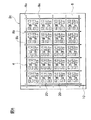
第1分割溝8aおよび8bは、図4に示すチップ状電子部品22を表面に実装した後の個別基板20を分離するための溝であり、格子状に形成される。個別基板20は、集合基板2の表面に行列状に配置され、これらの個別基板20が形成される基板領域4の周囲には、個別基板としては用いられずに廃棄処分とされるダミー領域6が形成される。
The first divided
ダミー領域6は、集合基板2の表面に電子部品を実装する際などに、良好なハンドリング特性を付与する領域などとして機能する。このダミー領域6の幅は、材料の無駄を排除する観点からは、個別基板20の縦横寸法よりも小さいことが一般的であるが、必ずしも小さくなくても良い。
The
第2分割溝10は、この実施形態では、図1において、ダミー領域6と基板領域4との境界領域に位置する一つの第1分割溝8bに連続して、その延長線上に、集合基板2の側端部まで延びるように形成してある。なお、第1分割溝8a、8bは、個別基板20を仕切り、ダミー領域6の途中までは延びているが、集合基板2の側端部までは延びないように形成してある。
In this embodiment, the
これらの第1分割溝8aおよび8bと第2分割溝10とは、図4に示すチップ状電子部品22を表面に実装する前に、集合基板2の表面に形成される。図2および図3に示すように、第1分割溝8aおよび8bの深さt1は、第2分割溝10の深さt2よりも深く形成してあり、集合基板2の厚みt0に対して、10〜90%の深さである。また、第2分割溝10の深さt2は、集合基板2の厚みt0に対して、5〜50%の深さである。
The first divided
これらの第1分割溝8aおよび8bと第2分割溝10とは、ダイヤモンド刃先、ダイヤモンド砥石、ダイヤモンドカッターなどを用いて形成される。これらの第1分割溝8aおよび8bと第2分割溝10とは、同時に形成しても良いが、別々に形成しても良い。第2分割溝10の方が浅いので、好ましくは、第2分割溝10を形成してから、第1分割溝8a,8bを形成する。これらの分割溝8a,8b,10の溝幅W0は、溝切り具に応じて決定され、ダイヤモンド刃先で形成する場合には、3〜50μm程度であれば良く、好ましくは5〜30μm、更に好ましくは10〜20μm程度、である。
The first divided
これらの第1分割溝8a,8bおよび第2分割溝10を集合基板2の表面に形成した後、基板領域4における各個別基板20の表面には、複数のチップ状電子部品22を実装する。その後に、必要に応じて、基板領域4における各個別基板20の表面を樹脂被覆し、各個別基板20の表面のチップ状電子部品22を樹脂封止する。
After the first divided
その後に、図5に示すように、第2分割溝10を含む第1分割溝8bに沿って、曲げ応力あるいは剪断応力を加えて、集合基板2を分割する。第2分割溝10は、比較的に浅いが、その溝10は、第1分割溝8bと連続していると共に、集合基板2の側端部まで延びているので、比較的に、小さな力で割ることができ、割り易い。
Thereafter, as shown in FIG. 5, the
第2分割溝10を含む第1分割溝8aに沿って集合基板2を割ると、第1分割溝8aに交差する第1分割溝8bの端部が、集合基板2の分割面30に露出することになる。そのため、その集合基板2の分割面30に露出している第1分割溝8aに沿って集合基板2を分割していくことで、次々と、個別基板20に分離していくことができる。しかも、第1分割溝8aは、比較的に深く形成してあるために、分割後の個別基板20の分割面30には、割れや欠けなどが生じにくい。したがって、本実施形態では、容易に個別基板20毎に次々と分割することができる。したがって、個別基板20の製造歩留まりも向上する。
When the
また、本実施形態に係る集合基板2では、集合基板2のダミー領域6には、比較的に浅い第2分割溝10が形成してあり、比較的に深い第1分割溝8a,8bは、ダミー領域6の途中までしか形成されていない。このため、ダミー領域6が、集合基板2全体に対して一体化される強度を付与し、集合基板2の表面に何らかの処理を行っても、第1分割溝8a,8bに沿って集合基板2が誤って分割されることはない。すなわち、本実施形態の集合基板2はハンドリング性に優れている。
第2実施形態
In the
Second embodiment
図6に示すように、本実施形態に係る集合基板2aでは、第2分割溝10を、基板領域4とダミー領域6との境界ではない中間に位置する単一の縦方向第1分割溝8bに対して直線状に連続して形成してある。
As shown in FIG. 6, in the
この実施形態の場合には、最初に分割する位置が、基板領域4とダミー領域6との境界ではない中間に位置する単一の縦方向第1分割溝8bに対して直線状の位置である以外は、前述した第1実施形態と同様であり、その説明は省略する。
第3実施形態
In the case of this embodiment, the first dividing position is a linear position with respect to a single vertical
Third embodiment
図7に示すように、本実施形態に係る集合基板2bでは、第2分割溝10を、基板領域4とダミー領域6との境界ではない中間に位置する単一の横方向第1分割溝8aに対して直線状に連続して形成してある。
As shown in FIG. 7, in the
この実施形態の場合には、最初に分割する位置が、基板領域4とダミー領域6との境界ではない中間に位置する単一の横方向第1分割溝8aに対して直線状の位置である以外は、前述した第1実施形態と同様であり、その説明は省略する。
第4実施形態
In the case of this embodiment, the position to be divided first is a linear position with respect to the single lateral first divided
Fourth embodiment
図8に示すように、本実施形態に係る集合基板2cでは、第2分割溝10を、第1分割溝8a,8bとは別に、複数の第1分割溝8aまたは8bの端部に交差するように、ダミー領域6の内部で直線状に形成してある。
As shown in FIG. 8, in the
この実施形態の場合には、最初に分割する位置が、ダミー領域6における単一の第2分割溝10に対して直線状の位置である以外は、前述した第1実施形態と同様であり、その説明は省略する。
第5実施形態
In the case of this embodiment, the first dividing position is the same as that of the first embodiment described above except that it is a linear position with respect to the single
Fifth embodiment
図9に示すように、本実施形態では、一枚の集合基板2dの表面に複数の基板領域4aが、ダミー領域6を介して配置してある。各基板領域4a毎に、複数の個別基板20aが行列状に配置してある。しかも、本実施形態では、集合基板2dにおける中央の縦方向に延びるダミー領域6と、その左側に位置する二つの基板領域4a,4aとの境界に位置する縦方向の第1分割溝8bに沿って直線状に、第2分割溝10が形成してある。その断面形状を図10に示す。
As shown in FIG. 9, in the present embodiment, a plurality of
この実施形態の場合には、最初に分割する位置が、図9および図10に示す第2分割溝10の直線状位置である以外は、前述した第1実施形態と同様であり、その説明は省略する。
In the case of this embodiment, the first dividing position is the same as that of the first embodiment described above except that it is the linear position of the
なお、本発明は、上述した実施形態に限定されるものではなく、本発明の範囲内で種々に改変することができる。 The present invention is not limited to the above-described embodiment, and can be variously modified within the scope of the present invention.
たとえば、上述した実施形態では、一つの集合基板に対して第2分割溝10を一直線状に形成したが、本発明では、2つ以上の直線状に第2分割溝10を形成しても良い。たとえば図1において、ダミー領域6と基板領域4との2〜4の境界領域に位置する第1分割溝8a、8bに連続して、それぞれ2〜4の直線状に第2分割溝10を形成しても良い。
For example, in the above-described embodiment, the second divided
また、上述した実施形態では、第1分割溝および第2分割溝を全て直線状に形成したが、本発明では、必要に応じて、一部または全部において曲線や折れ線形状を含んでも良い。 In the embodiment described above, the first divided grooves and the second divided grooves are all formed in a straight line shape. However, in the present invention, a part or the whole may include a curved line or a polygonal line shape as necessary.
さらに、本発明は、LTCC基板(低温同時焼成セラミック基板)などのガラスセラミック基板に限定されず、その他のセラミック基板、樹脂基板、複合積層基板などにも適用することができる。 Furthermore, the present invention is not limited to a glass ceramic substrate such as an LTCC substrate (low temperature co-fired ceramic substrate), but can be applied to other ceramic substrates, resin substrates, composite laminated substrates, and the like.
2,2a〜2d… 集合基板
4,4a… 基板領域
6… ダミー領域
8a,8b… 第1分割溝
10… 第2分割溝
20,20a… 個別基板
22… チップ状電子部品
30… 分割面
2, 2a to 2d ...
Claims (11)
前記基板領域では、前記個別基板を仕切り、前記ダミー領域の途中まで延びており、前記集合基板の側端部までは延びていない第1深さの複数の第1分割溝が行列状に形成してあり、
前記ダミー領域には、前記集合基板の側端部まで延びるように、前記第1深さよりも浅い第2深さの第2分割溝が少なくとも一つ形成してあることを特徴とする集合基板。 A collective substrate in which a substrate region that becomes a plurality of individual substrates after division and a dummy region that is discarded instead of an individual substrate is formed,
In the substrate region, the individual substrates are partitioned and extend to the middle of the dummy region, and a plurality of first division grooves having a first depth that does not extend to the side edges of the collective substrate are formed in a matrix. And
The aggregate substrate, wherein at least one second division groove having a second depth shallower than the first depth is formed in the dummy region so as to extend to a side end portion of the aggregate substrate.
前記個別基板毎に仕切り、前記ダミー領域の途中まで延びており、前記集合基板の側端部までは延びていない第1深さの複数の第1分割溝を、焼成後の前記集合基板に行列状に形成する工程と、
前記ダミー領域に、前記集合基板の側端部まで延びるように、前記第1深さよりも浅い第2深さの第2分割溝を少なくとも一つ形成する工程と、
前記第2分割溝に沿って、前記集合基板を割った後に、前記第1分割溝に沿って前記集合基板を割り、前記個別基板毎に分割する工程と、を有する個別基板の製造方法。 Firing a collective substrate having a substrate region that becomes a plurality of individual substrates after the division and a dummy region that is discarded instead of being an individual substrate;
A plurality of first division grooves having a first depth that are partitioned for each individual substrate and extend to the middle of the dummy region and do not extend to the side edge of the collective substrate are arranged in a matrix on the fired collective substrate. Forming into a shape,
Forming at least one second division groove having a second depth shallower than the first depth so as to extend to a side edge of the collective substrate in the dummy region;
Dividing the aggregate substrate along the second divided groove, then dividing the aggregate substrate along the first divided groove, and dividing the divided substrate into individual substrates.
Priority Applications (1)
| Application Number | Priority Date | Filing Date | Title |
|---|---|---|---|
| JP2006077512A JP2007258264A (en) | 2006-03-20 | 2006-03-20 | Assembled substrate, and manufacturing method of individual substrate |
Applications Claiming Priority (1)
| Application Number | Priority Date | Filing Date | Title |
|---|---|---|---|
| JP2006077512A JP2007258264A (en) | 2006-03-20 | 2006-03-20 | Assembled substrate, and manufacturing method of individual substrate |
Publications (1)
| Publication Number | Publication Date |
|---|---|
| JP2007258264A true JP2007258264A (en) | 2007-10-04 |
Family
ID=38632226
Family Applications (1)
| Application Number | Title | Priority Date | Filing Date |
|---|---|---|---|
| JP2006077512A Pending JP2007258264A (en) | 2006-03-20 | 2006-03-20 | Assembled substrate, and manufacturing method of individual substrate |
Country Status (1)
| Country | Link |
|---|---|
| JP (1) | JP2007258264A (en) |
Cited By (3)
| Publication number | Priority date | Publication date | Assignee | Title |
|---|---|---|---|---|
| JP2010027665A (en) * | 2008-07-15 | 2010-02-04 | Alps Electric Co Ltd | Method of manufacturing ceramic multilayered wiring board, and ceramic multilayered wiring board |
| US8024857B2 (en) | 2008-11-07 | 2011-09-27 | Hynix Semiconductor Inc. | Substrate for semiconductor package having a reinforcing member that prevents distortions and method for fabricating the same |
| CN110770184A (en) * | 2017-06-15 | 2020-02-07 | 康宁股份有限公司 | Article capable of being divided individually |
-
2006
- 2006-03-20 JP JP2006077512A patent/JP2007258264A/en active Pending
Cited By (4)
| Publication number | Priority date | Publication date | Assignee | Title |
|---|---|---|---|---|
| JP2010027665A (en) * | 2008-07-15 | 2010-02-04 | Alps Electric Co Ltd | Method of manufacturing ceramic multilayered wiring board, and ceramic multilayered wiring board |
| US8024857B2 (en) | 2008-11-07 | 2011-09-27 | Hynix Semiconductor Inc. | Substrate for semiconductor package having a reinforcing member that prevents distortions and method for fabricating the same |
| CN110770184A (en) * | 2017-06-15 | 2020-02-07 | 康宁股份有限公司 | Article capable of being divided individually |
| CN110770184B (en) * | 2017-06-15 | 2023-03-28 | 康宁股份有限公司 | Individually dividable article |
Similar Documents
| Publication | Publication Date | Title |
|---|---|---|
| US8105453B2 (en) | Method for producing multilayer ceramic substrate | |
| US7833370B2 (en) | Method for manufacturing a ceramic multi-layered substrate | |
| JPWO2002043455A1 (en) | Manufacturing method of ceramic multilayer substrate and unfired composite laminate | |
| JP2003246680A (en) | Method of manufacturing multilayered ceramic substrate | |
| JP2007258264A (en) | Assembled substrate, and manufacturing method of individual substrate | |
| JP4190555B2 (en) | Multi-piece wiring board and manufacturing method thereof | |
| JP2006278761A (en) | Manufacturing method of green substrate, breaking method of ceramic substrate, and manufacturing method of chip electric component | |
| JP2008028065A (en) | Method for manufacturing ceramic substrate | |
| JPH09260844A (en) | Ceramic multilayered board manufacturing method | |
| JP2007165540A (en) | Method for manufacturing multilayer ceramic substrate, and the multilayer ceramic aggregate substrate | |
| JP4317856B2 (en) | Manufacturing method of individual substrates | |
| JP4110536B2 (en) | Multilayer ceramic aggregate substrate and method for producing multilayer ceramic aggregate substrate | |
| JP4888564B2 (en) | Manufacturing method of ceramic multilayer substrate with cavity | |
| JP2006173368A (en) | Ceramic substrate | |
| JP4550243B2 (en) | Manufacturing method of glass ceramic substrate | |
| JP4645962B2 (en) | Multilayer ceramic substrate | |
| JP5517840B2 (en) | Method for producing green sheet laminate and method for producing insulating substrate | |
| JP2011018783A (en) | Method of manufacturing multilayer ceramic substrate | |
| JP4610185B2 (en) | Wiring board and manufacturing method thereof | |
| JP4132026B2 (en) | Large ceramic substrate | |
| JP2006278760A (en) | Method and apparatus for manufacturing glass ceramic aggregate substrate | |
| JP3909182B2 (en) | Manufacturing method of glass ceramic substrate | |
| JP2004296721A (en) | Large board for obtaining a plurality of wiring boards | |
| JP2009087965A (en) | Multilayer wiring board | |
| JP2002160978A (en) | Method for manufacturing glass ceramic substrate |
Legal Events
| Date | Code | Title | Description |
|---|---|---|---|
| A977 | Report on retrieval |
Effective date: 20080325 Free format text: JAPANESE INTERMEDIATE CODE: A971007 |
|
| A131 | Notification of reasons for refusal |
Effective date: 20080415 Free format text: JAPANESE INTERMEDIATE CODE: A131 |
|
| A521 | Written amendment |
Effective date: 20080611 Free format text: JAPANESE INTERMEDIATE CODE: A523 |
|
| A02 | Decision of refusal |
Effective date: 20080715 Free format text: JAPANESE INTERMEDIATE CODE: A02 |