JP2007201314A - Semiconductor device - Google Patents
Semiconductor device Download PDFInfo
- Publication number
- JP2007201314A JP2007201314A JP2006020221A JP2006020221A JP2007201314A JP 2007201314 A JP2007201314 A JP 2007201314A JP 2006020221 A JP2006020221 A JP 2006020221A JP 2006020221 A JP2006020221 A JP 2006020221A JP 2007201314 A JP2007201314 A JP 2007201314A
- Authority
- JP
- Japan
- Prior art keywords
- semiconductor element
- mounting substrate
- bonded
- semiconductor device
- region
- Prior art date
- Legal status (The legal status is an assumption and is not a legal conclusion. Google has not performed a legal analysis and makes no representation as to the accuracy of the status listed.)
- Pending
Links
Images


Classifications
-
- H—ELECTRICITY
- H01—ELECTRIC ELEMENTS
- H01L—SEMICONDUCTOR DEVICES NOT COVERED BY CLASS H10
- H01L24/00—Arrangements for connecting or disconnecting semiconductor or solid-state bodies; Methods or apparatus related thereto
- H01L24/01—Means for bonding being attached to, or being formed on, the surface to be connected, e.g. chip-to-package, die-attach, "first-level" interconnects; Manufacturing methods related thereto
- H01L24/26—Layer connectors, e.g. plate connectors, solder or adhesive layers; Manufacturing methods related thereto
- H01L24/28—Structure, shape, material or disposition of the layer connectors prior to the connecting process
- H01L24/29—Structure, shape, material or disposition of the layer connectors prior to the connecting process of an individual layer connector
-
- H—ELECTRICITY
- H01—ELECTRIC ELEMENTS
- H01L—SEMICONDUCTOR DEVICES NOT COVERED BY CLASS H10
- H01L24/00—Arrangements for connecting or disconnecting semiconductor or solid-state bodies; Methods or apparatus related thereto
- H01L24/01—Means for bonding being attached to, or being formed on, the surface to be connected, e.g. chip-to-package, die-attach, "first-level" interconnects; Manufacturing methods related thereto
- H01L24/26—Layer connectors, e.g. plate connectors, solder or adhesive layers; Manufacturing methods related thereto
- H01L24/28—Structure, shape, material or disposition of the layer connectors prior to the connecting process
- H01L24/30—Structure, shape, material or disposition of the layer connectors prior to the connecting process of a plurality of layer connectors
-
- H—ELECTRICITY
- H01—ELECTRIC ELEMENTS
- H01L—SEMICONDUCTOR DEVICES NOT COVERED BY CLASS H10
- H01L24/00—Arrangements for connecting or disconnecting semiconductor or solid-state bodies; Methods or apparatus related thereto
- H01L24/01—Means for bonding being attached to, or being formed on, the surface to be connected, e.g. chip-to-package, die-attach, "first-level" interconnects; Manufacturing methods related thereto
- H01L24/26—Layer connectors, e.g. plate connectors, solder or adhesive layers; Manufacturing methods related thereto
- H01L24/31—Structure, shape, material or disposition of the layer connectors after the connecting process
- H01L24/32—Structure, shape, material or disposition of the layer connectors after the connecting process of an individual layer connector
-
- H—ELECTRICITY
- H01—ELECTRIC ELEMENTS
- H01L—SEMICONDUCTOR DEVICES NOT COVERED BY CLASS H10
- H01L24/00—Arrangements for connecting or disconnecting semiconductor or solid-state bodies; Methods or apparatus related thereto
- H01L24/01—Means for bonding being attached to, or being formed on, the surface to be connected, e.g. chip-to-package, die-attach, "first-level" interconnects; Manufacturing methods related thereto
- H01L24/26—Layer connectors, e.g. plate connectors, solder or adhesive layers; Manufacturing methods related thereto
- H01L24/31—Structure, shape, material or disposition of the layer connectors after the connecting process
- H01L24/33—Structure, shape, material or disposition of the layer connectors after the connecting process of a plurality of layer connectors
-
- H—ELECTRICITY
- H01—ELECTRIC ELEMENTS
- H01L—SEMICONDUCTOR DEVICES NOT COVERED BY CLASS H10
- H01L2224/00—Indexing scheme for arrangements for connecting or disconnecting semiconductor or solid-state bodies and methods related thereto as covered by H01L24/00
- H01L2224/01—Means for bonding being attached to, or being formed on, the surface to be connected, e.g. chip-to-package, die-attach, "first-level" interconnects; Manufacturing methods related thereto
- H01L2224/26—Layer connectors, e.g. plate connectors, solder or adhesive layers; Manufacturing methods related thereto
- H01L2224/2612—Auxiliary members for layer connectors, e.g. spacers
- H01L2224/26152—Auxiliary members for layer connectors, e.g. spacers being formed on an item to be connected not being a semiconductor or solid-state body
- H01L2224/26175—Flow barriers
-
- H—ELECTRICITY
- H01—ELECTRIC ELEMENTS
- H01L—SEMICONDUCTOR DEVICES NOT COVERED BY CLASS H10
- H01L2224/00—Indexing scheme for arrangements for connecting or disconnecting semiconductor or solid-state bodies and methods related thereto as covered by H01L24/00
- H01L2224/01—Means for bonding being attached to, or being formed on, the surface to be connected, e.g. chip-to-package, die-attach, "first-level" interconnects; Manufacturing methods related thereto
- H01L2224/26—Layer connectors, e.g. plate connectors, solder or adhesive layers; Manufacturing methods related thereto
- H01L2224/28—Structure, shape, material or disposition of the layer connectors prior to the connecting process
- H01L2224/29—Structure, shape, material or disposition of the layer connectors prior to the connecting process of an individual layer connector
- H01L2224/29001—Core members of the layer connector
- H01L2224/29005—Structure
- H01L2224/29006—Layer connector larger than the underlying bonding area
-
- H—ELECTRICITY
- H01—ELECTRIC ELEMENTS
- H01L—SEMICONDUCTOR DEVICES NOT COVERED BY CLASS H10
- H01L2224/00—Indexing scheme for arrangements for connecting or disconnecting semiconductor or solid-state bodies and methods related thereto as covered by H01L24/00
- H01L2224/01—Means for bonding being attached to, or being formed on, the surface to be connected, e.g. chip-to-package, die-attach, "first-level" interconnects; Manufacturing methods related thereto
- H01L2224/26—Layer connectors, e.g. plate connectors, solder or adhesive layers; Manufacturing methods related thereto
- H01L2224/28—Structure, shape, material or disposition of the layer connectors prior to the connecting process
- H01L2224/29—Structure, shape, material or disposition of the layer connectors prior to the connecting process of an individual layer connector
- H01L2224/29001—Core members of the layer connector
- H01L2224/2901—Shape
- H01L2224/29011—Shape comprising apertures or cavities
-
- H—ELECTRICITY
- H01—ELECTRIC ELEMENTS
- H01L—SEMICONDUCTOR DEVICES NOT COVERED BY CLASS H10
- H01L2224/00—Indexing scheme for arrangements for connecting or disconnecting semiconductor or solid-state bodies and methods related thereto as covered by H01L24/00
- H01L2224/01—Means for bonding being attached to, or being formed on, the surface to be connected, e.g. chip-to-package, die-attach, "first-level" interconnects; Manufacturing methods related thereto
- H01L2224/26—Layer connectors, e.g. plate connectors, solder or adhesive layers; Manufacturing methods related thereto
- H01L2224/28—Structure, shape, material or disposition of the layer connectors prior to the connecting process
- H01L2224/29—Structure, shape, material or disposition of the layer connectors prior to the connecting process of an individual layer connector
- H01L2224/29001—Core members of the layer connector
- H01L2224/2902—Disposition
- H01L2224/29034—Disposition the layer connector covering only portions of the surface to be connected
- H01L2224/29035—Disposition the layer connector covering only portions of the surface to be connected covering only the peripheral area of the surface to be connected
-
- H—ELECTRICITY
- H01—ELECTRIC ELEMENTS
- H01L—SEMICONDUCTOR DEVICES NOT COVERED BY CLASS H10
- H01L2224/00—Indexing scheme for arrangements for connecting or disconnecting semiconductor or solid-state bodies and methods related thereto as covered by H01L24/00
- H01L2224/01—Means for bonding being attached to, or being formed on, the surface to be connected, e.g. chip-to-package, die-attach, "first-level" interconnects; Manufacturing methods related thereto
- H01L2224/26—Layer connectors, e.g. plate connectors, solder or adhesive layers; Manufacturing methods related thereto
- H01L2224/28—Structure, shape, material or disposition of the layer connectors prior to the connecting process
- H01L2224/29—Structure, shape, material or disposition of the layer connectors prior to the connecting process of an individual layer connector
- H01L2224/29001—Core members of the layer connector
- H01L2224/2902—Disposition
- H01L2224/29034—Disposition the layer connector covering only portions of the surface to be connected
- H01L2224/29036—Disposition the layer connector covering only portions of the surface to be connected covering only the central area of the surface to be connected
-
- H—ELECTRICITY
- H01—ELECTRIC ELEMENTS
- H01L—SEMICONDUCTOR DEVICES NOT COVERED BY CLASS H10
- H01L2224/00—Indexing scheme for arrangements for connecting or disconnecting semiconductor or solid-state bodies and methods related thereto as covered by H01L24/00
- H01L2224/01—Means for bonding being attached to, or being formed on, the surface to be connected, e.g. chip-to-package, die-attach, "first-level" interconnects; Manufacturing methods related thereto
- H01L2224/26—Layer connectors, e.g. plate connectors, solder or adhesive layers; Manufacturing methods related thereto
- H01L2224/28—Structure, shape, material or disposition of the layer connectors prior to the connecting process
- H01L2224/29—Structure, shape, material or disposition of the layer connectors prior to the connecting process of an individual layer connector
- H01L2224/29001—Core members of the layer connector
- H01L2224/29075—Plural core members
- H01L2224/29076—Plural core members being mutually engaged together, e.g. through inserts
-
- H—ELECTRICITY
- H01—ELECTRIC ELEMENTS
- H01L—SEMICONDUCTOR DEVICES NOT COVERED BY CLASS H10
- H01L2224/00—Indexing scheme for arrangements for connecting or disconnecting semiconductor or solid-state bodies and methods related thereto as covered by H01L24/00
- H01L2224/01—Means for bonding being attached to, or being formed on, the surface to be connected, e.g. chip-to-package, die-attach, "first-level" interconnects; Manufacturing methods related thereto
- H01L2224/26—Layer connectors, e.g. plate connectors, solder or adhesive layers; Manufacturing methods related thereto
- H01L2224/28—Structure, shape, material or disposition of the layer connectors prior to the connecting process
- H01L2224/29—Structure, shape, material or disposition of the layer connectors prior to the connecting process of an individual layer connector
- H01L2224/29001—Core members of the layer connector
- H01L2224/29075—Plural core members
- H01L2224/29078—Plural core members being disposed next to each other, e.g. side-to-side arrangements
-
- H—ELECTRICITY
- H01—ELECTRIC ELEMENTS
- H01L—SEMICONDUCTOR DEVICES NOT COVERED BY CLASS H10
- H01L2224/00—Indexing scheme for arrangements for connecting or disconnecting semiconductor or solid-state bodies and methods related thereto as covered by H01L24/00
- H01L2224/01—Means for bonding being attached to, or being formed on, the surface to be connected, e.g. chip-to-package, die-attach, "first-level" interconnects; Manufacturing methods related thereto
- H01L2224/26—Layer connectors, e.g. plate connectors, solder or adhesive layers; Manufacturing methods related thereto
- H01L2224/28—Structure, shape, material or disposition of the layer connectors prior to the connecting process
- H01L2224/30—Structure, shape, material or disposition of the layer connectors prior to the connecting process of a plurality of layer connectors
- H01L2224/3005—Shape
- H01L2224/30051—Layer connectors having different shapes
-
- H—ELECTRICITY
- H01—ELECTRIC ELEMENTS
- H01L—SEMICONDUCTOR DEVICES NOT COVERED BY CLASS H10
- H01L2224/00—Indexing scheme for arrangements for connecting or disconnecting semiconductor or solid-state bodies and methods related thereto as covered by H01L24/00
- H01L2224/01—Means for bonding being attached to, or being formed on, the surface to be connected, e.g. chip-to-package, die-attach, "first-level" interconnects; Manufacturing methods related thereto
- H01L2224/26—Layer connectors, e.g. plate connectors, solder or adhesive layers; Manufacturing methods related thereto
- H01L2224/31—Structure, shape, material or disposition of the layer connectors after the connecting process
- H01L2224/32—Structure, shape, material or disposition of the layer connectors after the connecting process of an individual layer connector
- H01L2224/3201—Structure
- H01L2224/32012—Structure relative to the bonding area, e.g. bond pad
- H01L2224/32013—Structure relative to the bonding area, e.g. bond pad the layer connector being larger than the bonding area, e.g. bond pad
-
- H—ELECTRICITY
- H01—ELECTRIC ELEMENTS
- H01L—SEMICONDUCTOR DEVICES NOT COVERED BY CLASS H10
- H01L2224/00—Indexing scheme for arrangements for connecting or disconnecting semiconductor or solid-state bodies and methods related thereto as covered by H01L24/00
- H01L2224/01—Means for bonding being attached to, or being formed on, the surface to be connected, e.g. chip-to-package, die-attach, "first-level" interconnects; Manufacturing methods related thereto
- H01L2224/26—Layer connectors, e.g. plate connectors, solder or adhesive layers; Manufacturing methods related thereto
- H01L2224/31—Structure, shape, material or disposition of the layer connectors after the connecting process
- H01L2224/32—Structure, shape, material or disposition of the layer connectors after the connecting process of an individual layer connector
- H01L2224/3201—Structure
- H01L2224/32012—Structure relative to the bonding area, e.g. bond pad
- H01L2224/32014—Structure relative to the bonding area, e.g. bond pad the layer connector being smaller than the bonding area, e.g. bond pad
-
- H—ELECTRICITY
- H01—ELECTRIC ELEMENTS
- H01L—SEMICONDUCTOR DEVICES NOT COVERED BY CLASS H10
- H01L2224/00—Indexing scheme for arrangements for connecting or disconnecting semiconductor or solid-state bodies and methods related thereto as covered by H01L24/00
- H01L2224/01—Means for bonding being attached to, or being formed on, the surface to be connected, e.g. chip-to-package, die-attach, "first-level" interconnects; Manufacturing methods related thereto
- H01L2224/26—Layer connectors, e.g. plate connectors, solder or adhesive layers; Manufacturing methods related thereto
- H01L2224/31—Structure, shape, material or disposition of the layer connectors after the connecting process
- H01L2224/33—Structure, shape, material or disposition of the layer connectors after the connecting process of a plurality of layer connectors
- H01L2224/3301—Structure
-
- H—ELECTRICITY
- H01—ELECTRIC ELEMENTS
- H01L—SEMICONDUCTOR DEVICES NOT COVERED BY CLASS H10
- H01L2924/00—Indexing scheme for arrangements or methods for connecting or disconnecting semiconductor or solid-state bodies as covered by H01L24/00
- H01L2924/15—Details of package parts other than the semiconductor or other solid state devices to be connected
- H01L2924/151—Die mounting substrate
- H01L2924/1515—Shape
- H01L2924/15151—Shape the die mounting substrate comprising an aperture, e.g. for underfilling, outgassing, window type wire connections
-
- H—ELECTRICITY
- H01—ELECTRIC ELEMENTS
- H01L—SEMICONDUCTOR DEVICES NOT COVERED BY CLASS H10
- H01L2924/00—Indexing scheme for arrangements or methods for connecting or disconnecting semiconductor or solid-state bodies as covered by H01L24/00
- H01L2924/30—Technical effects
- H01L2924/35—Mechanical effects
- H01L2924/351—Thermal stress
Landscapes
- Engineering & Computer Science (AREA)
- Computer Hardware Design (AREA)
- Microelectronics & Electronic Packaging (AREA)
- Power Engineering (AREA)
- Wire Bonding (AREA)
Abstract
Description
本発明は、半導体素子が接合層によって実装基板に接合されている半導体装置に関し、特に、半導体素子内の位置による電気抵抗率のばらつきが小さい半導体装置に関する。 The present invention relates to a semiconductor device in which a semiconductor element is bonded to a mounting substrate by a bonding layer, and more particularly to a semiconductor device in which variation in electrical resistivity due to a position in the semiconductor element is small.
半導体装置は、一般的に、スイッチング素子等を構成する半導体素子が接合層によって実装基板に接合されている。
例えば、図22に示すように、特許文献1の半導体装置100では、半導体素子110が接合層130によって実装基板120に接合されている。実装基板120には、半導体素子110の冷却を促進するために、熱伝導率の高いCu又はAl等の金属基板が用いられ、接合層130には、はんだが用いられる。なお、接合層130に、はんだ以外の金属や接着剤等が用いられる場合もある。
For example, as shown in FIG. 22, in the
半導体素子110を接合層130によって実装基板120に接合する際には、加熱接合することが多い。また、実装基板120の主材料(Cu,Al等)の線膨張係数は、半導体素子110の主材料(Si,GaN等)の線膨張係数よりも大きい場合が多い。接合層130の厚みは、半導体素子110や実装基板120の厚みと比較して薄いので、実装基板120と半導体素子110の線膨張係数の差が、実装基板120と半導体素子110の接合状態に影響を及ぼす。半導体素子110を実装基板120に加熱接合した後に、動作温度(例えば、20〜30℃)にまで温度を下げると、半導体素子110よりも実装基板120の線膨張係数が大きいため、半導体素子110に半導体素子110を中央部に向けて圧縮する熱応力が発生する。
この場合、半導体素子110に発生する熱応力は、半導体素子110の周辺部において相対的に小さく、中央部において相対的に大きくなりやすい。半導体素子110内の位置によって熱応力の値がばらつくと、ピエゾ抵抗効果によって半導体素子110を構成する材料の電気抵抗率が変化することから、半導体素子110内の位置によって電気抵抗率がばらついてしまう。すると、半導体素子がオンした際に、電気抵抗率が低い部分に電流が集中し、この部分が局所的に発熱し易い。
本発明は、上記の問題点を解決するために創案された。本発明では、実装基板に接合されている半導体素子の電気抵抗率が半導体素子内の位置によってばらつく度合いが小さい半導体装置を提供する。
When the
In this case, the thermal stress generated in the
The present invention has been devised to solve the above problems. The present invention provides a semiconductor device in which the electrical resistivity of a semiconductor element bonded to a mounting substrate has a small degree of variation depending on the position in the semiconductor element.
(請求項1に記載の発明)
本発明の半導体装置では、半導体素子が接合層によって実装基板に接合されている。本発明の半導体装置では、接合層と実装基板の少なくとも一方が、半導体素子の周辺部に接合している領域と半導体素子の中央部に接合している領域とで、材料組成が異なっていることを特徴とする。
ここでいう「半導体素子の周辺部」は、半導体素子の周囲の全範囲を意味する場合もあれば、半導体素子の周囲の一部の範囲を意味する場合もある。たとえば、半導体素子の平面形状が略四角形に形成されている場合には、四辺に隣接する範囲であることもあれば、対向する二辺に隣接する範囲のみであることもある。「半導体素子の中央部」は、半導体素子の周辺部に囲まれている範囲を意味する場合もあれば、中心を含む範囲であって上記した「周辺部」以外の全ての範囲を意味する場合もあれば、「周辺部」以外の一部の範囲を意味する場合もある。典型的には、「中央部」には、半導体素子の主動作領域が配設されており、「周辺部」には、主動作領域が配設されていない。「周辺部」には、例えば周辺耐圧領域やワイヤ等とのボンディング領域が形成されている。
(Invention of Claim 1)
In the semiconductor device of the present invention, the semiconductor element is bonded to the mounting substrate by the bonding layer. In the semiconductor device of the present invention, the material composition of at least one of the bonding layer and the mounting substrate is different between the region bonded to the peripheral portion of the semiconductor element and the region bonded to the central portion of the semiconductor element. It is characterized by.
The “peripheral portion of the semiconductor element” as used herein may mean the entire range around the semiconductor element, or it may mean a partial range around the semiconductor element. For example, when the planar shape of the semiconductor element is formed in a substantially square shape, it may be a range adjacent to four sides or only a range adjacent to two opposite sides. “Central part of the semiconductor element” may mean a range surrounded by the peripheral part of the semiconductor element, or may mean a range including the center and other than the above “peripheral part” In other cases, it may mean a part of the range other than the “peripheral portion”. Typically, the main operation region of the semiconductor element is disposed in the “central portion”, and the main operation region is not disposed in the “peripheral portion”. In the “peripheral portion”, for example, a peripheral pressure-resistant region or a bonding region with a wire or the like is formed.
従来の技術の欄で記載したように、一般的に、半導体素子を接合層によって実装基板に加熱接合した後に温度を下げると、半導体素子に熱応力が発生する。実装基板の材料組成が一様であり、接合層の材料組成が一様であると、半導体素子の中心に近いほど半導体素子に発生する熱応力が大きくなる。
本発明の半導体装置の場合、接合層と実装基板の少なくとも一方では、半導体素子の周辺部に接合している領域と半導体素子の中央部に接合している領域とで、材料組成が変えてある。材料組成を変えることによって、熱応力が集中しやすい半導体装置の中央部では実装基板による機械的拘束力を弱め、熱応力が集中しづらい半導体装置の周辺部では実装基板による機械的拘束力を強めることができる。これにより、半導体素子は周辺部において相対的に強固に実装基板に固定され、中央部では相対的にフリーな状態におかれる。これによって、半導体素子を実装基板に確実に接合するとともに、中心に近い程大きくなっていた熱応力の分布を一様化することができる。したがって、ピエゾ抵抗効果によって、電気抵抗率が半導体素子内の位置によってばらついてしまう現象の発生を抑制することができる。半導体素子がオン状態の際に、応力集中とピエゾ抵抗効果によって、電気抵抗率が低くなった部分に電流が集中し、この部分が局所的に発熱するのを防止することができる。
As described in the section of the prior art, generally, when the temperature is lowered after the semiconductor element is heated and bonded to the mounting substrate with the bonding layer, thermal stress is generated in the semiconductor element. If the material composition of the mounting substrate is uniform and the material composition of the bonding layer is uniform, the closer to the center of the semiconductor element, the greater the thermal stress generated in the semiconductor element.
In the case of the semiconductor device of the present invention, at least one of the bonding layer and the mounting substrate has a different material composition between the region bonded to the peripheral portion of the semiconductor element and the region bonded to the central portion of the semiconductor element. . By changing the material composition, the mechanical restraint force due to the mounting substrate is weakened at the center of the semiconductor device where thermal stress is likely to concentrate, and the mechanical restraint force due to the mounting substrate is strengthened at the periphery of the semiconductor device where thermal stress is difficult to concentrate. be able to. Thereby, the semiconductor element is relatively firmly fixed to the mounting substrate in the peripheral portion, and is relatively free in the central portion. As a result, the semiconductor element can be reliably bonded to the mounting substrate, and the distribution of thermal stress that has become larger as it is closer to the center can be made uniform. Therefore, it is possible to suppress the occurrence of the phenomenon that the electric resistivity varies depending on the position in the semiconductor element due to the piezoresistance effect. When the semiconductor element is in the ON state, current can be prevented from being concentrated in a portion where the electrical resistivity is low due to stress concentration and the piezoresistive effect, and this portion can be prevented from generating heat locally.
(請求項2に記載の発明)
半導体素子と実装基板を接合する接合層が、半導体素子の周辺部を実装基板に接合している領域では引っ張り強度が高い材料組成を有し、半導体素子の中央部を実装基板に接合している領域では引っ張り強度が低い材料組成を有していてもよい。
この場合、半導体素子は、周辺部において強く拘束され、中央部では弱く拘束される。従って、半導体素子は、周辺部において強く拘束された状態で実装基板に接合される。この場合、半導体素子の中心に近づくほど熱応力が発達する現象が抑制される。半導体素子内の位置によって熱応力が大きく分布する現象を抑制することができる。
(Invention of Claim 2)
The bonding layer for bonding the semiconductor element and the mounting substrate has a material composition having high tensile strength in the region where the peripheral portion of the semiconductor element is bonded to the mounting substrate, and the central portion of the semiconductor element is bonded to the mounting substrate. The region may have a material composition with low tensile strength.
In this case, the semiconductor element is strongly restrained at the peripheral portion and weakly restrained at the central portion. Therefore, the semiconductor element is bonded to the mounting substrate in a state of being strongly restrained at the peripheral portion. In this case, a phenomenon in which thermal stress develops as the position approaches the center of the semiconductor element is suppressed. A phenomenon in which thermal stress is largely distributed depending on the position in the semiconductor element can be suppressed.
(請求項3に記載の発明)
半導体素子と実装基板を接合する接合層が、半導体素子の周辺部を実装基板に接合している領域では融点が高い材料組成を有し、半導体素子の中央部を実装基板に接合している領域では融点が低い材料組成を有していてもよい。
この場合、半導体素子の周辺部は高い温度状態で実装基板に拘束され、中央部は低い温度状態で実装基板に拘束される。すなわち、半導体素子の周辺部が実装基板に拘束される時の温度と半導体素子の動作温度の差に比して、半導体素子の中央部が実装基板に拘束される時の温度と半導体素子の動作温度の差は小さい。半導体素子に加わる熱応力は、前記の温度差が小さいほど小さい。従って、半導体素子の中央部において、大きな熱応力が発達することを防止できる。半導体素子内の位置によって熱応力が大きく分布する現象を抑制することができる。
(Invention of Claim 3)
A region in which the bonding layer for bonding the semiconductor element and the mounting substrate has a material composition with a high melting point in the region where the peripheral portion of the semiconductor element is bonded to the mounting substrate, and the central portion of the semiconductor element is bonded to the mounting substrate Then, you may have a material composition with low melting | fusing point.
In this case, the peripheral portion of the semiconductor element is restrained by the mounting substrate at a high temperature state, and the central portion is restrained by the mounting substrate at a low temperature state. That is, the temperature when the central part of the semiconductor element is restrained by the mounting substrate and the operation of the semiconductor element, compared to the difference between the temperature when the peripheral part of the semiconductor element is restrained by the mounting substrate and the operating temperature of the semiconductor element. The difference in temperature is small. The thermal stress applied to the semiconductor element is smaller as the temperature difference is smaller. Therefore, it is possible to prevent a large thermal stress from developing in the central portion of the semiconductor element. A phenomenon in which thermal stress is largely distributed depending on the position in the semiconductor element can be suppressed.
(請求項4に記載の発明)
実装基板が、接合層によって半導体素子の周辺部に接合している領域では線膨張係数が大きい材料組成を有し、接合層によって半導体素子の中央部を接合している領域では線膨張係数が小さい材料組成を有していてもよい。
この場合、半導体素子を実装基板に加熱接合してから半導体素子の動作温度にまで温度を下げた場合に、半導体素子の中央部が接合される実装基板では収縮率が小さいに対し、半導体素子の周辺部が接合される実装基板では収縮率が大きい。従って、半導体素子の中央部において熱応力が発達する程度が低減される。半導体素子内の位置によって熱応力が大きく分布する現象を抑制することができる。
(Invention of Claim 4)
The region where the mounting substrate is bonded to the peripheral portion of the semiconductor element by the bonding layer has a material composition having a large linear expansion coefficient, and the region where the central portion of the semiconductor element is bonded by the bonding layer is small. It may have a material composition.
In this case, when the temperature is lowered to the operating temperature of the semiconductor element after the semiconductor element is heated and bonded to the mounting substrate, the shrinkage rate is small in the mounting substrate to which the central portion of the semiconductor element is bonded, whereas The shrinkage rate is large in the mounting substrate to which the peripheral part is bonded. Therefore, the degree to which the thermal stress develops in the central portion of the semiconductor element is reduced. A phenomenon in which thermal stress is largely distributed depending on the position in the semiconductor element can be suppressed.
(請求項5に記載の発明)
実装基板を多孔質の母材で構成することができ、多孔質の母材の孔に母材とは相違する線膨張係数を有する部材を配設することができる。この場合、接合層によって半導体素子の周辺部に接合されている領域と、接合層によって半導体素子の中央部に接合されている領域とで、前記孔に配設されている部材の量を相違させることによって、半導体素子の周辺部に接合されている実装基板の線膨張係数の方が、半導体素子の中央部に接合されている実装基板の線膨張係数よりも大きくすることができる。
本発明の半導体装置によれば、半導体素子の周辺部に接合されている実装基板の線膨張係数と中央部に接合されている実装基板の線膨張係数の関係を簡単に調節することができる。
(Invention of Claim 5)
The mounting substrate can be formed of a porous base material, and a member having a linear expansion coefficient different from that of the base material can be disposed in the hole of the porous base material. In this case, the amount of the member disposed in the hole is different between the region bonded to the peripheral portion of the semiconductor element by the bonding layer and the region bonded to the central portion of the semiconductor element by the bonding layer. Accordingly, the linear expansion coefficient of the mounting substrate bonded to the peripheral portion of the semiconductor element can be made larger than the linear expansion coefficient of the mounting substrate bonded to the central portion of the semiconductor element.
According to the semiconductor device of the present invention, the relationship between the linear expansion coefficient of the mounting substrate bonded to the peripheral portion of the semiconductor element and the linear expansion coefficient of the mounting substrate bonded to the central portion can be easily adjusted.
多孔質の母材の孔に、母材よりも大きな線膨張係数を有する部材を配設してもよいし、小さな線膨張係数を有する部材を配設してもよい。小さな線膨張係数を有する部材を配設する場合には、例えば以下の構成を採用することができる。
典型的には、母材の孔は基本的に同じサイズとし、半導体素子の周辺部に対応する領域では孔の密度を低くし、中央部に対応する領域では孔の密度を高くする。この場合、全ての孔に母材よりも小さい線膨張係数を有する部材を含浸すると、半導体素子の周辺部が接合される領域では小さな線膨張係数を有する部材が少量存在するのに対し、半導体素子の中央部が接合される領域では小さな線膨張係数を有する部材が多量に存在する関係を得ることができる。
あるいは、母材の孔は基本的に同じサイズとし、孔の密度を実装基板の全体に亘って均一としてもよい。この場合、半導体素子の周辺部に対応する領域では少ない孔に母材よりも小さい線膨張係数を有する部材を配設し、中央部に対応する領域では多くの孔に母材よりも小さい線膨張係数を有する部材を配設する。こうしても、半導体素子の周辺部が接合される領域では小さな線膨張係数を有する部材が少量存在するのに対し、半導体素子の中央部が接合される領域では小さな線膨張係数を有する部材が多量に存在する関係を得ることができる。
あるいは、孔の密度を実装基板の全体に亘って均一とする一方、半導体素子の周辺部に対応する領域では孔のサイズを小さくし、中央部に対応する領域では孔のサイズを大きくする。こうしても、半導体素子の周辺部が接合される領域では小さな線膨張係数を有する部材が少量存在するのに対し、半導体素子の中央部が接合される領域では小さな線膨張係数を有する部材が多量に存在する関係を得ることができる。
いずれによっても、半導体素子の周辺部に接合されている実装基板の線膨張係数の方が、半導体素子の中央部に接合されている実装基板の線膨張係数よりも大きいという関係を得ることができる。
A member having a larger linear expansion coefficient than that of the base material may be disposed in the hole of the porous base material, or a member having a smaller linear expansion coefficient may be disposed. In the case of disposing a member having a small linear expansion coefficient, for example, the following configuration can be employed.
Typically, the holes in the base material are basically the same size, and the hole density is lowered in the region corresponding to the peripheral portion of the semiconductor element, and the hole density is increased in the region corresponding to the central portion. In this case, when all the holes are impregnated with a member having a linear expansion coefficient smaller than that of the base material, there is a small amount of a member having a small linear expansion coefficient in the region where the peripheral portion of the semiconductor element is joined. It is possible to obtain a relationship in which a large amount of members having a small linear expansion coefficient exist in the region where the central portions of the two are joined.
Alternatively, the holes in the base material may be basically the same size, and the density of the holes may be uniform over the entire mounting board. In this case, a member having a smaller linear expansion coefficient than that of the base material is disposed in a small number of holes in the region corresponding to the peripheral portion of the semiconductor element, and a smaller linear expansion than that of the base material is provided in many holes in the region corresponding to the central portion. A member having a coefficient is disposed. Even in this case, there are a small number of members having a small linear expansion coefficient in the region where the peripheral portion of the semiconductor element is bonded, whereas there are a large number of members having a small linear expansion coefficient in the region where the central portion of the semiconductor element is bonded. An existing relationship can be obtained.
Alternatively, the hole density is made uniform over the entire mounting substrate, while the hole size is reduced in the region corresponding to the peripheral portion of the semiconductor element, and the hole size is increased in the region corresponding to the central portion. Even in this case, there are a small number of members having a small linear expansion coefficient in the region where the peripheral portion of the semiconductor element is bonded, whereas there are a large number of members having a small linear expansion coefficient in the region where the central portion of the semiconductor element is bonded. An existing relationship can be obtained.
In any case, it is possible to obtain a relationship that the linear expansion coefficient of the mounting substrate bonded to the peripheral portion of the semiconductor element is larger than the linear expansion coefficient of the mounting substrate bonded to the central portion of the semiconductor element. .
本発明によれば、半導体素子内の位置による電気抵抗率のばらつきが小さな半導体装置を提供することができる。 ADVANTAGE OF THE INVENTION According to this invention, the semiconductor device with a small dispersion | variation in the electrical resistivity by the position in a semiconductor element can be provided.
以下に説明する実施例の主要な特徴を列記しておく。
(第1実施形態)半導体素子は上面略四角形であって、半導体素子の周辺部とは、半導体素子の四辺に隣接する範囲を示す。
(第2実施形態)半導体素子は上面略四角形であって、半導体素子の周辺部とは、半導体素子の対向する二辺に隣接する範囲を示す。
(第3実施形態)半導体素子の最周辺部と周辺部と中央部とでは、異なる融点を有する接合部材で実装基板に接合されている。
(第4実施形態)半導体素子の周辺部を実装基板に接合する接合部材の融点は、半導体素子の最周辺部を実装基板に接合する接合部材の融点よりも低く、半導体素子の中央部を実装基板に接合する接合部材の融点よりも高い。
(第5実施形態)半導体素子の周辺部と中央部は、実装基板の異なる線膨張係数を有する領域に接合されている。
(第6実施形態)実装基板は、異なる線膨張係数を有する基板部材が組み合わされて形成され、領域によって異なる線膨張係数を有している。半導体素子の周辺部は実装基板の線膨張係数が大きい領域に接合されており、半導体素子の中央部は実装基板の線膨張係数が小さい領域に接合されている。
The main features of the embodiments described below are listed.
(First Embodiment) The semiconductor element has a substantially rectangular top surface, and the peripheral portion of the semiconductor element indicates a range adjacent to the four sides of the semiconductor element.
Second Embodiment A semiconductor element has a substantially rectangular top surface, and the peripheral portion of the semiconductor element indicates a range adjacent to two opposing sides of the semiconductor element.
(Third Embodiment) The outermost peripheral portion, the peripheral portion, and the central portion of the semiconductor element are bonded to the mounting substrate with bonding members having different melting points.
(Fourth Embodiment) The melting point of a joining member that joins the peripheral part of a semiconductor element to a mounting substrate is lower than the melting point of a joining member that joins the outermost peripheral part of the semiconductor element to the mounting substrate, and the central part of the semiconductor element is mounted. It is higher than the melting point of the bonding member bonded to the substrate.
(Fifth Embodiment) A peripheral portion and a central portion of a semiconductor element are joined to regions having different linear expansion coefficients of a mounting substrate.
(Sixth Embodiment) A mounting board is formed by combining board members having different linear expansion coefficients, and has different linear expansion coefficients depending on regions. The peripheral portion of the semiconductor element is bonded to a region where the linear expansion coefficient of the mounting substrate is large, and the central portion of the semiconductor element is bonded to a region where the linear expansion coefficient of the mounting substrate is small.
(第1実施例)
以下に第1実施例の半導体装置1を図1〜図6を参照して説明する。第1実施例の半導体装置には、スイッチング素子等を構成する半導体素子が設けられている。そして、半導体素子の周辺部を実装基板に接合する接合部材と、半導体素子の中央部を実装基板に接合する接合部材の引っ張り強度が相違する。
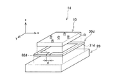
図1には、半導体装置1の要部分解図が模式的に示されている。図2〜図4は、半導体素子が実装基板に接合される工程を示す。図5は、実装基板に接合した半導体素子に発生する熱応力を示す斜視図である。図6では、半導体装置1の上面図と、半導体素子内の位置に対応する熱応力の分布を示す。
(First embodiment)
The semiconductor device 1 according to the first embodiment will be described below with reference to FIGS. The semiconductor device of the first embodiment is provided with a semiconductor element constituting a switching element or the like. And the tensile strength of the joining member which joins the peripheral part of a semiconductor element to a mounting substrate, and the joining member which joins the center part of a semiconductor element to a mounting board differ.
FIG. 1 schematically shows an exploded view of the main part of the semiconductor device 1. 2 to 4 show a process in which the semiconductor element is bonded to the mounting substrate. FIG. 5 is a perspective view showing thermal stress generated in the semiconductor element bonded to the mounting substrate. FIG. 6 shows a top view of the semiconductor device 1 and a distribution of thermal stress corresponding to the position in the semiconductor element.
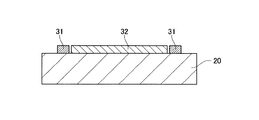
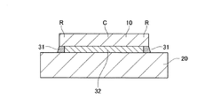
図1に示すように、半導体装置1では、上面略正方形の半導体素子10が接合層30によって実装基板20に接合されている。接合層30は、上面から見て、半導体素子10よりも若干大きい略正方形となっている。
本実施例の半導体素子10は、主にSi(シリコン)により構成されている。半導体素子10の中央部Cには、図示していないが、半導体素子10の主動作領域が配設されている。半導体素子10の四辺に隣接する周辺部Rには、電極パッド等が配設されている。
実装基板20は、主にCu(銅)又はAl(アルミニウム)等の熱伝導率の高い金属で構成されている。
接合層30は2種類の材料からなり、略正方形の四辺に沿って、枠形状の第1接合部材31が設けられている。第1接合部材31の中央の開口には、第2接合部材32が設けられている。第1接合部材31の引っ張り強度T1(Pa)は、第2接合部材32の引っ張り強度T2(Pa)よりも大きい(T1>T2)。第1接合部材31の引っ張り強度T1(Pa)は、200(MPa)以上であることが好ましい。第1接合部材31としては、AuSn,AuSi,AuGe等の材料が用いられる。第2接合部材32の引っ張り強度T2(Pa)は、10(MPa)以下であることが好ましい。第2接合部材32には、Ag系のエポキシ導電性接着材(Ag:85%〜90%、エポキシ:15%〜10%)等が用いられる。
As shown in FIG. 1, in the semiconductor device 1, the
The
The mounting
The
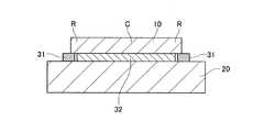
次に図2〜図4を用いて、半導体素子10を実装基板20に接合する工程を説明する。図2〜図4は、図1のII−II線に対応する半導体装置10の断面図である。
まず図2に示すように、実装基板20の上面に、枠形状の第1接合部材31と枠内に嵌まる第2接合部32を載置する。
次に図3に示すように、半導体素子10の中央部Cを第2接合部材32の上に配置するとともに、半導体素子10の周辺部Rを第1接合部材31の上に配置する。そして、温度を、第1接合部材31の融点と第2接合部材32の融点のいずれよりも高い温度にまで上昇させる。
すると図4に示すように、第1接合部材31と第2接合部材32は溶融する。その後に温度が下げられることによって、第1接合部材31と第2接合部材32は再び固化する。これにより、半導体素子10は接合層30によって実装基板20に接合(加熱接合)される。
Next, the process of joining the
First, as shown in FIG. 2, a frame-shaped first bonding
Next, as shown in FIG. 3, the central portion C of the
Then, as shown in FIG. 4, the first joining
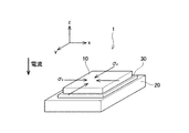
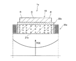
ここで、実装基板の線膨張係数をTCEsub、Siの線膨張係数をTCEsi、半導体素子を実装基板に実装する際の加熱温度をTpack、半導体装置の動作温度をTop、Siのヤング率をYsiとすると、図5に示す半導体素子10のx方向及び−x方向に発生する熱応力σxと、y方向及び−y方向に作用する熱応力σyの絶対値は、それぞれ(式1)によって算出される。
σx,σyの絶対値=ABS[(TCEsub−TCEsi)×(Tpack−Top)×Ysi]
・・・(式1)
Here, the linear expansion coefficient of the mounting substrate is TCE sub , the linear expansion coefficient of Si is TCE si , the heating temperature when mounting the semiconductor element on the mounting substrate is T pack , the operating temperature of the semiconductor device is T op , and the Si Young When the rate is Y si , the absolute values of the thermal stress σ x generated in the x direction and the −x direction and the thermal stress σ y acting in the y direction and the −y direction of the
Absolute value of σ x , σ y = ABS [(TCE sub −TCE si ) × (T pack −T op ) × Y si ]
... (Formula 1)
本実施例の実装基板20を構成している金属は、半導体素子10を構成しているSiよりも線膨張係数TCEが大きい(TCEsub>TCEsi)。この場合、熱応力σx,σyは負の値となり、図5に示すように、半導体素子10を中心方向に圧縮する圧縮応力が発生する。
なお、実際の半導体素子10では、接合層が一様な場合には、半導体素子の中心に近い程、機械的拘束力が強くなる。これに対応して、接合層が一様な場合には、図6の太い破線(σx2,σy2)で示すように、実際の熱応力の絶対値は、半導体素子10の中心に近い程大きくなる。
半導体素子に応力が発生すると、ピエゾ抵抗効果によって、応力の大きさに応じて半導体素子の電気抵抗率が変化することが知られている。
例えば図5に示すように、電流が−z方向に流れる半導体素子10(縦型半導体素子)の場合、熱応力σx,σyが発生すると、−z方向の電気抵抗率は、下記の(式2)に示す変化割合で変化する。
電気抵抗率が変化割合=[(ピエゾ抵抗係数53.4×10⁻¹¹)×(σx+σy)]
・・・(式2)
熱応力σx,σyが、図5、図6に示すような圧縮応力である場合(熱応力σx,σyが負の値となる場合)、熱応力σxと熱応力σyの絶対値が大きくなる程、−z方向の電気抵抗率は(式2)で算出される割合をもって小さくなる。したがって、接合層が一様な場合には、実際の電気抵抗率は、半導体素子の中心に近い程小さくなる。そこで、−z方向に流れる電流は、半導体素子の中央部に集中し、中央部が集中的に発熱する現象が生じる。
The metal constituting the mounting
In the
When stress is generated in a semiconductor element, it is known that the electrical resistivity of the semiconductor element changes according to the magnitude of the stress due to the piezoresistive effect.
For example, as shown in FIG. 5, in the case of the semiconductor element 10 (vertical semiconductor element) in which current flows in the −z direction, when thermal stresses σ x and σ y are generated, the electrical resistivity in the −z direction is It changes at the change rate shown in Equation 2).
Electric resistivity change rate = [(piezoresistance coefficient 53.4 × 10 −11 ) × (σ x + σ y )]
... (Formula 2)
When the thermal stresses σ x and σ y are compressive stresses as shown in FIGS. 5 and 6 (when the thermal stresses σ x and σ y are negative values), the thermal stress σ x and the thermal stress σ y As the absolute value increases, the electrical resistivity in the −z direction decreases with the ratio calculated by (Equation 2). Therefore, when the bonding layer is uniform, the actual electrical resistivity becomes smaller as it is closer to the center of the semiconductor element. Therefore, a current flowing in the −z direction is concentrated in the central portion of the semiconductor element, and a phenomenon occurs in which the central portion generates heat intensively.
一方、実施例1の半導体装置1を用いれば、半導体素子10の周辺部Rが、引っ張り強度の大きい第1接合部材31によって、実装基板20に強く拘束された状態となっている。これに対応して、図6の太い実線(σx1,σy1)で示すように、第1接合部材31によって実装基板20に接合されている領域(周辺部R)では、熱応力σx1,σy1の絶対値が半導体素子の中心に近づくほど大きくなっているものの、第2接合部材32によって実装基板20に接合されている領域(中央部C)では、熱応力σx1,σy1の絶対値が半導体素子内の位置に無関係にほぼ一定値に維持されている。
熱応力が分布していなければ、電気抵抗率も分布しない。したがって、半導体装置1を用いれば、半導体素子10内の中央部Cにおいて電気抵抗率が局所的に減少し、大電流が局所的に流れて局所的に発熱する現象の発生を抑制することができる。
On the other hand, when the semiconductor device 1 according to the first embodiment is used, the peripheral portion R of the
If the thermal stress is not distributed, the electrical resistivity is not distributed. Therefore, if the semiconductor device 1 is used, it is possible to suppress the occurrence of a phenomenon in which the electrical resistivity is locally reduced at the central portion C in the
前述したように、中央部Cに半導体素子10の主動作領域が配設されている。周辺部Rには、電極パッド等が配設されている。したがって、周辺部Rでは、その位置によって電気抵抗率が変化していても、半導体素子10の動作には影響が少ない。本実施例の半導体装置1によれば、半導体素子10の周辺部Rが集中的に拘束された状態で実装基板20に確実に接合されるとともに、中央部Cの機械的拘束力が弱められることで、中央部Cの中心に近づくほど発達していた熱応力が発達するのを抑制することができる。これにより、中央部Cでは、位置によって電気抵抗率が相違する度合いを低減することができる。したがって、半導体素子10がオン状態の際に、主動作領域の電気抵抗率が低い部分に電流が集中し、この部分が局所的に発熱するのを防止することができる。
As described above, the main operation region of the
(第2実施例)
次に第2実施例の半導体装置1aを図7、図8を参照して説明する。
半導体装置1aでは、半導体素子10の対向する二辺に隣接する範囲が集中的に拘束された状態で実装基板20に接合されている。
図7には、半導体装置1aの要部分解図が模式的に示されている。図8では、半導体装置1aの上面図と、半導体素子10内の位置に対応する熱応力の分布を示す。
(Second embodiment)
Next, a
In the
FIG. 7 schematically shows an essential part exploded view of the
図7に示すように、半導体装置1aでは、上面略正方形の半導体素子10が接合層30aによって実装基板20に接合されている。
本実施例の半導体素子10は、主にSi(シリコン)により構成されている。半導体素子10の中央部Caには、スイッチング素子等が配設され、半導体素子10の主動作領域が構成されている。半導体素子10の対向する二辺に隣接する周辺部Raには、電極パッド等が配設されている。本実施例の半導体素子10と実装基板20は、実施例1の半導体装置1と同様の構成であるので説明を省略し、図7,8中では同じ符号を用いている。
接合層30aは、半導体素子10のy方向に伸びる対向する二辺に沿って伸びるストライプ状の第1接合部材31aを備えている。第1接合部材31aの間には、第2接合部材32aが設けられている。第1接合部材31aの引っ張り強度T1(Pa)は、第2接合部材32aの引っ張り強度T2(Pa)よりも大きい(T1>T2)。
半導体装置1aについて、半導体素子10を実装基板20に接合する工程は、実装基板20に載置する接合層30aの構成が相違するだけで、あとは実施例1の半導体装置1と同様であるので、説明を省略する。
第1接合部材31aによって半導体素子10aの周辺部Raが実装基板20に接合される。また、第2接合部材32aによって半導体素子10aの中央部Caが実装基板20に接合される。
As shown in FIG. 7, in the
The
The
Regarding the
The peripheral portion Ra of the semiconductor element 10a is bonded to the mounting
実施例2の半導体装置1aを用いれば、半導体素子10は、引っ張り強度の大きい第1接合部材31aによって対向する二辺に隣接する周辺部Raが集中的に拘束された状態となっている。これに対応して、x方向及び−x方向では、図8の太い実線(σx1a)で示すように、第1接合部材31aによって実装基板20に接合されている領域(周辺部Ra)では、熱応力σx1aの絶対値が半導体素子の中心に近づくほど大きくなっているのに対し、第2接合部材32aによって実装基板20に接合されている領域(中央部Ca)では、熱応力σx1aの絶対値は半導体素子内の位置に無関係にほぼ一定値に維持されている。
また、x方向での中央部Caにおけるy方向に沿った断面では、半導体素子10aの周辺部Rzは第2接合部材32aで実装基板に接合されており、周辺部Rzで集中的に拘束されているわけでない。しかしながら、第2接合部材32aの引っ張り強度T2が低いので、図8の太い実線(σy1a)で示すように、大きな熱応力は発生しない。なお、周辺部Raにおけるy方向に沿った断面では、全てが第1接合部材31aで接合されており、強固に拘束されている。したがって、図8の太い破線(σy2)で示すような熱応力σy2が発生する。しかしながら、その部分は半導体素子10の主動作領域でなく、大きな熱応力が作用しても特段の問題は生じない。
図8に示す中央部Caのように、熱応力σx1aに変化がない部分では、電気抵抗率の変化はない。したがって、半導体装置1aを用いれば、半導体素子10aの中央部Ca内の位置によって電気抵抗率が分布する度合いを低減することができる。また、図8に示す中央部Caのように、y方向の熱応力(σy1a)が小さければ、電気抵抗率はほとんど変化しない。
If the
In the cross section along the y direction at the central portion Ca in the x direction, the peripheral portion Rz of the semiconductor element 10a is bonded to the mounting substrate by the
As in the central portion Ca shown in FIG. 8, there is no change in the electrical resistivity in the portion where the thermal stress σ x1a is not changed. Therefore, if the
図1の半導体装置1と図7の半導体装置1aは、z方向に電流が流れる縦型の半導体素子であるが、本発明は、図9に示すように、x方向に電流が流れる横型の半導体装置1bにも適用することができる。半導体装置1bの接合層30bは、半導体装置1aの接合層30aと同様に構成されている。接合層30bは、半導体素子のx方向に伸びる対向する二辺に沿って伸びるストライプ状の第1接合部材31bを備えている。第1接合部材31bの間には、第2接合部材32bが設けられている。半導体素子10bは、y方向の両端に位置する周辺部Rbが、集中的に拘束された状態となっている。これによって、y方向及び−y方向の熱応力σy1bが発生し、x方向及び−x方向の熱応力はほとんど発生しない。
The semiconductor device 1 in FIG. 1 and the
一般的に、接合層や実装基板が一様であれば、x方向とy方向に熱応力σx,σyが発生する。この応力によって、x方向の電気抵抗率が変化する割合が、下記の(式3)で算出される。
電気抵抗率が変化する割合=ピエゾ抵抗係数(−102.2×10⁻¹¹)×σx
+ピエゾ抵抗係数(53.4×10⁻¹¹)×σy・・・(式3)
これは、熱応力σxと熱応力σyが、図9に示すように圧縮応力である場合(熱応力σxとσyが負の値の場合)、熱応力σxの絶対値が大きくなる程、x方向の電気抵抗率は(式3)で算出される割合をもって大きくなることを示している。また、熱応力σyの絶対値が大きくなる程、x方向の電気抵抗率は、(式3)で算出される割合をもって小さくなることを示している。
In general, if the bonding layer and the mounting substrate are uniform, thermal stresses σ x and σ y are generated in the x and y directions. The rate at which the electrical resistivity in the x direction changes due to this stress is calculated by the following (Equation 3).
Ratio of change in electrical resistivity = piezoresistance coefficient (−102.2 × 10 −11 ) × σ x
+ Piezoresistance coefficient (53.4 × 10 −11 ) × σ y (Expression 3)
This is because when the thermal stress σ x and the thermal stress σ y are compressive stresses as shown in FIG. 9 (when the thermal stresses σ x and σ y are negative values), the absolute value of the thermal stress σ x is large. As shown, the electrical resistivity in the x direction increases with the ratio calculated by (Equation 3). Further, it is shown that the electrical resistivity in the x direction decreases with the ratio calculated by (Equation 3) as the absolute value of the thermal stress σ y increases.
半導体装置1bでは、図9に示すようにy方向の熱応力σy1bが、半導体素子10bを圧縮する方向に発生する。x方向の熱応力σx1bは小さい。
したがって、図9に示す半導体装置1bの場合には、下記式が得られる。
x方向の電気抵抗率が変化する割合=ピエゾ抵抗係数(53.4×10⁻¹¹)×σy1b
半導体装置1bでは、この割合をもって、熱応力σy1bの絶対値が大きくなる程、x方向の電気抵抗率が小さくなる。これにより、半導体装置1bは、周辺部Rbで確実に実装基板20に接合されているとともに、通電方向であるx方向の抵抗が大きくなることがなく、オン状態の際の損失が少ない。このように、半導体装置1bでは、一方向に発生する熱応力を積極的に利用している。
In the
Therefore, in the case of the
Ratio of change in electrical resistivity in x direction = piezoresistance coefficient (53.4 × 10 −11 ) × σ y1b
In the
また、本発明は、図10に示すようなx方向に電流が流れる横型の半導体装置1cにも適用することができる。半導体装置1cの接合層30cは、半導体装置1aの接合層30aと同様に構成されている。接合層30cは、半導体素子のy方向に伸びる対向する二辺に沿って伸びるストライプ状の第1接合部材31cを備えている。第1接合部材31cの間には、第2接合部材32cが設けられている。半導体素子10cは、x方向の両端に存在する周辺部Rcで、集中的に拘束された状態となっている。これによって、x方向及び−x方向の熱応力σx1cが発生し、y方向及び−y方向の熱応力はほとんど発生しない。
The present invention can also be applied to a
したがって、図10に示す半導体装置1cの場合には、下記式が得られる。
x方向の電気抵抗率が変化する割合=ピエゾ抵抗係数(−102.2×10⁻¹¹)×σx1c
半導体装置1cでは、この割合をもって、熱応力σx1cの絶対値が大きくなる程、x方向の電気抵抗率が大きくなる。これにより、半導体装置1cは、周辺部Rcで確実に実装基板20に接合されているとともに、通電方向であるx方向の抵抗が大きくなり、短絡負荷時の破壊耐量が高い。このように、半導体装置1cでは、一方向に発生する熱応力を積極的に利用している。
Therefore, in the case of the
Ratio of change in electric resistivity in x direction = piezoresistance coefficient (−102.2 × 10 −11 ) × σ x1c
In the
(第3実施例)
次に第3実施例の半導体装置1dを図11〜図18を参照して説明する。
半導体装置1dでは、半導体素子10の周辺部Rを実装基板20に接合する接合部材の融点と、半導体素子10の中央部Cを実装基板20に接合する接合部材の融点が相違している。
図11には、半導体装置1dの要部分解図が模式的に示されている。図12〜図17には、半導体素子が実装基板に接合される工程を示す。図18では、半導体装置1d内の位置に対応する電気抵抗率の分布を示す。
(Third embodiment)
Next, a
In the
FIG. 11 schematically shows an essential part exploded view of the semiconductor device 1d. 12 to 17 show a process in which the semiconductor element is bonded to the mounting substrate. FIG. 18 shows a distribution of electrical resistivity corresponding to a position in the
図11に示すように、半導体装置1dには、上面略正方形の半導体素子10が接合層30dによって実装基板20に接合されている。接合層30dは、上面から見て、半導体素子10よりも若干大きい略正方形となっている。
本実施例の半導体素子10、実装基板20は、第1実施例の半導体装置1と同様であるので、説明を省略する。
接合層30dには、略枠状であるとともに、1辺に間隔dの開口部を有する第3接合部材31dが設けられている。第3接合部材31dの中央部には、第4接合部材32dが設けられている。第3接合部材31dの融点Tm1(℃)は、第4接合部材32dの融点Tm2(℃)よりも高い(Tm1(℃)>Tm2(℃))。第3接合部材31dには、AuSn,AuSi,AuGe等の部材が用いられる。第4接合部材32dには、SnAg,PbSn(Pbは50パーセント以下),SnCu,SnIn,SnBi等の部材が用いられる。
As shown in FIG. 11, in the
Since the
The
次に、図12〜図17を用いて、半導体素子10を実装基板20に接合する工程を説明する。
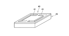
図12に示すように、まず、実装基板20の上面にソルダーレジスト40をパターンニングして配設する。ソルダーレジスト40は、第3接合部材31dと第4接合部材32dと同じ厚みか、あるいはそれ以上の厚み(図12に示す上下方向の寸法)に形成する。ソルダーレジスト40には、第3接合部材31dの形状に対応する溝41が設けられている。
次に、図13に示すように、溝41に第3接合部材31dを配置する。第3接合部材31dには、間隔dのゲートGが設けられている。そして、その上に半導体素子10を載置する。
この状態で、第3接合部材31dの融点よりも高い温度にまで加熱し、図14に示すように、半導体素子10を実装基板20に加熱接合する。
次に図15に示すように、ソルダーレジスト40を除去する。これにより、第4接合部材32dの溶融材料が注入される中空部が形成されるとともに、第4接合部材32dの溶融材料を注入可能なゲートG(幅d)が形成される。
そして図16に示すように、ゲートGから、第4接合部材32dの融点よりも高い温度にまで加熱することで溶融させた第4接合部材32dを注入する。溶融材料は毛細管現象によって中空部に広がる。その後温度を下げることによって、第4接合部材32dが固化する。以上によって熱接合が完成する。
Next, the process of joining the
As shown in FIG. 12, first, a solder resist 40 is patterned and disposed on the upper surface of the mounting
Next, as shown in FIG. 13, the
In this state, heating is performed to a temperature higher than the melting point of the
Next, as shown in FIG. 15, the solder resist 40 is removed. Thereby, a hollow portion into which the molten material of the
Then, as shown in FIG. 16, the
ここで、実装基板の線膨張係数をTCEsub、Siの線膨張係数をTCEsi、第3接合部材31dの融点をTm1、第4接合部材32dの融点をTm2、半導体装置の動作時の温度をTop(20℃〜30℃程度)、Siのヤング率をYsiとすると、第3接合部材31dにより接合された周辺部R(4辺の周辺)に作用する熱応力σ1、第4接合部材32dにより接合された中央部Cに作用する熱応力σ2の絶対値は、それぞれ下記(式4)によって算出される。熱応力σ1及び熱応力σ2は、半導体素子10を圧縮する方向に発生する。
熱応力σiの絶対値=ABS[(TCEsub−TCEsi)×(Tmi−Top)×Ysi]
ここで、iは1または2である (式4)
前述したように、融点Tm1(℃)>融点Tm2(℃)であるので、(式4)より、熱応力σ1の絶対値>熱応力σ2の絶対値となる。したがって、接合層30dを、一様に第3接合部材31dによって形成した場合と比較して、半導体素子10の中央部Cに発生する熱応力の絶対値を低減することができる。
Here, the linear expansion coefficient of the mounting substrate is TCE sub , the linear expansion coefficient of Si is TCE si , the melting point of the
Absolute value of thermal stress σ i = ABS [(TCE sub −TCE si ) × (T m i−T op ) × Y si ]
Here, i is 1 or 2 (Formula 4)
As described above, since melting point Tm1 (° C.)> Melting point Tm2 (° C.), from Equation 4, the absolute value of thermal stress σ 1 > the absolute value of thermal stress σ 2 . Therefore, the absolute value of the thermal stress generated in the central portion C of the
半導体素子10は、−z方向に電流が流れる縦型半導体素子であるので、熱応力σ1,σ2が発生すると、−z方向の電気抵抗率が変化する。その割合が、(式5)で算出される。
−z方向の電気抵抗率が変化する割合=[(ピエゾ抵抗係数53.4×10⁻¹¹)×σi]
ここで、iは1または2である (式5)
これにより、熱応力σ1の絶対値>熱応力σ2の絶対値の場合、図18に示すように、中央部Cの電気抵抗率の変化を低減することができる。
Since the
Ratio of change in electrical resistivity in −z direction = [(piezoresistance coefficient 53.4 × 10 −11 ) × σ i ]
Here, i is 1 or 2 (Formula 5)
Thereby, when the absolute value of the thermal stress σ 1 > the absolute value of the thermal stress σ 2 , as shown in FIG. 18, the change in the electrical resistivity of the central portion C can be reduced.
このように、第3実施例の半導体装置1dを用いれば、半導体素子10の中央部C内の位置による電気抵抗率の変化の度合いを低減することができる。したがって、半導体素子10がオン状態の際に、主動作領域の電気抵抗率が低い部分に電流が集中し、この部分が局所的に発熱するのを防止することができる。
Thus, if the
第3実施例では、接合層30dに、融点が相違する2種類の接合部材、すなわち第3接合部材31dと第4接合部材32dが設けられている場合について説明した。接合層には、融点が相違する3種類以上の接合部材が設けられていてもよい。例えば、接合層に3種類の接合部材が設けられている場合、図11に示す接合層30dのように二重ではなく、三重(最周辺部対応領域、周辺部対応領域、中央部対応領域)に構成される。そして、外側ほど融点が高い材料で接合部材が形成される。この構成によれば、半導体素子10が接合層によって実装基板20に接合される際の機械的拘束力(クランプ力)、及び半導体素子10に発生する熱応力の大きさの両者を満足する値に調整し易い。
In the third embodiment, the case where the
(第4実施例)
次に第4実施例の半導体装置1eを図19を参照して説明する。
半導体装置1eでは、半導体素子10の周辺部Rが接合される実装基板の領域(周辺部対応領域)の線膨張係数が、中央部Cが接合される実装基板の領域(中央部対応領域)の線膨張係数と相違する。
図19には、半導体装置1eの要部断面図と、実装基板20eの位置に対応する線膨張係数TCEの分布を示す。
(Fourth embodiment)
Next, a
In the
FIG. 19 shows a cross-sectional view of the main part of the
図19に示すように、半導体装置1eには、上面略正方形の半導体素子10が実装基板20eに接合層30eで接合されている。接合層30eは、上面から見て、半導体素子10よりも若干大きく形成されている。
本実施例の半導体素子10は、第1実施例と同様であるので、説明を省略する。本実施例の接合層30eは、一様な部材で形成されている。
実装基板20eは、周辺部R側ほど、多数の孔21eが形成された多孔体の孔21eに多孔体と異なる材料を含浸させた材料で構成されている。含浸させた材料は多孔体の材料よりも、線膨張係数が大きい。多孔体の材料には、タングステン、Mo,SiC等が用いられる。多孔体の孔21eに含浸させる材料には、Cu,Al等が用いられる。多孔体に設ける孔21eの数は、作業温度や、冷却条件、雰囲気等により制御可能であることが知られている。この実施例では、2種類の材料を組み合わせて用いる点では、半導体素子の周辺部に接合している領域と半導体素子の中央部に接合している領域とで異ならない。ただし、組成比が相違する。これもまた、半導体素子の周辺部に接合している領域と半導体素子の中央部に接合している領域とで材料組成が異なることに相当する。
As shown in FIG. 19, in the
Since the
The mounting
一般的に、一様な実装基板に一様な接合層で接合された半導体素子には、半導体素子の中心に近い程熱応力による影響が大きくなる。本実施例の半導体装置1eでは、周辺部対応領域と中央部対応領域とで、単位体積あたりの実装基板に配設する材料(多孔体の材料よりも線膨張係数の大きい)の量を異ならせることによって、周辺部対応領域の線膨張係数の方が中央部対応領域の線膨張係数よりも大きくなるように構成している。
この実施例では、半導体素子10の周辺部R側を接合する領域ほど、実装基板20eの線膨張係数が大きい。したがって、周辺部R側と比較して中央部Cの方が機械的拘束力が小さく、周辺部Rで集中的にクランプされた状態となって実装基板20eに接合されている。これにより、半導体素子10の中央部C内の位置による熱応力の変化の度合いを低減することができる。熱応力の変化の度合いが低減されれば、電気抵抗率の変化の度合いも低減される。したがって、半導体装置1eを用いれば、半導体素子10内の位置による電気抵抗率の相違を低減することができる。
また、第4実施例の半導体装置1eによれば、実装基板の周辺部対応領域と中央部対応領域の線膨張係数を簡単に調節することができる。
In general, a semiconductor element bonded to a uniform mounting substrate with a uniform bonding layer is more affected by thermal stress as it is closer to the center of the semiconductor element. In the
In this embodiment, the linear expansion coefficient of the mounting
Moreover, according to the
第4実施例では、単位体積あたりの実装基板20eに空けられている同じ大きさの孔21eの数が、中央部対応領域よりも周辺部対応領域の方が多く、全ての孔21eに実装基板20eよりも大きい線膨張係数を有する材料を含浸する場合について説明した。周辺部対応領域の線膨張係数を中央部対応領域の線膨張係数よりも大きくする構成は本実施例に限定されるものではない。
例えば、単位体積あたりの実装基板に空けられている同じ大きさの孔の数は、中央部対応領域も周辺部対応領域も同じであって、孔に選択的に実装基板よりも大きい線膨張係数を有する材料を配設してもよい。この場合、中央部対応領域に設けられている孔よりも周辺部対応領域に設けられている孔に多くの材料を含浸する。あるいは、単位体積あたりの実装基板に空けられている孔の数は同じであって、周辺部対応領域では中央部対応領域よりも大きい孔が設けられていてもよい。
また、多孔質の実装基板の孔に、実装基板よりも小さい線膨張係数を有する材料を配設する場合としては以下の構成が考えられる。
例えば、単位体積あたりの実装基板に空けられている同じ大きさの孔の数が、周辺部対応領域よりも中央部対応領域の方が多く、全ての孔に実装基板よりも小さい線膨張係数を有する材料を含浸する。あるいは、単位体積あたりの実装基板に空けられている孔の数と大きさは同じであって、孔に選択的に実装基板よりも小さい線膨張係数を有する材料を配設してもよい。この場合、周辺部対応領域に設けられている孔よりも中央部対応領域に設けられている孔に多くの材料を含浸する。あるいは、単位体積あたりの実装基板に空けられている孔の数は同じであって、中央部対応領域では周辺部対応領域よりも大きい孔が設けられていてもよい。
これらによって、周辺部対応領域の線膨張係数の方が中央部対応領域の線膨張係数よりも大きくなるように構成することができる。
In the fourth embodiment, the number of
For example, the number of holes of the same size vacated in the mounting board per unit volume is the same in both the central area and the peripheral area, and the linear expansion coefficient is selectively larger than the mounting board. You may arrange | position the material which has these. In this case, more material is impregnated in the hole provided in the peripheral area corresponding region than in the hole provided in the central area. Alternatively, the number of holes vacated in the mounting substrate per unit volume may be the same, and the peripheral part corresponding region may be provided with a larger hole than the central part corresponding region.
Further, the following configuration is conceivable when a material having a smaller linear expansion coefficient than that of the mounting substrate is disposed in the hole of the porous mounting substrate.
For example, the number of holes of the same size per unit volume that are vacated in the mounting board is larger in the center area than in the peripheral area, and all holes have a smaller linear expansion coefficient than the mounting board. Impregnated with material. Alternatively, the number and size of the holes vacated in the mounting substrate per unit volume may be the same, and a material having a smaller linear expansion coefficient than the mounting substrate may be selectively disposed in the hole. In this case, a larger amount of material is impregnated into the hole provided in the center corresponding region than the hole provided in the peripheral corresponding region. Alternatively, the number of holes vacated in the mounting substrate per unit volume may be the same, and a larger hole may be provided in the center corresponding region than in the peripheral corresponding region.
Accordingly, the linear expansion coefficient in the peripheral corresponding region can be configured to be larger than the linear expansion coefficient in the central corresponding region.
また、図20に示すように、線膨張係数の大きい材料と線膨張係数の小さい材料を貼り合わせることで、実装基板を形成してもよい。
図20に示す実装基板20fでは、母材22fに、半導体素子10の中心が接合される領域程深く形成した上面開口の穴を設ける。そして、この穴に母材22fよりも線膨張係数の小さい材料で形成されているとともに穴を埋める形状の部材23fを、ろう付け等で張り合わせる。母材22fとしては、Cu,Al等が用いられる。部材23fとしては、W,Mo等が用いられる。このように構成された実装基板20fは、図19に示した実装基板20eと同様、半導体素子10の周辺部対応領域ほど線膨張係数が大きい。したがって、実装基板20eと同様、半導体素子10中央部の位置による熱応力の変化を低減することができる。また、母体である多孔体の孔に材料を含浸させる方法と比較して、母体の構成、及び製造方法が簡単であるので、製造コストを抑制することができる。
また、図21に示す実装基板20gでは、母材22gに、半導体素子10の中心が接合される領域程深く形成した上面開口の階段上の穴を設ける。そして、この穴に母材22gよりも線膨張係数の小さい材料で形成されているとともに穴を埋める形状の部材23gを張り合わせる。母材22gとしては、Cu,Al等が用いられる。部材23gとしては、W,Mo等が用いられる。このように構成された実装基板20gは、図19に示した実装基板20eと同様、半導体素子10の周辺部対応領域ほど線膨張係数が大きい。したがって、実装基板20eと同様、半導体素子10中央部の位置による熱応力の変化を低減することができる。また、母体である多孔体の孔に材料を含浸させる方法と比較して、母体の構成、及び製造方法が簡単であるので、製造コストを抑制することができる。
以上の実施例では、2種類の材料を張り合わせて用いる点では、半導体素子の周辺部に接合している領域と半導体素子の中央部に接合している領域とで異ならない。ただし、厚み(それが組成比となる)が相違する。これもまた、半導体素子の周辺部に接合している領域と半導体素子の中央部に接合している領域とで材料組成が異なることに相当する。
Further, as shown in FIG. 20, the mounting substrate may be formed by bonding a material having a large linear expansion coefficient and a material having a small linear expansion coefficient.
In the mounting
Further, in the mounting
In the above-described embodiments, the two types of materials are used together, and the region bonded to the peripheral portion of the semiconductor element is not different from the region bonded to the central portion of the semiconductor element. However, the thickness (which is the composition ratio) is different. This also corresponds to the difference in material composition between the region bonded to the peripheral portion of the semiconductor element and the region bonded to the central portion of the semiconductor element.
また、第1実施例〜第4実施例では、半導体素子が上面略正方形である場合について説明した。本発明は、半導体素子が上面略長方形等、他の形状の半導体素子が設けられた半導体装置についても適用することができる。例えば、半導体素子が上面略長方形の形状である場合、対向する短辺の周りを集中的にクランプするように構成すれば、四辺の周りや対向する長辺の周りを集中的にクランプする場合と比較して、機械的拘束力が弱まるとともに、半導体素子に発生する熱応力が低減する。一方、対向する長辺の周りを集中的にクランプするように構成すれば、四辺の周りを集中的にクランプする場合と比較して、機械的拘束力が弱まるとともに半導体素子に発生する熱応力が低減するが、対向する短辺の周りを集中的にクランプする場合と比較すれば、機械的拘束力が強く半導体素子に発生する熱応力が大きい。
このように、不均一な接合層や不均一な実装基板を用いて、半導体素子を集中的にクランプする領域の位置や面積等を調節することで、半導体素子の機械的拘束力、半導体素子に発生する熱応力、半導体素子の電気抵抗率等を調節することができる。
In the first to fourth embodiments, the case where the semiconductor element has a substantially square top surface has been described. The present invention can also be applied to a semiconductor device in which a semiconductor element is provided with a semiconductor element having another shape such as a substantially rectangular top surface. For example, when the semiconductor element has a substantially rectangular shape on the upper surface, if it is configured to intensively clamp around the short sides facing each other, it may be clamped around the four sides or around the long sides facing each other. In comparison, the mechanical restraining force is weakened, and the thermal stress generated in the semiconductor element is reduced. On the other hand, if it is configured to intensively clamp around the opposite long sides, the mechanical restraining force is weakened and the thermal stress generated in the semiconductor element is reduced compared to the case of intensively clamping around the four sides. Although it is reduced, the mechanical restraint force is stronger and the thermal stress generated in the semiconductor element is larger than in the case of intensive clamping around the opposing short sides.
In this way, by using a non-uniform bonding layer or a non-uniform mounting substrate and adjusting the position and area of the region where the semiconductor element is clamped intensively, the mechanical restraining force of the semiconductor element can be reduced. The generated thermal stress, the electrical resistivity of the semiconductor element, and the like can be adjusted.
以上、本発明の具体例を詳細に説明したが、これらは例示にすぎず、特許請求の範囲を限定するものではない。特許請求の範囲に記載の技術には、以上に例示した具体例を様々に変形、変更したものが含まれる。
また、本明細書または図面に説明した技術要素は、単独であるいは各種の組合せによって技術的有用性を発揮するものであり、出願時の請求項記載の組合せに限定されるものではない。また、本明細書または図面に例示した技術は複数目的を同時に達成するものであり、そのうちの一つの目的を達成すること自体で技術的有用性を持つものである。
Specific examples of the present invention have been described in detail above, but these are merely examples and do not limit the scope of the claims. The technology described in the claims includes various modifications and changes of the specific examples illustrated above.
In addition, the technical elements described in the present specification or drawings exhibit technical usefulness alone or in various combinations, and are not limited to the combinations described in the claims at the time of filing. In addition, the technology illustrated in the present specification or the drawings achieves a plurality of objects at the same time, and has technical utility by achieving one of the objects.
1,1a,1b,1c,1d,1e,1f,1g 半導体装置
10,10a 半導体素子
20,20e,20f,20g 実装基板
21e 孔
22f,22g 母材
23f,23g 部材
30,30a,30b,30c,30d,30e 接合層
31,31a,31b,31c 第1接合部材
32,32a,32b,32c 第2接合部材
31d 第3接合部材
32d 第4接合部材
40 ソルダーレジスト
C,Ca,Cb 中央部
G ゲート
R,Ra、Rb 周辺部
1, 1a, 1b, 1c, 1d, 1e, 1f,
Claims (5)
接合層と実装基板の少なくとも一方は、半導体素子の周辺部に接合している領域と半導体素子の中央部に接合している領域とで、材料組成が異なっていることを特徴とする半導体装置。 A semiconductor device in which a semiconductor element is bonded to a mounting substrate by a bonding layer,
At least one of the bonding layer and the mounting substrate has a material composition different between a region bonded to the peripheral portion of the semiconductor element and a region bonded to the central portion of the semiconductor element.
Priority Applications (1)
| Application Number | Priority Date | Filing Date | Title |
|---|---|---|---|
| JP2006020221A JP2007201314A (en) | 2006-01-30 | 2006-01-30 | Semiconductor device |
Applications Claiming Priority (1)
| Application Number | Priority Date | Filing Date | Title |
|---|---|---|---|
| JP2006020221A JP2007201314A (en) | 2006-01-30 | 2006-01-30 | Semiconductor device |
Publications (1)
| Publication Number | Publication Date |
|---|---|
| JP2007201314A true JP2007201314A (en) | 2007-08-09 |
Family
ID=38455569
Family Applications (1)
| Application Number | Title | Priority Date | Filing Date |
|---|---|---|---|
| JP2006020221A Pending JP2007201314A (en) | 2006-01-30 | 2006-01-30 | Semiconductor device |
Country Status (1)
| Country | Link |
|---|---|
| JP (1) | JP2007201314A (en) |
Cited By (5)
| Publication number | Priority date | Publication date | Assignee | Title |
|---|---|---|---|---|
| JP2008277335A (en) * | 2007-04-25 | 2008-11-13 | Fuji Electric Device Technology Co Ltd | Semiconductor device and its manufacturing process |
| JP2012004171A (en) * | 2010-06-14 | 2012-01-05 | Nissan Motor Co Ltd | Semiconductor device |
| WO2012081167A1 (en) * | 2010-12-15 | 2012-06-21 | 日立オートモティブシステムズ株式会社 | Semiconductor device and method for manufacturing same |
| CN102646650A (en) * | 2011-02-22 | 2012-08-22 | 富士通株式会社 | Semiconductor device and method for manufacturing semiconductor device |
| US20160064350A1 (en) * | 2012-02-09 | 2016-03-03 | Robert Bosch Gmbh | Connection arrangement of an electric and/or electronic component |
Citations (6)
| Publication number | Priority date | Publication date | Assignee | Title |
|---|---|---|---|---|
| JPH06326141A (en) * | 1993-05-17 | 1994-11-25 | Mitsubishi Electric Corp | Base material for semiconductor-chip bonding and solder material for semiconductor-chip bonding as well as manufacture of solder material for semiconductor-chip bonding |
| WO1998043288A1 (en) * | 1997-03-24 | 1998-10-01 | Seiko Epson Corporation | Semiconductor device and method for manufacturing the same |
| JP2002299522A (en) * | 2002-03-28 | 2002-10-11 | Mitsubishi Electric Corp | Semiconductor device |
| JP2005050886A (en) * | 2003-07-29 | 2005-02-24 | Kyocera Corp | Compound substrate and its manufacturing method |
| JP2007044699A (en) * | 2005-08-05 | 2007-02-22 | Nissan Motor Co Ltd | Joined structure |
| JP2007110001A (en) * | 2005-10-17 | 2007-04-26 | Fuji Electric Holdings Co Ltd | Semiconductor device |
-
2006
- 2006-01-30 JP JP2006020221A patent/JP2007201314A/en active Pending
Patent Citations (6)
| Publication number | Priority date | Publication date | Assignee | Title |
|---|---|---|---|---|
| JPH06326141A (en) * | 1993-05-17 | 1994-11-25 | Mitsubishi Electric Corp | Base material for semiconductor-chip bonding and solder material for semiconductor-chip bonding as well as manufacture of solder material for semiconductor-chip bonding |
| WO1998043288A1 (en) * | 1997-03-24 | 1998-10-01 | Seiko Epson Corporation | Semiconductor device and method for manufacturing the same |
| JP2002299522A (en) * | 2002-03-28 | 2002-10-11 | Mitsubishi Electric Corp | Semiconductor device |
| JP2005050886A (en) * | 2003-07-29 | 2005-02-24 | Kyocera Corp | Compound substrate and its manufacturing method |
| JP2007044699A (en) * | 2005-08-05 | 2007-02-22 | Nissan Motor Co Ltd | Joined structure |
| JP2007110001A (en) * | 2005-10-17 | 2007-04-26 | Fuji Electric Holdings Co Ltd | Semiconductor device |
Cited By (5)
| Publication number | Priority date | Publication date | Assignee | Title |
|---|---|---|---|---|
| JP2008277335A (en) * | 2007-04-25 | 2008-11-13 | Fuji Electric Device Technology Co Ltd | Semiconductor device and its manufacturing process |
| JP2012004171A (en) * | 2010-06-14 | 2012-01-05 | Nissan Motor Co Ltd | Semiconductor device |
| WO2012081167A1 (en) * | 2010-12-15 | 2012-06-21 | 日立オートモティブシステムズ株式会社 | Semiconductor device and method for manufacturing same |
| CN102646650A (en) * | 2011-02-22 | 2012-08-22 | 富士通株式会社 | Semiconductor device and method for manufacturing semiconductor device |
| US20160064350A1 (en) * | 2012-02-09 | 2016-03-03 | Robert Bosch Gmbh | Connection arrangement of an electric and/or electronic component |
Similar Documents
| Publication | Publication Date | Title |
|---|---|---|
| US7489026B2 (en) | Methods and apparatus for a Quad Flat No-Lead (QFN) package | |
| US6753596B1 (en) | Resin-sealed semiconductor device | |
| JP2015050347A (en) | Semiconductor device and manufacturing method of the same | |
| JP2007201314A (en) | Semiconductor device | |
| JP7238277B2 (en) | Semiconductor device, lead frame and method for manufacturing semiconductor device | |
| JP2011142172A (en) | Power semiconductor device | |
| JP2005260181A (en) | Resin-sealed semiconductor device and manufacturing method thereof | |
| JP2007088030A (en) | Semiconductor device | |
| JP2018026417A (en) | Power semiconductor device | |
| JP2014143351A (en) | Manufacturing method of substrate for power module with heat sink | |
| WO2018070343A1 (en) | Semiconductor device | |
| JP5301497B2 (en) | Semiconductor device | |
| JP6551432B2 (en) | Semiconductor device and method of manufacturing the same | |
| WO2016042903A1 (en) | Semiconductor module | |
| JP2012069703A (en) | Semiconductor module and method for manufacturing semiconductor module | |
| JP2810285B2 (en) | Semiconductor device and manufacturing method thereof | |
| JP2014187245A (en) | Semiconductor device and method of manufacturing semiconductor device | |
| JP2008294282A (en) | Semiconductor device and method of manufacturing semiconductor device | |
| US9704775B2 (en) | Method for manufacturing thermal interface sheet | |
| JP7400293B2 (en) | Semiconductor device and semiconductor device manufacturing method | |
| JP7490974B2 (en) | Semiconductor module and method for manufacturing the same | |
| JP2004022964A (en) | Al-SiC COMPOSITE BODY, HEAT SINK COMPONENT USING THE SAME, AND SEMICONDUCTOR MODULE DEVICE | |
| JP2004327711A (en) | Semiconductor module | |
| JP2009105251A (en) | Solder film thickness control method, and circuit device | |
| JP5145168B2 (en) | Semiconductor device |
Legal Events
| Date | Code | Title | Description |
|---|---|---|---|
| A621 | Written request for application examination |
Free format text: JAPANESE INTERMEDIATE CODE: A621 Effective date: 20080613 |
|
| A977 | Report on retrieval |
Free format text: JAPANESE INTERMEDIATE CODE: A971007 Effective date: 20101006 |
|
| A131 | Notification of reasons for refusal |
Free format text: JAPANESE INTERMEDIATE CODE: A131 Effective date: 20101109 |
|
| A02 | Decision of refusal |
Free format text: JAPANESE INTERMEDIATE CODE: A02 Effective date: 20110419 |