JP2007200976A - Method for manufacturing semiconductor device - Google Patents
Method for manufacturing semiconductor device Download PDFInfo
- Publication number
- JP2007200976A JP2007200976A JP2006015004A JP2006015004A JP2007200976A JP 2007200976 A JP2007200976 A JP 2007200976A JP 2006015004 A JP2006015004 A JP 2006015004A JP 2006015004 A JP2006015004 A JP 2006015004A JP 2007200976 A JP2007200976 A JP 2007200976A
- Authority
- JP
- Japan
- Prior art keywords
- film
- insulating film
- fluorine
- forming
- gate electrode
- Prior art date
- Legal status (The legal status is an assumption and is not a legal conclusion. Google has not performed a legal analysis and makes no representation as to the accuracy of the status listed.)
- Pending
Links
- 239000004065 semiconductor Substances 0.000 title claims abstract description 182
- 238000004519 manufacturing process Methods 0.000 title claims description 57
- 238000000034 method Methods 0.000 title claims description 54
- YCKRFDGAMUMZLT-UHFFFAOYSA-N Fluorine atom Chemical compound [F] YCKRFDGAMUMZLT-UHFFFAOYSA-N 0.000 claims abstract description 191
- 229910052731 fluorine Inorganic materials 0.000 claims abstract description 191
- 239000011737 fluorine Substances 0.000 claims abstract description 191
- 239000000758 substrate Substances 0.000 claims abstract description 147
- 238000010438 heat treatment Methods 0.000 claims abstract description 31
- 230000015572 biosynthetic process Effects 0.000 claims description 111
- 238000009413 insulation Methods 0.000 claims description 9
- 238000000059 patterning Methods 0.000 claims description 6
- 238000009792 diffusion process Methods 0.000 abstract description 27
- 230000002093 peripheral effect Effects 0.000 description 83
- 229910021420 polycrystalline silicon Inorganic materials 0.000 description 48
- 229910052751 metal Inorganic materials 0.000 description 19
- 239000002184 metal Substances 0.000 description 19
- 238000005229 chemical vapour deposition Methods 0.000 description 16
- 239000010410 layer Substances 0.000 description 13
- VYPSYNLAJGMNEJ-UHFFFAOYSA-N Silicium dioxide Chemical compound O=[Si]=O VYPSYNLAJGMNEJ-UHFFFAOYSA-N 0.000 description 12
- 230000015556 catabolic process Effects 0.000 description 12
- 238000006731 degradation reaction Methods 0.000 description 12
- 239000012535 impurity Substances 0.000 description 12
- 229910052814 silicon oxide Inorganic materials 0.000 description 12
- 238000000206 photolithography Methods 0.000 description 10
- 229910052581 Si3N4 Inorganic materials 0.000 description 9
- 230000006866 deterioration Effects 0.000 description 9
- 239000011229 interlayer Substances 0.000 description 9
- HQVNEWCFYHHQES-UHFFFAOYSA-N silicon nitride Chemical compound N12[Si]34N5[Si]62N3[Si]51N64 HQVNEWCFYHHQES-UHFFFAOYSA-N 0.000 description 9
- 238000005530 etching Methods 0.000 description 8
- 229920005591 polysilicon Polymers 0.000 description 8
- 238000005468 ion implantation Methods 0.000 description 7
- 229910021332 silicide Inorganic materials 0.000 description 7
- FVBUAEGBCNSCDD-UHFFFAOYSA-N silicide(4-) Chemical compound [Si-4] FVBUAEGBCNSCDD-UHFFFAOYSA-N 0.000 description 7
- IJGRMHOSHXDMSA-UHFFFAOYSA-N Atomic nitrogen Chemical compound N#N IJGRMHOSHXDMSA-UHFFFAOYSA-N 0.000 description 6
- 238000000137 annealing Methods 0.000 description 6
- 230000004888 barrier function Effects 0.000 description 6
- 229910052739 hydrogen Inorganic materials 0.000 description 6
- 239000001257 hydrogen Substances 0.000 description 6
- 238000002955 isolation Methods 0.000 description 6
- UFHFLCQGNIYNRP-UHFFFAOYSA-N Hydrogen Chemical compound [H][H] UFHFLCQGNIYNRP-UHFFFAOYSA-N 0.000 description 5
- XUIMIQQOPSSXEZ-UHFFFAOYSA-N Silicon Chemical group [Si] XUIMIQQOPSSXEZ-UHFFFAOYSA-N 0.000 description 5
- 229910052710 silicon Inorganic materials 0.000 description 5
- ZOXJGFHDIHLPTG-UHFFFAOYSA-N Boron Chemical compound [B] ZOXJGFHDIHLPTG-UHFFFAOYSA-N 0.000 description 4
- 229910052796 boron Inorganic materials 0.000 description 4
- 230000002542 deteriorative effect Effects 0.000 description 4
- 230000003647 oxidation Effects 0.000 description 4
- 238000007254 oxidation reaction Methods 0.000 description 4
- 239000010703 silicon Substances 0.000 description 4
- OAICVXFJPJFONN-UHFFFAOYSA-N Phosphorus Chemical compound [P] OAICVXFJPJFONN-UHFFFAOYSA-N 0.000 description 3
- ATJFFYVFTNAWJD-UHFFFAOYSA-N Tin Chemical compound [Sn] ATJFFYVFTNAWJD-UHFFFAOYSA-N 0.000 description 3
- 229910021419 crystalline silicon Inorganic materials 0.000 description 3
- 238000001312 dry etching Methods 0.000 description 3
- 230000000694 effects Effects 0.000 description 3
- 229910052757 nitrogen Inorganic materials 0.000 description 3
- 229910052698 phosphorus Inorganic materials 0.000 description 3
- 239000011574 phosphorus Substances 0.000 description 3
- 238000004544 sputter deposition Methods 0.000 description 3
- WFKWXMTUELFFGS-UHFFFAOYSA-N tungsten Chemical compound [W] WFKWXMTUELFFGS-UHFFFAOYSA-N 0.000 description 3
- 229910052721 tungsten Inorganic materials 0.000 description 3
- 239000010937 tungsten Substances 0.000 description 3
- 238000001039 wet etching Methods 0.000 description 3
- 229910004298 SiO 2 Inorganic materials 0.000 description 2
- 229910008284 Si—F Inorganic materials 0.000 description 2
- 238000007796 conventional method Methods 0.000 description 2
- 230000007423 decrease Effects 0.000 description 2
- 238000010586 diagram Methods 0.000 description 2
- 230000005684 electric field Effects 0.000 description 1
- 150000002431 hydrogen Chemical class 0.000 description 1
- 238000002513 implantation Methods 0.000 description 1
- 230000010354 integration Effects 0.000 description 1
- 239000000463 material Substances 0.000 description 1
- 238000001020 plasma etching Methods 0.000 description 1
- 239000005368 silicate glass Substances 0.000 description 1
- 150000004760 silicates Chemical class 0.000 description 1
Images


Classifications
-
- H—ELECTRICITY
- H01—ELECTRIC ELEMENTS
- H01L—SEMICONDUCTOR DEVICES NOT COVERED BY CLASS H10
- H01L21/00—Processes or apparatus adapted for the manufacture or treatment of semiconductor or solid state devices or of parts thereof
- H01L21/02—Manufacture or treatment of semiconductor devices or of parts thereof
- H01L21/04—Manufacture or treatment of semiconductor devices or of parts thereof the devices having at least one potential-jump barrier or surface barrier, e.g. PN junction, depletion layer or carrier concentration layer
- H01L21/18—Manufacture or treatment of semiconductor devices or of parts thereof the devices having at least one potential-jump barrier or surface barrier, e.g. PN junction, depletion layer or carrier concentration layer the devices having semiconductor bodies comprising elements of Group IV of the Periodic System or AIIIBV compounds with or without impurities, e.g. doping materials
- H01L21/26—Bombardment with radiation
- H01L21/263—Bombardment with radiation with high-energy radiation
- H01L21/265—Bombardment with radiation with high-energy radiation producing ion implantation
- H01L21/26506—Bombardment with radiation with high-energy radiation producing ion implantation in group IV semiconductors
- H01L21/26513—Bombardment with radiation with high-energy radiation producing ion implantation in group IV semiconductors of electrically active species
-
- H—ELECTRICITY
- H01—ELECTRIC ELEMENTS
- H01L—SEMICONDUCTOR DEVICES NOT COVERED BY CLASS H10
- H01L21/00—Processes or apparatus adapted for the manufacture or treatment of semiconductor or solid state devices or of parts thereof
- H01L21/02—Manufacture or treatment of semiconductor devices or of parts thereof
- H01L21/04—Manufacture or treatment of semiconductor devices or of parts thereof the devices having at least one potential-jump barrier or surface barrier, e.g. PN junction, depletion layer or carrier concentration layer
- H01L21/18—Manufacture or treatment of semiconductor devices or of parts thereof the devices having at least one potential-jump barrier or surface barrier, e.g. PN junction, depletion layer or carrier concentration layer the devices having semiconductor bodies comprising elements of Group IV of the Periodic System or AIIIBV compounds with or without impurities, e.g. doping materials
- H01L21/26—Bombardment with radiation
- H01L21/263—Bombardment with radiation with high-energy radiation
- H01L21/265—Bombardment with radiation with high-energy radiation producing ion implantation
- H01L21/26506—Bombardment with radiation with high-energy radiation producing ion implantation in group IV semiconductors
-
- H—ELECTRICITY
- H01—ELECTRIC ELEMENTS
- H01L—SEMICONDUCTOR DEVICES NOT COVERED BY CLASS H10
- H01L21/00—Processes or apparatus adapted for the manufacture or treatment of semiconductor or solid state devices or of parts thereof
- H01L21/02—Manufacture or treatment of semiconductor devices or of parts thereof
- H01L21/04—Manufacture or treatment of semiconductor devices or of parts thereof the devices having at least one potential-jump barrier or surface barrier, e.g. PN junction, depletion layer or carrier concentration layer
- H01L21/18—Manufacture or treatment of semiconductor devices or of parts thereof the devices having at least one potential-jump barrier or surface barrier, e.g. PN junction, depletion layer or carrier concentration layer the devices having semiconductor bodies comprising elements of Group IV of the Periodic System or AIIIBV compounds with or without impurities, e.g. doping materials
- H01L21/26—Bombardment with radiation
- H01L21/263—Bombardment with radiation with high-energy radiation
- H01L21/265—Bombardment with radiation with high-energy radiation producing ion implantation
- H01L21/2658—Bombardment with radiation with high-energy radiation producing ion implantation of a molecular ion, e.g. decaborane
-
- H—ELECTRICITY
- H01—ELECTRIC ELEMENTS
- H01L—SEMICONDUCTOR DEVICES NOT COVERED BY CLASS H10
- H01L21/00—Processes or apparatus adapted for the manufacture or treatment of semiconductor or solid state devices or of parts thereof
- H01L21/02—Manufacture or treatment of semiconductor devices or of parts thereof
- H01L21/04—Manufacture or treatment of semiconductor devices or of parts thereof the devices having at least one potential-jump barrier or surface barrier, e.g. PN junction, depletion layer or carrier concentration layer
- H01L21/18—Manufacture or treatment of semiconductor devices or of parts thereof the devices having at least one potential-jump barrier or surface barrier, e.g. PN junction, depletion layer or carrier concentration layer the devices having semiconductor bodies comprising elements of Group IV of the Periodic System or AIIIBV compounds with or without impurities, e.g. doping materials
- H01L21/28—Manufacture of electrodes on semiconductor bodies using processes or apparatus not provided for in groups H01L21/20 - H01L21/268
- H01L21/28008—Making conductor-insulator-semiconductor electrodes
- H01L21/28017—Making conductor-insulator-semiconductor electrodes the insulator being formed after the semiconductor body, the semiconductor being silicon
- H01L21/28158—Making the insulator
- H01L21/28167—Making the insulator on single crystalline silicon, e.g. using a liquid, i.e. chemical oxidation
- H01L21/28176—Making the insulator on single crystalline silicon, e.g. using a liquid, i.e. chemical oxidation with a treatment, e.g. annealing, after the formation of the definitive gate conductor
-
- H—ELECTRICITY
- H01—ELECTRIC ELEMENTS
- H01L—SEMICONDUCTOR DEVICES NOT COVERED BY CLASS H10
- H01L21/00—Processes or apparatus adapted for the manufacture or treatment of semiconductor or solid state devices or of parts thereof
- H01L21/70—Manufacture or treatment of devices consisting of a plurality of solid state components formed in or on a common substrate or of parts thereof; Manufacture of integrated circuit devices or of parts thereof
- H01L21/77—Manufacture or treatment of devices consisting of a plurality of solid state components or integrated circuits formed in, or on, a common substrate
- H01L21/78—Manufacture or treatment of devices consisting of a plurality of solid state components or integrated circuits formed in, or on, a common substrate with subsequent division of the substrate into plural individual devices
- H01L21/82—Manufacture or treatment of devices consisting of a plurality of solid state components or integrated circuits formed in, or on, a common substrate with subsequent division of the substrate into plural individual devices to produce devices, e.g. integrated circuits, each consisting of a plurality of components
- H01L21/822—Manufacture or treatment of devices consisting of a plurality of solid state components or integrated circuits formed in, or on, a common substrate with subsequent division of the substrate into plural individual devices to produce devices, e.g. integrated circuits, each consisting of a plurality of components the substrate being a semiconductor, using silicon technology
- H01L21/8232—Field-effect technology
- H01L21/8234—MIS technology, i.e. integration processes of field effect transistors of the conductor-insulator-semiconductor type
- H01L21/823412—MIS technology, i.e. integration processes of field effect transistors of the conductor-insulator-semiconductor type with a particular manufacturing method of the channel structures, e.g. channel implants, halo or pocket implants, or channel materials
-
- H—ELECTRICITY
- H01—ELECTRIC ELEMENTS
- H01L—SEMICONDUCTOR DEVICES NOT COVERED BY CLASS H10
- H01L21/00—Processes or apparatus adapted for the manufacture or treatment of semiconductor or solid state devices or of parts thereof
- H01L21/70—Manufacture or treatment of devices consisting of a plurality of solid state components formed in or on a common substrate or of parts thereof; Manufacture of integrated circuit devices or of parts thereof
- H01L21/77—Manufacture or treatment of devices consisting of a plurality of solid state components or integrated circuits formed in, or on, a common substrate
- H01L21/78—Manufacture or treatment of devices consisting of a plurality of solid state components or integrated circuits formed in, or on, a common substrate with subsequent division of the substrate into plural individual devices
- H01L21/82—Manufacture or treatment of devices consisting of a plurality of solid state components or integrated circuits formed in, or on, a common substrate with subsequent division of the substrate into plural individual devices to produce devices, e.g. integrated circuits, each consisting of a plurality of components
- H01L21/822—Manufacture or treatment of devices consisting of a plurality of solid state components or integrated circuits formed in, or on, a common substrate with subsequent division of the substrate into plural individual devices to produce devices, e.g. integrated circuits, each consisting of a plurality of components the substrate being a semiconductor, using silicon technology
- H01L21/8232—Field-effect technology
- H01L21/8234—MIS technology, i.e. integration processes of field effect transistors of the conductor-insulator-semiconductor type
- H01L21/823437—MIS technology, i.e. integration processes of field effect transistors of the conductor-insulator-semiconductor type with a particular manufacturing method of the gate conductors, e.g. particular materials, shapes
- H01L21/823456—MIS technology, i.e. integration processes of field effect transistors of the conductor-insulator-semiconductor type with a particular manufacturing method of the gate conductors, e.g. particular materials, shapes gate conductors with different shapes, lengths or dimensions
-
- H—ELECTRICITY
- H01—ELECTRIC ELEMENTS
- H01L—SEMICONDUCTOR DEVICES NOT COVERED BY CLASS H10
- H01L21/00—Processes or apparatus adapted for the manufacture or treatment of semiconductor or solid state devices or of parts thereof
- H01L21/70—Manufacture or treatment of devices consisting of a plurality of solid state components formed in or on a common substrate or of parts thereof; Manufacture of integrated circuit devices or of parts thereof
- H01L21/77—Manufacture or treatment of devices consisting of a plurality of solid state components or integrated circuits formed in, or on, a common substrate
- H01L21/78—Manufacture or treatment of devices consisting of a plurality of solid state components or integrated circuits formed in, or on, a common substrate with subsequent division of the substrate into plural individual devices
- H01L21/82—Manufacture or treatment of devices consisting of a plurality of solid state components or integrated circuits formed in, or on, a common substrate with subsequent division of the substrate into plural individual devices to produce devices, e.g. integrated circuits, each consisting of a plurality of components
- H01L21/822—Manufacture or treatment of devices consisting of a plurality of solid state components or integrated circuits formed in, or on, a common substrate with subsequent division of the substrate into plural individual devices to produce devices, e.g. integrated circuits, each consisting of a plurality of components the substrate being a semiconductor, using silicon technology
- H01L21/8232—Field-effect technology
- H01L21/8234—MIS technology, i.e. integration processes of field effect transistors of the conductor-insulator-semiconductor type
- H01L21/823462—MIS technology, i.e. integration processes of field effect transistors of the conductor-insulator-semiconductor type with a particular manufacturing method of the gate insulating layers, e.g. different gate insulating layer thicknesses, particular gate insulator materials or particular gate insulator implants
-
- H—ELECTRICITY
- H01—ELECTRIC ELEMENTS
- H01L—SEMICONDUCTOR DEVICES NOT COVERED BY CLASS H10
- H01L29/00—Semiconductor devices adapted for rectifying, amplifying, oscillating or switching, or capacitors or resistors with at least one potential-jump barrier or surface barrier, e.g. PN junction depletion layer or carrier concentration layer; Details of semiconductor bodies or of electrodes thereof ; Multistep manufacturing processes therefor
- H01L29/02—Semiconductor bodies ; Multistep manufacturing processes therefor
- H01L29/06—Semiconductor bodies ; Multistep manufacturing processes therefor characterised by their shape; characterised by the shapes, relative sizes, or dispositions of the semiconductor regions ; characterised by the concentration or distribution of impurities within semiconductor regions
- H01L29/10—Semiconductor bodies ; Multistep manufacturing processes therefor characterised by their shape; characterised by the shapes, relative sizes, or dispositions of the semiconductor regions ; characterised by the concentration or distribution of impurities within semiconductor regions with semiconductor regions connected to an electrode not carrying current to be rectified, amplified or switched and such electrode being part of a semiconductor device which comprises three or more electrodes
- H01L29/1025—Channel region of field-effect devices
- H01L29/1029—Channel region of field-effect devices of field-effect transistors
- H01L29/1033—Channel region of field-effect devices of field-effect transistors with insulated gate, e.g. characterised by the length, the width, the geometric contour or the doping structure
-
- H—ELECTRICITY
- H01—ELECTRIC ELEMENTS
- H01L—SEMICONDUCTOR DEVICES NOT COVERED BY CLASS H10
- H01L29/00—Semiconductor devices adapted for rectifying, amplifying, oscillating or switching, or capacitors or resistors with at least one potential-jump barrier or surface barrier, e.g. PN junction depletion layer or carrier concentration layer; Details of semiconductor bodies or of electrodes thereof ; Multistep manufacturing processes therefor
- H01L29/66—Types of semiconductor device ; Multistep manufacturing processes therefor
- H01L29/66007—Multistep manufacturing processes
- H01L29/66075—Multistep manufacturing processes of devices having semiconductor bodies comprising group 14 or group 13/15 materials
- H01L29/66227—Multistep manufacturing processes of devices having semiconductor bodies comprising group 14 or group 13/15 materials the devices being controllable only by the electric current supplied or the electric potential applied, to an electrode which does not carry the current to be rectified, amplified or switched, e.g. three-terminal devices
- H01L29/66409—Unipolar field-effect transistors
- H01L29/66477—Unipolar field-effect transistors with an insulated gate, i.e. MISFET
- H01L29/665—Unipolar field-effect transistors with an insulated gate, i.e. MISFET using self aligned silicidation, i.e. salicide
-
- H—ELECTRICITY
- H01—ELECTRIC ELEMENTS
- H01L—SEMICONDUCTOR DEVICES NOT COVERED BY CLASS H10
- H01L29/00—Semiconductor devices adapted for rectifying, amplifying, oscillating or switching, or capacitors or resistors with at least one potential-jump barrier or surface barrier, e.g. PN junction depletion layer or carrier concentration layer; Details of semiconductor bodies or of electrodes thereof ; Multistep manufacturing processes therefor
- H01L29/66—Types of semiconductor device ; Multistep manufacturing processes therefor
- H01L29/66007—Multistep manufacturing processes
- H01L29/66075—Multistep manufacturing processes of devices having semiconductor bodies comprising group 14 or group 13/15 materials
- H01L29/66227—Multistep manufacturing processes of devices having semiconductor bodies comprising group 14 or group 13/15 materials the devices being controllable only by the electric current supplied or the electric potential applied, to an electrode which does not carry the current to be rectified, amplified or switched, e.g. three-terminal devices
- H01L29/66409—Unipolar field-effect transistors
- H01L29/66477—Unipolar field-effect transistors with an insulated gate, i.e. MISFET
- H01L29/6656—Unipolar field-effect transistors with an insulated gate, i.e. MISFET using multiple spacer layers, e.g. multiple sidewall spacers
-
- H—ELECTRICITY
- H01—ELECTRIC ELEMENTS
- H01L—SEMICONDUCTOR DEVICES NOT COVERED BY CLASS H10
- H01L29/00—Semiconductor devices adapted for rectifying, amplifying, oscillating or switching, or capacitors or resistors with at least one potential-jump barrier or surface barrier, e.g. PN junction depletion layer or carrier concentration layer; Details of semiconductor bodies or of electrodes thereof ; Multistep manufacturing processes therefor
- H01L29/66—Types of semiconductor device ; Multistep manufacturing processes therefor
- H01L29/66007—Multistep manufacturing processes
- H01L29/66075—Multistep manufacturing processes of devices having semiconductor bodies comprising group 14 or group 13/15 materials
- H01L29/66227—Multistep manufacturing processes of devices having semiconductor bodies comprising group 14 or group 13/15 materials the devices being controllable only by the electric current supplied or the electric potential applied, to an electrode which does not carry the current to be rectified, amplified or switched, e.g. three-terminal devices
- H01L29/66409—Unipolar field-effect transistors
- H01L29/66477—Unipolar field-effect transistors with an insulated gate, i.e. MISFET
- H01L29/66568—Lateral single gate silicon transistors
- H01L29/66575—Lateral single gate silicon transistors where the source and drain or source and drain extensions are self-aligned to the sides of the gate
- H01L29/6659—Lateral single gate silicon transistors where the source and drain or source and drain extensions are self-aligned to the sides of the gate with both lightly doped source and drain extensions and source and drain self-aligned to the sides of the gate, e.g. lightly doped drain [LDD] MOSFET, double diffused drain [DDD] MOSFET
-
- H—ELECTRICITY
- H01—ELECTRIC ELEMENTS
- H01L—SEMICONDUCTOR DEVICES NOT COVERED BY CLASS H10
- H01L29/00—Semiconductor devices adapted for rectifying, amplifying, oscillating or switching, or capacitors or resistors with at least one potential-jump barrier or surface barrier, e.g. PN junction depletion layer or carrier concentration layer; Details of semiconductor bodies or of electrodes thereof ; Multistep manufacturing processes therefor
- H01L29/66—Types of semiconductor device ; Multistep manufacturing processes therefor
- H01L29/68—Types of semiconductor device ; Multistep manufacturing processes therefor controllable by only the electric current supplied, or only the electric potential applied, to an electrode which does not carry the current to be rectified, amplified or switched
- H01L29/76—Unipolar devices, e.g. field effect transistors
- H01L29/772—Field effect transistors
- H01L29/78—Field effect transistors with field effect produced by an insulated gate
- H01L29/7833—Field effect transistors with field effect produced by an insulated gate with lightly doped drain or source extension, e.g. LDD MOSFET's; DDD MOSFET's
Abstract
Description
本発明は、半導体装置の製造方法に関する。 The present invention relates to a method for manufacturing a semiconductor device.
近年、半導体装置(例えば、MISFET等)の素子の微細化が進行しており、半導体装置の高集積化、高速化、及び低消費電力化が図られている。半導体装置の素子の微細化に伴って、ゲート絶縁膜の薄膜化が進行しており、ゲート絶縁膜に印加される電界が増加している。そのため、半導体装置(特に、p型MISFET)において、基板とゲート絶縁膜との界面に存在するダングリングボンドに起因して発生するNBTI(Negative Bias Temperature Instability)の劣化を防止することが非常に重要である。ここで、ダングリングボンドとして、例えば、シリコンよりなる基板の最表面に位置するシリコン原子の終端部が未結合のまま残存することによって発生するダングリングボンド(Si−)等が挙げられる。 In recent years, miniaturization of elements of semiconductor devices (for example, MISFETs) has progressed, and high integration, high speed, and low power consumption of semiconductor devices have been achieved. As the elements of a semiconductor device are miniaturized, the gate insulating film is becoming thinner, and the electric field applied to the gate insulating film is increasing. Therefore, in a semiconductor device (particularly, p-type MISFET), it is very important to prevent the deterioration of NBTI (Negative Bias Temperature Instability) caused by dangling bonds existing at the interface between the substrate and the gate insulating film. It is. Here, as the dangling bond, for example, a dangling bond (Si-) generated when the terminal portion of the silicon atom located on the outermost surface of the substrate made of silicon remains unbonded.
そこで、例えば、従来の半導体装置の製造方法では、水素アニール処理により、基板とゲート絶縁膜との界面に存在するダングリングボンド(Si−)と水素(H)とを反応させて、水素で終端させるSi−H結合を形成することによって、ダングリングボンドを消費することにより、ダングリングボンドに起因して発生するNBTIの劣化を防止することが提案されている。 Therefore, for example, in a conventional method for manufacturing a semiconductor device, dangling bonds (Si-) and hydrogen (H) existing at the interface between the substrate and the gate insulating film are reacted by hydrogen annealing to terminate with hydrogen. It has been proposed to prevent deterioration of NBTI caused by dangling bonds by consuming dangling bonds by forming Si-H bonds.
しかしながら、一般に、Si−H結合の結合エネルギーは比較的低い。そのため、従来の半導体装置では、MISトランジスタ(以下、「トランジスタ」と称す)の使用により、水素が経時的に脱離するので、基板とゲート絶縁膜との界面に、ダングリングボンドが再び形成されて、ダングリングボンドが経時的に増加する。これにより、トランジスタの閾値電圧が経時的に低下するので、ドレイン飽和電流の経時的な減少を招く、すなわち、NBTIの劣化が発生する。このため、従来の半導体装置では、ダングリングボンドに起因して発生するNBTIの劣化を防止することができない。 However, generally, the bond energy of Si—H bond is relatively low. For this reason, in conventional semiconductor devices, hydrogen is desorbed over time by using MIS transistors (hereinafter referred to as “transistors”), so that dangling bonds are formed again at the interface between the substrate and the gate insulating film. Dangling bonds increase over time. As a result, the threshold voltage of the transistor decreases with time, leading to a decrease in drain saturation current with time, that is, degradation of NBTI occurs. For this reason, the conventional semiconductor device cannot prevent the deterioration of NBTI caused by dangling bonds.
そこで、例えば、従来技術に係る半導体装置の製造方法では、水素(H)ではなくフッ素(F)とダングリングボンド(Si−)とを反応させて、フッ素で終端させるSi−F結合を形成することが提案されている(例えば、特許文献1参照)。ここで、一般に、Si−F結合の結合エネルギーは、Si−H結合の結合エネルギーよりも大きいので、トランジスタの使用により、フッ素が経時的に脱離することはない。
しかしながら、従来技術に係る半導体装置の製造方法では、以下に示す問題がある。 However, the method for manufacturing a semiconductor device according to the prior art has the following problems.
従来技術に係る半導体装置の製造方法では、ゲート電極となるポリシリコン膜(すなわち、ゲート電極形成膜)へのフッ素の注入後に行うアニール処理の際に、ポリシリコン膜に注入されたフッ素のうちの1部が、ポリシリコン膜から外部に放出される外方拡散が起こるという問題がある。 In the method of manufacturing a semiconductor device according to the prior art, out of the fluorine implanted into the polysilicon film during the annealing process performed after the implantation of fluorine into the polysilicon film (that is, the gate electrode forming film) serving as the gate electrode There is a problem in that outward diffusion occurs in which a part is discharged from the polysilicon film to the outside.
そのため、アニール処理の際に、ポリシリコン膜に注入されたフッ素の全てを拡散源として用いることができず、外方拡散されずにポリシリコン膜中に残存するフッ素のみが拡散源となって、基板とゲート絶縁膜との界面に拡散される。このため、基板とゲート絶縁膜との界面にフッ素を確実に拡散させることができず、基板とゲート絶縁膜との界面に充分な量のフッ素を拡散させて導入することができない。すなわち、基板とゲート絶縁膜との界面に、ダングリングボンド(Si−)量に相当するフッ素(F)量を拡散させて導入することができないので、ダングリングボンドが残存する。 Therefore, in the annealing process, not all of the fluorine injected into the polysilicon film can be used as a diffusion source, only the fluorine remaining in the polysilicon film without being diffused outward becomes the diffusion source. It is diffused at the interface between the substrate and the gate insulating film. For this reason, fluorine cannot be reliably diffused into the interface between the substrate and the gate insulating film, and a sufficient amount of fluorine cannot be diffused and introduced into the interface between the substrate and the gate insulating film. That is, since the fluorine (F) amount corresponding to the dangling bond (Si-) amount cannot be diffused and introduced into the interface between the substrate and the gate insulating film, the dangling bond remains.
このため、基板とゲート絶縁膜との界面に残存するダングリングボンド(言い換えれば、固定電荷)に起因して、NBTIの劣化が発生するので、高い信頼性を有するトランジスタを備える半導体装置を提供することができない。 For this reason, since NBTI deterioration occurs due to dangling bonds (in other words, fixed charges) remaining at the interface between the substrate and the gate insulating film, a semiconductor device including a highly reliable transistor is provided. I can't.
前記に鑑み、本発明の目的は、熱処理による基板とゲート絶縁膜との界面へのフッ素の導入工程の際に、フッ素の外方拡散が起こることを防止することにより、基板とゲート絶縁膜との界面に存在するダングリングボンドに起因して、NBTIの劣化が発生することを防止することができる半導体装置の製造方法を提供することである。 In view of the above, the object of the present invention is to prevent the out-diffusion of fluorine from occurring during the step of introducing fluorine into the interface between the substrate and the gate insulating film by heat treatment. It is an object of the present invention to provide a method for manufacturing a semiconductor device that can prevent the deterioration of NBTI due to dangling bonds existing at the interface of the semiconductor device.
前記の課題を解決するために、本発明に係る半導体装置の製造方法は、半導体基板上における素子形成領域にゲート絶縁膜形成膜を形成する工程(a)と、ゲート絶縁膜形成膜上にゲート電極形成膜を形成する工程(b)と、ゲート電極形成膜上にフッ素を含有する絶縁膜を形成する工程(c)と、熱処理により、半導体基板とゲート絶縁膜形成膜との界面に、フッ素を含有する絶縁膜に含有されるフッ素を拡散させて導入する工程(d)とを備えることを特徴とする。 In order to solve the above problems, a method of manufacturing a semiconductor device according to the present invention includes a step (a) of forming a gate insulating film forming film in an element forming region on a semiconductor substrate, and a gate on the gate insulating film forming film. A step (b) of forming an electrode formation film, a step (c) of forming an insulating film containing fluorine on the gate electrode formation film, and a heat treatment are performed at the interface between the semiconductor substrate and the gate insulation film formation film. A step (d) of diffusing and introducing fluorine contained in the insulating film containing.
本発明に係る半導体装置の製造方法によると、ゲート電極形成膜の表面を被覆するフッ素を含有する絶縁膜(例えば、FSG膜等)には、予めフッ素が充分に含有されており、しかも、フッ素を含有する絶縁膜表面から外方拡散されるフッ素量は、従来のフッ素を含有するポリシリコン膜表面から外方拡散されるフッ素量よりも少ない。このため、フッ素を含有する絶縁膜は、フッ素の拡散源として機能するだけでなく、更には、キャップ層としての機能を果たすことができるので、フッ素の外方拡散が起こることを抑制することができる。 According to the method for manufacturing a semiconductor device of the present invention, the fluorine-containing insulating film (for example, FSG film) covering the surface of the gate electrode forming film contains a sufficient amount of fluorine in advance. The amount of fluorine diffused out from the surface of the insulating film containing hydrogen is less than the amount of fluorine diffused out from the surface of the conventional polysilicon film containing fluorine. For this reason, the insulating film containing fluorine not only functions as a diffusion source of fluorine, but can also function as a cap layer, so that the outward diffusion of fluorine can be suppressed. it can.
このように、熱処理の際に、フッ素の外方拡散が起こることを抑制することによって、フッ素を含有する絶縁膜に含有されるフッ素を外方拡散させることなく、基板とゲート絶縁膜形成膜との界面に確実に拡散させて導入することができるので、基板とゲート絶縁膜形成膜との界面にダングリングボンドが残存することを防止することができる。 In this way, by suppressing the out-diffusion of fluorine during the heat treatment, the substrate and the gate insulating film forming film can be formed without out-diffusion of fluorine contained in the insulating film containing fluorine. Therefore, it is possible to prevent dangling bonds from remaining at the interface between the substrate and the gate insulating film formation film.
本発明に係る半導体装置の製造方法において、工程(b)よりも後であって且つ工程(c)よりも前に、ゲート電極形成膜にフッ素を注入する工程(x)を更に含み、工程(d)は、半導体基板とゲート絶縁膜形成膜との界面に、ゲート電極形成膜に注入されたフッ素を拡散させて導入する工程を更に含むことが好ましい。 The method of manufacturing a semiconductor device according to the present invention further includes a step (x) of injecting fluorine into the gate electrode formation film after the step (b) and before the step (c). It is preferable that d) further includes a step of diffusing and introducing fluorine injected into the gate electrode forming film into the interface between the semiconductor substrate and the gate insulating film forming film.
このようにすると、フッ素が注入されたゲート電極形成膜の表面を被覆するフッ素を含有する絶縁膜(例えば、FSG膜等)には、予めフッ素が充分に含有されているため、熱処理の際に、フッ素を含有する絶縁膜中に、ゲート電極形成膜に注入されたフッ素が侵入する経路がなく、フッ素を含有する絶縁膜はキャップ層としての機能を果たすことができるので、フッ素の外方拡散が起こることを確実に防止することができる。 In this case, since the fluorine-containing insulating film (for example, FSG film) covering the surface of the gate electrode forming film into which fluorine has been implanted sufficiently contains fluorine in advance, the heat treatment is performed. In the insulating film containing fluorine, there is no path for fluorine injected into the gate electrode formation film to enter, and the insulating film containing fluorine can serve as a cap layer, so that fluorine diffuses outward. Can surely be prevented.
ここで、キャップ層として、フッ素を含有する絶縁膜ではなく単なる絶縁膜(例えば、SiO2 膜等)を用いた場合、SiO2 膜等の絶縁膜には、フッ素が含有されていないため、熱処理の際に、絶縁膜中にフッ素が侵入し、更には、侵入したフッ素が絶縁膜を通過することによって外方拡散されるので、キャップ層としての機能を充分に果たすことができない。これに対し、キャップ層として、フッ素を含有する絶縁膜を用いた場合、フッ素を含有する絶縁膜には、予めフッ素が充分に含有されているため、熱処理の際に、フッ素を含有する絶縁膜中にフッ素が侵入する経路がなく、キャップ層としての機能を充分に果たすことができる。 Here, as a cap layer, just an insulating film instead of the insulating film containing fluorine (e.g., SiO 2 film or the like) is used, since the insulating film such as SiO 2 film, the fluorine is not contained, the heat treatment At this time, fluorine penetrates into the insulating film, and further, the penetrated fluorine diffuses outward by passing through the insulating film, so that the function as the cap layer cannot be sufficiently achieved. On the other hand, when an insulating film containing fluorine is used as the cap layer, the insulating film containing fluorine is sufficiently contained in advance in the insulating film containing fluorine. There is no route for fluorine to enter, so that it can sufficiently function as a cap layer.
そのため、熱処理の際に、フッ素を含有する絶縁膜に含有されるフッ素を外方拡散させることなく、基板とゲート絶縁膜形成膜との界面に確実に拡散させて導入するだけでなく、更には、ゲート電極形成膜に注入されたフッ素をも外方拡散させることなく、基板とゲート絶縁膜形成膜との界面に確実に拡散させて導入することができるので、基板とゲート絶縁膜形成膜との界面に導入されるフッ素濃度の高濃度化を図ることができる。 Therefore, in the heat treatment, fluorine contained in the fluorine-containing insulating film is not only diffused and introduced into the interface between the substrate and the gate insulating film forming film without being diffused outwardly. Since the fluorine implanted into the gate electrode formation film can also be diffused and introduced into the interface between the substrate and the gate insulation film formation film without causing outward diffusion, the substrate and the gate insulation film formation film The concentration of fluorine introduced into the interface can be increased.
このため、基板とゲート絶縁膜形成膜との界面に、充分な量のフッ素(すなわち、ダングリングボンド量に相当する量のフッ素)を確実に拡散させて導入することができるので、基板とゲート絶縁膜形成膜との界面にダングリングボンドが残存することを確実に防止することができる。 For this reason, a sufficient amount of fluorine (that is, an amount of fluorine corresponding to the dangling bond amount) can be diffused and introduced into the interface between the substrate and the gate insulating film formation film. It is possible to reliably prevent dangling bonds from remaining at the interface with the insulating film forming film.
本発明に係る半導体装置の製造方法において、工程(d)よりも後に、フッ素を含有する絶縁膜を除去する工程(e)と、ゲート絶縁膜形成膜及びゲート電極形成膜をパターニングすることにより、ゲート絶縁膜及びゲート電極を形成する工程(f)と、工程(f)よりも後に、半導体基板におけるゲート電極の側方下に位置する領域にエクステンション領域を形成する工程(g)とを更に備えることが好ましい。 In the method for manufacturing a semiconductor device according to the present invention, after step (d), the step (e) of removing the insulating film containing fluorine, and patterning the gate insulating film forming film and the gate electrode forming film, A step (f) of forming a gate insulating film and a gate electrode; and a step (g) of forming an extension region in a region located laterally below the gate electrode in the semiconductor substrate after the step (f). It is preferable.
このようにすると、前述したように、基板とゲート絶縁膜形成膜との界面にダングリングボンドが残存することを防止することができるので、トランジスタの形成工程の際に、基板とゲート絶縁膜との界面にダングリングボンドが残存することのないトランジスタを得ることができる。 In this case, as described above, dangling bonds can be prevented from remaining at the interface between the substrate and the gate insulating film formation film. Thus, a transistor in which no dangling bonds remain at the interface can be obtained.
したがって、基板とゲート絶縁膜との界面に存在するダングリングボンドに起因して、NBTIの劣化が発生することを防止することができるので、高い信頼性を有するトランジスタを備える半導体装置を提供することができる。 Therefore, it is possible to prevent NBTI from being deteriorated due to dangling bonds existing at the interface between the substrate and the gate insulating film. Therefore, a semiconductor device including a highly reliable transistor is provided. Can do.
本発明に係る半導体装置の製造方法において、工程(g)よりも後に、ゲート電極の側面上にサイドウォールを形成する工程(h)と、工程(h)よりも後に、半導体基板におけるサイドウォールの側方下に位置する領域に、ソース・ドレイン領域を形成する工程(i)とを更に備えることが好ましい。 In the method for manufacturing a semiconductor device according to the present invention, the step (h) of forming a sidewall on the side surface of the gate electrode after the step (g), and the step of forming the sidewall in the semiconductor substrate after the step (h). Preferably, the method further includes a step (i) of forming a source / drain region in a region located laterally below.
本発明に係る半導体装置の製造方法において、工程(a)は、素子形成領域における第1の領域に、ゲート絶縁膜形成膜を構成する第1のゲート絶縁膜形成膜を形成すると共に、素子形成領域における第1の領域とは異なる第2の領域に、ゲート絶縁膜形成膜を構成する第2のゲート絶縁膜形成膜を形成する工程を含み、工程(b)は、第1のゲート絶縁膜形成膜上に、ゲート電極形成膜を構成する第1のゲート電極形成膜を形成すると共に、第2のゲート絶縁膜形成膜上に、ゲート電極形成膜を構成する第2のゲート電極形成膜を形成する工程を含むことが好ましい。 In the method for manufacturing a semiconductor device according to the present invention, in the step (a), the first gate insulating film forming film constituting the gate insulating film forming film is formed in the first region of the element forming region, and the element formation is performed. Forming a second gate insulating film forming film constituting the gate insulating film forming film in a second region different from the first region in the region, wherein the step (b) includes the step of forming the first gate insulating film. A first gate electrode forming film constituting the gate electrode forming film is formed on the forming film, and a second gate electrode forming film constituting the gate electrode forming film is formed on the second gate insulating film forming film. It is preferable to include the process of forming.
このようにすると、熱処理の際に、フッ素の外方拡散が起こることを抑制することができるため、フッ素を含有する絶縁膜に含有されるフッ素を外方拡散させることなく、基板と第1のゲート絶縁膜形成膜との界面に確実に拡散させて導入すると共に、基板と第2のゲート絶縁膜形成膜との界面に確実に拡散させて導入することができるので、基板と第1のゲート絶縁膜形成膜との界面、及び基板と第2のゲート絶縁膜形成膜との界面にダングリングボンドが残存することを防止することができる。 In this case, since it is possible to suppress the outward diffusion of fluorine during the heat treatment, the substrate and the first substrate can be formed without causing the fluorine contained in the insulating film containing fluorine to diffuse outward. The substrate and the first gate can be surely diffused and introduced into the interface between the gate insulating film formation film and can be reliably diffused into the interface between the substrate and the second gate insulating film formation film. It is possible to prevent dangling bonds from remaining at the interface between the insulating film formation film and the interface between the substrate and the second gate insulating film formation film.
本発明に係る半導体装置の製造方法において、工程(b)よりも後であって且つ工程(c)よりも前に、第1のゲート電極形成膜及び第2のゲート電極形成膜のうちの少なくとも一方にフッ素を注入する工程(x)を更に含み、工程(d)は、半導体基板とゲート絶縁膜形成膜との界面に、ゲート電極形成膜に注入されたフッ素を拡散させて導入する工程を更に含むことが好ましい。 In the method for manufacturing a semiconductor device according to the present invention, after the step (b) and before the step (c), at least one of the first gate electrode formation film and the second gate electrode formation film. The method further includes a step (x) of injecting fluorine, and the step (d) includes a step of diffusing and introducing fluorine injected into the gate electrode forming film into the interface between the semiconductor substrate and the gate insulating film forming film. Furthermore, it is preferable to include.
このようにすると、ゲート電極形成膜へのフッ素の注入工程の際に、例えば、第1のゲート電極形成膜(又は第2のゲート電極形成膜)に選択的にフッ素を注入することにより、熱処理の際に、NBTIの劣化が特に発生すると予想されるトランジスタを構成する第1のゲート絶縁膜形成膜(又は第2のゲート絶縁膜形成膜)と半導体基板との界面のみに、フッ素を含有する絶縁膜に含有されるフッ素を拡散させて導入するだけでなく、第1のゲート電極形成膜(又は第2のゲート電極形成膜)に選択的に注入されたフッ素を拡散させて導入する一方、NBTIの劣化が特に発生すると予想されるトランジスタ以外のトランジスタを構成する第2のゲート絶縁膜形成膜(又は第1のゲート絶縁膜形成膜)と半導体基板との界面に、フッ素を含有する絶縁膜に含有されるフッ素のみを拡散させて導入することができる。 In this case, in the step of injecting fluorine into the gate electrode formation film, for example, by selectively injecting fluorine into the first gate electrode formation film (or the second gate electrode formation film), heat treatment is performed. In this case, fluorine is contained only at the interface between the first gate insulating film forming film (or the second gate insulating film forming film) and the semiconductor substrate constituting the transistor in which the deterioration of NBTI is expected to occur particularly. In addition to diffusing and introducing fluorine contained in the insulating film, fluorine selectively injected into the first gate electrode formation film (or second gate electrode formation film) is diffused and introduced, The interface between the second gate insulating film forming film (or the first gate insulating film forming film) that constitutes a transistor other than the transistor that is expected to cause the deterioration of NBTI particularly contains fluorine. Only fluorine is diffused contained in the insulating film can be introduced.
このように、各トランジスタにおけるNBTIの劣化量に基づいて、ゲート電極形成膜にフッ素を選択的に注入することによって、熱処理の際に、NBTIの劣化が特に発生すると予想されるトランジスタを構成する第1のゲート絶縁膜形成膜(又は第2のゲート絶縁膜形成膜)と半導体基板との界面のみに、第1のゲート電極形成膜(又は第2のゲート電極形成膜)に注入されたフッ素を選択的に拡散させて導入することができるので、NBTIの劣化が発生することを効果的に防止することができる。 In this way, by selectively injecting fluorine into the gate electrode formation film based on the amount of NBTI degradation in each transistor, a transistor in which NBTI degradation is expected to occur particularly during heat treatment is configured. Fluorine injected into the first gate electrode formation film (or the second gate electrode formation film) is only applied to the interface between the first gate insulation film formation film (or the second gate insulation film formation film) and the semiconductor substrate. Since it can be selectively diffused and introduced, it is possible to effectively prevent the degradation of NBTI.
更には、NBTIの劣化が特に発生すると予想されるトランジスタ以外のトランジスタを構成する第2のゲート絶縁膜形成膜(又は第1のゲート絶縁膜形成膜)と半導体基板との界面に、フッ素を含有する絶縁膜に含有されるフッ素のみを選択的に拡散させて導入することができるので、不必要な量のフッ素(すなわち、ダングリングボンド量以上のフッ素)が導入されることを効果的に防止することができる。 Further, fluorine is contained at the interface between the second gate insulating film forming film (or the first gate insulating film forming film) and the semiconductor substrate constituting the transistor other than the transistor that is expected to cause the deterioration of NBTI. Since only the fluorine contained in the insulating film to be diffused can be selectively diffused and introduced, it is possible to effectively prevent the introduction of an unnecessary amount of fluorine (that is, fluorine exceeding the dangling bond amount). can do.
本発明に係る半導体装置の製造方法において、工程(d)よりも後に、フッ素を含有する絶縁膜を除去する工程(e)と、第1のゲート絶縁膜形成膜及び第1のゲート電極形成膜をパターニングすることにより、第1のゲート絶縁膜及び第1のゲート電極を形成すると共に、第2のゲート絶縁膜形成膜及び第2のゲート電極形成膜をパターニングすることにより、第2のゲート絶縁膜及び第2のゲート電極を形成する工程(f)と、工程(f)よりも後に、半導体基板における第1のゲート電極の側方下に位置する領域にエクステンション領域を形成すると共に、半導体基板における第2のゲート電極の側方下に位置する領域にLDD領域を形成する工程(g)とを更に備えることが好ましい。 In the method for manufacturing a semiconductor device according to the present invention, the step (e) of removing the fluorine-containing insulating film, the first gate insulating film forming film, and the first gate electrode forming film after the step (d) The first gate insulating film and the first gate electrode are formed by patterning, and the second gate insulating film is formed by patterning the second gate insulating film forming film and the second gate electrode forming film. Forming the film and the second gate electrode (f), and after the step (f), forming an extension region in a region located laterally below the first gate electrode in the semiconductor substrate; Preferably, the method further comprises a step (g) of forming an LDD region in a region located on the lower side of the second gate electrode.
このようにすると、基板と第1のゲート絶縁膜との界面にダングリングボンドが残存することのない第1のトランジスタ、及び基板と第2のゲート絶縁膜との界面にダングリングボンドが残存することのない第2のトランジスタを得ることができるため、第1のトランジスタにおいて、基板と第1のゲート絶縁膜との界面に存在するダングリングボンドに起因して、NBTIの劣化が発生することを防止すると共に、第2のトランジスタにおいて、基板と第2のゲート絶縁膜との界面に存在するダングリングボンドに起因して、NBTIの劣化が発生することを防止することができるので、各々が高い信頼性を有するトランジスタを備える半導体装置を提供することができる。 In this case, the dangling bond remains at the interface between the substrate and the second gate insulating film, and the first transistor in which the dangling bond does not remain at the interface between the substrate and the first gate insulating film. A second transistor can be obtained. Therefore, in the first transistor, NBTI is deteriorated due to dangling bonds existing at the interface between the substrate and the first gate insulating film. In the second transistor, the NBTI can be prevented from deteriorating due to dangling bonds existing at the interface between the substrate and the second gate insulating film. A semiconductor device including a transistor having reliability can be provided.
本発明に係る半導体装置の製造方法において、工程(g)よりも後に、第1のゲート電極の側面上に第1のサイドウォールを形成すると共に、第2のゲート電極の側面上に第2のサイドウォールを形成する工程(h)と、工程(h)よりも後に、半導体基板における第1のサイドウォールの側方下に位置する領域に、第1のソース・ドレイン領域を形成すると共に、半導体基板における第2のサイドウォールの側方下に位置する領域に、第2のソース・ドレイン領域を形成する工程(i)とを更に備えることが好ましい。 In the method for manufacturing a semiconductor device according to the present invention, after the step (g), the first sidewall is formed on the side surface of the first gate electrode and the second side wall is formed on the side surface of the second gate electrode. Step (h) for forming a sidewall, and after the step (h), a first source / drain region is formed in a region of the semiconductor substrate located laterally below the first sidewall, and the semiconductor It is preferable that the method further includes a step (i) of forming a second source / drain region in a region of the substrate located on the lower side of the second sidewall.
本発明に係る半導体装置の製造方法によると、フッ素を含有する絶縁膜(例えば、FSG膜等)には、予めフッ素が充分に含有されており、しかも、従来のフッ素を含有するポリシリコン膜表面からのフッ素の外方拡散に比べて、フッ素を含有する絶縁膜表面からのフッ素の外方拡散の方が少ない。これにより、フッ素を含有する絶縁膜がキャップ層としての機能を果たすことができるので、フッ素の外方拡散を抑制することができる。 According to the method for manufacturing a semiconductor device of the present invention, the fluorine-containing insulating film (for example, FSG film) contains a sufficient amount of fluorine in advance, and the conventional fluorine-containing polysilicon film surface. The outward diffusion of fluorine from the surface of the insulating film containing fluorine is smaller than the outward diffusion of fluorine. Thereby, since the insulating film containing fluorine can function as a cap layer, outward diffusion of fluorine can be suppressed.
このため、熱処理の際に、フッ素を含有する絶縁膜に含有されるフッ素(及びゲート電極形成膜に注入されたフッ素)を外方拡散させることなく、基板とゲート絶縁膜形成膜との界面に確実に拡散させて導入することができるので、基板とゲート絶縁膜形成膜との界面にダングリングボンドが残存することを防止することができる。 For this reason, during the heat treatment, fluorine (and fluorine injected into the gate electrode formation film) contained in the fluorine-containing insulation film is not diffused outwardly, and the interface is formed between the substrate and the gate insulation film formation film. Since it can be reliably diffused and introduced, dangling bonds can be prevented from remaining at the interface between the substrate and the gate insulating film formation film.
したがって、基板とゲート絶縁膜との界面にダングリングボンドが残存することのないトランジスタを実現することができるため、基板とゲート絶縁膜との界面に存在するダングリングボンドに起因して、NBTIの劣化が発生することを防止することができるので、高い信頼性を有するトランジスタを備える半導体装置を提供することができる。 Accordingly, a transistor in which no dangling bond remains at the interface between the substrate and the gate insulating film can be realized. Therefore, due to the dangling bond existing at the interface between the substrate and the gate insulating film, NBTI Since deterioration can be prevented, a semiconductor device including a highly reliable transistor can be provided.
以下に、本発明の各実施形態について図面を参照しながら説明する。 Embodiments of the present invention will be described below with reference to the drawings.
(第1の実施形態)
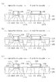
以下に、本発明の第1の実施形態に係る半導体装置の製造方法について、p型MISFETの製造方法を具体例に挙げて、図1(a) 〜(d) 、図2(a) 〜(c) 、及び図3(a) 〜(c) を参照しながら説明する。図1(a) 〜(d) 、図2(a) 〜(c) 、及び図3(a) 〜(c) は、本発明の第1の実施形態に係る半導体装置の製造方法について示す要部工程断面図であり、具体的には、内部回路用トランジスタ及び周辺回路用トランジスタを備える半導体装置の製造方法について示す要部工程断面図である。尚、図中において、左側に内部回路用MIS形成領域を示し、右側に周辺回路用MIS形成領域を示している。
(First embodiment)
In the following, with respect to the method for manufacturing a semiconductor device according to the first embodiment of the present invention, a method for manufacturing a p-type MISFET is taken as a specific example, and FIGS. 1 (a) to 1 (d) and FIGS. This will be described with reference to c) and FIGS. 3 (a) to 3 (c). 1 (a) to (d), FIGS. 2 (a) to (c), and FIGS. 3 (a) to 3 (c) show the manufacturing method of the semiconductor device according to the first embodiment of the present invention. FIG. 5 is a partial process cross-sectional view, specifically a cross-sectional view of a main part illustrating a method for manufacturing a semiconductor device including an internal circuit transistor and a peripheral circuit transistor. In the drawing, an internal circuit MIS formation region is shown on the left side, and a peripheral circuit MIS formation region is shown on the right side.
図1(a) に示すように、反応性イオンエッチングにより、シリコンよりなる半導体基板100に溝を形成し、続いて、溝内に、例えば、P−TEOS膜を埋め込むことにより、シャロートレンチ分離(STI)構造を有する素子分離領域101を形成する。
As shown in FIG. 1 (a), a trench is formed in a
続いて、熱酸化法により、半導体基板100の表面に、膜厚が5nm〜8nmのゲート絶縁膜形成膜を形成した後、フォトリソグラフィー及びエッチングにより、半導体基板100の表面における内部回路用MIS形成領域に形成されたゲート絶縁膜形成膜を選択的に除去することにより、半導体基板100の表面における周辺回路用MIS形成領域に、膜厚が5nm〜8nmの周辺回路用ゲート絶縁膜形成膜102を形成する。続いて、熱酸化法により、半導体基板100の表面における内部回路用MIS形成領域に、膜厚が2nmの内部回路用ゲート絶縁膜形成膜103を形成する。
Subsequently, after forming a gate insulating film formation film having a film thickness of 5 nm to 8 nm on the surface of the
続いて、化学気相成長法(CVD法)により、半導体基板100上に、多結晶シリコン膜104を堆積する。
Subsequently, a
次に、図1(b) に示すように、CVD法により、多結晶シリコン膜104上に、フッ素を含有する絶縁膜として、例えば、FSG(Fluorinated Silicate Glass)膜105を堆積する。ここで、FSG膜105等のフッ素を含有する絶縁膜とは、充分な量のフッ素が予め含有されてなる絶縁膜を示す。
Next, as shown in FIG. 1B, for example, an FSG (Fluorinated Silicate Glass)
次に、図1(c) に示すように、熱処理により、半導体基板100とゲート絶縁膜形成膜102、103との界面に、FSG膜105に含有されるフッ素を拡散させて導入する。これにより、半導体基板100と内部回路用ゲート絶縁膜形成膜103との界面に、内部回路用フッ素導入領域106を形成すると共に、半導体基板100と周辺回路用ゲート絶縁膜形成膜102との界面に、周辺回路用フッ素導入領域107を形成する。ここで、熱処理の条件は、FSG膜105に含有されるフッ素が、半導体基板100とゲート絶縁膜形成膜102、103との界面にまで拡散されて到達するような条件に調整される。尚、多結晶シリコン膜104は、熱処理後にはFSG膜105からのフッ素が導入されてフッ素を含有する膜となる。
Next, as shown in FIG. 1C, fluorine contained in the
次に、図1(d) に示すように、ウェットエッチングにより、FSG膜105のみを選択的に除去する。
Next, as shown in FIG. 1D, only the
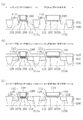
次に、図2(a) に示すように、フォトリソグラフィーにより、多結晶シリコン膜104上に、所望のゲートパターン形状を有するマスク(図示せず)を形成した後、異方性ドライエッチングにより、多結晶シリコン膜104及びゲート絶縁膜形成膜102、103におけるマスクの開口部に露出する部分を選択的に除去する。これにより、内部回路用MIS形成領域の半導体基板100上に、内部回路用ゲート絶縁膜103Aを介して、内部回路用ゲート電極108を形成すると共に、周辺回路用MIS形成領域の半導体基板100上に、周辺回路用ゲート絶縁膜102Aを介して、周辺回路用ゲート電極109を形成する。ここで、周辺回路用ゲート絶縁膜102Aは内部回路用ゲート絶縁膜103Aに比べて膜厚が厚く、又は周辺回路用ゲート電極109は内部回路用ゲート電極108に比べてゲート長が長く形成される。
Next, as shown in FIG. 2A, after a mask (not shown) having a desired gate pattern shape is formed on the
次に、図2(b) に示すように、フォトリソグラフィーにより、半導体基板100上に、内部回路用MIS形成領域を覆い、周辺回路用MIS形成領域に開口を有するレジスト膜110を形成する。続いて、周辺回路用ゲート電極109及びレジスト膜110をマスクにして、周辺回路用MIS形成領域の半導体基板100における周辺回路用ゲート電極109の両側方下に位置する領域に、例えば、BF2 等のp型不純物をイオン注入することにより、p型LDD(Lightly Doped Drain)領域111を形成した後、レジスト膜110を除去する。
Next, as shown in FIG. 2B, a resist
次に、図2(c) に示すように、CVD法により、半導体基板100上の全面に、シリコン酸化膜を堆積した後、異方性エッチングを用いてシリコン酸化膜のエッチングを行うことにより、ゲート電極108、109の側面上に、シリコン酸化膜よりなるオフセットサイドウォール112を形成する。
Next, as shown in FIG. 2C, a silicon oxide film is deposited on the entire surface of the
続いて、フォトリソグラフィーにより、半導体基板100上に、周辺回路用MIS形成領域を覆い、内部回路用MIS形成領域に開口を有するレジスト膜113を形成する。続いて、内部回路用ゲート電極108、オフセットサイドウォール112及びレジスト膜113をマスクにして、内部回路用MIS形成領域の半導体基板100における内部回路用ゲート電極108の両側方下に位置する領域に、例えば、ボロン(B)等のp型不純物をイオン注入することにより、p型エクステンション領域114を形成し、続いて、例えば、リン(P)等のn型不純物を注入することにより、n型ポケット領域115を形成した後、レジスト膜113を除去する。
Subsequently, a resist
次に、図3(a) に示すように、CVD法により、半導体基板100上の全面に、シリコン窒化膜を堆積した後、異方性エッチングを用いてシリコン窒化膜のエッチングを行うことにより、オフセットサイドウォール112の側面上に、サイドウォール116を形成する。続いて、ゲート電極108、109及びサイドウォール116をマスクに用いて、半導体基板100にボロン等のp型不純物をイオン注入することにより、内部回路用MIS形成領域の半導体基板100におけるサイドウォール116の側方下に位置する領域に、p型エクステンション領域114の接合部よりも深い接合部を有するp型ソース・ドレイン領域117aを形成すると共に、周辺回路用MIS形成領域の半導体基板100におけるサイドウォール116の側方下に位置する領域に、p型LDD領域111の接合部よりも深い接合部を有するp型ソース・ドレイン領域117bを形成する。
Next, as shown in FIG. 3A, after a silicon nitride film is deposited on the entire surface of the
次に、図3(b) に示すように、スパッタ法により、半導体基板100上の全面に、サイドウォール116、オフセットサイドウォール112、及びゲート電極108、109を覆うように、Co膜又はNi膜よりなる金属膜118を堆積する。
Next, as shown in FIG. 3B, a Co film or a Ni film is formed by sputtering so as to cover the
次に、図3(c) に示すように、アニール処理により、ゲート電極108、109及びp型ソース・ドレイン領域117a、117bに含まれるSiと、金属膜118に含まれるCo又はNiとを反応させた後、エッチングにより、素子分離領域101、サイドウォール116、及びオフセットサイドウォール112等の上に残存する未反応の金属膜118を選択的に除去する。これにより、ゲート電極108、109及びp型ソース・ドレイン領域117a、117bの表面をシリサイド化させてなるシリサイド膜119を形成する。
Next, as shown in FIG. 3C, Si contained in the
次に、通常のMISFETの製造方法と同様に、例えば、CVD法により、半導体基板100上の全面に、シリコン窒化膜及びシリコン酸化膜よりなる層間絶縁膜(図示せず)を形成した後、CMP法により、表面の平坦化を行う。続いて、層間絶縁膜に、p型ソース・ドレイン領域117a、117b及びゲート電極108、109の表面上に形成されているシリサイド膜119に到達するコンタクトホール(図示せず)を形成する。その後、各コンタクトホールの底部及び側壁に、TiN膜及びTi膜よりなるバリアメタル膜(図示せず)を形成し、続いて、各コンタクトホール内にタングステン(W)膜を埋め込む。これにより、コンタクトホール内に、バリアメタル膜を介してW膜が埋め込まれてなるコンタクトプラグ(図示せず)を形成する。その後、層間絶縁膜上に、コンタクトプラグと接続する金属配線(図示せず)を形成する。
Next, in the same way as in a normal MISFET manufacturing method, an interlayer insulating film (not shown) made of a silicon nitride film and a silicon oxide film is formed on the entire surface of the
以上のようにして、半導体基板100と内部回路用ゲート絶縁膜103Aとの界面に形成された内部回路用フッ素導入領域106を有する内部回路用トランジスタ、及び半導体基板100と周辺回路用ゲート絶縁膜102Aとの界面に形成された周辺回路用フッ素導入領域107を有する周辺回路用トランジスタを備える半導体装置を製造することができる。
As described above, the internal circuit transistor having the internal circuit
本実施形態に係る半導体装置の製造方法によると、多結晶シリコン膜104の表面を被覆するFSG膜105には、予めフッ素が充分に含有されており、しかも、従来のフッ素を含有するポリシリコン膜表面からのフッ素の外方拡散に比べて、FSG膜105表面からのフッ素の外方拡散の方が少ない。このため、FSG膜105が、フッ素の拡散源としての機能を果たすだけでなく、更には、キャップ層としての機能を果たすことができるので、フッ素の外方拡散を抑制することができる。
According to the method for manufacturing a semiconductor device according to the present embodiment, the
これにより、熱処理の際に、FSG膜105に含有されるフッ素を外方拡散させることなく、半導体基板100とゲート絶縁膜形成膜102、103との界面に拡散させて導入することができる。これにより、図1(c) に示すように、半導体基板100とゲート絶縁膜形成膜102、103との界面に、フッ素導入領域106、107を形成することができるので、半導体基板100とゲート絶縁膜形成膜102、103との界面にダングリングボンドが残存することを防止することができる。
Thereby, in the heat treatment, fluorine contained in the
したがって、内部回路用トランジスタにおいて、半導体基板100と内部回路用ゲート絶縁膜103Aとの界面に存在するダングリングボンドに起因して、NBTIの劣化が発生することを防止すると共に、周辺回路用トランジスタにおいて、半導体基板100と周辺回路用ゲート絶縁膜102Aとの界面に存在するダングリングボンドに起因して、NBTIの劣化が発生することを防止することができるので、各々が高い信頼性を有するトランジスタを備える半導体装置を提供することができる。
Therefore, in the internal circuit transistor, it is possible to prevent NBTI from being deteriorated due to the dangling bonds existing at the interface between the
このように、第1の実施形態では、FSG膜105は、キャップ層として機能するだけでなく、フッ素の拡散源としても機能する。
Thus, in the first embodiment, the
(第2の実施形態)
以下に、本発明の第2の実施形態に係る半導体装置の製造方法について、p型MISFETの製造方法を具体例に挙げて、図4(a) 〜(d) 、図5(a) 〜(c) 、及び図6(a) 〜(c) を参照しながら説明する。図4(a) 〜(d) 、図5(a) 〜(c) 、及び図6(a) 〜(c) は、本発明の第2の実施形態に係る半導体装置の製造方法について示す要部工程断面図であり、具体的には、内部回路用トランジスタ及び周辺回路用トランジスタを備える半導体装置の製造方法について示す要部工程断面図である。尚、図中において、左側に内部回路用MIS形成領域を示し、右側に周辺回路用MIS形成領域を示している。図4(a) 〜(d) 、図5(a) 〜(c) 、及び図6(a) 〜(c) において、前述した本発明の第1の実施形態に係る半導体装置と同一の構成要素については、同一の符号を付す。したがって、本実施形態では、前述した第1の実施形態と同様の説明は繰り返し行わない。
(Second Embodiment)
In the following, with respect to the method for manufacturing a semiconductor device according to the second embodiment of the present invention, a method for manufacturing a p-type MISFET is taken as a specific example, and FIGS. This will be described with reference to c) and FIGS. 6 (a) to (c). 4 (a) to (d), FIGS. 5 (a) to (c), and FIGS. 6 (a) to (c) are diagrams showing a method for manufacturing a semiconductor device according to the second embodiment of the present invention. FIG. 5 is a partial process cross-sectional view, specifically a cross-sectional view of a main part illustrating a method for manufacturing a semiconductor device including an internal circuit transistor and a peripheral circuit transistor. In the drawing, an internal circuit MIS formation region is shown on the left side, and a peripheral circuit MIS formation region is shown on the right side. 4 (a)-(d), FIGS. 5 (a)-(c), and FIGS. 6 (a)-(c), the same configuration as the semiconductor device according to the first embodiment of the present invention described above. Elements are given the same reference numerals. Therefore, in this embodiment, the same description as that of the first embodiment described above is not repeated.
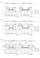
図4(a) に示すように、シリコンよりなる半導体基板100に、例えば、溝内にP−TEOS膜が埋め込まれてなる素子分離領域101を形成する。続いて、熱酸化法により、半導体基板100の表面における周辺回路用MIS形成領域に、膜厚が5nm〜8nmの周辺回路用ゲート絶縁膜形成膜102を形成した後、半導体基板100の表面における内部回路用MIS形成領域に、膜厚が2nmの内部回路用ゲート絶縁膜形成膜103を形成する。続いて、CVD法により、半導体基板100上に、多結晶シリコン膜104を堆積する。
As shown in FIG. 4A, an
次に、図4(b) に示すように、イオン注入により、多結晶シリコン膜104の全面にフッ素を注入することにより、フッ素含有多結晶シリコン膜204を形成する。ここで、フッ素含有多結晶シリコン膜204とは、第1の実施形態における多結晶シリコン膜104が熱処理前にフッ素を含有していないのに対し、熱処理前に多結晶シリコン膜中にフッ素を含有しているという意味合いを有するものである。
Next, as shown in FIG. 4B, a fluorine-containing
その後、CVD法により、フッ素含有多結晶シリコン膜204上に、フッ素を含有する絶縁膜として、例えば、FSG膜105を堆積する。
Thereafter, for example, an
次に、図4(c) に示すように、熱処理により、半導体基板100とゲート絶縁膜形成膜102、103との界面に、FSG膜105に含有されるフッ素、及びフッ素含有多結晶シリコン膜204に含まれるフッ素を拡散させて導入する。これにより、半導体基板100と内部回路用ゲート絶縁膜形成膜103との界面に、内部回路用フッ素導入領域206を形成すると共に、半導体基板100と周辺回路用ゲート絶縁膜形成膜102との界面に、周辺回路用フッ素導入領域207を形成する。ここで、熱処理の条件は、FSG膜105に含有されるフッ素、及びフッ素含有多結晶シリコン膜204に含まれるフッ素が、半導体基板100とゲート絶縁膜形成膜102、103との界面にまで拡散されて到達するような条件に調整されている。尚、フッ素含有多結晶シリコン膜204は、熱処理後には、イオン注入によって導入されたフッ素、及び熱処理によってFSG膜105から導入されたフッ素を含有する膜となる。
Next, as shown in FIG. 4C, the fluorine contained in the
次に、図4(d) に示すように、ウェットエッチングにより、FSG膜105のみを選択的に除去する。
Next, as shown in FIG. 4D, only the
次に、図5(a) に示すように、フォトリソグラフィー及び異方性ドライエッチングにより、内部回路用MIS形成領域の半導体基板100上に、内部回路用ゲート絶縁膜103Aを介して、内部回路用ゲート電極108を形成すると共に、周辺回路用MIS形成領域の半導体基板100上に、周辺回路用ゲート絶縁膜102Aを介して、周辺回路用ゲート電極109を形成する。ここで、周辺回路用ゲート絶縁膜102Aは内部回路用ゲート絶縁膜103Aに比べて膜厚が厚く、又は周辺回路用ゲート電極109は内部回路用ゲート電極108に比べてゲート長が長く形成される。
Next, as shown in FIG. 5A, the internal circuit-use
次に、図5(b) に示すように、フォトリソグラフィーにより、半導体基板100上に、内部回路用MIS形成領域を覆い、周辺回路用MIS形成領域に開口を有するレジスト膜110を形成する。続いて、周辺回路用ゲート電極109及びレジスト膜110をマスクにして、周辺回路用MIS形成領域の半導体基板100における周辺回路用ゲート電極109の両側方下に位置する領域に、例えば、BF2 等のp型不純物をイオン注入することにより、p型LDD領域111を形成した後、レジスト膜110を除去する。
Next, as shown in FIG. 5B, a resist
次に、図5(c) に示すように、CVD法により、半導体基板100上の全面に、シリコン酸化膜を堆積した後、異方性エッチングを用いてシリコン酸化膜のエッチングを行うことにより、ゲート電極108、109の側面上に、シリコン酸化膜よりなるオフセットサイドウォール112を形成する。
Next, as shown in FIG. 5C, a silicon oxide film is deposited on the entire surface of the
続いて、フォトリソグラフィーにより、半導体基板100上に、周辺回路用MIS形成領域を覆い、内部回路用MIS形成領域に開口を有するレジスト膜113を形成する。続いて、内部回路用ゲート電極108、オフセットサイドウォール112及びレジスト膜113をマスクにして、内部回路用MIS形成領域の半導体基板100における内部回路用ゲート電極108の両側方下に位置する領域に、例えば、ボロン(B)等のp型不純物をイオン注入することにより、p型エクステンション領域114を形成し、続いて、例えば、リン(P)等のn型不純物を注入することにより、n型ポケット領域115を形成した後、レジスト膜113を除去する。
Subsequently, a resist
次に、図6(a) に示すように、CVD法により、半導体基板100上の全面に、シリコン窒化膜を堆積した後、シリコン窒化膜のエッチバックにより、オフセットサイドウォール112の側面上に、サイドウォール116を形成する。続いて、半導体基板100におけるサイドウォール116の側方下に位置する領域に、例えば、B等のp型不純物をイオン注入することにより、p型ソース・ドレイン領域117a、117bを形成する。
Next, as shown in FIG. 6A, after a silicon nitride film is deposited on the entire surface of the
次に、図6(b) に示すように、スパッタ法により、半導体基板100上の全面に、サイドウォール116、オフセットサイドウォール112、及びゲート電極108、109を覆うように、Co膜又はNi膜よりなる金属膜118を堆積する。
Next, as shown in FIG. 6B, a Co film or Ni film is formed by sputtering so as to cover the
次に、図6(c) に示すように、アニール処理により、ゲート電極108、109及びp型ソース・ドレイン領域117a、117bに含まれるSiと、金属膜118に含まれるCo又はNiとを反応させた後、エッチングにより、半導体基板100上に残存する未反応の金属膜118を選択的に除去する。これにより、ゲート電極108、109及びp型ソース・ドレイン領域117a、117bの表面をシリサイド化させてなるシリサイド膜119を形成する。
Next, as shown in FIG. 6C, Si contained in the
次に、通常のMISFETの製造方法と同様に、例えば、CVD法により、半導体基板100上の全面に、シリコン窒化膜及びシリコン酸化膜よりなる層間絶縁膜(図示せず)を形成した後、CMP法により、表面の平坦化を行う。続いて、層間絶縁膜に、p型ソース・ドレイン領域117a、117b及びゲート電極108、109の表面上に形成されているシリサイド膜119に到達するコンタクトホール(図示せず)を形成する。その後、各コンタクトホールの底部及び側壁に、TiN膜及びTi膜よりなるバリアメタル膜(図示せず)を形成し、続いて、各コンタクトホール内にタングステン(W)膜を埋め込む。これにより、コンタクトホール内に、バリアメタル膜を介してW膜が埋め込まれてなるコンタクトプラグ(図示せず)を形成する。その後、層間絶縁膜上に、コンタクトプラグと接続する金属配線(図示せず)を形成する。
Next, in the same way as in a normal MISFET manufacturing method, an interlayer insulating film (not shown) made of a silicon nitride film and a silicon oxide film is formed on the entire surface of the
以上のようにして、半導体基板100と内部回路用ゲート絶縁膜103Aとの界面に形成された内部回路用フッ素導入領域206を有する内部回路用トランジスタ、及び半導体基板100と周辺回路用ゲート絶縁膜102Aとの界面に形成された周辺回路用フッ素導入領域207を有する周辺回路用トランジスタを備える半導体装置を製造することができる。
As described above, the internal circuit transistor having the internal circuit
本実施形態に係る半導体装置の製造方法によると、フッ素含有多結晶シリコン膜204の表面を被覆するFSG膜105には、予めフッ素が充分に含有されているため、熱処理の際に、FSG膜105中にフッ素含有多結晶シリコン膜204からのフッ素が侵入する経路がなく、FSG膜105はキャップ層としての機能を果たすことができるので、フッ素の外方拡散が起こることを確実に防止することができる。
According to the method for manufacturing a semiconductor device according to the present embodiment, the
これにより、熱処理の際に、FSG膜105に含有されるフッ素を外方拡散させることなく、半導体基板100とゲート絶縁膜形成膜102、103との界面に拡散させて導入するだけでなく、更には、フッ素含有多結晶シリコン膜204に注入されたフッ素をも外方拡散させることなく、半導体基板100とゲート絶縁膜形成膜102、103との界面に拡散させて導入することができるので、前述した第1の実施形態と比較して、フッ素導入領域206、207に導入されるフッ素濃度の高濃度化を図ることができる。
Thus, in the heat treatment, fluorine contained in the
このため、半導体基板100とゲート絶縁膜形成膜102、103との界面に、充分な量のフッ素(すなわち、ダングリングボンド量に相当する量のフッ素)を確実に拡散させて導入することができるので、半導体基板100とゲート絶縁膜形成膜102、103との界面にダングリングボンドが残存することを確実に防止することができる。
For this reason, a sufficient amount of fluorine (that is, an amount of fluorine corresponding to the amount of dangling bonds) can be reliably diffused and introduced into the interface between the
したがって、内部回路用トランジスタにおいて、半導体基板100と内部回路用ゲート絶縁膜103Aとの界面に存在するダングリングボンドに起因して、NBTIの劣化が発生することを防止すると共に、周辺回路用トランジスタにおいて、半導体基板100と周辺回路用ゲート絶縁膜102Aとの界面に存在するダングリングボンドに起因して、NBTIの劣化が発生することを防止することができるので、各々が高い信頼性を有するトランジスタを備える半導体装置を提供することができる。
Therefore, in the internal circuit transistor, it is possible to prevent NBTI from being deteriorated due to the dangling bonds existing at the interface between the
このように、本実施形態では、FSG膜105は、前述した第1の実施形態と同様に、フッ素の拡散源としての機能も果たすが、主に、キャップ層としての機能を果たしており、具体的には、熱処理の際に、フッ素含有多結晶シリコン膜204に含まれるフッ素が外方拡散されることを確実に防止する機能を果たす。これに対し、前述した第1の実施形態では、FSG膜105は、キャップ層としての機能及びフッ素の拡散源としての機能の双方を果たす。
As described above, in the present embodiment, the
(第3の実施形態)
以下に、本発明の第3の実施形態に係る半導体装置の製造方法について、p型MISFETの製造方法を具体例に挙げて、図7(a) 〜(d) 、図8(a) 〜(c) 、及び図9(a) 〜(c) を参照しながら説明する。図7(a) 〜(d) 、図8(a) 〜(c) 、及び図9(a) 〜(c) は、本発明の第3の実施形態に係る半導体装置の製造方法について示す要部工程断面図であり、具体的には、内部回路用トランジスタ及び周辺回路用トランジスタを備える半導体装置の製造方法について示す要部工程断面図である。尚、図中において、左側に内部回路用MIS形成領域を示し、右側に周辺回路用MIS形成領域を示している。図7(a) 〜(d) 、図8(a) 〜(c) 、及び図9(a) 〜(c) において、前述した本発明の第1の実施形態に係る半導体装置と同一の構成要素については、同一の符号を付す。したがって、本実施形態では、前述した第1の実施形態と同様の説明は繰り返し行わない。
(Third embodiment)
In the following, with respect to the method for manufacturing a semiconductor device according to the third embodiment of the present invention, a method for manufacturing a p-type MISFET is taken as a specific example, and FIGS. This will be described with reference to c) and FIGS. 9 (a) to 9 (c). 7 (a) to (d), FIGS. 8 (a) to (c), and FIGS. 9 (a) to 9 (c) are diagrams showing the manufacturing method of the semiconductor device according to the third embodiment of the present invention. FIG. 5 is a partial process cross-sectional view, specifically a cross-sectional view of a main part illustrating a method for manufacturing a semiconductor device including an internal circuit transistor and a peripheral circuit transistor. In the drawing, an internal circuit MIS formation region is shown on the left side, and a peripheral circuit MIS formation region is shown on the right side. 7 (a)-(d), FIGS. 8 (a)-(c), and FIGS. 9 (a)-(c), the same configuration as the semiconductor device according to the first embodiment of the present invention described above. Elements are given the same reference numerals. Therefore, in this embodiment, the same description as that of the first embodiment described above is not repeated.
図7(a) に示すように、シリコンよりなる半導体基板100に、例えば、溝内にP−TEOS膜が埋め込まれてなる素子分離領域101を形成する。続いて、熱酸化法により、半導体基板100の表面における周辺回路用MIS形成領域に、膜厚が5nm〜8nmの周辺回路用ゲート絶縁膜形成膜102を形成した後、半導体基板100の表面における内部回路用MIS形成領域に、膜厚が2nmの内部回路用ゲート絶縁膜形成膜103を形成する。続いて、CVD法により、半導体基板100上に、多結晶シリコン膜104を堆積する。その後、多結晶シリコン膜104上に、内部回路用MIS形成領域を覆い、周辺回路用MIS形成領域に開口を有するレジスト膜304Rを形成する。その後、多結晶シリコン膜104におけるレジスト膜304Rの開口部に露出する部分(すなわち、多結晶シリコン膜104における周辺回路用MIS形成領域)に、フッ素を選択的にイオン注入することにより、フッ素含有多結晶シリコン膜304を選択的に形成する。
As shown in FIG. 7A, for example, an
次に、図7(b) に示すように、レジスト膜304Rを除去した後、CVD法により、多結晶シリコン膜104及びフッ素含有多結晶シリコン膜304上に、フッ素を含有する絶縁膜として、例えば、FSG膜105を堆積する。
Next, as shown in FIG. 7B, after removing the resist
次に、図7(c) に示すように、熱処理により、半導体基板100とゲート絶縁膜形成膜102、103との界面に、FSG膜105に含まれるフッ素を拡散させて導入すると共に、半導体基板100と周辺回路用ゲート絶縁膜形成膜102との界面のみに、フッ素含有多結晶シリコン膜304に注入されたフッ素を選択的に拡散させて導入する。これにより、半導体基板100と内部回路用ゲート絶縁膜形成膜103との界面に、内部回路用フッ素導入領域306を形成すると共に、半導体基板100と周辺回路用ゲート絶縁膜形成膜102との界面に、周辺回路用フッ素導入領域307を形成する。
Next, as shown in FIG. 7C, the fluorine contained in the
次に、図7(d) に示すように、ウェットエッチングにより、FSG膜105のみを選択的に除去する。
Next, as shown in FIG. 7D, only the
次に、図8(a) に示すように、フォトリソグラフィー及び異方性ドライエッチングにより、内部回路用MIS形成領域の半導体基板100上に、内部回路用ゲート絶縁膜103Aを介して、内部回路用ゲート電極108を形成すると共に、周辺回路用MIS形成領域の半導体基板100上に、周辺回路用ゲート絶縁膜102Aを介して、周辺回路用ゲート電極109を形成する。ここで、周辺回路用ゲート絶縁膜102Aは内部回路用ゲート絶縁膜103Aに比べて膜厚が厚く、又は周辺回路用ゲート電極109は内部回路用ゲート電極108に比べてゲート長が長く形成される。
Next, as shown in FIG. 8A, the internal circuit-use
次に、図8(b) に示すように、フォトリソグラフィーにより、半導体基板100上に、内部回路用MIS形成領域を覆い、周辺回路用MIS形成領域に開口を有するレジスト膜110を形成する。続いて、周辺回路用ゲート電極109及びレジスト膜110をマスクにして、周辺回路用MIS形成領域の半導体基板100における周辺回路用ゲート電極109の両側方下に位置する領域に、例えば、BF2 等のp型不純物をイオン注入することにより、p型LDD領域111を形成した後、レジスト膜110を除去する。
Next, as shown in FIG. 8B, a resist
次に、図8(c) に示すように、CVD法により、半導体基板100上の全面に、シリコン酸化膜を堆積した後、異方性エッチングを用いてシリコン酸化膜のエッチングを行うことにより、ゲート電極108、109の側面上に、シリコン酸化膜よりなるオフセットサイドウォール112を形成する。
Next, as shown in FIG. 8C, a silicon oxide film is deposited on the entire surface of the
続いて、フォトリソグラフィーにより、半導体基板100上に、周辺回路用MIS形成領域を覆い、内部回路用MIS形成領域に開口を有するレジスト膜113を形成する。続いて、内部回路用ゲート電極108、オフセットサイドウォール112及びレジスト膜113をマスクにして、内部回路用MIS形成領域の半導体基板100における内部回路用ゲート電極108の両側方下に位置する領域に、例えば、ボロン(B)等のp型不純物をイオン注入することにより、p型エクステンション領域114を形成し、続いて、例えば、リン(P)等のn型不純物を注入することにより、n型ポケット領域115を形成した後、レジスト膜113を除去する。
Subsequently, a resist
次に、図9(a) に示すように、CVD法により、半導体基板100上の全面に、シリコン窒化膜を堆積した後、シリコン窒化膜のエッチバックにより、オフセットサイドウォール112の側面上に、サイドウォール116を形成する。続いて、半導体基板100におけるサイドウォール116の側方下に位置する領域に、例えば、B等のp型不純物をイオン注入することにより、p型ソース・ドレイン領域117a、117bを形成する。
Next, as shown in FIG. 9A, after a silicon nitride film is deposited on the entire surface of the
次に、図9(b) に示すように、スパッタ法により、半導体基板100上の全面に、サイドウォール116、オフセットサイドウォール112、及びゲート電極108、109を覆うように、Co膜又はNi膜よりなる金属膜118を堆積する。
Next, as shown in FIG. 9B, a Co film or a Ni film is formed by sputtering so as to cover the
次に、図9(c) に示すように、アニール処理により、ゲート電極108、109及びp型ソース・ドレイン領域117a、117bに含まれるSiと、金属膜118に含まれるCo又はNiとを反応させた後、エッチングにより、半導体基板100上に残存する未反応の金属膜118を選択的に除去する。これにより、ゲート電極108、109及びp型ソース・ドレイン領域117a、117bの表面をシリサイド化させてなるシリサイド膜119を形成する。
Next, as shown in FIG. 9C, Si contained in the
次に、通常のMISFETの製造方法と同様に、例えば、CVD法により、半導体基板100上の全面に、シリコン窒化膜及びシリコン酸化膜よりなる層間絶縁膜(図示せず)を形成した後、CMP法により、表面の平坦化を行う。続いて、層間絶縁膜に、p型ソース・ドレイン領域117a、117b及びゲート電極108、109の表面上に形成されているシリサイド膜119に到達するコンタクトホール(図示せず)を形成する。その後、各コンタクトホールの底部及び側壁に、TiN膜及びTi膜よりなるバリアメタル膜(図示せず)を形成し、続いて、各コンタクトホール内にタングステン(W)膜を埋め込む。これにより、コンタクトホール内に、バリアメタル膜を介してW膜が埋め込まれてなるコンタクトプラグ(図示せず)を形成する。その後、層間絶縁膜上に、コンタクトプラグと接続する金属配線(図示せず)を形成する。
Next, in the same way as in a normal MISFET manufacturing method, an interlayer insulating film (not shown) made of a silicon nitride film and a silicon oxide film is formed on the entire surface of the
以上のようにして、半導体基板100と内部回路用ゲート絶縁膜103Aとの界面に形成された内部回路用フッ素導入領域306を有する内部回路用トランジスタ、及び半導体基板100と周辺回路用ゲート絶縁膜102Aとの界面に形成された周辺回路用フッ素導入領域307を有する周辺回路用トランジスタを備える半導体装置を製造することができる。
As described above, the internal circuit transistor having the internal circuit
本実施形態に係る半導体装置の製造方法によると、図7(c) に示すように、多結晶シリコン膜104及びフッ素含有多結晶シリコン膜304の表面を被覆するFSG膜105には、予めフッ素が充分に含有されているため、熱処理の際に、FSG膜105中にフッ素含有多結晶シリコン膜304からのフッ素が侵入する経路がなく、FSG膜105はキャップ層としての機能を果たすことができるので、フッ素の外方拡散が起こることを確実に防止することができる。
According to the method for manufacturing a semiconductor device according to the present embodiment, as shown in FIG. 7C, the
これにより、熱処理の際に、FSG膜105に含有されるフッ素を外方拡散させることなく、半導体基板100とゲート絶縁膜形成膜102、103との界面に拡散させて導入すると共に、フッ素含有多結晶シリコン膜304に注入されたフッ素を外方拡散させることなく、半導体基板100と周辺回路用ゲート絶縁膜形成膜102との界面のみに選択的に拡散させて導入することができるので、半導体基板100と内部回路用ゲート絶縁膜形成膜103との界面に、内部回路用フッ素導入領域306を得ると共に、半導体基板100と周辺回路用ゲート絶縁膜形成膜102との界面に、内部回路用フッ素導入領域306に導入されるフッ素濃度よりも高いフッ素濃度を有する周辺回路用フッ素導入領域307を得ることができる。
Thus, in the heat treatment, fluorine contained in the
本実施形態に係る半導体装置の製造方法では、図7(a) に示すように、多結晶シリコン膜104上における内部回路用MIS形成領域を覆うレジスト膜304Rを用いて、多結晶シリコン膜104における周辺回路用MIS形成領域に、フッ素を選択的に注入することにより、フッ素含有多結晶シリコン膜304を選択的に形成する。
In the method of manufacturing a semiconductor device according to the present embodiment, as shown in FIG. 7A, a resist
これにより、熱処理の際に、NBTI劣化量が大きいと予想される周辺回路用トランジスタを構成する周辺回路用ゲート絶縁膜形成膜102と半導体基板100との界面のみに、FSG膜105に含有されるフッ素を拡散させて導入するだけでなく、フッ素含有多結晶シリコン膜304に注入されたフッ素を拡散させて導入する一方、NBTI劣化量が小さいと予想される内部回路用トランジスタを構成する内部回路用ゲート絶縁膜形成膜103と半導体基板100との界面に、FSG膜105に含有されるフッ素のみを拡散させて導入することができる。
Thus, during the heat treatment, the
このように、各トランジスタにおけるNBTIの劣化量に基づいて、多結晶シリコン膜104にフッ素を選択的に注入することによって、熱処理の際に、NBTIの劣化が特に発生すると予想される周辺回路用トランジスタを構成する周辺回路用ゲート絶縁膜形成膜102と半導体基板100との界面のみに、フッ素含有多結晶シリコン膜304に注入されたフッ素を選択的に拡散させて導入することができるので、周辺回路用トランジスタにおいて、NBTIの劣化が発生することを効果的に防止することができる。
Thus, by selectively injecting fluorine into the
更には、内部回路用トランジスタを構成する半導体基板100と内部回路用ゲート絶縁膜形成膜103との界面に、FSG膜105に含有されるフッ素のみを選択的に拡散させて導入することができるので、不必要な量のフッ素(すなわち、ダングリングボンド量以上のフッ素)が導入されることを効果的に防止すると共に、内部回路用トランジスタにおいて、NBTIの劣化が発生することを防止することができる。
Furthermore, only fluorine contained in the
尚、本発明の各実施形態では、半導体装置の製造方法としてp型MISFETの製造方法を具体例に挙げて説明したが、本発明はこれに限定されることはなく、n型MISFETの製造方法においても本発明の各実施形態と同様に製造することができる。 In each of the embodiments of the present invention, the manufacturing method of the p-type MISFET is described as a specific example of the manufacturing method of the semiconductor device. However, the present invention is not limited to this, and the manufacturing method of the n-type MISFET Can be produced in the same manner as in the embodiments of the present invention.
また、本発明の各実施形態では、内部回路用トランジスタ及び周辺回路用トランジスタの双方を有する半導体装置について説明したが、本発明はこれに限定されることはなく、例えば、内部回路用トランジスタのみを有する半導体装置、又は周辺回路用トランジスタのみを有する半導体装置においても、本発明と同様の効果を得ることができる。 In each embodiment of the present invention, the semiconductor device having both the internal circuit transistor and the peripheral circuit transistor has been described. However, the present invention is not limited to this, and for example, only the internal circuit transistor is provided. The same effects as those of the present invention can be obtained also in a semiconductor device having a semiconductor device having only a peripheral circuit transistor.
また、第3の実施形態では、多結晶シリコン膜104における周辺回路用MIS形成領域に、フッ素を選択的に注入する場合を具体例に挙げて説明したが、本発明はこれに限定されることはなく、多結晶シリコン膜におけるNBTI劣化量が大きいと予想されるMIS形成領域に、フッ素を選択的に注入することにより、前述した第3の実施形態と同様の効果を得ることができる。
In the third embodiment, the case of selectively injecting fluorine into the peripheral circuit MIS formation region in the
例えば、ゲート絶縁膜の更なる薄膜化が進行すると、ゲート絶縁膜の誘電率の確保を目的に、ゲート絶縁膜に導入される窒素量が増加する。ここで、ゲート絶縁膜に導入された窒素は固定電荷となるので、ゲート絶縁膜に導入される窒素量の増加に伴って、半導体基板とゲート絶縁膜との界面に存在する固定電荷量が増加しNBTIの劣化に影響する。この場合、内部回路用トランジスタにおけるNBTIの劣化が問題となることが考えられ、周辺回路用トランジスタにおけるNBTIの劣化量よりも大きくなるおそれがあるので、多結晶シリコン膜における内部回路用MIS形成領域に、フッ素を選択的に注入することにより、前述した第3の実施形態と同様の効果を得ることができる。 For example, when the gate insulating film is further thinned, the amount of nitrogen introduced into the gate insulating film increases for the purpose of securing the dielectric constant of the gate insulating film. Here, since the nitrogen introduced into the gate insulating film becomes a fixed charge, the amount of fixed charge existing at the interface between the semiconductor substrate and the gate insulating film increases as the amount of nitrogen introduced into the gate insulating film increases. It affects the degradation of NBTI. In this case, degradation of NBTI in the internal circuit transistor is considered to be a problem and may be larger than the degradation amount of NBTI in the peripheral circuit transistor. Therefore, in the internal circuit MIS formation region in the polycrystalline silicon film. By selectively injecting fluorine, the same effect as in the third embodiment described above can be obtained.
本発明は、熱処理による基板とゲート絶縁膜形成膜との界面へのフッ素の導入工程の際に、フッ素の外方拡散が起こることを確実に防止することができるため、基板とゲート絶縁膜との界面に存在するダングリングボンドに起因して、NBTIの劣化が発生することを防止することができるので、半導体装置の製造方法に有用である。 Since the present invention can reliably prevent out-diffusion of fluorine during the process of introducing fluorine into the interface between the substrate and the gate insulating film forming film by heat treatment, the substrate and the gate insulating film Since NBTI can be prevented from deteriorating due to dangling bonds existing at the interface of the semiconductor device, it is useful for a method for manufacturing a semiconductor device.
100 半導体基板
101 素子分離領域
102 周辺回路用ゲート絶縁膜形成膜
102A 周辺回路用ゲート絶縁膜
103 内部回路用ゲート絶縁膜形成膜
103A 内部回路用ゲート絶縁膜
104 多結晶シリコン膜
204、304 フッ素含有多結晶シリコン膜
304R レジスト膜
105 FSG膜
106、206、306 内部回路用フッ素導入領域
107、207、307 周辺回路用フッ素導入領域
108 内部回路用ゲート電極
109 周辺回路用ゲート電極
110 レジスト膜
111 p型LDD領域
112 オフセットサイドウォール
113 レジスト膜
114 p型エクステンション領域
115 n型ポケット領域
116 サイドウォール
117a、117b p型ソース・ドレイン領域
118 金属膜
119 シリサイド膜
DESCRIPTION OF
Claims (8)
前記ゲート絶縁膜形成膜上にゲート電極形成膜を形成する工程(b)と、
前記ゲート電極形成膜上にフッ素を含有する絶縁膜を形成する工程(c)と、
熱処理により、前記半導体基板と前記ゲート絶縁膜形成膜との界面に、前記フッ素を含有する絶縁膜に含有されるフッ素を拡散させて導入する工程(d)とを備えることを特徴とする半導体装置の製造方法。 A step (a) of forming a gate insulating film formation film in an element formation region on the semiconductor substrate;
A step (b) of forming a gate electrode formation film on the gate insulation film formation film;
A step (c) of forming an insulating film containing fluorine on the gate electrode forming film;
A step (d) of diffusing and introducing fluorine contained in the insulating film containing fluorine into the interface between the semiconductor substrate and the gate insulating film forming film by heat treatment; Manufacturing method.
前記工程(d)は、前記半導体基板と前記ゲート絶縁膜形成膜との界面に、前記ゲート電極形成膜に注入されたフッ素を拡散させて導入する工程を更に含むことを特徴とする請求項1に記載の半導体装置の製造方法。 A step (x) of injecting fluorine into the gate electrode formation film after the step (b) and before the step (c);
2. The step (d) further includes a step of diffusing and introducing fluorine implanted into the gate electrode forming film into an interface between the semiconductor substrate and the gate insulating film forming film. The manufacturing method of the semiconductor device as described in any one of Claims 1-3.
前記ゲート絶縁膜形成膜及び前記ゲート電極形成膜をパターニングすることにより、ゲート絶縁膜及びゲート電極を形成する工程(f)と、
前記工程(f)よりも後に、前記半導体基板における前記ゲート電極の側方下に位置する領域にエクステンション領域を形成する工程(g)とを更に備えることを特徴とする請求項1又は2に記載の半導体装置の製造方法。 A step (e) of removing the fluorine-containing insulating film after the step (d);
(F) forming a gate insulating film and a gate electrode by patterning the gate insulating film forming film and the gate electrode forming film;
3. The method according to claim 1, further comprising a step (g) of forming an extension region in a region located laterally below the gate electrode in the semiconductor substrate after the step (f). Semiconductor device manufacturing method.
前記工程(h)よりも後に、前記半導体基板における前記サイドウォールの側方下に位置する領域に、ソース・ドレイン領域を形成する工程(i)とを更に備えることを特徴とする請求項3に記載の半導体装置の製造方法。 A step (h) of forming a sidewall on a side surface of the gate electrode after the step (g);
4. The method according to claim 3, further comprising a step (i) of forming a source / drain region in a region located laterally below the sidewall in the semiconductor substrate after the step (h). The manufacturing method of the semiconductor device of description.
前記工程(b)は、前記第1のゲート絶縁膜形成膜上に、前記ゲート電極形成膜を構成する第1のゲート電極形成膜を形成すると共に、前記第2のゲート絶縁膜形成膜上に、前記ゲート電極形成膜を構成する第2のゲート電極形成膜を形成する工程を含むことを特徴とする請求項1に記載の半導体装置の製造方法。 In the step (a), a first gate insulating film forming film constituting the gate insulating film forming film is formed in a first region in the element forming region, and the first region in the element forming region is formed. Forming a second gate insulating film forming film constituting the gate insulating film forming film in a second region different from
In the step (b), a first gate electrode forming film constituting the gate electrode forming film is formed on the first gate insulating film forming film, and on the second gate insulating film forming film. 2. The method of manufacturing a semiconductor device according to claim 1, further comprising a step of forming a second gate electrode forming film constituting the gate electrode forming film.
前記工程(d)は、前記半導体基板と前記ゲート絶縁膜形成膜との界面に、前記ゲート電極形成膜に注入されたフッ素を拡散させて導入する工程を更に含むことを特徴とする請求項5に記載の半導体装置の製造方法。 A step of injecting fluorine into at least one of the first gate electrode formation film and the second gate electrode formation film after the step (b) and before the step (c). Further including (x),
6. The step (d) further includes a step of diffusing and introducing fluorine implanted into the gate electrode formation film into an interface between the semiconductor substrate and the gate insulating film formation film. The manufacturing method of the semiconductor device as described in any one of Claims 1-3.
前記第1のゲート絶縁膜形成膜及び前記第1のゲート電極形成膜をパターニングすることにより、第1のゲート絶縁膜及び第1のゲート電極を形成すると共に、前記第2のゲート絶縁膜形成膜及び前記第2のゲート電極形成膜をパターニングすることにより、第2のゲート絶縁膜及び第2のゲート電極を形成する工程(f)と、
前記工程(f)よりも後に、前記半導体基板における前記第1のゲート電極の側方下に位置する領域にエクステンション領域を形成すると共に、前記半導体基板における前記第2のゲート電極の側方下に位置する領域にLDD領域を形成する工程(g)とを更に備えることを特徴とする請求項5又は6に記載の半導体装置の製造方法。 A step (e) of removing the fluorine-containing insulating film after the step (d);
By patterning the first gate insulating film forming film and the first gate electrode forming film, the first gate insulating film and the first gate electrode are formed, and the second gate insulating film forming film is formed. And (f) forming a second gate insulating film and a second gate electrode by patterning the second gate electrode formation film,
After the step (f), an extension region is formed in a region of the semiconductor substrate located laterally below the first gate electrode, and is formed laterally below the second gate electrode of the semiconductor substrate. The method of manufacturing a semiconductor device according to claim 5, further comprising a step (g) of forming an LDD region in a region to be positioned.
前記工程(h)よりも後に、前記半導体基板における前記第1のサイドウォールの側方下に位置する領域に、第1のソース・ドレイン領域を形成すると共に、前記半導体基板における前記第2のサイドウォールの側方下に位置する領域に、第2のソース・ドレイン領域を形成する工程(i)とを更に備えることを特徴とする請求項7に記載の半導体装置の製造方法。 A step (h) of forming a first sidewall on the side surface of the first gate electrode and forming a second sidewall on the side surface of the second gate electrode after the step (g). )When,
After the step (h), a first source / drain region is formed in a region located laterally below the first sidewall in the semiconductor substrate, and the second side in the semiconductor substrate is formed. The method of manufacturing a semiconductor device according to claim 7, further comprising a step (i) of forming a second source / drain region in a region located below the side of the wall.
Priority Applications (2)
| Application Number | Priority Date | Filing Date | Title |
|---|---|---|---|
| JP2006015004A JP2007200976A (en) | 2006-01-24 | 2006-01-24 | Method for manufacturing semiconductor device |
| US11/540,756 US20070173023A1 (en) | 2006-01-24 | 2006-10-02 | Semiconductor device manufacturing method |
Applications Claiming Priority (1)
| Application Number | Priority Date | Filing Date | Title |
|---|---|---|---|
| JP2006015004A JP2007200976A (en) | 2006-01-24 | 2006-01-24 | Method for manufacturing semiconductor device |
Publications (1)
| Publication Number | Publication Date |
|---|---|
| JP2007200976A true JP2007200976A (en) | 2007-08-09 |
Family
ID=38286071
Family Applications (1)
| Application Number | Title | Priority Date | Filing Date |
|---|---|---|---|
| JP2006015004A Pending JP2007200976A (en) | 2006-01-24 | 2006-01-24 | Method for manufacturing semiconductor device |
Country Status (2)
| Country | Link |
|---|---|
| US (1) | US20070173023A1 (en) |
| JP (1) | JP2007200976A (en) |
Cited By (4)
| Publication number | Priority date | Publication date | Assignee | Title |
|---|---|---|---|---|
| JP2010232362A (en) * | 2009-03-26 | 2010-10-14 | Oki Semiconductor Co Ltd | Semiconductor element and method of manufacturing the same |
| WO2013132766A1 (en) * | 2012-03-08 | 2013-09-12 | 旭化成エレクトロニクス株式会社 | Method for manufacturing semiconductor device |
| US9236455B2 (en) | 2013-07-10 | 2016-01-12 | Samsung Display Co., Ltd. | Thin film transistor substrate and method of manufacturing the same |
| WO2018216309A1 (en) * | 2017-05-22 | 2018-11-29 | シャープ株式会社 | Solid-state imaging element, method for manufacturing solid-state imaging element, and electronic device |
Families Citing this family (3)
| Publication number | Priority date | Publication date | Assignee | Title |
|---|---|---|---|---|
| JP2008300779A (en) * | 2007-06-04 | 2008-12-11 | Elpida Memory Inc | Semiconductor device and manufacturing method therefor |
| KR20100073439A (en) * | 2008-12-23 | 2010-07-01 | 주식회사 동부하이텍 | Semiconductor device and method for manufacturing the same |
| JP2010245366A (en) * | 2009-04-08 | 2010-10-28 | Fujifilm Corp | Electronic device, method of manufacturing the same, and display device |
Family Cites Families (10)
| Publication number | Priority date | Publication date | Assignee | Title |
|---|---|---|---|---|
| KR970009276B1 (en) * | 1993-10-28 | 1997-06-09 | 금성일렉트론 주식회사 | Method for manufacturing moset |
| US5712208A (en) * | 1994-06-09 | 1998-01-27 | Motorola, Inc. | Methods of formation of semiconductor composite gate dielectric having multiple incorporated atomic dopants |
| US5571734A (en) * | 1994-10-03 | 1996-11-05 | Motorola, Inc. | Method for forming a fluorinated nitrogen containing dielectric |
| US5665611A (en) * | 1996-01-31 | 1997-09-09 | Micron Technology, Inc. | Method of forming a thin film transistor using fluorine passivation |
| US6825132B1 (en) * | 1996-02-29 | 2004-11-30 | Sanyo Electric Co., Ltd. | Manufacturing method of semiconductor device including an insulation film on a conductive layer |
| JP2000269492A (en) * | 1999-03-16 | 2000-09-29 | Nec Corp | Manufacture of semiconductor device |
| US6432786B2 (en) * | 2000-08-10 | 2002-08-13 | National Science Council | Method of forming a gate oxide layer with an improved ability to resist the process damage |
| US6825133B2 (en) * | 2003-01-22 | 2004-11-30 | Taiwan Semiconductor Manufacturing Company, Ltd. | Use of fluorine implantation to form a charge balanced nitrided gate dielectric layer |
| CN1790642A (en) * | 2004-11-08 | 2006-06-21 | 松下电器产业株式会社 | Method for fabricating semiconductor device |
| US20070218663A1 (en) * | 2006-03-20 | 2007-09-20 | Texas Instruments Inc. | Semiconductor device incorporating fluorine into gate dielectric |
-
2006
- 2006-01-24 JP JP2006015004A patent/JP2007200976A/en active Pending
- 2006-10-02 US US11/540,756 patent/US20070173023A1/en not_active Abandoned
Cited By (8)
| Publication number | Priority date | Publication date | Assignee | Title |
|---|---|---|---|---|
| JP2010232362A (en) * | 2009-03-26 | 2010-10-14 | Oki Semiconductor Co Ltd | Semiconductor element and method of manufacturing the same |
| WO2013132766A1 (en) * | 2012-03-08 | 2013-09-12 | 旭化成エレクトロニクス株式会社 | Method for manufacturing semiconductor device |
| US9034709B2 (en) | 2012-03-08 | 2015-05-19 | Asahi Kasei Microdevices Corporation | Method for manufacturing semiconductor device |
| JP5723483B2 (en) * | 2012-03-08 | 2015-05-27 | 旭化成エレクトロニクス株式会社 | Manufacturing method of semiconductor device |
| KR101567738B1 (en) | 2012-03-08 | 2015-11-09 | 아사히 가세이 일렉트로닉스 가부시끼가이샤 | Method for manufacturing semiconductor device |
| US9236455B2 (en) | 2013-07-10 | 2016-01-12 | Samsung Display Co., Ltd. | Thin film transistor substrate and method of manufacturing the same |
| WO2018216309A1 (en) * | 2017-05-22 | 2018-11-29 | シャープ株式会社 | Solid-state imaging element, method for manufacturing solid-state imaging element, and electronic device |
| JPWO2018216309A1 (en) * | 2017-05-22 | 2020-02-27 | シャープ株式会社 | Solid-state imaging device, method of manufacturing solid-state imaging device, and electronic device |
Also Published As
| Publication number | Publication date |
|---|---|
| US20070173023A1 (en) | 2007-07-26 |
Similar Documents
| Publication | Publication Date | Title |
|---|---|---|
| US7238996B2 (en) | Semiconductor device | |
| JP5268829B2 (en) | Semiconductor device | |
| JP2000332237A (en) | Manufacture of semiconductor device | |
| JP2007200976A (en) | Method for manufacturing semiconductor device | |
| JP2007227851A (en) | Semiconductor device, and its manufacturing method | |
| JP2003249657A (en) | Method for manufacturing semiconductor device | |
| JP2003017555A (en) | Semiconductor integrated circuit device and method of manufacturing same | |
| US6794258B2 (en) | High-performance MOS transistor of LDD structure having a gate insulating film with a nitride central portion and oxide end portions | |
| JP2006202860A (en) | Semiconductor device and its manufacturing method | |
| JP4040602B2 (en) | Semiconductor device | |
| US6744113B2 (en) | Semiconductor device with element isolation using impurity-doped insulator and oxynitride film | |
| US7550357B2 (en) | Semiconductor device and fabricating method thereof | |
| KR20070086148A (en) | Semiconductor device and method for manufacturing same | |
| JP2007288051A (en) | Semiconductor device, and manufacturing method thereof | |
| US7964917B2 (en) | Semiconductor device including liner insulating film | |
| US20050127446A1 (en) | Semiconductor device and method for manufacturing semiconductor device | |
| KR100632043B1 (en) | Method for manufacturing mos transistor | |
| JP2004186359A (en) | Semiconductor integrated circuit device and its manufacturing method | |
| JP3469738B2 (en) | Semiconductor device | |
| JP2008047820A (en) | Semiconductor device and manufacturing method thereof | |
| KR100691491B1 (en) | Dual gate of semiconductor device and method for forming the same | |
| KR100611786B1 (en) | Method for fabrication of mos transistor | |
| JP2005252052A (en) | Semiconductor device and its manufacturing method | |
| KR100236265B1 (en) | Method of manufacturing semiconductor device | |
| KR100221620B1 (en) | Semiconductor device and the manufacturing method thereof |