JP2007165358A - Chip-type capacitor - Google Patents
Chip-type capacitor Download PDFInfo
- Publication number
- JP2007165358A JP2007165358A JP2005355802A JP2005355802A JP2007165358A JP 2007165358 A JP2007165358 A JP 2007165358A JP 2005355802 A JP2005355802 A JP 2005355802A JP 2005355802 A JP2005355802 A JP 2005355802A JP 2007165358 A JP2007165358 A JP 2007165358A
- Authority
- JP
- Japan
- Prior art keywords
- electrode
- resistor
- chip
- side edge
- protrusion
- Prior art date
- Legal status (The legal status is an assumption and is not a legal conclusion. Google has not performed a legal analysis and makes no representation as to the accuracy of the status listed.)
- Pending
Links
Images


Abstract
Description
本発明は、チップ抵抗器に関するものであり、特に、チップ抵抗器の抵抗体と接続された上部電極の形状に特徴を有するものである。 The present invention relates to a chip resistor, and particularly has a feature in the shape of an upper electrode connected to a resistor of the chip resistor.
従来、チップ抵抗器は、上面に抵抗体を設けた平面視矩形状のチップ基板で構成されているが、このチップ基板は、格子状に分割用の溝が形成されたセラミックス製の大判基板を分割することにより形成したものであり、大判基板に電極及び抵抗体などの所要の構造を形成した後に分割用の溝に沿って分割してチップ基板とし、このチップ基板を基体とするチップ型電子部品としている。 Conventionally, a chip resistor is composed of a rectangular chip substrate in plan view with a resistor provided on the upper surface. This chip substrate is a large ceramic substrate having a grid-like dividing groove. A chip-type electronic device that is formed by dividing, and after forming a required structure such as an electrode and a resistor on a large-sized substrate, it is divided along a dividing groove to form a chip substrate. As parts.
すなわち、図4を用いて、チップ抵抗器の製造工程を簡単に説明すると、図4(a)に示すように、セラミックス製の大判基板100には、互いに平行な複数の第1溝110と、この第1溝110と直交する複数の第2溝120とを設けて矩形状のチップ基板領域130を形成している。
That is, the manufacturing process of the chip resistor will be briefly described with reference to FIG. 4. As shown in FIG. 4A, the
次いで、大判基板100の各矩形状のチップ基板領域130には、図4(b)に示すように、第1溝110に沿ってそれぞれ上部第1電極140aと上部第2電極140bを形成している。上部第1電極140a及び上部第2電極140bは、第1溝110を跨いで電極ペーストを塗布し、この電極ペーストを焼結させて形成しており、第1溝110を挟んで隣り合った一方のチップ基板領域130の上部第1電極140aと、他方のチップ基板領域130の上部第2電極140bとを一体的に形成している。
Next, an upper
次いで、図4(c)に示すように、上部第1電極140aと上部第2電極140bとの間に抵抗体ペーストを塗布して焼結させることにより抵抗体150を形成している。抵抗体150は、両端を上部第1電極140aと上部第2電極140bにそれぞれ重ね合わせて、上部第1電極140a及び上部第2電極140bに確実に導通させている。
Next, as shown in FIG. 4C, the
次いで、図4(d)に示すように抵抗体150の上面にはガラスペーストを印刷して焼結させることにより保護ガラス層160を形成し、その後、図4(e)に示すように抵抗体150にレーザートリミングによってトリミング溝170を形成しながら抵抗値調整を行っている。
Next, as shown in FIG. 4D, a
抵抗値調整後、図4(f)に示すように保護ガラス層160の上面にはガラスペーストまたは樹脂ペーストを印刷して硬化させることによりオーバーコート層180を形成し、抵抗体150を絶縁被覆している。なお、オーバーコート層180の形成前に、抵抗体150の上面にガラスペーストなどを薄く印刷して焼結させることによりトリミング溝170の埋め戻しを行ってもよい。
After adjusting the resistance value, an
オーバーコート層180の形成後、第1溝110に沿って大判基板100を分割することにより、図4(g)に示すようにチップ基板300が一列に連なったバー状基板200を形成し、第1溝110での分割にともなって露出したバー状基板200の露出面に電極ペーストを塗布して焼結させることにより側面電極210を形成し、その後、第2溝120に沿ってバー状基板200を分割して個々のチップ基板300としている。
After the
このチップ基板300は、さらにめっき処理されることによって側面電極210部分に半田被膜を形成して、製品としてのチップ抵抗器としている(例えば、特許文献1参照。)。
しかしながら、昨今、電気回路におけるノイズ除去などのために、精度のよい低抵抗値のチップ抵抗器が求められており、抵抗値を低減させるには、以下のような方法が考えられる。
(1)低抵抗率の抵抗材料で抵抗体を形成する。
(2)抵抗体の厚みを厚くする。
(3)抵抗体の幅寸法を大きくする。
(4)上部第1電極と上部第2電極との間隔寸法を小さくする。
However, recently, a chip resistor having a low resistance value with high accuracy is required for removing noise in an electric circuit, and the following methods can be considered to reduce the resistance value.
(1) A resistor is formed of a low resistivity resistor material.
(2) Increase the thickness of the resistor.
(3) Increase the width dimension of the resistor.
(4) The distance between the upper first electrode and the upper second electrode is reduced.
(1)のように、低抵抗率の抵抗材料で抵抗体を形成する場合には、抵抗体となる抵抗体ペーストの安定性が十分ではなく、所望の特性を有する蛍光体の形成が困難であった。また、(2)のように、抵抗体の厚みを厚くする場合には、抵抗体となる抵抗体ペーストの粘性を大きくする必要があり、その結果、抵抗体ペーストの印刷性が低下するために製造歩留まりが低下するおそれがあった。また、(3)のように、抵抗体の幅寸法を大きくする場合には、チップ基板のサイズも大きくする必要があり、チップ抵抗器が大型化することによってチップ抵抗器の小型化の要求に応えられないおそれがあった。また、(4)のように、上部第1電極と上部第2電極との間隔寸法を小さくした場合には、トリミング溝の形成に支障をきたすおそれがあり、現実的な解決手段ではなかった。 As in (1), when a resistor is formed of a low resistivity resistor material, the resistance of the resistor paste as the resistor is not sufficiently stable, and it is difficult to form a phosphor having desired characteristics. there were. In addition, when the thickness of the resistor is increased as in (2), it is necessary to increase the viscosity of the resistor paste as the resistor, and as a result, the printability of the resistor paste decreases. There was a risk that the production yield would decrease. Further, as in (3), when the width of the resistor is increased, it is necessary to increase the size of the chip substrate, which increases the size of the chip resistor, which makes it necessary to reduce the size of the chip resistor. There was a risk of not being able to respond. Further, as shown in (4), when the distance between the upper first electrode and the upper second electrode is reduced, the formation of the trimming groove may be hindered, which is not a practical solution.
本発明者は、このような現状に鑑み、チップ基板のサイズを大型化することなく、精度のよい低抵抗のチップ抵抗器を提供すべく開発を行い、本発明を成すに至ったものである。 In view of such a current situation, the present inventor has developed to provide an accurate low resistance chip resistor without increasing the size of the chip substrate, and has achieved the present invention. .
本発明のチップ抵抗器では、一組の互いに平行な第1側縁と第2側縁と、これらの第1側縁と第2側縁とそれぞれ直交状態となる一組の互いに平行な第3側縁と第4側縁とを備えた平面視矩形状のチップ基板と、このチップ基板上面に、第1側縁及び第2側縁に沿って設けたそれぞれ上部第1電極及び上部第2電極と、この上部第1電極と上部第2電極とにそれぞれ両端を重ね合わせながらチップ基板の上面に設けた抵抗体とを備えたチップ抵抗器において、上部第1電極には、第3側縁に沿って上部第2電極側に突出させた第1突出部を設け、上部第2電極には、第4側縁に沿って上部第1電極側に突出させた第2突出部を設け、抵抗体は、側縁部分を第1突出部と第2突出部とに重ね合わせて配置した。 In the chip resistor of the present invention, a set of mutually parallel first side edges and second side edges, and a set of mutually parallel third sides that are orthogonal to each other. A rectangular chip substrate having a side edge and a fourth side edge, and an upper first electrode and an upper second electrode provided on the upper surface of the chip substrate along the first side edge and the second side edge, respectively. And a resistor provided on the upper surface of the chip substrate with both ends superimposed on the upper first electrode and the upper second electrode, the upper first electrode has a third side edge A first protrusion projecting toward the upper second electrode along the upper second electrode, and a second protrusion projecting toward the upper first electrode along the fourth side edge on the upper second electrode. The side edge portion is disposed so as to overlap the first protrusion and the second protrusion.
さらに、抵抗体をトリミングすることにより形成されるトリミング溝は、第2突出部の上部第1電極側端部と上部第1電極との間、または第1突出部の上部第2電極側端部と上部第2電極との間を開始点として形成したことにも特徴を有するものである。 Further, the trimming groove formed by trimming the resistor is between the upper first electrode side end of the second protrusion and the upper first electrode, or the upper second electrode side end of the first protrusion. And the upper second electrode is also characterized by being formed as a starting point.
請求項1記載の発明では、一組の互いに平行な第1側縁と第2側縁と、これらの第1側縁と第2側縁とそれぞれ直交状態となる一組の互いに平行な第3側縁と第4側縁とを備えた平面視矩形状のチップ基板と、このチップ基板上面に、第1側縁及び第2側縁に沿って設けたそれぞれ上部第1電極及び上部第2電極と、この上部第1電極と上部第2電極とにそれぞれ両端を重ね合わせながらチップ基板の上面に設けた抵抗体とを備えたチップ抵抗器において、上部第1電極には、第3側縁に沿って上部第2電極側に突出させた第1突出部を設け、上部第2電極には、第4側縁に沿って上部第1電極側に突出させた第2突出部を設け、抵抗体は、側縁部分を第1突出部と第2突出部とに重ね合わせて配置したことによって、チップ基板のサイズを大きくすることなく抵抗体と上部第1電極の接触面積、及び抵抗体と上部第2電極の接触面積を大きくすることができ、抵抗体の抵抗値を低下させることができる。 According to the first aspect of the present invention, a set of mutually parallel first and second side edges and a set of mutually parallel third sides that are orthogonal to each other. A rectangular chip substrate having a side edge and a fourth side edge, and an upper first electrode and an upper second electrode provided on the upper surface of the chip substrate along the first side edge and the second side edge, respectively. And a resistor provided on the upper surface of the chip substrate with both ends superimposed on the upper first electrode and the upper second electrode, the upper first electrode has a third side edge A first protrusion projecting toward the upper second electrode along the upper second electrode, and a second protrusion projecting toward the upper first electrode along the fourth side edge on the upper second electrode. The side edge portion is arranged so as to overlap the first protrusion and the second protrusion, thereby reducing the size of the chip substrate. Contact area hear the contact area of the resistor and the upper first electrode without, and the resistor and the upper second electrode can be increased, the resistance value of the resistor can be reduced.
しかも、第1突出部及び第2突出部は、それぞれ抵抗体の側縁と重なり合っていることにより、抵抗体となる抵抗体ペーストの塗布時に抵抗体ペーストが流れ広がることを抑制でき、抵抗体の厚みを厚くすることができるので、低抵抗化を図ることができる。 In addition, since the first protrusion and the second protrusion overlap with the side edges of the resistor, the resistor paste can be prevented from flowing and spreading when the resistor paste serving as the resistor is applied. Since the thickness can be increased, the resistance can be reduced.
請求項2記載の発明では、請求項1記載のチップ抵抗器において、抵抗体をトリミングすることにより形成されるトリミング溝は、第2突出部の上部第1電極側端部と上部第1電極との間、または第1突出部の上部第2電極側端部と上部第2電極との間を開始点として形成したことによって、トリミング溝を確実に形成でき、確実な抵抗値調整を行うことができる。 According to a second aspect of the present invention, in the chip resistor according to the first aspect, the trimming groove formed by trimming the resistor includes the upper first electrode side end portion of the second protrusion and the upper first electrode. , Or between the upper second electrode side end of the first protrusion and the upper second electrode, the trimming groove can be reliably formed and the resistance value can be adjusted reliably. it can.
本発明のチップ抵抗器は、チップ基板の上面に形成した抵抗体の両端にそれぞれ接続した上部第1電極と、上部第2電極の形状に特徴を有するものである。 The chip resistor of the present invention is characterized by the shapes of the upper first electrode and the upper second electrode respectively connected to both ends of a resistor formed on the upper surface of the chip substrate.
上部第1電極及び上部第2電極は、チップ基板の互いに平行な第1側縁と第2側縁に沿ってそれぞれ設けており、特に、上部第1電極には、上部第2電極に向けて突出させた第1突出部を設け、上部第2電極には、上部第1電極に向けて突出させた第2突出部を設けている。 The upper first electrode and the upper second electrode are respectively provided along the first side edge and the second side edge parallel to each other of the chip substrate. In particular, the upper first electrode is directed toward the upper second electrode. A protruding first protruding portion is provided, and the upper second electrode is provided with a second protruding portion protruding toward the upper first electrode.
第1突出部は、チップ基板の第1側縁と第2側縁とそれぞれ直交状態となるチップ基板の一組の互いに平行な第3側縁と第4側縁のうちの第3側縁に沿って突出させており、第2突出部は、チップ基板の第4側縁に沿って突出させている。 The first projecting portion is formed on a third side edge of the pair of parallel third side edge and fourth side edge of the chip substrate that is orthogonal to the first side edge and the second side edge of the chip substrate. The second projecting portion projects along the fourth side edge of the chip substrate.
しかも、抵抗体は、上部第1電極に設けた第1突出部と、上部第2電極に設けた第2突出部にも重ね合わせて配置していることによって、抵抗体と上部第1電極の接触面積、及び抵抗体と上部第2電極の接触面積を大きくすることができ、抵抗体の抵抗値を低下させることができる。 In addition, since the resistor is disposed so as to overlap the first protrusion provided on the upper first electrode and the second protrusion provided on the upper second electrode, the resistor and the upper first electrode are arranged. The contact area and the contact area between the resistor and the upper second electrode can be increased, and the resistance value of the resistor can be reduced.
特に、抵抗体と上部第1電極の接触面積、及び抵抗体と上部第2電極の接触面積は、チップ基板のサイズを大きくすることなく拡大させることができるので、チップ抵抗器が大型化することを防止できる。 In particular, since the contact area between the resistor and the upper first electrode and the contact area between the resistor and the upper second electrode can be increased without increasing the size of the chip substrate, the chip resistor is increased in size. Can be prevented.
さらに、第1突出部及び第2突出部は、抵抗体となる抵抗体ペーストをチップ基板に塗布した際に、抵抗体ペーストが流れ広がることを抑制する堤防(ダム)としての作用を有し、抵抗体の厚みを厚くすることができるので、抵抗体のさらなる低抵抗化を図ることができる。 Furthermore, the first protrusion and the second protrusion have an action as a dam (dam) that suppresses the spread of the resistor paste when the resistor paste serving as a resistor is applied to the chip substrate. Since the thickness of the resistor can be increased, the resistance of the resistor can be further reduced.
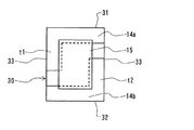
以下において、図面に基づいて本発明の実施形態を詳説する。図1は、本実施形態のチップ抵抗器において、チップ基板30に、上部第1電極14aと、上部第2電極14bと、抵抗体15とが形成された状態を示した概略模式図である。
Hereinafter, embodiments of the present invention will be described in detail with reference to the drawings. FIG. 1 is a schematic diagram showing a state in which an upper
チップ基板30は、一組の互いに平行な第1側縁31と第2側縁32と、これらの第1側縁31と第2側縁32とそれぞれ直交状態となる一組の互いに平行な第3側縁33と第4側縁34とを備えた平面視矩形状のセラミックス製平板であり、後述するようにセラミックス製の大判基板から分割して形成されるものである。
The
上部第1電極14aは、チップ基板30の第1側縁31に沿って設けており、上部第2電極14bは、チップ基板30の第2側縁31に沿って設けておいる。
The upper
特に、上部第1電極14aには、第3側縁33に沿って上部第2電極14b側に突出させた第1突出部t1を設け、上部第2電極14bには、第4側縁34に沿って上部第1電極14a側に突出させた第2突出部t2を設けて、上部第1電極14a及び上部第2電極14bはそれぞれ略L字状としている。
In particular, the upper
抵抗体15は、抵抗体ペーストを略矩形形状にスクリーン印刷によって塗布し、焼成して形成しており、一端を上部第1電極14aに重ね合わせるとともに、他端を上部第2電極14bに重ね合わせ、さらに、抵抗体15の側縁部分を第1突出部t1に重ね合わせるとともに、抵抗体15の側縁部分を第2突出部t2にも重ね合わせている。
The
このように抵抗体15を設けることによって、抵抗体15と上部第1電極14aの接触領域、及び抵抗体15と上部第2電極14bの接触領域を略L字状として接触面積を大きくすることができ、接触面積の増大にともなって抵抗体15の抵抗値を低下させることができる。
By providing the
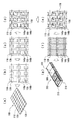
以下において、図2を用いながら本実施形態のチップ抵抗器の製造工程を説明する。本実施形態のチップ抵抗器は、図2(a)に示すように、セラミックス製の大判基板10を用いて製造しているものであって、この大判基板10には、互いに平行な複数の第1溝11と、この第1溝11と直交する複数の第2溝12とを設けて矩形状としたチップ基板領域13を形成している。
Hereinafter, the manufacturing process of the chip resistor of the present embodiment will be described with reference to FIG. As shown in FIG. 2A, the chip resistor according to the present embodiment is manufactured using a ceramic large-
次いで、大判基板10の上面には、スクリーン印刷によって電極ペーストを所定位置に印刷し、印刷された電極ペーストを焼結させて、図2(b)に示すように、各チップ基板領域13に上部第1電極14aと上部第2電極14bを形成している。
Next, on the upper surface of the large-
特に、上部第1電極14aには、第2溝12に沿って上部第2電極14b側に突出させた第1突出部t1を形成しているとともに、上部第2電極14bには、第2溝12に沿って上部第1電極14a側に突出させた第2突出部t2を形成し、上部第1電極14aと上部第2電極14bは略L字状としている。
In particular, the upper
本実施形態では、第1溝11を跨いで電極ペーストを塗布しており、第1溝11を挟んで隣り合った一方のチップ基板領域13の上部第1電極14aと、他方のチップ基板領域13の上部第2電極14bとを一体的に形成している。電極ペーストには銀粉末を配合しており、上部第1電極14a及び上部第2電極14bはそれぞれ銀電極としている。
In the present embodiment, the electrode paste is applied across the
図示しないが、大判基板10の下面にも同様にスクリーン印刷によって電極ペーストを所定位置に印刷し、印刷された電極ペーストを焼結させて下部第1電極14c及び下部第2電極14dを形成している(図2(g)参照)。
Although not shown, an electrode paste is similarly printed on the lower surface of the large-
各電極14a,14b,14c,14dの形成後、各チップ基板領域13中の上部第1電極14aと上部第2電極14bとの間には、スクリーン印刷によって抵抗体ペーストを矩形状に印刷し、印刷された抵抗体ペーストを焼結させて、図2(c)に示すように、各チップ基板領域13に抵抗体15を形成している。本実施形態では、抵抗体ペーストはルテニウムを主原料としている。
After each
特に、抵抗体15となる抵抗体ペーストは、上部第1電極14aの第1突出部t1、及び上部第2電極14bの第2突出部t2に重ね合わせながら塗布していることによって、第1突出部t1及び第2突出部t2によって抵抗体ペーストが流れ広がることを防止できるので、厚膜状に抵抗体15を形成することができる。
In particular, the resistor paste used as the
抵抗体15の形成後、各チップ基板領域13中の抵抗体15の上面には、スクリーン印刷によってガラスペーストを所定形状に印刷し、印刷されたガラスペーストを焼結させて、図2(d)に示すように、各チップ基板領域13に抵抗体15を被覆した保護ガラス層16を形成している。
After the
保護ガラス層16の形成後、図示しないプローブをそれぞれ上部第1電極14a及び上部第2電極14bに当接させて、抵抗体15の電流値または電圧値を計測しながら抵抗体15をレーザートリミングして、抵抗体15の抵抗値調整を行っている。図2(e)中、17はレーザートリミングによって抵抗体15に刻まれたトリミング溝である。
After the
特に、トリミングを行う場合には、図2(e)に示すように、第2突出部t2の上部第1電極14a側端部と上部第1電極14aとの間を開始点としてトリミング溝17を形成することにより、トリミング溝17を確実に形成できるので、確実な抵抗値調整を行うことができる。なお、第1突出部t1の上部第2電極14b側端部と上部第2電極14bとの間を開始点としてトリミング溝17を形成してもよい。
In particular, when trimming is performed, as shown in FIG. 2E, a trimming
レーザートリミングによる抵抗値調整後、図2(f)に示すように保護ガラス層16の上面にはガラスペーストまたは樹脂ペーストを印刷して硬化させることによりオーバーコート層18を形成し、抵抗体15を絶縁被覆している。なお、オーバーコート層18の形成前に、抵抗体15の上面にガラスペーストなどを薄く印刷して焼結させることによりトリミング溝17の埋め戻しを行ってもよい。
After adjusting the resistance value by laser trimming, an
オーバーコート層18の形成後、第1溝11に沿って大判基板10を分割することにより、図2(g)に示すようにチップ基板30が一列に連なったバー状基板20を形成している。第1溝11に沿った大判基板10の分割により、チップ基板30の第1側縁31と第2側縁32とが形成されている。
After the
大判基板10をバー状基板20に分割した後、分割にともなって露出したバー状基板20の露出面には、電極ペーストをそれぞれ塗布して焼結させることにより上部第1電極14aと下部第1電極14cとを電気的に接続する第1側面電極(図示せず)と、上部第2電極14bと下部第2電極14dとを電気的に接続する第2側面電極(図示せず)を形成している。
After dividing the large-
第1側面電極と第2側面電極の形成後、第2溝12に沿ってバー状基板20を分割することにより個々のチップ基板30とし、このチップ基板にはバレルめっき処理を行うことにより、図2(h)に示すように、第1側面電極部分及び第2側面電極部分にめっき被膜35を形成し、チップ抵抗器としている。めっき被膜35は、ニッケルめっき被膜と半田めっき被膜の積層構造としている。第2溝12に沿ったバー状基板20の分割により、チップ基板30の第3側縁33と第4側縁34とが形成されている。
After the formation of the first side electrode and the second side electrode, the bar-shaped
前述したようにチップ抵抗器を形成することによって、50mΩ以下のチップ抵抗器を極めて精度よく形成することができる。本実施形態では、1つのチップ基板30に1つの抵抗体15を設けたチップ抵抗器について説明したが、1つのチップ基板に複数の抵抗体を設けた多連チップ抵抗器の場合にも、電極を同様に形成することによって低抵抗値の多連チップ抵抗器とすることができる。
By forming the chip resistor as described above, a chip resistor of 50 mΩ or less can be formed with extremely high accuracy. In the present embodiment, the chip resistor in which one
前述した実施形態では、図2(b)に示すように、各チップ基板領域13には、上部第1電極14aと上部第2電極14bとをそれぞれ同一パターンで形成しているが、例えば、図3に示すように、上部第1電極14aと上部第2電極14bは、第2溝12を鏡面対称軸として、第2溝12を挟んで隣接したチップ基板領域13に、鏡面対称となるパターンで形成してもよい。
In the embodiment described above, the upper
このような鏡面対称となるパターンで上部第1電極14aと上部第2電極14bとを形成した場合には、第2溝12を挟んで隣接した上部第1電極14aの第1突出部t1、及び第2溝12を挟んで隣接した上部第2電極14bの第2突出部t2を、第2溝12を挟んでそれぞれ一体的に形成することができる。
When the upper
したがって、第1突出部t1及び第2突出部t2の突出方向と直交する方向における幅寸法を小さくしても、第1突出部t1及び第2突出部t2をそれぞれ確実に形成できる。 Therefore, even if the width dimension in the direction orthogonal to the protruding direction of the first protruding portion t1 and the second protruding portion t2 is reduced, the first protruding portion t1 and the second protruding portion t2 can be reliably formed.
特に、第2溝12を挟んで一体的に形成した第1突出部t1及び第2突出部t2は、電極ペーストを塗布・焼成して形成した際に、より高い盛り上がり形状とすることができるので、第1突出部t1の上面及び第2突出部t2の上面に抵抗体ペーストを塗布した場合に、抵抗体ペーストが流れ広がることを抑制しやすく、抵抗体15をより厚膜状に形成することができる。
In particular, since the first protrusion t1 and the second protrusion t2 formed integrally with the
10 大判基板
11 第1溝
12 第2溝
13 チップ基板領域
14a 上部第1電極
14b 上部第2電極
14c 下部第1電極
14d 下部第2電極
15 抵抗体
16 保護ガラス層
17 トリミング溝
18 オーバーコート層
20 バー状基板
30 チップ基板
31 第1側縁
32 第2側縁
33 第3側縁
34 第4側縁
35 めっき被膜
t1 第1突出部
t2 第2突出部
10 Large format board
11 1st groove
12 Second groove
13 Chip substrate area
14a Upper first electrode
14b Upper second electrode
14c Lower first electrode
14d Lower second electrode
15 resistor
16 Protective glass layer
17 Trimming groove
18 Overcoat layer
20 Bar substrate
30 chip substrate
31 First side edge
32 Second side edge
33 3rd side edge
34 4th side edge
35 Plating film
t1 First protrusion
t2 Second protrusion
Claims (2)
このチップ基板上面に、前記第1側縁及び前記第2側縁に沿って設けたそれぞれ上部第1電極及び上部第2電極と、
この上部第1電極と上部第2電極とにそれぞれ両端を重ね合わせながら前記チップ基板の上面に設けた抵抗体と
を備えたチップ抵抗器において、
前記上部第1電極には、前記第3側縁に沿って前記上部第2電極側に突出させた第1突出部を設け、
前記上部第2電極には、前記第4側縁に沿って前記上部第1電極側に突出させた第2突出部を設け、
前記抵抗体は、側縁部分を前記第1突出部と前記第2突出部とに重ね合わせて配置したことを特徴とするチップ抵抗器。 A set of mutually parallel first and second side edges, and a set of mutually parallel third and fourth side edges that are orthogonal to the first and second side edges respectively. A rectangular chip substrate in plan view with
An upper first electrode and an upper second electrode provided on the upper surface of the chip substrate along the first side edge and the second side edge, respectively;
In a chip resistor comprising a resistor provided on the upper surface of the chip substrate while overlapping both ends of the upper first electrode and the upper second electrode,
The upper first electrode is provided with a first protrusion that protrudes toward the upper second electrode along the third side edge,
The upper second electrode is provided with a second protrusion that protrudes toward the upper first electrode along the fourth side edge,
The resistor is a chip resistor, wherein a side edge portion is disposed so as to overlap the first protrusion and the second protrusion.
Priority Applications (1)
| Application Number | Priority Date | Filing Date | Title |
|---|---|---|---|
| JP2005355802A JP2007165358A (en) | 2005-12-09 | 2005-12-09 | Chip-type capacitor |
Applications Claiming Priority (1)
| Application Number | Priority Date | Filing Date | Title |
|---|---|---|---|
| JP2005355802A JP2007165358A (en) | 2005-12-09 | 2005-12-09 | Chip-type capacitor |
Publications (1)
| Publication Number | Publication Date |
|---|---|
| JP2007165358A true JP2007165358A (en) | 2007-06-28 |
Family
ID=38247981
Family Applications (1)
| Application Number | Title | Priority Date | Filing Date |
|---|---|---|---|
| JP2005355802A Pending JP2007165358A (en) | 2005-12-09 | 2005-12-09 | Chip-type capacitor |
Country Status (1)
| Country | Link |
|---|---|
| JP (1) | JP2007165358A (en) |
Cited By (2)
| Publication number | Priority date | Publication date | Assignee | Title |
|---|---|---|---|---|
| JP2017126593A (en) * | 2016-01-12 | 2017-07-20 | パナソニックIpマネジメント株式会社 | Chip resistor |
| JP2018139248A (en) * | 2017-02-24 | 2018-09-06 | パナソニックIpマネジメント株式会社 | Mounting structure of chip resistor |
Citations (6)
| Publication number | Priority date | Publication date | Assignee | Title |
|---|---|---|---|---|
| JPS61149304U (en) * | 1985-03-06 | 1986-09-16 | ||
| JPS63213301A (en) * | 1987-02-28 | 1988-09-06 | イビデン株式会社 | Printed wiring board with printed resistor |
| JPH077102U (en) * | 1993-06-29 | 1995-01-31 | 京セラ株式会社 | Fixed resistor |
| JPH09148703A (en) * | 1995-11-29 | 1997-06-06 | Fujitsu Ltd | Thick film resistor and method for adjusting resistance value of it |
| JP2002237401A (en) * | 2001-02-13 | 2002-08-23 | Matsushita Electric Ind Co Ltd | Resistor |
| JP2002270402A (en) * | 2001-03-09 | 2002-09-20 | Rohm Co Ltd | Chip resistor |
-
2005
- 2005-12-09 JP JP2005355802A patent/JP2007165358A/en active Pending
Patent Citations (6)
| Publication number | Priority date | Publication date | Assignee | Title |
|---|---|---|---|---|
| JPS61149304U (en) * | 1985-03-06 | 1986-09-16 | ||
| JPS63213301A (en) * | 1987-02-28 | 1988-09-06 | イビデン株式会社 | Printed wiring board with printed resistor |
| JPH077102U (en) * | 1993-06-29 | 1995-01-31 | 京セラ株式会社 | Fixed resistor |
| JPH09148703A (en) * | 1995-11-29 | 1997-06-06 | Fujitsu Ltd | Thick film resistor and method for adjusting resistance value of it |
| JP2002237401A (en) * | 2001-02-13 | 2002-08-23 | Matsushita Electric Ind Co Ltd | Resistor |
| JP2002270402A (en) * | 2001-03-09 | 2002-09-20 | Rohm Co Ltd | Chip resistor |
Cited By (2)
| Publication number | Priority date | Publication date | Assignee | Title |
|---|---|---|---|---|
| JP2017126593A (en) * | 2016-01-12 | 2017-07-20 | パナソニックIpマネジメント株式会社 | Chip resistor |
| JP2018139248A (en) * | 2017-02-24 | 2018-09-06 | パナソニックIpマネジメント株式会社 | Mounting structure of chip resistor |
Similar Documents
| Publication | Publication Date | Title |
|---|---|---|
| US7782173B2 (en) | Chip resistor | |
| US7782174B2 (en) | Chip resistor | |
| US20130222106A1 (en) | Chip thermistor and thermistor assembly board | |
| KR20060002939A (en) | Chip resistor and method for manufacturing same | |
| JP2005026525A (en) | Wiring board and method of manufacturing the same | |
| US8854175B2 (en) | Chip resistor device and method for fabricating the same | |
| JP2000306711A (en) | Multiple chip resistor and production thereof | |
| JP2007165358A (en) | Chip-type capacitor | |
| JP5166140B2 (en) | Chip resistor and manufacturing method thereof | |
| JP4295035B2 (en) | Manufacturing method of chip resistor | |
| JP2019153712A (en) | Chip resistor | |
| JP2004288808A (en) | Manufacturing method for resistor | |
| JP5135745B2 (en) | Chip component and manufacturing method thereof | |
| JP2007150197A (en) | Chip type electronic component | |
| KR101538416B1 (en) | Chip resistor device and method for fabricating the same | |
| KR101544393B1 (en) | Chip resistor device and method for fabricating the same | |
| JP4676198B2 (en) | Four-terminal resistor manufacturing method and four-terminal resistor | |
| JP2013089655A (en) | Method for manufacturing chip resistor | |
| JP3766663B2 (en) | Manufacturing method of chip parts | |
| JP2002359102A (en) | Laminated chip thermistor and method for manufacturing the same | |
| JPH0497501A (en) | Resistor and its manufacture | |
| JPH11312601A (en) | Chip-like electrical component and its manufacture | |
| JPH1126203A (en) | Resistor and manufacture thereof | |
| JP2000306701A (en) | Multiple-chip resistor and manufacture thereof | |
| JPH11204302A (en) | Resistor |
Legal Events
| Date | Code | Title | Description |
|---|---|---|---|
| A621 | Written request for application examination |
Effective date: 20080704 Free format text: JAPANESE INTERMEDIATE CODE: A621 |
|
| A977 | Report on retrieval |
Effective date: 20100415 Free format text: JAPANESE INTERMEDIATE CODE: A971007 |
|
| A131 | Notification of reasons for refusal |
Free format text: JAPANESE INTERMEDIATE CODE: A131 Effective date: 20100511 |
|
| A02 | Decision of refusal |
Effective date: 20100914 Free format text: JAPANESE INTERMEDIATE CODE: A02 |