JP2007160921A - Printing plate, its manufacturing method, roll printing device including printing plate, and manufacturing method for display device using roll printing device - Google Patents
Printing plate, its manufacturing method, roll printing device including printing plate, and manufacturing method for display device using roll printing device Download PDFInfo
- Publication number
- JP2007160921A JP2007160921A JP2006201254A JP2006201254A JP2007160921A JP 2007160921 A JP2007160921 A JP 2007160921A JP 2006201254 A JP2006201254 A JP 2006201254A JP 2006201254 A JP2006201254 A JP 2006201254A JP 2007160921 A JP2007160921 A JP 2007160921A
- Authority
- JP
- Japan
- Prior art keywords
- printing
- display panel
- ink
- printing plate
- groove
- Prior art date
- Legal status (The legal status is an assumption and is not a legal conclusion. Google has not performed a legal analysis and makes no representation as to the accuracy of the status listed.)
- Withdrawn
Links
Images


Classifications
-
- B—PERFORMING OPERATIONS; TRANSPORTING
- B41—PRINTING; LINING MACHINES; TYPEWRITERS; STAMPS
- B41M—PRINTING, DUPLICATING, MARKING, OR COPYING PROCESSES; COLOUR PRINTING
- B41M1/00—Inking and printing with a printer's forme
-
- G—PHYSICS
- G02—OPTICS
- G02F—OPTICAL DEVICES OR ARRANGEMENTS FOR THE CONTROL OF LIGHT BY MODIFICATION OF THE OPTICAL PROPERTIES OF THE MEDIA OF THE ELEMENTS INVOLVED THEREIN; NON-LINEAR OPTICS; FREQUENCY-CHANGING OF LIGHT; OPTICAL LOGIC ELEMENTS; OPTICAL ANALOGUE/DIGITAL CONVERTERS
- G02F1/00—Devices or arrangements for the control of the intensity, colour, phase, polarisation or direction of light arriving from an independent light source, e.g. switching, gating or modulating; Non-linear optics
- G02F1/01—Devices or arrangements for the control of the intensity, colour, phase, polarisation or direction of light arriving from an independent light source, e.g. switching, gating or modulating; Non-linear optics for the control of the intensity, phase, polarisation or colour
- G02F1/13—Devices or arrangements for the control of the intensity, colour, phase, polarisation or direction of light arriving from an independent light source, e.g. switching, gating or modulating; Non-linear optics for the control of the intensity, phase, polarisation or colour based on liquid crystals, e.g. single liquid crystal display cells
- G02F1/133—Constructional arrangements; Operation of liquid crystal cells; Circuit arrangements
- G02F1/1333—Constructional arrangements; Manufacturing methods
- G02F1/1339—Gaskets; Spacers; Sealing of cells
Landscapes
- Physics & Mathematics (AREA)
- Nonlinear Science (AREA)
- Mathematical Physics (AREA)
- Chemical & Material Sciences (AREA)
- Crystallography & Structural Chemistry (AREA)
- General Physics & Mathematics (AREA)
- Optics & Photonics (AREA)
- Liquid Crystal (AREA)
- Devices For Indicating Variable Information By Combining Individual Elements (AREA)
Abstract
Description
本発明は、ロールプリント装置に係り、より詳しくは、ブレードを用いたロールプリント装置、それを用いたインクパターン形成方法及び液晶表示装置の製造方法に関する。 The present invention relates to a roll printing apparatus, and more particularly, to a roll printing apparatus using a blade, an ink pattern forming method using the roll printing apparatus, and a method for manufacturing a liquid crystal display device.
情報化社会の発展に伴い、表示装置に関する要求も多様な形態に変化している。従来テレビジョンやコンピュータモニタなどの表示装置に多く使用された陰極線管に代わり、大型化、平面化、スリム化などの要求に合致する液晶表示装置、有機EL表示装置、電界放出表示装置、プラズマ表示装置などの多様な平板表示装置が開発され活用されている。 With the development of the information society, the demands on display devices are changing in various forms. Instead of cathode ray tubes that have been widely used in conventional display devices such as televisions and computer monitors, liquid crystal display devices, organic EL display devices, field emission display devices, and plasma displays that meet the demands for large size, flattening, slimming, etc. Various flat panel display devices such as devices have been developed and utilized.
平板表示装置は、相異なる機能を有する対向配置された第1及び第2の表示板を含む。第1及び第2の表示板は、所定間隔で離隔され配置されている。第1の表示板と第2の表示板との間には、前記間隔を一定に維持するスペーサが備えられている。 The flat panel display includes first and second display panels arranged to face each other and having different functions. The first and second display panels are spaced apart from each other at a predetermined interval. A spacer is provided between the first display panel and the second display panel to maintain the spacing constant.
前記スペーサとしては、ビーズスペーサとカラムスペーサとが使用されている。ビーズスペーサは、主として散布法を用いて形成する。散布法は、工程が単純で低コストであるが、スペーサの散布位置を精密に制御しにくく、ビーズスペーサを画素領域に散布する場合、画質を低下させてしまう。 As the spacer, a bead spacer and a column spacer are used. The bead spacer is formed mainly using a spraying method. The spraying method is simple and low-cost, but it is difficult to precisely control the spacer spraying position, and when the bead spacers are sprayed on the pixel area, the image quality is degraded.
カラムスペーサは、主として有機物をフォトエッチング工程によってパターニングすることによって形成するので、位置制御に有利である。しかしながら、工程が複雑になり、工程時間及びコストが増加するようになる。 Since the column spacer is mainly formed by patterning an organic substance by a photoetching process, it is advantageous for position control. However, the process becomes complicated, and the process time and cost increase.
最近、上述した散布法及びフォトエッチング法に代わるスペーサ形成方法であるロールプリント装置を用いた印刷法が研究されている。ロールプリント装置を用いた印刷法は、製造工程が単純で製造時間を短縮でき、低コスト化が実現できる。 Recently, a printing method using a roll printing apparatus, which is a spacer forming method instead of the above-described spraying method and photoetching method, has been studied. A printing method using a roll printing apparatus has a simple manufacturing process, can reduce manufacturing time, and can realize cost reduction.
前記印刷法は、散布法に比べて比較的正確な位置にスペーサアレイを形成できるが、転写シートの特性によって転写誤差が発生する場合がある。このような誤差は、基板が大型化され、ロールプリント装置に備えられた転写ローラのローリング距離が長くなるに従って、さらに大きくなる。このような誤差によってスペーサが正確な位置に形成されないと、セルギャップを効果的に維持することができなくなる。そして、誤差が累積され画素領域に形成される場合、開口率を減少させるなど画質を低下させるようになる。
本発明が解決しようとする技術的課題は、大型基板上においても精密なインクパターン形成が可能なロールプリント装置を提供することにある。 A technical problem to be solved by the present invention is to provide a roll printing apparatus capable of forming a precise ink pattern even on a large substrate.
本発明が解決しようとする他の技術的課題は、前記ロールプリント装置に用いる印刷版を提供することにある。 Another technical problem to be solved by the present invention is to provide a printing plate for use in the roll printing apparatus.
本発明が解決しようとするさらに他の技術的課題は、前記印刷版の製造方法を提供することにある。 Still another technical problem to be solved by the present invention is to provide a method for producing the printing plate.
本発明が解決しようとする他の技術的課題は、前記ロールプリント装置を用いた表示装置の製造方法を提供することにある。 Another technical problem to be solved by the present invention is to provide a method of manufacturing a display device using the roll printing apparatus.
本発明の技術的課題は、上述した技術的課題に制限されるわけではなく、言及されないまたは他の技術的課題は以下の記載から当業者に明確に理解される。 The technical problems of the present invention are not limited to the technical problems described above, and other technical problems that are not mentioned or will be clearly understood by those skilled in the art from the following description.
前記技術的課題を達成するための本発明の一実施形態によるロールプリント装置は、第1の方向に沿って等間隔に配列されており、前記第1の方向と垂直な第2の方向の開始列より終了列において間隔が広く配列されており、2枚の互いに対向する基板を含む表示パネルのセルギャップと深さが実質的に同一な複数の印刷溝アレイを含む印刷版と、前記印刷溝に充填されたインクを前記表示パネルの一方の基板に転写する転写シートを備える転写ローラとを含む。 A roll printing apparatus according to an embodiment of the present invention for achieving the technical problem is arranged at equal intervals along a first direction, and starts in a second direction perpendicular to the first direction. A printing plate including a plurality of print groove arrays having a substantially equal cell gap and depth in a display panel including two substrates facing each other, wherein the print grooves are arranged wider in an end row than in a row; And a transfer roller provided with a transfer sheet for transferring the ink filled in to the one substrate of the display panel.
前記他の技術的課題を達成するための本発明の一実施形態による印刷版は、2枚の互いに対向する基板を含む表示パネルのセルギャップと深さが実質的に同一な複数の印刷溝アレイを備える印刷版であって、前記印刷溝は、第1の方向に沿って等間隔に配列されており、前記第1の方向と垂直な第2の方向に沿って開始列より終了列において間隔が広く配列されている。 According to another aspect of the present invention, there is provided a printing plate comprising a plurality of printed groove arrays having substantially the same cell gap and depth as a display panel including two opposing substrates. The printing grooves are arranged at equal intervals along a first direction, and are spaced from a start row to an end row along a second direction perpendicular to the first direction. Are widely arranged.
前記さらに他の技術的課題を達成するための本発明の一実施形態による印刷版の製造方法は、2枚の互いに対向する基板を含む表示パネルのスペーサアレイと同一な間隔を有するテスト印刷版の凹溝アレイにインクを充填することと、前記テスト印刷版上に転写シートを備える転写ローラをローリングすることによってインクを前記転写シートに転写することと、前記転写シートに転写されたインクをテスト基板上に再転写することと、前記再転写されたインクパターンの間隔と前記スペーサアレイの間隔とを比較することによって印刷溝アレイの間隔を決定することを含む。 According to another aspect of the present invention, there is provided a method of manufacturing a printing plate according to an embodiment of the present invention, wherein a test printing plate having the same spacing as a spacer array of a display panel including two opposing substrates is provided. Filling the groove array with ink, rolling a transfer roller having a transfer sheet on the test printing plate to transfer the ink to the transfer sheet, and transferring the ink transferred to the transfer sheet to the test substrate Re-transferring up and determining the spacing of the print groove arrays by comparing the spacing of the re-transferred ink pattern with the spacing of the spacer array.
前記さらに他の技術的課題を達成するための本発明の一実施形態による表示装置の製造方法は、第1の方向に沿って等間隔に配列されており、前記第1の方向と垂直な第2の方向の開始点より終了点において間隔が広く配列されており、2枚の互いに対向する基板を含む表示パネルのセルギャップと深さが実質的に同一な印刷版の印刷溝アレイにスペーサを含むインクを充填すること、前記印刷版上に転写シートを備える転写ローラをローリングすることによって前記インクを前記転写シートに転写すること、及び前記転写シートに転写されたインクを前記表示パネルの一方の基板上に再転写することを含む。 A method of manufacturing a display device according to an embodiment of the present invention for achieving the further technical problem is arranged in a first direction perpendicular to the first direction, arranged at equal intervals along the first direction. The spacers are arranged in the printing groove array of the printing plate having the same gap between the cell gap and the depth of the display panel including two substrates facing each other. Filling the ink containing, transferring the ink to the transfer sheet by rolling a transfer roller having a transfer sheet on the printing plate, and transferring the ink transferred to the transfer sheet to one of the display panels Re-transferring onto a substrate.
その他実施形態の具体的な事項は、詳細な説明及び図面に含まれている。 Specific matters of the other embodiments are included in the detailed description and the drawings.
上述したように本発明の実施形態によるロールプリント装置によれば、大型基板上においても精密なパターン間隔を有するインクパターンの形成が可能となる。また、前記ロールプリント装置を用いて表示装置のスペーサアレイを形成すれば、スペーサアレイが遮光領域に正確に配置されるので、開口率が向上し、且つセルギャップの精度を改善することができる。 As described above, according to the roll printing apparatus according to the embodiment of the present invention, it is possible to form an ink pattern having a precise pattern interval even on a large substrate. Further, when the spacer array of the display device is formed using the roll printing device, the spacer array is accurately arranged in the light shielding region, so that the aperture ratio can be improved and the accuracy of the cell gap can be improved.
本発明の利点及び特徴、そしてそれらを達成する方法は添付する図面と共に詳細に後述する実施形態を参照すれば明確になる。しかしながら、本発明は、以下開示する実施形態に限定されるわけではなく、相異なる多様な形態で実現される。本実施形態は、本発明の開示が完全となり、当業者に発明の範疇を完全に知らせるために提供されるものである。本発明は、特許請求の範囲の記載に基づいて解釈されなければならない。図面において、層及び領域の大きさ及び相対的な大きさは、説明の便宜上、誇張されて表現されている場合がある。 Advantages and features of the present invention and methods for achieving them will be apparent with reference to the embodiments described below in detail with reference to the accompanying drawings. However, the present invention is not limited to the embodiments disclosed below, and can be realized in various different forms. This embodiment is provided so that the disclosure of the present invention will be complete and those skilled in the art will be fully informed of the scope of the invention. The present invention should be construed based on the description of the claims. In the drawings, the sizes and relative sizes of layers and regions may be exaggerated for convenience of explanation.
素子又は層が他の素子又は層の“上方(over)”又は“上(on)”に指称されることは、他の素子又は層の真上だけではなく、中間に他の層又は他の素子を介在した場合を全て含む。反面、素子が“直接上”又は“真上”に指称されることは、中間に他の素子又は層を介在しないことを示す。なお、明細書全体にかけて同一参照符号は同一構成要素を示すものとする。“及び/又は”は、言及されたアイテムのそれぞれ及び一つ以上の全ての組合を含む。 An element or layer is referred to as “over” or “on” over another element or layer, not just directly over another element or layer, All cases where an element is interposed are included. On the other hand, designation of an element “directly above” or “directly above” indicates that no other element or layer is interposed in between. Note that the same reference numerals denote the same components throughout the specification. “And / or” includes each and every combination of one or more of the items mentioned.
以下、添付した図面を参照して本発明の好適な一実施形態によるロールプリント装置について詳細に説明する。 Hereinafter, a roll printing apparatus according to a preferred embodiment of the present invention will be described in detail with reference to the accompanying drawings.
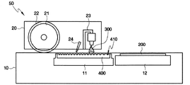
図1は、本発明の一実施形態によるロールプリント装置の概略的な断面図である。 FIG. 1 is a schematic cross-sectional view of a roll printing apparatus according to an embodiment of the present invention.
図1を参照する。ロールプリント装置50は表示板上に多様なインクパターンを印刷する場合に使用される装置であって、印刷版400と印刷版400に充填されたインクを表示板上に転写する転写ローラ21を含む。ロールプリント装置50によって印刷することができるインクパターンの種類は数多いが、以下では表示装置の表示パネル間セルギャップを維持するためのスペーサアレイを形成する場合を例に挙げて説明する。
Please refer to FIG. The
印刷版400は、目的とする対象パターンであるスペーサアレイを形成するための多数の印刷溝410アレイを備える。ここで、印刷溝410アレイの一つの印刷溝410は、スペーサアレイの一つのスペーサに対応する。一つのスペーサは、一つの単位スペーサからなるようにしてもよいが、それに制限されるわけではなく、多数の単位スペーサの集合からなるようにしてもよい。印刷溝410アレイについてのより詳細な説明は後述する。
The
印刷版400は、下部フレーム10に設けられている印刷版支持台11によって収納される。下部フレーム10には、印刷版支持台11と並んで基板支持台12が設けられている。基板支持台12には表示板などの対象基板が設置され、ここでインク印刷が行われる。
The
印刷版400の上側には、転写ローラ21が設けられている。転写ローラ21は、例えば円筒形でなるようにしてもよい。転写ローラ21の外面は、転写シート22で覆われている。転写シート22は、インク300との付着性に優れた材質からなり、例えば親水性に優れたシリコンを含むようにしてもよい。転写シート22には、印刷版400からの転写及び表示板への再転写が容易となるように、弾性を有するものを用いるか、或いは硬度が小さいものを用いるようにすればよい。
A
転写ローラ21は、下部フレーム10の上で下部フレーム10と相対的に往復運動する上部フレーム20に設けられている。例えば、下部フレーム10が固定された状態で、上部フレーム20が下部フレーム10上を往復運動する。この時、転写ローラ21が回転しながら、転写ローラ21を覆っている転写シート22が、印刷版400の上面及び/又は表示板200の上面と接触するように上部フレーム20の位置を下部フレーム10に近接するように調節する。一方、転写ローラ21の転写シート22が表示板200の上面に必ずしも接触する必要はないが、少なくとも印刷版400から転写シート22に転写されたインクが表示板200の上面に触れることができる程度の距離を維持する必要がある。
The
上部フレームがインク供給装置23及びブレード24をさらに含むようにしてもよい。インク供給装置23及び/又はブレード24は、インク300が転写される時の転写ローラ21のローリング方向に対して転写ローラ21の前側に設けられるようにしてもよい。
The upper frame may further include an
ブレード24は、インク供給装置23の後側に設けられ、印刷溝410アレイの幅に対応する広い幅を有している。ブレード24は、印刷溝410アレイにインク300を充填し、印刷版400上面に残留するインク300を除去する。
The
以下、本発明の一実施形態によるロールプリント装置及びそれに含まれた印刷版を用いて表示装置を製造する方法について説明する。以下では、前記製造方法が適用される表示装置として液晶表示装置を例にとって説明しているが、本発明はそれに制限されるわけではなく、FED、有機EL表示装置、PDP装置などにも適用できることはいうまでもない。 Hereinafter, a roll printing apparatus according to an embodiment of the present invention and a method for manufacturing a display device using a printing plate included therein will be described. In the following, a liquid crystal display device is described as an example of a display device to which the manufacturing method is applied. However, the present invention is not limited thereto, and can be applied to an FED, an organic EL display device, a PDP device, and the like. Needless to say.
先ず本発明の一実施形態による方法で製造された液晶表示装置の液晶表示パネルについて説明する。図2は、本発明の一実施形態による方法で製造された液晶表示パネルの断面図である。 First, a liquid crystal display panel of a liquid crystal display device manufactured by a method according to an embodiment of the present invention will be described. FIG. 2 is a cross-sectional view of a liquid crystal display panel manufactured by a method according to an embodiment of the present invention.
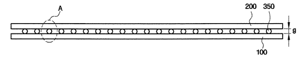
図2を参照すれば、液晶表示装置において画像を表示する液晶表示パネルは、第1の表示板100、それに対向する第2の表示板200及び第1の表示板100と第2の表示板200との間に設けられた液晶層(図示せず)を含む。第1の表示板100と第2の表示板200とは、セルギャップ(g)を維持し、平行に対向配置されている。第1の表示板100と第2の表示板200との間の液晶層にはセルギャップ(g)を維持するためのスペーサ350アレイが配置されている。
Referring to FIG. 2, the liquid crystal display panel displaying an image in the liquid crystal display device includes a
図3は、図2のA部分の拡大図である。以下、図3を参照して本発明の一実施形態による方法で製造された液晶表示パネルについてさらに詳細に説明する。 FIG. 3 is an enlarged view of a portion A in FIG. Hereinafter, the liquid crystal display panel manufactured by the method according to an embodiment of the present invention will be described in more detail with reference to FIG.
図3に示すように、第1の表示板100は、透明なガラス、プラスチックなどからなる第1の絶縁基板110上に形成された多数の配線パターンを含む。具体的には、第1の絶縁基板110上には、アルミニウム(Al)、銅(Cu)、銀(Ag)、モリブデン(Mo)、クロム(Cr)、チタン(Ti)、タンタル(Ta)又はこれらの合金などの導電性物質からなるゲート電極126が形成されている。ゲート電極126上には、窒化シリコン(SiNx)などからなるゲート絶縁膜130が第1の絶縁基板110の全面を覆っている。ゲート絶縁膜130上には、水素化非晶質シリコンなどの半導体からなる半導体層140が形成されている。半導体層140は、少なくとも一部がゲート電極126と重畳されるように設けられている。半導体層140上には、n型不純物が高濃度にドーピングされたn+水素化非晶質シリコンなどからなるオーミックコンタクト層155、156が形成されている。
As shown in FIG. 3, the
オーミックコンタクト層155、156上には、アルミニウム(Al)、銅(Cu)、銀(Ag)、モリブデン(Mo)、クロム(Cr)、チタン(Ti)、タンタル(Ta)又はこれらの合金などの導電性物質からなるソース電極165とドレイン電極166が互いに分離されて設けられている。
On the ohmic contact layers 155 and 156, aluminum (Al), copper (Cu), silver (Ag), molybdenum (Mo), chromium (Cr), titanium (Ti), tantalum (Ta), or alloys thereof are used. A
前述したゲート電極126、半導体層140、ソース電極165及びドレイン電極166は、画素電極180をスイッチングする薄膜トランジスタを構成する。ここで、ゲート電極126は薄膜トランジスタの制御端子を構成し、ソース電極165とドレイン電極166とはそれぞれ薄膜トランジスタの入力端子及び出力端子を構成する。半導体層140は、薄膜トランジスタのチャネル領域を形成する。一方、オーミックコンタクト層155、156は、ソース電極165及びドレイン電極166の分離形状と類似に分離されるように形成されてソース電極165及びドレイン電極166と下部の半導体層140の間の接触抵抗を減らしてやる役割を果たす。
The
ソース電極165及びドレイン電極166上には、窒化シリコン、酸化シリコン(SiOx)及び/又は有機物などになった保護膜170が形成されている。保護膜170上には、酸化インジウム錫(Indium Tin Oxide;ITO)、酸化インジウム亜鉛(Indium Zinc Oxide;IZO)などの透明な導電性物質からなる画素電極180が形成されている。画素電極180は、コンタクトホール176を通して薄膜トランジスタのドレイン電極166と電気的に接続され、マトリックス形状に配列される。
On the
また、図示しないが、画素電極180上には配向膜を形成するようにしてもよい。
Although not shown, an alignment film may be formed on the
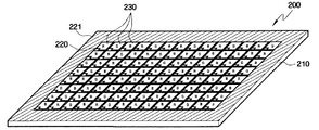
次に、第2の表示板200について説明する。透明なガラス、プラスチックなどからなる第2の絶縁基板210上には、クロム(Cr)などの不透明金属又はカーボンブラックなどを含む不透明有機物などからなる遮光パターン220が形成されている。遮光パターン220は、格子状に形成されており、画素を定義する。画素は遮光パターン220によって定義されており、マトリクス状に配列されている。遮光パターン220上には、カラーフィルタ230が形成されている。カラーフィルタ230は、画素領域に充填され、赤色(R)、緑色(G)、又は青色(B)を呈する有機物からなる。それぞれの色は、一定のパターンで反復的に配列されている。カラーフィルタ230上には、これらの段差を緩和するオーバーコート膜240が設けられている。オーバーコート膜240上には、第1の表示板100の画素電極180と共に電界を形成する共通電極250が形成されている。共通電極250上には配向膜を配置するようにしてもよい。
Next, the
第1の表示板100と第2の表示板200との間には、スペーサ350が設けられている。スペーサ350は、第1の表示板100と第2の表示板200とのセルギャップ(g1、g2)を維持する。
A
液晶表示装置は、バックライトなどから射出された光を用いて画像を表示する。液晶パネルにおいては、光を透過する透過域と光を遮る遮光領域が存在する。遮光領域を構成する構成要素としては、第2の表示板200の遮光パターン220、第1の表示板100の薄膜トランジスタ及びそれらに接続された配線を挙げることができる。第2の表示板200のカラーフィルタ230と第1の表示板100の画素電極180とが重畳する領域は、透過領域を構成する。
The liquid crystal display device displays an image using light emitted from a backlight or the like. In a liquid crystal panel, there are a transmission region that transmits light and a light shielding region that blocks light. Examples of the constituent elements constituting the light shielding region include the
また、一つの遮光領域を構成する構成要素としては、上述したスペーサ350を挙げることができる。液晶表示装置においては、十分な開口率の確保が重要となるが、スペーサ350が透過領域に設けられる場合は、開口率が減少することになる。また、スペーサ350が画素領域に設けられる場合は、光リーク現象を誘発することがある。従って、スペーサ350は、遮光領域に配置されることが好ましい。例えば、第2の表示板の遮光パターン220上に配置するようにすればよい。
Moreover, the above-described
一方、液晶表示パネルのセルギャップには、第1及び第2の表示板100、200に備えられた構成要素による段差によって領域毎に多少差が生じる。遮光領域内でも第1の表示板100の薄膜トランジスタが形成された領域におけるセルギャップ(g1)は、薄膜トランジスタが形成されていない領域におけるセルギャップ(g2)より狭くなる。従って、画素毎に同一なセルギャップを維持するためには、スペーサ350が一定の領域に配列される必要がある。第1の表示板100及び第2の表示板200を圧着することによる薄膜トランジスタの衝撃を防止する観点から、スペーサ350は、遮光領域のうち第2の表示板200の遮光パターン220と第1の表示板100の薄膜トランジスタが形成されない領域との間に配置されることが好ましい。
On the other hand, the cell gap of the liquid crystal display panel is slightly different from region to region due to a step due to the components provided in the first and
スペーサ350の形状は、図3及び他の添付した幾つかの図面において、球形状に模式化されて示されているが、柱形状として形成されてもよく、また、これらに制限されるわけではなく、多様な形状を採り得る。また、2以上の球形状の単位スペーサが集まって一つのスペーサを構成するようにしてもよい。
The shape of the
次に、上述したような液晶表示装置の液晶表示パネルの製造方法について説明する。図4〜図6は、本発明の一実施形態による'液晶表示装置の液晶表示パネルの製造方法の工程段階別斜視図である。本発明の一実施形態による液晶表示パネルの製造方法は、第1の表示板を準備する段階、第2の表示板を準備する段階及び第2の表示板上にスペーサアレイを形成する段階を含む。 Next, a method for manufacturing the liquid crystal display panel of the liquid crystal display device as described above will be described. 4 to 6 are perspective views according to process steps of a method of manufacturing a liquid crystal display panel of a liquid crystal display device according to an embodiment of the present invention. A method of manufacturing a liquid crystal display panel according to an embodiment of the present invention includes preparing a first display panel, preparing a second display panel, and forming a spacer array on the second display panel. .
図2、図3及び図4を参照する。先ず、第1の表示板100を準備する。具体的には、ガラスなどからなる第1の絶縁基板110上にアルミニウム(Al)、銅(Cu)、銀(Ag)、モリブデン(Mo)、クロム(Cr)、チタン(Ti)、タンタル(Ta)又はこれらの合金などの導電性物質を形成しパターニングすることによって第1の方向に並んで延長される複数のゲート線122及びゲート線122が拡張されてなるゲート電極126を形成する。続いて、全面に窒化シリコンを形成してゲート絶縁膜130を形成する。次に、水素化非晶質シリコン及びn型不純物が高濃度にドーピングされたn+水素化非晶質シリコンを形成した後、パターニングすることによって半導体層及び半導体層と実質的に同一なパターンを有するオーミックコンタクト層を形成する。次に、導電性物質を形成しパターニングすることによって第2の方向に並んで延長されている複数のデータ線162、データ線162に接続されたソース電極165及びそれと離隔されたドレイン電極166を形成し、下部のオーミックコンタクト層を一部露出させる。続いて、ソース電極165及びドレイン電極166をエッチングマスクとして用いて一部露出されたオーミックコンタクト層をパターニングすることによって下部の半導体層を露出する。次に、窒化シリコンなどを形成してパターニングすることによってコンタクトホール176を備える保護膜170を形成する。次に、保護膜170上にITO又はIZOなどを形成してパターニングして、ドレイン電極166と電気的に接続された画素電極180を形成する。これで第1の基板100が提供される。
Please refer to FIG. 2, FIG. 3 and FIG. First, the
続いて、第2の表示板200を準備する。図5では、図2及び図3に第2の表示板が覆った状態が示されている。以下では、図5に示す状態を基準として方向を言及することがある。これは上述した方向と反対である場合があるが、同一な相対的位置関係を示すことを容易に理解できるものである。
Subsequently, the
図2、図3及び図5を参照する。具体的には、第2の絶縁基板210上にクロム(Cr)などの不透明金属又はカーボンブラックなどを含む不透明有機物を形成しパターニングすることによって遮光パターン220を形成する。この時、第2の絶縁基板210の最外郭部の遮光パターン221は、画素領域の遮光パターン220と比べて広い幅を有するように形成する。次に、感光性赤色レジストを塗布し、露光及び現像して赤色カラーフィルタを形成する。次に、同一な方法で緑色及び青色カラーフィルタを形成する。これで赤色、緑色及び青色のカラーフィルタ230が形成される。引き続き、全面に有機物質及びITO又はIZOなどを順に積層し、オーバーコート膜240及び共通電極250を形成する。これにより、第2の基板200が提供される。
Please refer to FIG. 2, FIG. 3 and FIG. Specifically, an opaque metal such as chromium (Cr) or an opaque organic material including carbon black is formed on the second insulating
図2、図3及び図6を参照する。第2の表示板200の遮光パターン上にスペーサ350アレイを形成する。スペーサ350アレイは、好ましくは、画素の境界毎に一つずつ形成される。すなわち、隣接するスペーサ間の一方向間隔は、隣接する一方向画素間の間隔と同一であり、隣接するスペーサ間の他方向間隔は隣接する他方向画素間の間隔と同一であるようにしてもよい。また、スペーサ350アレイは、多数個の画素毎に一つずつ形成されるようにしてもよい。この段階のスペーサ350アレイ形成方法については、さらに詳細に後述する。
Please refer to FIG. 2, FIG. 3 and FIG. A
次に、スペーサ350アレイが形成された第2の表示板200に第1の表示板100を対向配置し、シーラントなどを第1の表示板100及び/又は第2の表示板200の周辺部に塗布して第1の表示板100と第2の表示板200とを貼り合わせる。次に、第1の表示板100と第2の表示板200との間に液晶分子を注入して液晶層を形成する。一方、液晶層の形成は、第1の表示板100と第2の表示板200とを貼り合わせる前に、第1の表示板100又は第2の表示板200上に滴下され又は散布されて形成されるようにしてもよい。これで、液晶表示装置の液晶表示パネルが完成する。このような液晶表示パネルの外側面に偏光板を設け、バックライトを配置することによって液晶表示装置が完成する。
Next, the
以下、図6に示すような配列を有するスペーサアレイの形成方法についてさらに詳細に説明する。スペーサアレイ形成方法には、本発明の一実施形態によるロールプリント装置を使用することができ、以下に例示される。 Hereinafter, a method for forming a spacer array having the arrangement as shown in FIG. 6 will be described in more detail. A roll printing apparatus according to an embodiment of the present invention can be used for the spacer array forming method, and is exemplified below.
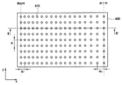
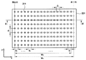
図7は、本発明の一実施形態による液晶表示装置のスペーサアレイ形成方法の工程フロー図である。図8Aは、本発明の一実施形態による印刷版の平面図である。図8Bは、図8AのB−B´線に沿った断面図である。図9〜図12は、本発明の一実施形態による液晶表示装置のスペーサ形成方法の工程段階別断面図である。 FIG. 7 is a process flow diagram of a spacer array forming method for a liquid crystal display device according to an embodiment of the present invention. FIG. 8A is a plan view of a printing plate according to an embodiment of the present invention. 8B is a cross-sectional view taken along line BB ′ of FIG. 8A. 9 to 12 are cross-sectional views according to process steps of the spacer forming method of the liquid crystal display device according to the embodiment of the present invention.
図7及び図8A、図8Bを参照すれる。先ず、印刷版を準備する(S1)。 Please refer to FIG. 7, FIG. 8A, and FIG. 8B. First, a printing plate is prepared (S 1 ).
印刷版400には、印刷溝410アレイが配列されている。印刷溝410の深さ(h)は、スペーサの高さと実質的に同一である。ここで、「実質的に同一」であるという表現の意味は、物理的に完全に同一な場合だけではなく、工程によるマージンや収率によって多少差が生ずる場合を含んでいる。また、上述したように液晶表示パネルのセルギャップは、薄膜トランジスタが設けられている領域にあるかどうかによって多少差が生ずるが、このような誤差は全体のセルギャップに比べて微細なので無視することができる。この場合、各領域におけるセルギャップは、「実質的に同一」であると表現することができる。上述した観点においては、スペーサの高さは、液晶表示パネルのセルギャップと実質的に同一であり、印刷溝の深さは液晶表示パネルのセルギャップと実質的に同一である。
The
一方、後続する工程であるローリング工程において、転写ローラのローリング方向が図8Aの右側行方向(x)であるとき、ローリングによる転写が始まる印刷溝アレイの左側列を「開始列」と定義、転写が終了する印刷溝アレイの右側列を「終了列」と定義する。ここで、印刷溝410アレイは、列方向(y)には一定の同一間隔(d1)を有するが、行方向(x)には一定の間隔を有しない。すなわち、開始列において隣接する各印刷溝410間の行方向間隔(d21)より、終了列における隣接する各印刷溝410間の行方向間隔(d22)がより広くなるように各印刷溝410アレイが配列されている。好ましくは、開始列から終了列に向かうほど行方向間隔が広くなるように配列できる。このような印刷溝410アレイの間隔は、転写ローラのローリング工程によるミスアライン程度を勘案して決定され、これについての詳細な説明は後述する。
On the other hand, in the rolling process, which is a subsequent process, when the rolling direction of the transfer roller is the right row direction (x) in FIG. 8A, the left column of the printing groove array where transfer by rolling starts is defined as the “start column” The right column of the print groove array in which the process ends is defined as an “end column”. Here, the
図7及び図9を参照する。印刷版上にインク供給装置によってインクを供給する(S2)。ここでインク300は、スペーサを含むようにしてもよく、柱形スペーサを形成する場合は、有機物を含むようにしてもよい。
Please refer to FIG. 7 and FIG. Ink is supplied onto the printing plate by an ink supply device (S 2 ). Here, the
図7及び図10を参照する。印刷版のインク溝にインクを充填する(S3)。 Please refer to FIG. 7 and FIG. Ink is filled in the ink groove of the printing plate (S 3 ).
インク300の充填には、ブレード24が用いられる。ここで、説明の便宜のため、印刷溝410アレイの開始列から終了列への方向、すなわち図10で右へ向かう方向を「作業方向」と定義する。図10に示すようにブレード24を印刷版400の上面に接触させた状態で作業方向に移動させれば、印刷版400上面に提供されたインク300が進行方向に押されながら印刷溝410を充填して行く。印刷版400上面のインク300は、ブレード24によって除去される。印刷版400上面の残留インク300の除去を確実にするため、除去用ブレードをさらに備えるようにしてもよい。
A
一方、図10の充填されたインク310の拡大図から分かるように、インクとしてビーズスペーサ301と硬化剤302とを含んだ場合が例示されている。また、一つの印刷溝410に多数の単位ビーズスペーサ301が充填されている。なお、このようなインク310の成分及びそれに含まれるビーズスペーサ301の個数等は、例示したものに限定されるわけではないことは言うまでもない。
On the other hand, as can be seen from the enlarged view of the filled
図7及び図11を参照する。印刷溝に充填されたインクを転写ローラに備えられた転写シートに転写する(S4)。 Please refer to FIG. 7 and FIG. The ink filled in the printing groove is transferred to a transfer sheet provided in the transfer roller (S 4 ).
具体的には、転写シート22が備えられた転写ローラ21をインク310が充填された印刷版400上面でローリングさせる。この時のローリング方向は、前記作業方向と同一である。そうすることによって、印刷溝410に充填されたインク310が転写ローラ21の転写シート22に転写される。
Specifically, the
図7及び図12を参照する。転写シートに転写されたインクを第2の表示板に再転写する(S5)。 Please refer to FIG. 7 and FIG. The ink transferred to the transfer sheet is transferred again to the second display panel (S 5 ).
具体的には、図12に示すようにインク310が転写された転写シート22を備える転写ローラ21を第2の表示板200上でローリングさせる。そうすれば、インク310が第2の表示板200の遮光パターン上に再転写される。インク310が第2の表示板200上に再転写されるとき、転写シート22はある程度の弾性を有しているため、転写圧力を受けるようになり、転写シート22の曲率が変化する。従って、再転写されているインク310と次に再転写されるインク310の間の間隔が短くなるようになる。すなわち、転写ローラ21のローリングによって再転写されるインク310パターンは、転写シート22に転写された各インク310パターン間の間隔又は印刷版400の各印刷溝410アレイの間隔より短くなるようになる。そして、作業方向に異なる印刷溝410間隔を有する印刷版400から転写及び再転写過程を経ながら間隔が補正され、第2の表示板200上ではインク310は一定した間隔に再転写される。ここで、第2の表示板200上に再転写されるインク310パターンの間隔は、印刷版400の印刷溝410アレイの間隔によって決定される。このような印刷溝410アレイの間隔を決定する具体的な方法については後述する。
Specifically, as shown in FIG. 12, the
続いて、必要に応じて第2の表示板200上に再転写されたインク310を硬化させることによってスペーサが完成する。この時、インク供給装置から供給されたインクが硬化剤以外の溶液を含んでいる場合、乾燥などによって単純に溶液を除去することによって単位スペーサのみからなるスペーサを完成するようにしてもよい。また、インクが有機物からなる場合には、熱、光などによる有機物硬化工程を追加的に経るようにすればよい。
Subsequently, the
以下、上述したようなロールプリント装置を用いたスペーサ形成方法に適用される印刷版の製造方法についてさらに詳細に説明する。図13は、本発明の一実施形態による印刷版の製造方法の工程フローである。図14A及び図15Aは、本発明の一実施形態による印刷版の製造方法の工程段階別平面図である。図14B及び図15Bは、それぞれ、図14A及び図15AのB−B´線に沿った断面図である。図16は、本発明の一実施形態による方法で製造された印刷版の平面図である。 Hereinafter, the printing plate manufacturing method applied to the spacer forming method using the roll printing apparatus as described above will be described in more detail. FIG. 13 is a process flow of a printing plate manufacturing method according to an embodiment of the present invention. FIG. 14A and FIG. 15A are plan views according to process steps of a printing plate manufacturing method according to an embodiment of the present invention. 14B and 15B are cross-sectional views taken along the line BB ′ of FIGS. 14A and 15A, respectively. FIG. 16 is a plan view of a printing plate manufactured by a method according to an embodiment of the present invention.
図13及び図14A、図16Bを参照する。先ず、テスト印刷版を準備する(S11)。 Please refer to FIG. 13, FIG. 14A, and FIG. 16B. First, a test printing plate is prepared (S 11 ).
テスト印刷版500は、目的とするスペーサアレイと同一間隔(d2)を有する印刷溝510アレイを備える。すなわち、印刷溝510アレイの列方向(y)間隔(d1)が同一であり、行方向(x)間隔(d2)もまた同一である。
The
続いて、図7〜図12に示す方法と同一な方法によってテスト基板上にインクを印刷する。具体的には、準備したテスト印刷版上にインクを供給する(S12)。インクはスペーサを含むようにしてもよいが、マーキング機能をする物質のみからなるようにしてもよい。次に、ブレードを用いてテスト印刷版500印刷溝510にインクを充填する(S13)。その次に、テスト印刷版500の上面に転写シートを備える転写ローラをローリングすることにより印刷溝に充填されたインクを転写シートに転写する(S14)。
Subsequently, ink is printed on the test substrate by the same method as shown in FIGS. Specifically, ink is supplied onto the prepared test printing plate (S 12 ). The ink may include a spacer, but may include only a substance having a marking function. Next, ink is filled into the
引き続き、転写ローラをテスト基板上にローリングすることにより転写シートに転写されたインクをテスト基板上に再転写する(S15)。テスト基板としては、目的とする第2の表示板と同一形状を有する表示板又は基板を使用するようにすればよい。 Subsequently, the ink transferred to the transfer sheet is re-transferred onto the test substrate by rolling the transfer roller onto the test substrate (S 15 ). As the test substrate, a display plate or a substrate having the same shape as the target second display plate may be used.
図13及び図15A、図15Bを参照する。再転写されたインク311パターンの行方向(x)間隔(bk)と目的とする対象スペーサアレイの間隔(c1)とを比較する(S16)。図15A及び図15Bでは、テスト基板201上に対象スペーサアレイの配列位置が点線に示されている。対象スペーサアレイの行方向(x)間隔(c1)は一定である。一方、テスト基板201上に再転写されたインク311パターンにおいては、転写シートから再転写時発生する転写圧力などによって転写ローラ進行方向である行方向(x)への間隔が一定とはならない。すなわち、図15A及び図15Bに示すように、行方向(x)の間隔がより短くなる。再転写されたインク311パターンの行方向(x)間隔(bk)においては、再転写終了列における間隔(bn)が再転写開始列における間隔(b1)より短くなる。
Please refer to FIG. 13 and FIGS. 15A and 15B. The row direction (x) interval (b k ) of the
このような間隔の変化は、転写シートの材料、厚さなどに依存する。また、このような間隔の変化は、再転写されるインク311パターンの行方向(x)幅がさらに広いほど、すなわち転写ローラのローリング距離が長くなるほど増加する。同一の転写シートを用いて印刷する場合、間隔の変化は転写ローラのローリング距離に比例する。従って、再転写開始列から遠くなるほど間隔は狭くなるようになる。すなわち、図15A及び図15Bでローリング開始列からローリング終了列に向かうほど間隔が狭くなる(bk−1>bk)。
Such a change in the interval depends on the material and thickness of the transfer sheet. Further, such a change in the interval increases as the width in the row direction (x) of the
続いて、図13及び図16を参照する。前記結果に基づいて印刷溝アレイ間隔が補正された印刷版を製造する(S17)。図16の印刷版は、補正された間隔が適用された例が示されている。すなわち、印刷溝410アレイの開始列から終了列に向かうほど印刷溝の間隔が広くなるように配列されている(wk−1<wk)。
Next, refer to FIG. 13 and FIG. A printing plate in which the printing groove array interval is corrected based on the result is manufactured (S 17 ). The printing plate of FIG. 16 shows an example in which corrected intervals are applied. That is, the print groove is arranged so that the interval between the print grooves becomes wider from the start row to the end row of the
以下、上述したような印刷溝アレイ間隔を決定する方法について図15A、図15B及び図16を参照してさらに詳細に説明する。 Hereinafter, a method of determining the print groove array interval as described above will be described in more detail with reference to FIGS. 15A, 15B, and 16. FIG.
先ず、図15A及び図15Bで、対象スペーサアレイの行方向(x)幅(Wt1)と実際再転写されたインクパターンの行方向(x)幅(Wt2)とを測定する。ここで、製造しようとする印刷版の印刷溝アレイの行方向幅(Wp)は次の比例数式(1)を満足するようになる。 First, in FIGS. 15A and 15B, to measure the target spacer array in the row direction (x) width (W t1) and the actual retransferred row direction (x) the width of the ink pattern (W t2). Here, the row direction width (W p ) of the printing groove array of the printing plate to be manufactured satisfies the following proportional expression (1).
![]()
![]()
前記数式(1)において、Wpの値は次の数式(2)の通り計算される。 In the formula (1), the value of W p is calculated as the following formula (2).

一方、製造しようとする印刷版の印刷溝アレイの行方向間隔を開始列からb1、b2、b3、・・・bnとそれぞれ定義し、縮小される間隔が転写ローラのローリング距離に比例し、この時の比例定数をrと定義すれば、bk及びbk+1は次の数式(3)及び(4)を満足する。 On the other hand, the row direction interval of the printing groove array of the printing plate to be manufactured is defined as b 1 , b 2 , b 3 ,..., B n from the start column, and the reduced interval is the rolling distance of the transfer roller. If the proportionality constant at this time is defined as r, b k and b k + 1 satisfy the following equations (3) and (4).
前記数式(3)及び(4)から次の数式(5)及び(6)を得ることができる。 The following formulas (5) and (6) can be obtained from the formulas (3) and (4).
前記数式(3)及び(4)からWpは次の数式(7)で表現できる。 From the equations (3) and (4), W p can be expressed by the following equation (7).
前記数式(2)と前記数式(7)から次の数式(8)が誘導できる。 The following formula (8) can be derived from the formula (2) and the formula (7).
前記数式(8)からrを計算することにより、印刷溝アレイの行方向間隔を決定することができる。 By calculating r from the equation (8), the interval in the row direction of the print groove array can be determined.
このように補正された印刷版を適用して転写シートを備える転写ローラによるインクパターンの転写及び再転写工程を実行すれば、表示板上に一定した間隔を有するスペーサアレイを形成することができる。 When the printing plate corrected in this way is applied and the ink pattern transfer and retransfer process is performed by the transfer roller including the transfer sheet, a spacer array having a constant interval can be formed on the display plate.
しかしながら、印刷版の印刷溝アレイ間隔は、前記数式(8)による間隔に厳格に制限されるわけではなく、多少間の誤差があっても形成されるスペーサアレイの間隔が問題にならなければ変形可能である。すなわち、印刷溝アレイの行方向の幅(Wp)のみを決定した後、全体的に開始列から終了列に向かうほど間隔が増加するように配列しているようにすればよい。 However, the printing groove array interval of the printing plate is not strictly limited to the interval according to the equation (8), and even if there is a slight error, the interval between the formed spacer arrays is not a problem. Is possible. That is, after determining only the width (W p ) in the row direction of the print groove array, the print groove array may be arranged so that the interval increases from the start column to the end column as a whole.
図17は、本発明の他の実施形態による印刷版の平面図である。 FIG. 17 is a plan view of a printing plate according to another embodiment of the present invention.
図17を参照する。本発明の他の実施形態による印刷版401は、行方向(x)に沿って配列した2以上の等間隔区間を含む。図17においては、印刷溝411アレイが三つの区間に分けられている。ここで、印刷溝411アレイの終了列に隣接する第3の区間の印刷溝間隔(w13)は印刷溝411アレイの開始列に隣接する第1の区間の印刷溝411間隔(w11)に比べて広い。また、第2の区間の印刷溝間隔(w12)は、第1の区間の間隔(w11)より広く、第3の区間の間隔(w13)より狭い。すなわち、本実施形態による印刷版401においては、等間隔区間が存在するが、全体的に印刷溝411アレイの開始列から終了列に向かうほど間隔(w11<w12<w13)が広くなるように配列されている。本実施形態の印刷版401においては、等間隔区間が存在するが、各区間の幅が印刷溝411アレイの全体幅に比べて狭いので、等間隔区間による再転写パターンの間隔誤差が大きくならない。従って、例えば表示パネルの遮光領域のうち薄膜トランジスタ以外の位置から外れないようにスペーサアレイを形成することができる。
Refer to FIG. The
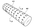
図18Aは、本発明の別の他の実施形態による印刷版の斜視図である。図18Bは図18AのB−B´線に沿った断面図である。 FIG. 18A is a perspective view of a printing plate according to another embodiment of the present invention. 18B is a cross-sectional view taken along the line BB ′ of FIG. 18A.
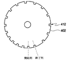
図18A及び図18Bを参照する。本発明の別の他の実施形態による印刷版402は、円筒形状に形成されていることを除いては本発明の一実施形態による印刷版400と実質的に同一である。円筒形印刷版402の外面には印刷溝412アレイが形成されている。印刷溝412アレイは、ローリング方向に向かって間隔が異なって配列されている。すなわち、印刷溝412アレイの開始列における間隔より印刷溝アレイの終了列における間隔がより広く配列されている。ここで印刷溝アレイの開始列とは、実際に転写が開始される列によって定義され、終了列は転写が終了される列によって定義される。
Please refer to FIG. 18A and FIG. 18B. A
このような印刷版402は、スペーサアレイの形成に適用できる。図19は、本発明の別の他の実施形態による印刷版が適用されたスペーサ形成方法の一工程段階の断面図である。
Such a
図19を参照すれば、インク供給装置51から円筒形印刷版402にスペーサを含むインク300が供給されると、印刷版402が回転しながらブレード24によってインク300が印刷溝412に充填され、回転し続けながらこれに接する転写ローラ21の転写シート22に転写される。転写シート22に転写されたインクパターン310は、転写ローラ21のローリング方向に相対的に移動する第2の表示板200上に再転写される。すなわち、インク充填、転写及び再転写が同時に連続的に実行される。以後、硬化、乾燥などの工程を経てスペーサアレイが形成される。
Referring to FIG. 19, when the
図20は、本発明の別の他の実施形態による印刷版の断面図である。 FIG. 20 is a cross-sectional view of a printing plate according to another embodiment of the present invention.
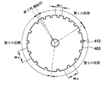
図20を参照する。本実施形態による印刷版403は外面に形成された印刷溝413アレイが等間隔区間を備えることを除いては図18Bの実施形態による印刷版402と同一である。図20を参照すれば、本実施形態では、三つの等間隔区間が設けられている。印刷溝413アレイの終了列に隣接する第3の区間の印刷溝アレイ間隔(w33)は、開始列に隣接する第1の区間の間隔(w31)に比べて広い。また、その間に設けられる第2の区間の印刷溝アレイ間隔(w32)は、第1の区間の間隔(w31)より広く、第3の区間の間隔(w33)より狭い。すなわち、本実施形態による印刷版403においては、等間隔区間が存在するが、全体的に印刷溝413アレイの開始列から終了列に向かうほど間隔が広くなるように配列されている。本実施形態印刷版403においては、等間隔区間が存在するが、各区間の幅が印刷溝413アレイの全体幅に比べて狭いので、等間隔区間による再転写パターンの間隔誤差が大きくならない。従って、例えば表示パネルの遮光領域のうち薄膜トランジスタ以外の位置から外れないようにスペーサアレイを形成することができる。
Refer to FIG. The
以上の実施形態による液晶表示装置の製造方法においては、スペーサが第2の表示板に形成される場合が例示されたが、これに限定されるわけではなく、スペーサは第1の表示板に形成されるようにしてもよい。この場合、スペーサは第1の表示板の遮光領域に形成され、好ましくは、薄膜トランジスタが形成されない遮光領域に形成される。また、以上の実施形態で説明された第1の表示板及び第2の表示板の構造及び製造方法は、多様に変形することがでる。例えば、第1の基板が一つのマスクを用いて半導体層及びデータ線をパターニングする方法及びそれによる構造にも適用することができる。以上のような本発明の多様な適用例又は実施形態は、当業者の立場で容易に理解又は類推することができ、本発明の範囲が曖昧に又は限定的に解釈されることを回避するために具体的な説明を省略する。 In the manufacturing method of the liquid crystal display device according to the above embodiment, the case where the spacer is formed on the second display plate is exemplified. However, the present invention is not limited to this, and the spacer is formed on the first display plate. You may be made to do. In this case, the spacer is formed in the light shielding region of the first display panel, and is preferably formed in the light shielding region where the thin film transistor is not formed. In addition, the structures and manufacturing methods of the first display panel and the second display panel described in the above embodiments can be variously modified. For example, the present invention can be applied to a method of patterning a semiconductor layer and a data line using a single mask on a first substrate and a structure thereof. Various application examples or embodiments of the present invention as described above can be easily understood or inferred from the viewpoint of those skilled in the art, and the scope of the present invention is avoided from being ambiguously or limitedly interpreted. Detailed description will be omitted.
以上、添付した図面を参照して本発明の好適な実施形態を説明したが、当業者であれば、本発明の技術的思想や必須な特徴を変更せずに、本発明が他の具体的な形態で実施され得ることを理解することができる。したがって、上述した好適な実施形態は、例示的なものであり、限定的なものではないと理解される。 The preferred embodiments of the present invention have been described above with reference to the accompanying drawings. However, those skilled in the art will recognize that the present invention is not limited to other specific embodiments without changing the technical idea and essential features of the present invention. It can be understood that it can be implemented in various forms. Accordingly, the preferred embodiments described above are to be understood as illustrative and not restrictive.
本発明は、精密な配線パターンや表示装置のスペーサパターンを形成することに適用され得る。 The present invention can be applied to forming a precise wiring pattern or a spacer pattern of a display device.
10:下部フレーム
20:上部フレーム
21:転写ローラ
22:転写シート
24:ブレード
50:ロールプリント装置
100:第1の表示板
200:第2の表示板
300:インク
350:スペーサ
400:印刷版
410:印刷溝
10: Lower frame 20: Upper frame 21: Transfer roller 22: Transfer sheet 24: Blade 50: Roll printing device 100: First display board 200: Second display board 300: Ink 350: Spacer 400: Printing plate 410: Printing groove
Claims (20)
前記印刷溝に充填されたインクを前記表示パネルの一方の基板に転写する転写シートを備える転写ローラとを含むことを特徴とするロールプリント装置。 The first and second substrates are arranged at equal intervals along the first direction, the intervals are wider in the end row than the start row in the second direction perpendicular to the first direction, and two opposing substrates are arranged. A printing plate comprising a plurality of printing groove arrays having substantially the same cell gap and depth of a display panel comprising:
A roll printing apparatus comprising: a transfer roller including a transfer sheet that transfers the ink filled in the printing groove to one substrate of the display panel.
前記印刷溝は、第1の方向に沿って等間隔に配列されており、前記第1の方向と垂直な第2の方向に沿って開始列より終了列において間隔が広く配列されていることを特徴とする印刷版。 A printing plate comprising a plurality of print groove arrays having substantially the same cell gap and depth of a display panel including two opposing substrates,
The printing grooves are arranged at equal intervals along the first direction, and the intervals are wider at the end row than at the start row along the second direction perpendicular to the first direction. Printing plate featuring.
前記テスト印刷版上に転写シートを備える転写ローラをローリングすることによって前記インクを前記転写シートに転写し、
前記転写シートに転写されたインクをテスト基板上に再転写し、
前記再転写されたインクパターンの間隔と前記スペーサアレイの間隔とを比較することによって、印刷溝アレイの間隔を決定することを含むことを特徴とする印刷版の製造方法。 Filling the groove array of the test printing plate with the same spacing as the spacer array of the display panel including two opposing substrates,
Transferring the ink to the transfer sheet by rolling a transfer roller comprising a transfer sheet on the test printing plate;
Retransfer the ink transferred to the transfer sheet onto the test substrate;
A method for producing a printing plate, comprising: determining a spacing of a printing groove array by comparing a spacing of the re-transferred ink pattern with a spacing of the spacer array.
前記印刷版上に転写シートを備える転写ローラをローリングすることによって前記インクを前記転写シートに転写し、
前記転写シートに転写されたインクを前記表示パネルの一方の基板上に再転写することを含むことを特徴とする表示装置の製造方法。 The first and second substrates are arranged at equal intervals along the first direction, the intervals are wider at the end points than the start points in the second direction perpendicular to the first direction, and two opposing substrates are arranged. Filling the printing groove array of the printing plate having substantially the same cell gap and depth of the display panel including the ink containing the spacer;
Transferring the ink to the transfer sheet by rolling a transfer roller comprising a transfer sheet on the printing plate;
A method of manufacturing a display device, comprising: retransferring the ink transferred to the transfer sheet onto one substrate of the display panel.
One substrate of the display panel includes a plurality of pixels arranged in a matrix, and an interval of ink retransferred in the rolling direction is the same as an interval in the other direction of the adjacent pixels. A method for manufacturing a display device according to claim 19.
Applications Claiming Priority (1)
| Application Number | Priority Date | Filing Date | Title |
|---|---|---|---|
| KR1020050121845A KR20070062106A (en) | 2005-12-12 | 2005-12-12 | Printing plate, method for fabricating the same and roll printing apparatus and method for fabricating display device using the the same |
Publications (2)
| Publication Number | Publication Date |
|---|---|
| JP2007160921A true JP2007160921A (en) | 2007-06-28 |
| JP2007160921A5 JP2007160921A5 (en) | 2009-09-10 |
Family
ID=38137997
Family Applications (1)
| Application Number | Title | Priority Date | Filing Date |
|---|---|---|---|
| JP2006201254A Withdrawn JP2007160921A (en) | 2005-12-12 | 2006-07-24 | Printing plate, its manufacturing method, roll printing device including printing plate, and manufacturing method for display device using roll printing device |
Country Status (3)
| Country | Link |
|---|---|
| US (1) | US20070131124A1 (en) |
| JP (1) | JP2007160921A (en) |
| KR (1) | KR20070062106A (en) |
Cited By (2)
| Publication number | Priority date | Publication date | Assignee | Title |
|---|---|---|---|---|
| JP2010111871A (en) * | 2008-11-07 | 2010-05-20 | Lg Display Co Ltd | Ink composition and method of fabricating liquid crystal display device using the same |
| US9169409B2 (en) | 2008-11-07 | 2015-10-27 | Lg Display Co., Ltd. | Ink composition for imprint lithography and roll printing |
Families Citing this family (3)
| Publication number | Priority date | Publication date | Assignee | Title |
|---|---|---|---|---|
| KR101138428B1 (en) * | 2005-09-06 | 2012-04-26 | 삼성전자주식회사 | Printing apparatus of ink pattern, method for fabricating ink pattern and liquid crystal display using the same |
| KR101019951B1 (en) * | 2008-07-21 | 2011-03-09 | (주)넥셈 | Paste Wheel |
| KR101697276B1 (en) * | 2016-06-02 | 2017-01-17 | 정재용 | Method for laminating a lamination by the arrangement separate structure |
Citations (3)
| Publication number | Priority date | Publication date | Assignee | Title |
|---|---|---|---|---|
| JPH06340054A (en) * | 1993-06-01 | 1994-12-13 | Tokyo Process Service Kk | Screen printing method |
| JP2000094631A (en) * | 1998-09-22 | 2000-04-04 | Canon Inc | Method for offset printing and image display device using it |
| JP2002029032A (en) * | 2000-07-14 | 2002-01-29 | Dainippon Screen Mfg Co Ltd | Printer having platemaking mechanism |
Family Cites Families (11)
| Publication number | Priority date | Publication date | Assignee | Title |
|---|---|---|---|---|
| US5678483A (en) * | 1994-02-16 | 1997-10-21 | Corning Incorporated | Method for printing a black border for a color filter |
| US5813336A (en) * | 1995-12-22 | 1998-09-29 | Heidelberger Druckmaschinen Ag | Printing unit with axially removable printing sleeves |
| KR100798314B1 (en) * | 2001-12-28 | 2008-01-28 | 엘지.필립스 엘시디 주식회사 | An ink printing apparatus for compensating mis-alignment of patterns caused by variation of a substrate and a patterning method using thereof |
| US20030232126A1 (en) * | 2002-06-14 | 2003-12-18 | Yang Michael W. | Method for dispersing spacer on the substrate of a liquid crystal display element and apparatus for dispersion therewith |
| JP4789400B2 (en) * | 2003-02-24 | 2011-10-12 | 株式会社村田製作所 | Method for manufacturing ceramic electronic component and gravure printing method |
| KR100805047B1 (en) * | 2003-09-08 | 2008-02-20 | 엘지.필립스 엘시디 주식회사 | Printing equipment and the patterning method |
| EP1580015A1 (en) * | 2004-03-24 | 2005-09-28 | Kba-Giori S.A. | Process and apparatus for providing identity marks on security documents |
| KR100606441B1 (en) * | 2004-04-30 | 2006-08-01 | 엘지.필립스 엘시디 주식회사 | Method for fabricating cliche and method for forming pattern using the same |
| KR101160833B1 (en) * | 2005-07-11 | 2012-06-28 | 삼성전자주식회사 | Manufacturing apparatus of liquid crystal display |
| KR20080076371A (en) * | 2007-02-15 | 2008-08-20 | 삼성전자주식회사 | Printing plate, spacer printing apparatus having the plate and method for printing spacer using the apparatus |
| US20090145314A1 (en) * | 2007-12-07 | 2009-06-11 | Chemque, Inc. | Intaglio Printing Methods, Apparatuses, and Printed or Coated Materials Made Therewith |
-
2005
- 2005-12-12 KR KR1020050121845A patent/KR20070062106A/en not_active Application Discontinuation
-
2006
- 2006-07-24 JP JP2006201254A patent/JP2007160921A/en not_active Withdrawn
- 2006-11-01 US US11/591,047 patent/US20070131124A1/en not_active Abandoned
Patent Citations (3)
| Publication number | Priority date | Publication date | Assignee | Title |
|---|---|---|---|---|
| JPH06340054A (en) * | 1993-06-01 | 1994-12-13 | Tokyo Process Service Kk | Screen printing method |
| JP2000094631A (en) * | 1998-09-22 | 2000-04-04 | Canon Inc | Method for offset printing and image display device using it |
| JP2002029032A (en) * | 2000-07-14 | 2002-01-29 | Dainippon Screen Mfg Co Ltd | Printer having platemaking mechanism |
Cited By (2)
| Publication number | Priority date | Publication date | Assignee | Title |
|---|---|---|---|---|
| JP2010111871A (en) * | 2008-11-07 | 2010-05-20 | Lg Display Co Ltd | Ink composition and method of fabricating liquid crystal display device using the same |
| US9169409B2 (en) | 2008-11-07 | 2015-10-27 | Lg Display Co., Ltd. | Ink composition for imprint lithography and roll printing |
Also Published As
| Publication number | Publication date |
|---|---|
| KR20070062106A (en) | 2007-06-15 |
| US20070131124A1 (en) | 2007-06-14 |
Similar Documents
| Publication | Publication Date | Title |
|---|---|---|
| CN105629591B (en) | A kind of array substrate, preparation method and liquid crystal display panel | |
| JP4084290B2 (en) | Manufacturing method of liquid crystal display element | |
| US20090066861A1 (en) | Display and Method of Manufacturing the Same | |
| KR20090079159A (en) | Liquid crystal display and method of manufacturing the same | |
| US7487722B2 (en) | Method of manufacturing a display panel with ink recovery | |
| KR20060001425A (en) | Liquid crystal display device and the fabrication method thereof | |
| JP2015148722A (en) | Array substrate and manufacturing method thereof | |
| JP2007160921A (en) | Printing plate, its manufacturing method, roll printing device including printing plate, and manufacturing method for display device using roll printing device | |
| JP2007013084A (en) | Liquid crystal display and its manufacturing method | |
| JP2007025667A (en) | Fabricating apparatus for liquid crystal display device | |
| CN111158182B (en) | Display panel and manufacturing method thereof | |
| JP4516518B2 (en) | Liquid crystal display device using thin film transistor and manufacturing method thereof | |
| US7140296B2 (en) | Method for forming pattern of liquid crystal display device | |
| US20100020258A1 (en) | Thin film transistor substrate, method of manufacturing thereof and liquid crystal display device | |
| WO2018219345A1 (en) | Array substrate, display panel and display device | |
| KR101201707B1 (en) | Liquid crystal display device and method of fabricating the same | |
| US20170082885A1 (en) | Liquid-crystal display device and method of fabricating the same | |
| JP3942590B2 (en) | Manufacturing method of color filter substrate | |
| CN102909983B (en) | Method of fabricating cliche | |
| KR101885925B1 (en) | Array substrate and liquid crystal display device comprising the same | |
| US20090159888A1 (en) | Display panel and method for manufacturing the same | |
| KR101205767B1 (en) | Method of fabricating the array substrate for liquid crystal display device using liquid type organic semiconductor material | |
| KR20070007565A (en) | Manufacturing apparatus of liquid crystal display | |
| US20070117047A1 (en) | Printing plate, method of manufacturing of printing plate and liquid crystal display device using the same | |
| JP2008065012A (en) | Liquid crystal display panel |
Legal Events
| Date | Code | Title | Description |
|---|---|---|---|
| A521 | Request for written amendment filed |
Free format text: JAPANESE INTERMEDIATE CODE: A523 Effective date: 20090723 |
|
| A621 | Written request for application examination |
Free format text: JAPANESE INTERMEDIATE CODE: A621 Effective date: 20090723 |
|
| A521 | Request for written amendment filed |
Free format text: JAPANESE INTERMEDIATE CODE: A523 Effective date: 20100708 |
|
| A131 | Notification of reasons for refusal |
Free format text: JAPANESE INTERMEDIATE CODE: A131 Effective date: 20110906 |
|
| A761 | Written withdrawal of application |
Free format text: JAPANESE INTERMEDIATE CODE: A761 Effective date: 20111007 |