KR20070062106A - Printing plate, method for fabricating the same and roll printing apparatus and method for fabricating display device using the the same - Google Patents
Printing plate, method for fabricating the same and roll printing apparatus and method for fabricating display device using the the same Download PDFInfo
- Publication number
- KR20070062106A KR20070062106A KR1020050121845A KR20050121845A KR20070062106A KR 20070062106 A KR20070062106 A KR 20070062106A KR 1020050121845 A KR1020050121845 A KR 1020050121845A KR 20050121845 A KR20050121845 A KR 20050121845A KR 20070062106 A KR20070062106 A KR 20070062106A
- Authority
- KR
- South Korea
- Prior art keywords
- ink
- display panel
- printing
- printing plate
- groove
- Prior art date
Links
Images


Classifications
-
- G—PHYSICS
- G02—OPTICS
- G02F—OPTICAL DEVICES OR ARRANGEMENTS FOR THE CONTROL OF LIGHT BY MODIFICATION OF THE OPTICAL PROPERTIES OF THE MEDIA OF THE ELEMENTS INVOLVED THEREIN; NON-LINEAR OPTICS; FREQUENCY-CHANGING OF LIGHT; OPTICAL LOGIC ELEMENTS; OPTICAL ANALOGUE/DIGITAL CONVERTERS
- G02F1/00—Devices or arrangements for the control of the intensity, colour, phase, polarisation or direction of light arriving from an independent light source, e.g. switching, gating or modulating; Non-linear optics
- G02F1/01—Devices or arrangements for the control of the intensity, colour, phase, polarisation or direction of light arriving from an independent light source, e.g. switching, gating or modulating; Non-linear optics for the control of the intensity, phase, polarisation or colour
- G02F1/13—Devices or arrangements for the control of the intensity, colour, phase, polarisation or direction of light arriving from an independent light source, e.g. switching, gating or modulating; Non-linear optics for the control of the intensity, phase, polarisation or colour based on liquid crystals, e.g. single liquid crystal display cells
- G02F1/133—Constructional arrangements; Operation of liquid crystal cells; Circuit arrangements
- G02F1/1333—Constructional arrangements; Manufacturing methods
- G02F1/1339—Gaskets; Spacers; Sealing of cells
-
- B—PERFORMING OPERATIONS; TRANSPORTING
- B41—PRINTING; LINING MACHINES; TYPEWRITERS; STAMPS
- B41M—PRINTING, DUPLICATING, MARKING, OR COPYING PROCESSES; COLOUR PRINTING
- B41M1/00—Inking and printing with a printer's forme
Abstract
Description
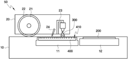
도 1은 본 발명의 일 실시예에 따른 롤 프린트 장치의 개략적인 단면도이다. 1 is a schematic cross-sectional view of a roll printing apparatus according to an embodiment of the present invention.
도 2는 본 발명의 일 실시예에 따른 방법으로 제조된 액정 표시 장치의 단면도이다. 2 is a cross-sectional view of a liquid crystal display manufactured by a method according to an embodiment of the present invention.
도 3은 도 2의 A 부분의 확대도이다.3 is an enlarged view of a portion A of FIG. 2.
도 4 내지 도 6은 본 발명의 일 실시예에 따른 액정 표시 장치의 액정 표시 패널 제조 방법의 공정 단계별 단면도들이다.4 to 6 are cross-sectional views of process steps of a method of manufacturing a liquid crystal display panel of a liquid crystal display according to an exemplary embodiment of the present invention.
도 7은 본 발명의 일 실시예에 따른 액정 표시 장치의 스페이서 형성 방법의 공정 흐름도이다. 7 is a flowchart illustrating a method of forming a spacer of a liquid crystal display according to an exemplary embodiment of the present invention.
도 8a는 본 발명의 일 실시예에 따른 인쇄판의 평면도이다.8A is a plan view of a printing plate according to an embodiment of the present invention.
도 8b는 도 8a의 B - B'선을 따라 자른 단면도이다. FIG. 8B is a cross-sectional view taken along the line BB ′ of FIG. 8A.
도 9 내지 도 12는 본 발명의 일 실시예에 따른 액정 표시 장치의 스페이서 형성 방법의 공정 단계별 단면도들이다.9 to 12 are cross-sectional views illustrating process steps of a method of forming a spacer of a liquid crystal display according to an exemplary embodiment of the present invention.
도 13은 본 발명의 일 실시예에 따른 인쇄판의 제조 방법의 공정 흐름도이 다. 13 is a process flowchart of a method of manufacturing a printing plate according to an embodiment of the present invention.
도 14a 및 도 15a는 본 발명의 일 실시예에 따른 인쇄판의 제조 방법의 공정 단계별 평면도들이다. 14A and 15A are plan views of process steps of a method of manufacturing a printing plate according to an embodiment of the present invention.
도 14b 및 도 15b는 각각 도 14a 및 도 15a의 B - B'선을 따라 자른 단면도들이다. 14B and 15B are cross-sectional views taken along the line BB ′ of FIGS. 14A and 15A, respectively.
도 16은 본 발명의 일 실시예에 따른 방법으로 제조된 인쇄판의 평면도이다.16 is a plan view of a printing plate manufactured by a method according to an embodiment of the present invention.
도 17은 본 발명의 다른 실시예에 따른 인쇄판의 평면도이다.17 is a plan view of a printing plate according to another embodiment of the present invention.
도 18a는 본 발명의 또 다른 실시예에 따른 인쇄판의 사시도이다. 18A is a perspective view of a printing plate according to another embodiment of the present invention.
도 18b는 도 18a의 B - B'선을 따라 자른 단면도이다.FIG. 18B is a cross-sectional view taken along the line BB ′ of FIG. 18A.
도 19는 본 발명의 또 다른 실시예에 따른 인쇄판이 적용된 스페이서 형성 방법의 일 공정 단계의 단면도이다.19 is a cross-sectional view of one process step of a spacer forming method to which a printing plate is applied according to another embodiment of the present invention.
도 20은 본 발명의 또 다른 실시예에 따른 인쇄판의 단면도이다.20 is a cross-sectional view of a printing plate according to another embodiment of the present invention.
<도면의 주요부분에 대한 부호의 설명><Description of the symbols for the main parts of the drawings>
10: 하부 프레임 20: 상부 프레임10: lower frame 20: upper frame
21: 전사 롤러 22: 전사 시트21: transfer roller 22: transfer sheet
24: 블레이드 50: 롤 프린트 장치24: blade 50: roll printing device
100: 제1 표시판 200: 제2 표시판100: first display panel 200: second display panel
300: 잉크 350: 스페이서300: ink 350: spacer
400: 인쇄판 410: 인쇄홈400: printing plate 410: printing groove
본 발명은 롤 프린트 장치에 관한 것으로서, 보다 상세하게는 블레이드를 이용한 롤 프린트 장치, 이를 이용한 잉크 패턴 형성 방법 및 액정 표시 장치의 제조 방법에 관한 것이다.The present invention relates to a roll printing apparatus, and more particularly, to a roll printing apparatus using a blade, an ink pattern forming method using the same, and a manufacturing method of a liquid crystal display.
정보화 사회가 발전함에 따라 표시 장치에 대한 요구도 다양한 형태로 변화하고 있다. 종래 텔레비전이나 컴퓨터 모니터 등의 표시 장치에 많이 사용되었던 음극선관(Cathode Ray Tube; CRT)을 대신하여 대형화, 평면화, 슬림화 등의 요구에 부합되는 액정 표시 장치(Liquid Crystal Display), 유기 EL 표시 장치(Electro Luminescent Display), 전계 방출 표시 장치(Field Emission Display; FED), 플라즈마 표시 패널(Plasma Display Panel; PDP) 등의 다양한 평판 표시 장치(Flat Panel Display)가 개발되어 활용되고 있다.As the information society develops, the demand for display devices is also changing in various forms. Instead of Cathode Ray Tube (CRT), which has been widely used in displays such as televisions and computer monitors, liquid crystal displays and organic EL displays that meet the needs of large size, planarization, and slimming, etc. Various flat panel displays such as an electro luminescent display, a field emission display (FED), and a plasma display panel (PDP) have been developed and utilized.
평판 표시 장치는 서로 다른 기능을 하며, 대향 배치된 제1 및 제2 표시판을 포함한다. 제1 및 제2 표시판은 소정 간격 이격되어 배치되며, 제1 표시판과 제2 표시판의 사이에는 상기 간격을 일정하게 유지시켜 주는 스페이서가 구비된다.The flat panel display device has different functions and includes first and second display panels disposed to face each other. The first and second display panels are spaced apart from each other by a predetermined interval, and a spacer is provided between the first display panel and the second display panel to keep the gap constant.
상기 스페이서로는 비드 스페이서와 컬럼 스페이서가 사용된다. 비드 스페이서는 주로 산포법으로 형성한다. 산포법은 공정이 단순하고 제조 비용이 저렴하지만, 스페이서의 산포 위치를 정밀하게 제어하기 어려워, 화소 영역에 산포될 경우 화질을 저하시키게 된다.Bead spacers and column spacers are used as the spacers. Bead spacers are mainly formed by a scattering method. Although the scattering method is simple and inexpensive to manufacture, it is difficult to precisely control the scattering position of the spacer, and thus the image quality is degraded when scattered in the pixel region.
컬럼 스페이서는 주로 유기물을 사진 식각 공정에 의해 패터닝하여 형성하기 때문에 위치 제어에 유리하지만, 공정이 복잡해지고, 공정 시간 및 제조 비용이 증가하게 된다.Column spacers are advantageous for position control because they are mainly formed by patterning organic materials by a photolithography process, but the process is complicated, and process time and manufacturing cost are increased.
최근에는, 상기한 바와 같은 산포법 및 사진 식각법에 대한 대체하는 스페이서 형성 방법으로서, 롤 프린트 장치를 이용한 인쇄법이 연구되고 있다. 롤 프린트 장치를 이용한 인쇄법은 제조 공정이 단순하고, 제조 시간을 단축할 수 있으며, 제조 비용이 저렴하다. Recently, a printing method using a roll printing apparatus has been studied as an alternative spacer forming method for the above-described dispersion method and photolithography method. The printing method using a roll printing apparatus has a simple manufacturing process, can shorten manufacturing time, and is low in manufacturing cost.
상기 인쇄법은 산포법에 비해 비교적 정확한 위치에 스페이서 어레이를 형성할 수 있지만, 전사 시트의 특성에 따라 전사 오차가 발생할 수 있다. 이러한 오차는 기판이 대형화되면서 롤 프린트 장치에 구비된 전사 롤러의 롤링 거리가 길어짐에 따라 더욱 커지게 된다. 스페이서가 상기 오차에 따라 정확한 위치에 형성되지 못할 경우, 셀갭 유지에 효과적이지 못하며, 오차가 누적되어 화소 영역에 형성될 경우 개구율을 감소시키는 등 화질을 저하시키게 된다. The printing method may form a spacer array at a relatively accurate position compared to the scattering method, but a transfer error may occur depending on the characteristics of the transfer sheet. This error becomes larger as the substrate becomes larger and the rolling distance of the transfer roller provided in the roll printing apparatus becomes longer. If the spacer is not formed at the correct position according to the error, the spacer is not effective in maintaining the cell gap, and when the error is accumulated and formed in the pixel area, the image quality is reduced, such as decreasing the aperture ratio.
본 발명이 이루고자 하는 기술적 과제는 대형 기판 상에도 정밀한 잉크 패턴 형성이 가능한 롤 프린트 장치를 제공하고자 하는 것이다.It is an object of the present invention to provide a roll printing apparatus capable of forming a precise ink pattern even on a large substrate.
본 발명이 이루고자 하는 다른 기술적 과제는 상기한 바와 같은 롤 프린트 장치에 사용되는 인쇄판을 제공하고자 하는 것이다.Another technical problem to be achieved by the present invention is to provide a printing plate used in the roll printing apparatus as described above.
본 발명이 이루고자 하는 또 다른 기술적 과제는 상기한 바와 같은 인쇄판의 제조 방법을 제공하고자 하는 것이다.Another technical problem to be achieved by the present invention is to provide a method for manufacturing a printing plate as described above.
본 발명이 이루고자 하는 또 다른 기술적 과제는 상기한 바와 같은 롤 프린 트 장치를 이용한 표시 장치의 제조 방법을 제공하고자 하는 것이다.Another object of the present invention is to provide a method of manufacturing a display device using the roll printing device as described above.
본 발명의 기술적 과제들은 이상에서 언급한 기술적 과제로 제한되지 않으며, 언급되지 않은 또 다른 기술적 과제들은 아래의 기재로부터 당업자에게 명확하게 이해될 수 있을 것이다.Technical problems of the present invention are not limited to the technical problems mentioned above, and other technical problems not mentioned will be clearly understood by those skilled in the art from the following description.
상기 기술적 과제를 달성하기 위한 본 발명의 일 실시예에 따른 롤 프린트 장치는 제1 방향을 따라 등간격으로 배열되어 있고, 상기 제1 방향과 수직한 제2 방향의 시작열보다 끝열에서 간격이 크게 배열되어 있으며, 깊이가 표시 패널의 셀갭과 실질적으로 동일한 다수개의 인쇄홈 어레이를 포함하는 인쇄판 및 상기 인쇄홈에 충진된 잉크를 전사하는 전사 시트를 구비하는 전사 롤러를 포함한다.Roll printing apparatus according to an embodiment of the present invention for achieving the above technical problem is arranged at equal intervals along the first direction, the interval larger in the end row than the start column in the second direction perpendicular to the first direction And a transfer plate having a printing plate arranged and having a depth of substantially the same as the cell gap of the display panel, the printing plate comprising a plurality of printing groove arrays, and a transfer sheet transferring the ink filled in the printing grooves.
상기 다른 기술적 과제를 달성하기 위한 본 발명의 일 실시예에 따른 인쇄판은 깊이가 표시 장치의 셀갭과 실질적으로 동일한 다수개의 인쇄홈 어레이를 구비하는 인쇄판으로서, 상기 인쇄홈은 제1 방향을 따라 등간격으로 배열되어 있고, 상기 제1 방향과 수직한 제2 방향을 따라 시작열보다 끝열에서 간격이 크게 배열되어 있다.The printing plate according to an embodiment of the present invention for achieving the another technical problem is a printing plate having a plurality of print groove array depth is substantially the same as the cell gap of the display device, the printing groove is equally spaced along the first direction The gaps are arranged in the end row more than the start row along the second direction perpendicular to the first direction.
상기 또 다른 기술적 과제를 달성하기 위한 본 발명의 일 실시예에 따른인쇄판의 제조 방법은 스페이서 어레이와 동일한 간격을 갖는 오목홈 어레이를 구비하는 테스트 인쇄판 상에 잉크를 충진하는 단계와, 상기 테스트 인쇄판 위에 전사 시트를 구비하는 전사 롤러를 롤링하여 상기 잉크를 상기 전사 시트에 전사하는 단계와, 상기 전사 시트에 전사된 잉크를 테스트 기판 상에 재전사하는 단계와, 상기 재전사된 잉크 패턴의 간격과 상기 스페이서 어레이의 간격을 비교하여 인쇄홈 어레이의 간격을 결정하는 단계를 포함한다.According to another aspect of the present invention, there is provided a method of manufacturing a printing plate, comprising: filling ink on a test printing plate having a concave groove array having the same spacing as a spacer array; Rolling the transfer roller including a transfer sheet to transfer the ink to the transfer sheet, retransferring the ink transferred to the transfer sheet onto a test substrate, and spacing between the retransmitted ink patterns and the Comparing the spacing of the spacer arrays to determine the spacing of the print groove arrays.
상기 또 다른 기술적 과제를 달성하기 위한 본 발명의 일 실시예에 따른 표시 장치의 제조 방법은 제1 방향을 따라 등간격으로 배열되어 있고, 상기 제1 방향과 수직한 제2 방향의 시작점보다 끝점에서 간격이 크게 배열되어 있으며, 깊이가 표시 패널의 셀갭과 실질적으로 동일한 인쇄판의 인쇄홈 어레이에 스페이서를 포함하는 잉크를 충진하는 단계와, 상기 인쇄판 위에 전사 시트를 구비하는 전사 롤러를 롤링하여 상기 잉크를 상기 전사 시트에 전사하는 단계 및 상기 전사 시트에 전사된 잉크를 표시판 상에 재전사하는 단계를 포함한다.According to another aspect of the present invention, there is provided a method of manufacturing a display device, which is arranged at equal intervals in a first direction and is disposed at an end point from a start point of a second direction perpendicular to the first direction. Filling the ink including a spacer into a printing groove array of a printing plate having a large spacing and having a depth substantially equal to a cell gap of the display panel; and rolling the transfer roller including a transfer sheet on the printing plate to roll the ink. Transferring the transferred sheet to the transfer sheet and re-transferring the transferred ink onto the transfer sheet.
기타 실시예들의 구체적인 사항들은 상세한 설명 및 도면들에 포함되어 있다.Specific details of other embodiments are included in the detailed description and the drawings.
본 발명의 이점 및 특징, 그리고 그것들을 달성하는 방법은 첨부되는 도면과 함께 상세하게 후술되어 있는 실시예들을 참조하면 명확해질 것이다. 그러나 본 발명은 이하에서 개시되는 실시예들에 한정되는 것이 아니라 서로 다른 다양한 형태로 구현될 것이며, 단지 본 실시예들은 본 발명의 개시가 완전하도록 하며, 본 발명이 속하는 기술분야에서 통상의 지식을 가진 자에게 발명의 범주를 완전하게 알려주기 위해 제공되는 것이며, 본 발명은 청구항의 범주에 의해 정의될 뿐이다. 도면에서 층 및 영역들의 크기 및 상대적인 크기는 설명의 명료성을 위해 과장된 것일 수 있다. Advantages and features of the present invention and methods for achieving them will be apparent with reference to the embodiments described below in detail with the accompanying drawings. However, the present invention is not limited to the embodiments disclosed below, but will be implemented in various forms, and only the present embodiments are intended to complete the disclosure of the present invention, and the general knowledge in the art to which the present invention pertains. It is provided to fully convey the scope of the invention to those skilled in the art, and the present invention is defined only by the scope of the claims. In the drawings, the sizes and relative sizes of layers and regions may be exaggerated for clarity.
소자(elements) 또는 층이 다른 소자 또는 층의 "위(on)" 또는 "상(on)"으로 지칭되는 것은 다른 소자 또는 층의 바로 위뿐만 아니라 중간에 다른 층 또는 다른 소자를 개재한 경우를 모두 포함한다. 반면, 소자가 "직접 위(directly on)" 또는 "바로 위"로 지칭되는 것은 중간에 다른 소자 또는 층을 개재하지 않은 것을 나타낸다. 명세서 전체에 걸쳐 동일 참조 부호는 동일 구성 요소를 지칭한다. "및/또는"은 언급된 아이템들의 각각 및 하나 이상의 모든 조합을 포함한다. When elements or layers are referred to as "on" or "on" of another element or layer, intervening other elements or layers as well as intervening another layer or element in between. It includes everything. On the other hand, when a device is referred to as "directly on" or "directly on" indicates that no device or layer is intervened in the middle. Like reference numerals refer to like elements throughout. “And / or” includes each and all combinations of one or more of the items mentioned.
이하, 첨부된 도면을 참조하여 본 발명의 일 실시예에 따른 롤 프린트 장치에 대하여 설명한다. Hereinafter, a roll printing apparatus according to an embodiment of the present invention will be described with reference to the accompanying drawings.
도 1은 본 발명의 일 실시예에 따른 롤 프린트 장치의 개략적인 단면도이다. 1 is a schematic cross-sectional view of a roll printing apparatus according to an embodiment of the present invention.
도 1을 참조하면, 롤 프린트 장치(50)는 표시판 상에 다양한 잉크 패턴을 인쇄하는데 사용되는 장치로서, 인쇄판(400)과 인쇄판(400)에 충진된 잉크를 표시판 상으로 전사하는 전사 롤러(21)를 포함한다. 롤 프린트 장치(50)에 의해 인쇄될 수 있는 잉크 패턴의 종류는 다양하지만, 이하에서는 표시 장치의 표시 패널간 셀갭을 유지하기 위한 스페이서 어레이를 형성하는 경우를 예로 들어 설명하기로 한다.Referring to FIG. 1, the
인쇄판(400)은 목적으로 하는 대상 패턴인 스페이서 어레이를 형성하기 위한 다수개의 인쇄홈(410) 어레이를 구비한다. 여기서, 인쇄홈(410) 어레이의 하나의 인쇄홈(410)은 스페이서 어레이의 하나의 스페이서에 대응한다. 하나의 스페이서는 하나의 단위 스페이서로 이루어질 수도 있지만, 그에 제한되지 않으며, 다수개의 단위 스페이서의 집합으로 이루어질 수도 있다. 인쇄홈(410) 어레이에 대한 더욱 상세한 설명은 후술하기로 한다.The
인쇄판(400)은 하부 프레임(10)에 설치되어 있는 인쇄판 지지대(11)에 의해 수납된다. 하부 프레임(10)에는 인쇄판 지지대(11)와 나란하게 기판 지지대(12)가 설치되어 있다. 기판 지지대(12)에는 표시판 등의 대상 기판이 위치하며, 여기에서 잉크 인쇄가 이루어진다.The
인쇄판(400)의 위쪽에는 전사 롤러(21)가 위치한다. 전사 롤러(21)는 예컨대 원통형으로 형성될 수 있으며, 외면을 전사 시트(22)가 덮고 있다. 전사 시트(22)는 잉크(300)와의 부착성이 우수한 재질로 이루어지며, 예컨대 친수성이 우수한 실리콘을 포함할 수 있다. 전사 시트(22)는 인쇄판(400)으로부터의 전사 및 표시판으로의 재전사가 용이하도록 탄성을 가지거나, 경도가 작을 수 있다. The
전사 롤러(21)는 하부 프레임(10)의 위에서 하부 프레임(10)과 상대적으로 왕복 운동하는 상부 프레임(20)에 설치된다. 일예로, 하부 프레임(10)은 고정된 상태에서, 상부 프레임(20)이 하부 프레임(10) 위를 왕복 운동한다. 이때, 전사 롤러(21)가 회전하면서, 전사 롤러(21)를 덮고 있는 전사 시트(22)가 인쇄판(400)의 상면 및/또는 표시판(200)의 상면과 접촉하도록 상부 프레임(20)의 위치를 하부 프레임(10)에 근접하게 조절한다. 한편, 전사 롤러(21)의 전사 시트(22)가 표시판(200)의 상면에 반드시 접촉할 필요는 없지만, 적어도 인쇄판(400)으로부터 전사 시트(22)에 전사된 잉크가 표시판(200)의 상면에 닿을 수 있을 정도의 거리는 유지되어야 한다.The
상부 프레임(20)은 또한, 잉크 공급 장치(23) 및 블레이드(24)를 더 포함할 수 있다. 잉크 공급 장치(23) 및/또는 블레이드(24)는 잉크(300)가 전사되는 경우의 전사 롤러(21)의 롤링 방향에 대하여, 전사 롤러(21)의 앞쪽에 위치할 수 있다. The
블레이드(24)는 잉크 공급 장치(23)의 뒤쪽에 위치하며 인쇄홈(410) 어레이의 폭에 대응하는 넓은 폭을 가진다. 블레이드(24)는 인쇄홈(410) 어레이에 잉크(300)를 충진하고, 인쇄판(400) 상면에 잔류하는 잉크(300)를 제거한다.The
이하, 본 발명의 일 실시예에 따른 롤 프린트 장치 및 그에 포함된 인쇄판을 사용하여 표시 장치를 제조하는 방법에 대하여 설명한다. 이하에서는 상기 제조 방법이 적용되는 표시 장치로서 액정 표시 장치가 예시되지만, 그에 제한되는 것은 아니며, FED, 유기 EL 표시 장치, PDP 장치 등에도 적용될 수 있음은 물론이다. Hereinafter, a method of manufacturing a display device using a roll printing apparatus and a printing plate included therein according to an embodiment of the present invention will be described. Hereinafter, a liquid crystal display device is exemplified as a display device to which the manufacturing method is applied, but the present invention is not limited thereto and may be applied to a FED, an organic EL display device, a PDP device, and the like.
먼저 본 발명의 일 실시예에 따른 방법으로 제조된 액정 표시 장치의 액정 표시 패널에 대해 설명한다. 도 2는 본 발명의 일 실시예에 따른 방법으로 제조된 액정 표시 패널의 단면도이다. First, a liquid crystal display panel of a liquid crystal display device manufactured by a method according to an embodiment of the present invention will be described. 2 is a cross-sectional view of a liquid crystal display panel manufactured by a method according to an embodiment of the present invention.
도 2를 참조하면, 액정 표시 장치의 화상을 표시하는 액정 표시 패널은 제1 표시판(100), 그에 대향하는 제2 표시판(200) 및 제1 표시판(100)과 제2 표시판(200) 사이에 개재된 액정층(미도시)을 포함한다. 제1 표시판(100)과 제2 표시판(200)은 셀갭(G)을 유지하며 평행하게 대향 배치되어 있다. 제1 표시판(100)과 제2 표시판(200) 사이의 액정층에는 셀갭(g) 유지를 위한 스페이서(350) 어레이가 배치되어 있다. Referring to FIG. 2, a liquid crystal display panel displaying an image of a liquid crystal display device includes a
도 3은 도 2의 A 부분의 확대도이다. 이하, 도 3을 참조하여 본 발명의 일 실시예에 따른 방법으로 제조된 액정 표시 패널에 대해 더욱 상세히 설명한다.3 is an enlarged view of a portion A of FIG. 2. Hereinafter, a liquid crystal display panel manufactured by the method according to an exemplary embodiment of the present invention will be described in more detail with reference to FIG. 3.
도 3에 도시된 바와 같이 제1 표시판(100)은 투명한 유리, 플라스틱 등으로 이루어진 제1 절연 기판(110) 상에 형성된 다수개의 배선 패턴을 포함한다. 구체적 으로, 제1 절연 기판(110) 위에 알루미늄(Al), 구리(Cu), 은(Ag), 몰리브덴(Mo), 크롬(Cr), 티타늄(Ti), 탄탈륨(Ta) 또는 이들의 합금 등의 도전성 물질로 이루어진 게이트 전극(126)이 형성되어 있다. 게이트 전극(126) 위에는 질화 규소(SiNx) 등으로 이루어진 게이트 절연막(130)이 제1 절연 기판(110)의 전면을 덮고 있다. 게이트 절연막(130) 위에는 수소화 비정질 규소 등의 반도체로 이루어진 반도체층(140)이 형성되어 있다. 반도체층(140)은 적어도 일부가 게이트 전극(126)과 중첩되도록 위치한다. 반도체층(140) 위에는 n형 불순물이 고농도로 도핑된 n+ 수소화 비정질 규소 등으로 이루어진 저항성 접촉층(155, 156)이 형성되어 있다. As shown in FIG. 3, the
저항성 접촉층(155, 156) 위에는 알루미늄(Al), 구리(Cu), 은(Ag), 몰리브덴(Mo), 크롬(Cr), 티타늄(Ti), 탄탈륨(Ta) 또는 이들의 합금 등의 도전성 물질로 이루어진 소스 전극(165)과 드레인 전극(166)이 서로 분리되어 위치한다. On the
상기한 바와 같은 게이트 전극(126), 반도체층(140), 소스 전극(165) 및 드레인 전극(166)은 화소 전극(180)을 스위칭하는 박막 트랜지스터(Thin Film Transistor)를 구성한다. 여기서 게이트 전극(126)은 박막 트랜지스터의 제어단을 이루며, 소스 전극(165)과 드레인 전극(166)은 각각 박막 트랜지스터의 입력단 및 출력단을 이룬다. 반도체층(140)은 박막 트랜지스터의 채널 영역을 형성한다. 한편, 저항성 접촉층(155, 156)은 소스 전극(165) 및 드레인 전극(166)의 분리 형상과 유사하게 분리되도록 형성되어 소스 전극(165) 및 드레인 전극(166)과 하부의 반도체층(140) 사이의 접촉 저항을 줄여주는 역할을 한다.The
소스 전극(165) 및 드레인 전극(166) 위에는 질화 규소, 산화 규소(SiOx) 및 /또는 유기물 등으로 이루어진 보호막(170)이 형성되어 있다. 보호막(170) 위에는 ITO(Indium Tin Oxide), IZO(Indium Zinc Oxide) 등의 투명한 도전성 물질로 이루어진 화소 전극(180)이 형성되어 있다. 화소 전극(180)은 컨택홀(176)을 통하여 박막 트랜지스터의 드레인 전극(166)과 전기적으로 연결되며, 매트릭스 형상으로 배열된다.A
또한 도시하지는 않았지만, 화소 전극(180) 위에는 배향막이 형성될 수 있다. Although not shown, an alignment layer may be formed on the
다음으로 제2 표시판(200)에 대해 설명하면, 투명한 유리, 플라스틱 등으로 이루어진 제2 절연 기판(210) 아래에 크롬(Cr) 등의 불투명 금속 또는 카본 블랙 등을 포함하는 불투명 유기물 등으로 이루어진 차광 패턴(220)이 형성되어 있다. 차광 패턴(220)은 격자 모양으로 형성되어 화소를 정의한다. 화소는 차광 패턴(220)에 의해 정의되어 매트릭스 형상으로 배열된다. 차광 패턴(220) 아래에는 컬러 필터(230)가 형성되어 있다. 컬러 필터(230)는 화소 영역을 채우며, 적색(R), 녹색(G), 청색(B)을 띠는 유기물로 이루어진다. 각각의 색은 일정한 패턴으로 반복적으로 배열되어 있다. 컬러 필터(230) 아래에는 이들의 단차를 완화하는 오버코트막(240)이 위치하며, 오버코트막(240) 아래에는 제1 표시판(100)의 화소 전극(180)과 함께 전계를 형성하는 공통 전극(250)이 형성되어 있다. 공통 전극(250) 아래에는 배향막이 배치될 수 있다.Next, the
제1 표시판(100)과 제2 표시판(200)의 사이에는 스페이서(350)가 위치하여 제1 표시판(100)과 제2 표시판(200)의 셀갭(g1, g2)을 유지한다. The
액정 표시 장치는 백라이트 등으로부터 출사된 빛을 이용하여 화상을 표시하는데, 액정 패널의 빛 투과 여부에 따라 투광 영역 및 차광 영역으로 나뉜다. 차광 영역을 구성하는 구조물로는 제2 표시판(200)의 차광 패턴(220)과 제1 표시판(100)의 박막 트랜지스터 및 그에 연결된 배선을 들 수 있다. 제2 표시판(200)의 컬러 필터(230)와 제1 표시판(100)의 화소 전극(180)이 중첩하는 영역은 투광 영역을 이룬다.The liquid crystal display displays an image using light emitted from a backlight and the like, and is divided into a light transmitting area and a light blocking area according to whether the liquid crystal panel transmits light. The structure of the light blocking region may include a
또 하나의 차광 영역을 구성하는 인자로는 상기한 바와 같은 스페이서(350)를 들 수 있다. 액정 표시 장치에서는 개구율 확보가 중요한데, 스페이서(350)가 투광 영역에 위치하게 되면, 개구율이 감소하게 된다. 또한, 스페이서(350)가 화소 영역에 위치할 경우, 빛샘 현상을 유발할 수도 있다. 따라서 스페이서(350)는 차광 영역에 배치되는 것이 바람직하다. 일예로, 제2 표시판의 차광 패턴(220) 아래에 배치될 수 있다. The factor constituting another light shielding region may be the
한편, 액정 표시 패널의 셀갭은 제1 및 제2 표시판(100, 200)에 구비된 구조물에 의한 단차에 의해 영역별로 다소 차이가 있다. 차광 영역 내에서도 제1 표시판(100)의 박막 트랜지스터가 형성된 영역에서의 셀갭(g1)이 박막 트랜지스터가 형성되지 않은 영역에서의 셀갭(g2)보다 더 좁다. 따라서, 화소별로 동일한 셀갭을 유지하기 위해서는 스페이서(350)가 일정한 영역에 배열될 필요가 있다. 제1 표시판(100) 및 제2 표시판(200)의 압착에 의한 박막 트랜지스터의 충격을 방지하는 관점 에서 스페이서(350)는 차광 영역 중 제2 표시판(200)의 차광 패턴(220)과 제1 표시판(100)의 박막 트랜지스터가 형성되지 않은 영역 사이에 배치되는 것이 바람직하다.On the other hand, the cell gap of the liquid crystal display panel is slightly different for each region due to the step by the structure provided in the first and second display panels (100, 200). Even in the light blocking region, the cell gap g 1 in the region where the thin film transistor of the
스페이서(350)의 형상은 도 3 및 본 명세서의 몇몇 도면들에서 구형으로 모식화되어 도시되어 있지만, 기둥형으로 형성될 수도 있으며, 이에 제한되지 않고, 다양한 형상이 가능하다. 또한, 2 이상의 구형의 단위 스페이서가 모여서 하나의 스페이서를 구성할 수도 있다.Although the shape of the
계속해서, 상기한 바와 같은 액정 표시 장치의 액정 표시 패널을 제조하는 방법에 대해 설명한다. 도 4 내지 도 6은 본 발명의 일 실시예에 따른 액정 표시 장치의 액정 표시 패널 제조 방법의 공정 단계별 단면도들이다. 본 발명의 일 실시예에 따른 액정 표시 패널의 제조 방법은 제1 표시판을 준비하는 단계, 제2 표시판을 준비하는 단계 및 제2 표시판 상에 스페이서 어레이를 형성하는 단계를 포함한다.Subsequently, the method of manufacturing the liquid crystal display panel of the above liquid crystal display device is demonstrated. 4 to 6 are cross-sectional views of process steps of a method of manufacturing a liquid crystal display panel of a liquid crystal display according to an exemplary embodiment of the present invention. A method of manufacturing a liquid crystal display panel according to an exemplary embodiment of the present invention includes preparing a first display panel, preparing a second display panel, and forming a spacer array on the second display panel.
도 2, 도 3 및 도 4를 참조하면, 먼저 제1 표시판(100)을 준비한다. 구체적으로, 유리 등으로 이루어진 제1 절연 기판(110) 상에 알루미늄(Al), 구리(Cu), 은(Ag), 몰리브덴(Mo), 크롬(Cr), 티타늄(Ti), 탄탈륨(Ta) 또는 이들의 합금 등의 도전성 물질을 증착하고 패터닝하여 제1 방향으로 나란하게 연장되어 있는 복수의 게이트선(122) 및 게이트선(122)이 확장되어 이루어지는 게이트 전극(126)을 형성한다. 이어서, 전면에 질화 규소를 증착하여 게이트 절연막(130)을 형성한다. 이어서, 수소화 비정질 규소, n형 불순물이 고농도로 도핑된 n+ 수소화 비정질 규소를 증착한 다음 패터닝하여, 반도체층 및 반도체층과 실질적으로 동일한 패턴을 갖는 저항성 접촉층을 형성한다. 이어서, 도전성 물질을 증착하고 패터닝하여 제2 방향으로 나란하게 연장되어 있는 복수의 데이터선(162), 데이터선(162)에 연결된 소스 전극(165) 및 그와 이격된 드레인 전극(166)을 형성하고, 하부의 저항성 접촉층을 일부 노출시킨다. 이어서, 소스 전극(165) 및 드레인 전극(166)을 식각 마스크로 이용하여 일부 노출된 저항성 접촉층을 패터닝하여 하부의 반도체층을 노출한다. 이어서, 질화 규소 등을 증착하고 패터닝하여 컨택홀(176)을 구비하는 보호막(170)을 형성한다. 이어서, 보호막(170) 상에 ITO 또는 IZO 등을 증착하고 패터닝하여, 드레인 전극(166)과 전기적으로 연결된 화소 전극(180)을 형성한다. 이로써 제1 기판(100)이 제공된다.2, 3, and 4, first, the
이어서, 제2 표시판(200)을 준비한다. 도 5에서는 도 2 및 도 3에 도시된 제2 표시판이 뒤집힌 상태가 도시되어 있다. 이하에서는 도 5에 도시된 상태를 기준으로 방향을 언급할 것이다. 이는 앞서 언급된 방향과 반대일 수 있지만, 동일한 상대적 위치 관계를 나타냄을 용이하게 이해할 수 있을 것이다. Next, the
도 2, 도 3 및 도 5를 참조하면, 구체적으로 제2 절연 기판(210) 상에 크 크롬(Cr) 등의 불투명 금속 또는 카본 블랙 등을 포함하는 불투명 유기물을 증착하고 패터닝하여 차광 패턴(220)을 형성한다. 이때, 제2 절연 기판(210)의 최외곽부의 차광 패턴(221)은 화소 영역의 차광 패턴(220)에 비해 넓은 폭을 갖도록 형성한다. 이어서, 감광성 적색 레지스트를 도포하고, 노광 및 현상하여 적색 컬러 필터를 형성한다. 이어서 동일한 방법으로 녹색 및 청색 컬러 필터를 형성한다. 이로써 적, 녹 청색의 컬러 필터(230)가 형성된다. 이어서, 전면에 유기 물질 및 ITO 또는 IZO 등을 순차적으로 적층하여 오버코트막(240) 및 공통 전극(250)을 형성한다. 이로써 제2 기판(200)이 제공된다.Referring to FIGS. 2, 3, and 5, an opaque organic material including an opaque metal such as chromium (Cr) or carbon black, etc. is deposited and patterned on the second insulating
도 2, 도 3 및 도 6을 참조하면, 이어서 제2 표시판(200)의 차광 패턴 상에 스페이서(350) 어레이를 형성한다. 스페이서(350) 어레이는 바람직하게는 화소의 경계마다 하나씩 형성된다. 즉, 이웃하는 스페이서 간의 일 방향 간격은 이웃하는 일 방향 화소간의 간격과 동일하고, 이웃하는 스페이서 간의 타 방향 간격은 이웃하는 타 방향 화소간의 간격과 동일할 수 있다. 또한 스페이서(350) 어레이는 다수개의 화소마다 하나씩 형성될 수도 있다. 본 단계의 스페이서(350) 어레이 형성 방법에 대해서는 뒤에서 더욱 상세히 설명하기로 한다. 2, 3, and 6, an array of
이어서, 스페이서(350) 어레이가 형성된 제2 표시판(200)에 제1 표시판(100)을 대향 배치하고, 실런트 등을 제1 표시판(100) 및/또는 제2 표시판(200)의 주변부에 도포하여 제1 표시판(100)과 제2 표시판(200)을 결합한다. 이어서, 제1 표시판(100)과 제2 표시판(200) 사이에 액정 분자를 주입하여 액정층을 형성한다. 한편, 액정층의 형성은 제1 표시판(100)과 제2 표시판(200)의 결합 이전에 제1 표시판(100) 또는 제2 표시판(200) 상에 먼저 적하 또는 산포되어 형성될 수도 있다. 이로써 액정 표시 장치의 액정 표시 패널이 완성된다. 이와 같은 액정 표시 패널의 외측면에 편광판을 부착하고, 백라이트를 배치함으로써 액정 표시 장치가 완성된다.Subsequently, the
이하, 도 6에 도시된 바와 같은 배열을 갖는 스페이서 어레이의 형성 방법에 대하여 더욱 상세히 설명한다. 스페이서 어레이 형성 방법에는 본 발명의 일 실시예에 따른 롤 프린트 장치가 사용될 수 있으며, 이하에서 예시될 것이다.Hereinafter, a method of forming a spacer array having the arrangement as shown in FIG. 6 will be described in more detail. A roll printing apparatus according to an embodiment of the present invention may be used for the spacer array forming method, which will be illustrated below.
도 7은 본 발명의 일 실시예에 따른 액정 표시 장치의 스페이서 어레이 형성 방법의 공정 흐름도이다. 도 8a는 본 발명의 일 실시예에 따른 인쇄판의 평면도이다. 도 8b는 도 8a의 B - B'선을 따라 자른 단면도이다. 도 9 내지 도 12는 본 발명의 일 실시예에 따른 액정 표시 장치의 스페이서 형성 방법의 공정 단계별 단면도들이다.7 is a flowchart illustrating a method of forming a spacer array of a liquid crystal display according to an exemplary embodiment of the present invention. 8A is a plan view of a printing plate according to an embodiment of the present invention. FIG. 8B is a cross-sectional view taken along the line BB ′ of FIG. 8A. 9 to 12 are cross-sectional views illustrating process steps of a method of forming a spacer of a liquid crystal display according to an exemplary embodiment of the present invention.
도 7 및 도 8a, 도 8b를 참조하면, 먼저 인쇄판을 준비한다(S1).Referring to FIGS. 7 and 8A and 8B, first, a printing plate is prepared (S 1 ).
인쇄판(400)에는 인쇄홈(410) 어레이가 배열되어 있다. 인쇄홈(410)의 깊이(h)는 스페이서의 높이와 실질적으로 동일하다. 여기서 '실질적으로 동일'하다는 의미는 물리적으로 완전히 동일한 경우뿐만 아니라, 공정에 따른 마진이나 수율에 의해 다소 차이가 나는 경우를 포함한다. 또한, 상술한 바와 같이 액정 표시 패널의 셀갭은 박막 트랜지스터가 위치하는지 여부에 따라 다소 차이가 나지만, 이와 같은 오차는 전체의 셀갭에 비해 미세하기 때문에 무시될 수 있으며, 이 경우 각 영역에서의 셀갭은 '실질적으로 동일'한 것으로 언급될 수 있다. 상기의 관점에서 스페이서의 높이는 액정 표시 패널의 셀갭과 실질적으로 동일하며, 인쇄홈의 깊이는 액정 표시 패널의 셀갭과 실질적으로 동일하다.In the
한편, 후속 공정인 롤링 공정에서 전사 롤러의 롤링 방향이 도 8a의 오른쪽 행 방향(x)일 때, 롤링에 의한 전사가 처음 시작되는 인쇄홈 어레이의 왼쪽 열을 ' 시작열'이라고 정의하고, 전사가 끝나는 인쇄홈 어레이의 오른쪽 열을 '끝열'로 정의하기로 하면, 인쇄홈(410) 어레이는 열 방향(y)으로는 동일한 간격(d1)을 갖지만, 행 방향(x)으로는 간격이 일정하지 않다. 즉, 시작열에서의 이웃하는 인쇄홈(410) 간 행 방향 간격(d21)보다 끝열에서의 이웃하는 인쇄홈(410) 간 행 방향 간격(d22)이 더 크도록 배열되어 있다. 바람직하기로는 시작열로부터 끝열로 갈수록 행 방향 간격이 증가하도록 배열될 수 있다. 이와 같은 인쇄홈(410) 어레이의 간격은 전사 롤러의 롤링 공정에 따른 미스얼라인(misalign) 정도를 감안하여 결정되며, 이에 대한 상세한 설명은 후술된다.Meanwhile, when the rolling direction of the transfer roller is the right row direction (x) of FIG. 8A in the subsequent rolling process, the left column of the print groove array where the transfer by rolling is first started is defined as a 'start column', When the right column of the print groove array at which the end is defined is defined as the 'end column', the
도 7 및 도 9를 참조하면, 이어서, 인쇄판 상에 잉크 공급 장치에 의해 잉크를 제공한다(S2). 여기서 잉크(300)는 스페이서를 포함할 수 있으며, 기둥형 스페이서를 형성할 경우 유기물을 포함할 수도 있다.7 and 9, ink is then provided by the ink supply apparatus on the printing plate (S 2 ). Here, the
도 7 및 도 10을 참조하면, 이어서, 인쇄판의 잉크홈에 잉크를 충진한다(S3). 7 and 10, ink is then filled in the ink groove of the printing plate (S 3 ).
잉크(300)의 충진에는 블레이드(24)가 이용된다. 여기서, 설명의 편의를 위해 인쇄홈(410) 어레이의 시작열로부터 끝열 방향, 즉 도 10에서 오른쪽 방향을 '작업 방향'으로 정의하기로 한다. 도 10에 도시된 바와 같이 블레이드(24)를 인쇄판(400)의 상면에 접촉한 상태에서 작업 방향으로 이동시키면, 인쇄판(400) 상면에 제공된 잉크(300)가 진행 방향으로 밀리면서 인쇄홈(410)을 채운다. 인쇄판(400) 상면의 잉크(300)는 블레이드(24)에 의해 제거된다. 인쇄판(400) 상면의 잔류 잉크 (300)의 제거를 확실히 하기 위해 제거용 블레이드가 더 구비될 수도 있다. The
한편, 도 10에서는 충진된 잉크(310)의 확대도로부터 알 수 있는 바와 같이 잉크로서 비드 스페이서(301)와 경화제(302)를 포함한 경우가 예시되고 있다. 또한, 하나의 인쇄홈(410)에 다수의 단위 비드 스페이서(301)가 충진되어 있다. 그러나 이러한 성분 및 개수에 제한되지 않음은 물론이다.Meanwhile, in FIG. 10, as can be seen from an enlarged view of the filled
도 7 및 도 11을 참조하면, 이어서, 인쇄홈에 충진된 잉크를 전사 롤러에 구비된 전사 시트에 전사한다(S4).7 and 11, the ink filled in the printing groove is then transferred to the transfer sheet provided in the transfer roller (S 4 ).
구체적으로, 전사 시트(22)가 구비된 전사 롤러(21)를 잉크(310)가 충진된 인쇄판(400) 상면에서 롤링시킨다. 이때의 롤링 방향은 상기한 작업 방향과 동일하다. 그러면, 인쇄홈(410)에 충진된 잉크(310)가 전사 롤러(21)의 전사 시트(22)에 전사된다. Specifically, the
도 7 및 도 12를 참조하면, 이어서, 전사 시트에 전사된 잉크를 제2 표시판에 재전사한다(S5).Referring to FIGS. 7 and 12, the ink transferred to the transfer sheet is then retransferred onto the second display panel (S 5 ).
구체적, 도 12에 도시된 바와 같이 잉크(310)가 전사된 전사 시트(22)를 구비하는 전사 롤러(21)를 제2 표시판(200) 상에 롤링시킨다. 그러면, 잉크(310)가 제2 표시판(200)의 차광 패턴 상으로 재전사된다. 잉크(310)가 제2 표시판(200) 상에 재전사될 때, 전사 시트(22)는 어느 정도의 탄성을 가지고 있어 전사 압력을 받게 되며, 전사 시트(22)의 곡률이 변하게 된다. 따라서, 재전사되고 있는 잉크(310)와 다음에 재전사될 잉크(310) 사이의 간격이 짧아지게 된다. 즉, 전사 롤러 (21)의 롤링에 의해 재전사되는 잉크(310) 패턴은 전사 시트(22)에 전사된 잉크(310) 패턴간의 간격 또는 인쇄판(400)의 인쇄홈(410) 어레이의 간격보다 짧아지게 된다. 결국 작업 방향으로 다른 인쇄홈(410) 간격을 갖는 인쇄판(400)으로부터 전사 및 재전사 과정을 거치면서, 간격이 보정되어 제2 표시판(200)에 상에서는 일정한 간격으로 재전사된다. 여기서, 제2 표시판(200) 상에 재전사되는 잉크(310) 패턴의 간격은 인쇄판(400)의 인쇄홈(410) 어레이 간격에 의해 결정된다. 이와 같은 인쇄홈(410) 어레이 간격을 결정하는 구체적인 방법에 대해서는 후술하기로 한다.Specifically, as illustrated in FIG. 12, the
이어서, 필요에 따라 제2 표시판(200) 상에 재전사된 잉크(310)를 경화시킴으로써 스페이서를 완성할 수 있다. 이때, 잉크 공급 장치로부터 제공된 잉크가 경화제 이외의 용액을 포함할 경우, 단순히 건조 등에 의해 용액을 제거함으로써 단위 스페이서만으로 이루어진 스페이서를 완성할 수도 있다. 또한, 잉크가 유기물로 이루어진 경우에는 열, 빛 등에 의한 유기물 경화 공정을 추가적으로 거칠 수 있다.Subsequently, the spacer may be completed by curing the
이하, 상기한 바와 같은 롤 프린트 장치를 이용한 스페이서 형성 방법에 적용되는 인쇄판의 제조 방법에 대해 더욱 상세히 설명한다. 도 13은 본 발명의 일 실시예에 따른 인쇄판의 제조 방법의 공정 흐름도이다. 도 14a 및 도 15a는 본 발명의 일 실시예에 따른 인쇄판의 제조 방법의 공정 단계별 평면도들이다. 도 14b 및 도 15b는 각각 도 14a 및 도 15a의 B - B'선을 따라 자른 단면도들이다. 도 16은 본 발명의 일 실시예에 따른 방법으로 제조된 인쇄판의 평면도이다.Hereinafter, the manufacturing method of the printing plate applied to the spacer formation method using the above roll printing apparatus is demonstrated in detail. 13 is a process flowchart of a method of manufacturing a printing plate according to an embodiment of the present invention. 14A and 15A are plan views of process steps of a method of manufacturing a printing plate according to an embodiment of the present invention. 14B and 15B are cross-sectional views taken along the line BB ′ of FIGS. 14A and 15A, respectively. 16 is a plan view of a printing plate manufactured by a method according to an embodiment of the present invention.
도 13 및 도 14a, 도 14b를 참조하면, 먼저 테스트 인쇄판을 준비한다(S11). Referring to FIGS. 13, 14A, and 14B, first, a test printing plate is prepared (S 11 ).
테스트 인쇄판(500)은 목적으로 하는 스페이서 어레이와 동일한 간격(d2)을 갖는 인쇄홈(510) 어레이를 구비한다. 즉, 인쇄홈(510) 어레이의 열 방향(y) 간격(d1)이 동일하며, 행 방향(x) 간격(d2) 또한 동일하게 구비된다. The
이어서, 도 7 내지 도 12에 도시된 방법과 동일한 방법으로 테스트 기판 상에 잉크를 인쇄한다. 구체적으로, 준비된 테스트 인쇄판 상에 잉크를 제공한다(S12). 잉크는 스페이서를 포함할 수도 있지만, 마킹(marking) 기능을 하는 물질만으로 이루어질 수도 있다. 이어서, 블레이드를 이용하여 테스트 인쇄판(500) 인쇄홈(510)에 잉크를 충진한다(S13). 이어서, 테스트 인쇄판(500)의 상면에 전사 시트를 구비하는 전사 롤러를 롤링하여 인쇄홈에 충진된 잉크를 전사 시트에 전사한다(S14). Subsequently, ink is printed on the test substrate in the same manner as the method shown in FIGS. 7 to 12. Specifically, ink is provided on the prepared test printing plate (S 12 ). The ink may include a spacer, but may be made of only a material having a marking function. Subsequently, ink is filled in the
이어서, 전사 롤러를 테스트 기판 상에 롤링하여 전사 시트에 전사된 잉크를 테스트 기판 상으로 재전사한다(S15). 테스트 기판으로는 목적으로 하는 제2 표시판과 동일한 형상을 갖는 표시판 또는 기판이 사용될 수 있다. Next, the transfer roller is rolled onto the test substrate to retransfer the ink transferred to the transfer sheet onto the test substrate (S 15 ). As the test substrate, a display panel or a substrate having the same shape as the target second display panel may be used.
도 13 및 도 15a, 도 15b를 참조하면, 이어서, 재전사된 잉크(311) 패턴의 행 방향(x) 간격(bk)과 목적으로 하는 대상 스페이서 어레이의 간격(c1)을 비교한다(S16). 도 15a 및 도 15b에서는 테스트 기판(201) 상에 대상 스페이서 어레이의 배 열 위치가 점선으로 도시되어 있다. 대상 스페이서 어레이의 행 방향(x) 간격(c1)은 일정하다. 반면, 테스트 기판(201) 상에 재전사된 잉크(311) 패턴은 전사 시트로부터 재전사시 발생하는 전사 압력 때문에 전사 롤러 진행 방향인 행 방향(x)으로의 간격이 일정하지 않다. 즉, 도 15a 및 도 15b에 도시된 바와 같이 행 방향(x)으로 간격이 더 짧다. 재전사된 잉크(311) 패턴의 행 방향(x) 간격(bk)은 재전사 끝열에서의 간격(bn)이 재전사 시작열에서의 간격(b1)보다 더 짧다. FIG if 13 and 15a, FIG. 15b, and then, compares the re-transfer the
이와 같은 간격의 변화는 전사 시트의 재료, 두께 등에 의존한다. 또한, 재전사되는 잉크(311) 패턴의 행 방향(x) 폭이 더 클수록, 즉 전사 롤러의 롤링 거리가 증가할수록 증가한다. 동일한 전사 시트를 이용하여 인쇄할 경우, 간격의 변화는 전사 롤러의 롤링 거리에 비례하며, 따라서 재전사 시작열로부터 멀어질수록 간격은 작아지게 된다. 즉, 도 15a 및 도 15b에서 롤링 시작열로부터 롤링 끝열로 갈수록 간격이 작아진다(bk-1>bk). This change in spacing depends on the material, thickness and the like of the transfer sheet. Further, the larger the width of the row direction x of the
이어서, 도 13 및 도 16을 참조하면, 상기 결과를 기초로 하여 인쇄홈 어레이 간격이 보정된 인쇄판을 제조한다(S17). 도 16의 인쇄판은 보정된 간격이 적용된 예가 도시되어 있다. 즉, 인쇄홈(311) 어레이의 시작열로부터 끝열로 갈수록 인쇄홈의 간격이 커지도록 배열되어 있다(wk-1<wk). Subsequently, referring to FIGS. 13 and 16, a printing plate having a correction of the print groove array spacing is manufactured based on the result (S 17 ). 16 illustrates an example in which the corrected interval is applied. That is, the interval between the print grooves is arranged from the start row to the end row of the
이하, 상기한 바와 같은 인쇄홈 어레이 간격을 결정하는 방법에 대하여 도 15a, 도 15b 및 도 16을 참조하여 더욱 상세하게 설명한다.Hereinafter, a method of determining the print groove array spacing as described above will be described in more detail with reference to FIGS. 15A, 15B, and 16.
먼저, 도 15a 및 도 15b에서, 대상 스페이서 어레이의 행 방향(x) 폭(Wt1)과 실제 재전사된 잉크 패턴의 행 방향(x) 폭(Wt2)을 측정한다. 여기서, 제조하려는 인쇄판의 인쇄홈 어레이의 행 방향 폭(Wp)는 다음의 비례식을 만족하게 된다.First, in FIGS. 15A and 15B, the row direction x width W t1 of the target spacer array and the row direction x width W t2 of the ink pattern actually retransmitted are measured. Here, the row width W p of the printing groove array of the printing plate to be manufactured satisfies the following proportional expression.
![]()
![]()
상기 수학식 1에서 Wp의 값은 다음과 같이 계산될 수 있다.In

한편, 제조하려는 인쇄판의 인쇄홈 어레이의 행 방향 간격을 시작열로부터 b1, b2, b3,…, bn으로 각각 정의하고, 감소되는 간격이 전사 롤러의 롤링 거리에 비례하되, 이때의 비례 상수를 r이라고 정의하면, bk 및 bk+1은 다음의 수학식 3을 만족할 수 있다.On the other hand, the row direction spacing of the printing groove array of the printing plate to be manufactured is set from b 1 , b 2 , b 3 ,. , b n , respectively, and the decreasing interval is proportional to the rolling distance of the transfer roller, and the proportional constant at this time is defined as r, b k and b k + 1 may satisfy the following equation (3).

상기 수학식 3으로부터 다음의 식이 얻어질 수 있다.The following equation can be obtained from the above equation (3).

상기 수학식 3으로부터 Wp는 다음의 수학식 5로 표현될 수 있다.W p from

상기 수학식 2와 상기 수학식 5로부터 다음의 수학식 6이 유도될 수 있다.Equation 6 below may be derived from

상기 수학식 6으로부터 r을 계산하게 되면, 인쇄홈 어레이의 행 방향 간격이 결정될 수 있다. When r is calculated from Equation 6, the row direction spacing of the print groove array may be determined.
이와 같이 보정된 인쇄판을 적용하여 전사 시트를 구비하는 전사 롤러에 의한 잉크 패턴의 전사 및 재전사 공정을 수행하면, 표시판 상에 일정한 간격을 갖는 스페이서 어레이를 형성할 수 있다. By applying the corrected printing plate as described above, a process of transferring and re-transferring an ink pattern by a transfer roller having a transfer sheet may form a spacer array having a predetermined interval on the display panel.
그러나, 인쇄판의 인쇄홈 어레이 간격은 상기 수학식 6에 따른 간격에 엄격히 제한되는 것은 아니며, 다소간의 오차가 있더라도 형성되는 스페이서 어레이의 간격이 문제되지 않는다면 변형가능할 것이다. 즉, 인쇄홈 어레이의 행 방향의 폭(Wp)만을 결정한 다음, 전체적으로 시작열로부터 끝열로 갈수록 간격이 증가하도록 배열할 수 있다.However, the printing groove array spacing of the printing plate is not strictly limited to the spacing according to Equation 6 above, and even if there is some error, the spacing of the spacer array to be formed will be deformable if the spacing is not a problem. That is, only the width W p of the row direction of the printing groove array may be determined, and then arranged so as to increase the interval from the start column to the end column as a whole.
도 17은 본 발명의 다른 실시예에 따른 인쇄판의 평면도이다.17 is a plan view of a printing plate according to another embodiment of the present invention.
도 17을 참조하면, 본 발명의 다른 실시예에 따른 인쇄판(401)은 행 방향(x)을 따라 배열된 2 이상의 등간격 구간을 포함한다. 도 17에서는 인쇄홈((411) 어레이가 3개의 구간으로 나뉘어 있다. 여기서 인쇄홈(411) 어레이의 끝열에 인접한 제3 구간의 인쇄홈 간격(w13)은 인쇄홈(411) 어레이의 시작열에 인접한 제1 구간의 인 쇄홈(411) 간격(w11)에 비해 크다. 또한, 제2 구간의 인쇄홈 간격(w12)은 제1 구간의 간격(w11)보다 크고, 제3 구간의 간격(w13)보다 작다. 즉, 등간격 구간이 존재하지만, 전체적으로 인쇄홈(411) 어레이의 시작열로부터 끝열로 갈수록 간격(w11<w12<w13)이 커지도록 배열되어 있다. 본 실시예에서는 등간격 구간이 존재하지만, 각 구간의 폭이 인쇄홈(411) 어레이의 전체 폭에 비해 좁기 때문에, 등간격 구간에 따른 재전사 패턴의 간격 오차가 크지 않다. 따라서, 예컨대 표시 패널의 차광 영역 중 박막 트랜지스터 이외의 위치로부터 벗어나지 않고 스페이서 어레이를 형성할 수 있다. Referring to FIG. 17, the
도 18a는 본 발명의 또 다른 실시예에 따른 인쇄판의 사시도이다. 도 18b는 도 18a의 B - B'선을 따라 자른 단면도이다.18A is a perspective view of a printing plate according to another embodiment of the present invention. FIG. 18B is a cross-sectional view taken along the line BB ′ of FIG. 18A.
도 18a 및 도 18b를 참조하면, 본 발명의 또 다른 실시예에 따른 인쇄판(402)은 원통형으로 형성되어 있는 것을 제외하고는 본 발명의 일 실시예에 따른 인쇄판(400)과 실질적으로 동일하다. 원통형 인쇄판(402)의 외면에는 인쇄홈(412) 어레이가 형성되어 있다. 인쇄홈(412) 어레이는 롤링 방향에 따라 간격이 다르게 배열되어 있다. 즉, 인쇄홈(412) 어레이의 시작열에서의 간격보다 인쇄홈 어레이의 끝열에서의 간격이 더 크게 배열되어 있다. 여기서 인쇄홈 어레이의 시작열이란, 실제로 전사가 시작되는 열로 정의되며, 끝열은 전사가 끝나는 열로 정의될 수 있다. 18A and 18B, the
상기한 바와 같은 인쇄판(402)은 스페이서 어레이의 형성에 적용될 수 있다. 도 19는 본 발명의 또 다른 실시예에 따른 인쇄판이 적용된 스페이서 형성 방법의 일 공정 단계의 단면도이다. The
도 19를 참조하면, 잉크 공급 장치(51)로부터 원통형 인쇄판(402)에 스페이서를 포함하는 잉크(300)가 제공되면, 인쇄판(402)이 회전하면서 블레이드(24)에 의해 잉크(300)가 인쇄홈(412)에 충진되고, 계속하여 회전하면서 이에 접하는 전사 롤러(21)의 전사 시트(22)에 전사된다. 전사 시트(22)에 전사된 잉크(300)는 전사 롤러(21)의 롤링 방향으로 상대적으로 이동하는 제2 표시판(200) 상에 재전사된다. 즉, 잉크 충진, 전사 및 재전사가 동시에 연속적으로 수행된다. 이후, 경화, 건조 등의 공정을 거쳐 스페이서 어레이가 형성된다.Referring to FIG. 19, when the
도 20은 본 발명의 또 다른 실시예에 따른 인쇄판의 단면도이다.20 is a cross-sectional view of a printing plate according to another embodiment of the present invention.
도 20을 참조하면, 본 실시예에 따른 인쇄판(403)은 외면에 형성된 인쇄홈(413) 어레이가 등간격 구간을 구비하는 것을 제외하고는 도 18b의 실시예에 따른 인쇄판(402)과 동일하다. 도 20을 참조하면, 본 실시예에서는 3개의 등간격 구간이 위치한다. 인쇄홈(413) 어레이의 끝열에 인접한 제3 구간의 인쇄홈 어레이 간격(w33)은 시작열에 인접한 제1 구간의 간격(w31)에 비해 크다. 또한, 그 사이에 위치하는 제2 구간의 인쇄홈 어레이 간격(w32)은 제1 구간의 간격(w31)보다 크고, 제3 구간의 간격(w33)보다 작다. 즉, 등간격 구간이 존재하지만, 전체적으로 인쇄홈(413) 어레이의 시작열로부터 끝열로 갈수록 간격이 커지도록 배열되어 있다. 본 실시예에서는 등간격 구간이 존재하지만, 각 구간의 폭이 인쇄홈(413) 어레이의 전체 폭 에 비해 좁기 때문에, 등간격 구간에 따른 재전사 패턴의 간격 오차가 크지 않다. 따라서, 예컨대 표시 패널의 차광 영역 중 박막 트랜지스터 이외의 위치로부터 벗어나지 않고 스페이서 어레이를 형성할 수 있다.Referring to FIG. 20, the
이상의 실시예들에 따른 액정 표시 장치의 제조 방법에서 스페이서가 제2 표시판에 형성되는 경우가 예시되었지만, 이에 제한되지 않으며, 제1 표시판에 형성될 수도 있다. 이 경우 스페이서는 제1 표시판의 차광 영역에 형성되며, 바람직하기로는 박막 트랜지스터가 형성되지 않은 차광 영역에 형성될 수 있다. 또, 이상의 실시예들에서 설명된 제1 표시판 및 제2 표시판의 구조 및 제조 방법은 다양하게 변형될 수 있으며, 예컨대 제1 기판이 하나의 마스크를 이용하여 반도체층 및 데이터선을 패터닝하는 방법 및 그에 따른 구조에도 적용될 수 있다. 이상과 같은 본 발명의 다양한 적용예 또는 실시예들은 당업자의 입장에서 용이하게 이해 또는 유추할 수 있으며, 본 발명의 범위가 모호하게 또는 한정적으로 해석되는 것을 회피하기 위해서 구체적인 설명은 생략한다.In the manufacturing method of the liquid crystal display according to the above embodiments, the spacer is formed on the second display panel, but the present invention is not limited thereto and may be formed on the first display panel. In this case, the spacer may be formed in the light blocking region of the first display panel, and preferably, may be formed in the light blocking region in which the thin film transistor is not formed. In addition, the structures and manufacturing methods of the first display panel and the second display panel described in the above embodiments may be variously modified. For example, a method in which the first substrate patterns the semiconductor layer and the data line using one mask and It can also be applied to the structure accordingly. Various applications or embodiments of the present invention as described above can be easily understood or inferred from the viewpoint of those skilled in the art, specific description will be omitted in order to avoid the interpretation of the scope of the present invention ambiguously or limited.
이상 첨부된 도면을 참조하여 본 발명의 실시예들을 설명하였으나, 본 발명은 상기 실시예들에 한정되는 것이 아니라 서로 다른 다양한 형태로 제조될 수 있으며, 본 발명이 속하는 기술분야에서 통상의 지식을 가진 자는 본 발명의 기술적 사상이나 필수적인 특징을 변경하지 않고서 다른 구체적인 형태로 실시될 수 있다는 것을 이해할 수 있을 것이다. 그러므로 이상에서 기술한 실시예들은 모든 면에서 예시적인 것이며 한정적이 아닌 것으로 이해해야만 한다.Although the embodiments of the present invention have been described above with reference to the accompanying drawings, the present invention is not limited to the above embodiments but may be manufactured in various forms, and having ordinary skill in the art to which the present invention pertains. It will be understood by those skilled in the art that the present invention may be embodied in other specific forms without changing the technical spirit or essential features of the present invention. Therefore, it should be understood that the embodiments described above are exemplary in all respects and not restrictive.
상술한 바와 같이 본 발명의 실시예들에 따른 롤 프린트 장치에 의하면, 대형 기판 상에도 정밀한 패턴 간격을 갖는 잉크 패턴의 형성이 가능하다. 또한, 상기한 바와 같은 롤 프린트 장치를 이용하여 표시 장치의 스페이서 어레이를 형성하면, 스페이서 어레이가 차광 영역에 정확히 배치되기 때문에, 개구율이 향상되고, 셀갭의 정밀도가 개선될 수 있다. As described above, according to the roll printing apparatus according to the embodiments of the present invention, it is possible to form an ink pattern having a precise pattern interval on a large substrate. In addition, when the spacer array of the display device is formed using the above-described roll printing apparatus, since the spacer array is accurately disposed in the light shielding region, the aperture ratio may be improved, and the accuracy of the cell gap may be improved.
Claims (20)

Priority Applications (3)
| Application Number | Priority Date | Filing Date | Title |
|---|---|---|---|
| KR1020050121845A KR20070062106A (en) | 2005-12-12 | 2005-12-12 | Printing plate, method for fabricating the same and roll printing apparatus and method for fabricating display device using the the same |
| JP2006201254A JP2007160921A (en) | 2005-12-12 | 2006-07-24 | Printing plate, its manufacturing method, roll printing device including printing plate, and manufacturing method for display device using roll printing device |
| US11/591,047 US20070131124A1 (en) | 2005-12-12 | 2006-11-01 | Printing plate, method of manufacturing the printing plate, roll printing apparatus including the printing plate, and method of manufacturing display device using the roll printing apparatus |
Applications Claiming Priority (1)
| Application Number | Priority Date | Filing Date | Title |
|---|---|---|---|
| KR1020050121845A KR20070062106A (en) | 2005-12-12 | 2005-12-12 | Printing plate, method for fabricating the same and roll printing apparatus and method for fabricating display device using the the same |
Publications (1)
| Publication Number | Publication Date |
|---|---|
| KR20070062106A true KR20070062106A (en) | 2007-06-15 |
Family
ID=38137997
Family Applications (1)
| Application Number | Title | Priority Date | Filing Date |
|---|---|---|---|
| KR1020050121845A KR20070062106A (en) | 2005-12-12 | 2005-12-12 | Printing plate, method for fabricating the same and roll printing apparatus and method for fabricating display device using the the same |
Country Status (3)
| Country | Link |
|---|---|
| US (1) | US20070131124A1 (en) |
| JP (1) | JP2007160921A (en) |
| KR (1) | KR20070062106A (en) |
Cited By (2)
| Publication number | Priority date | Publication date | Assignee | Title |
|---|---|---|---|---|
| KR101019951B1 (en) * | 2008-07-21 | 2011-03-09 | (주)넥셈 | Paste Wheel |
| KR101697276B1 (en) * | 2016-06-02 | 2017-01-17 | 정재용 | Method for laminating a lamination by the arrangement separate structure |
Families Citing this family (3)
| Publication number | Priority date | Publication date | Assignee | Title |
|---|---|---|---|---|
| KR101138428B1 (en) * | 2005-09-06 | 2012-04-26 | 삼성전자주식회사 | Printing apparatus of ink pattern, method for fabricating ink pattern and liquid crystal display using the same |
| KR101375849B1 (en) * | 2008-11-07 | 2014-03-18 | 주식회사 동진쎄미켐 | Ink composition and method of fabricating liquid crystal display device using the same |
| US9169409B2 (en) | 2008-11-07 | 2015-10-27 | Lg Display Co., Ltd. | Ink composition for imprint lithography and roll printing |
Family Cites Families (14)
| Publication number | Priority date | Publication date | Assignee | Title |
|---|---|---|---|---|
| JPH06340054A (en) * | 1993-06-01 | 1994-12-13 | Tokyo Process Service Kk | Screen printing method |
| US5678483A (en) * | 1994-02-16 | 1997-10-21 | Corning Incorporated | Method for printing a black border for a color filter |
| US5813336A (en) * | 1995-12-22 | 1998-09-29 | Heidelberger Druckmaschinen Ag | Printing unit with axially removable printing sleeves |
| JP2000094631A (en) * | 1998-09-22 | 2000-04-04 | Canon Inc | Method for offset printing and image display device using it |
| JP3729485B2 (en) * | 2000-07-14 | 2005-12-21 | 大日本スクリーン製造株式会社 | Printing device with plate making mechanism |
| KR100798314B1 (en) * | 2001-12-28 | 2008-01-28 | 엘지.필립스 엘시디 주식회사 | An ink printing apparatus for compensating mis-alignment of patterns caused by variation of a substrate and a patterning method using thereof |
| US20030232126A1 (en) * | 2002-06-14 | 2003-12-18 | Yang Michael W. | Method for dispersing spacer on the substrate of a liquid crystal display element and apparatus for dispersion therewith |
| JP4789400B2 (en) * | 2003-02-24 | 2011-10-12 | 株式会社村田製作所 | Method for manufacturing ceramic electronic component and gravure printing method |
| KR100805047B1 (en) * | 2003-09-08 | 2008-02-20 | 엘지.필립스 엘시디 주식회사 | Printing equipment and the patterning method |
| EP1580015A1 (en) * | 2004-03-24 | 2005-09-28 | Kba-Giori S.A. | Process and apparatus for providing identity marks on security documents |
| KR100606441B1 (en) * | 2004-04-30 | 2006-08-01 | 엘지.필립스 엘시디 주식회사 | Method for fabricating cliche and method for forming pattern using the same |
| KR101160833B1 (en) * | 2005-07-11 | 2012-06-28 | 삼성전자주식회사 | Manufacturing apparatus of liquid crystal display |
| KR20080076371A (en) * | 2007-02-15 | 2008-08-20 | 삼성전자주식회사 | Printing plate, spacer printing apparatus having the plate and method for printing spacer using the apparatus |
| US20090145314A1 (en) * | 2007-12-07 | 2009-06-11 | Chemque, Inc. | Intaglio Printing Methods, Apparatuses, and Printed or Coated Materials Made Therewith |
-
2005
- 2005-12-12 KR KR1020050121845A patent/KR20070062106A/en not_active Application Discontinuation
-
2006
- 2006-07-24 JP JP2006201254A patent/JP2007160921A/en not_active Withdrawn
- 2006-11-01 US US11/591,047 patent/US20070131124A1/en not_active Abandoned
Cited By (2)
| Publication number | Priority date | Publication date | Assignee | Title |
|---|---|---|---|---|
| KR101019951B1 (en) * | 2008-07-21 | 2011-03-09 | (주)넥셈 | Paste Wheel |
| KR101697276B1 (en) * | 2016-06-02 | 2017-01-17 | 정재용 | Method for laminating a lamination by the arrangement separate structure |
Also Published As
| Publication number | Publication date |
|---|---|
| US20070131124A1 (en) | 2007-06-14 |
| JP2007160921A (en) | 2007-06-28 |
Similar Documents
| Publication | Publication Date | Title |
|---|---|---|
| US7436578B2 (en) | Electrophoretic display and manufacturing method thereof | |
| CN102308247B (en) | Liquid crystal display device and method for manufacturing same | |
| JP4699395B2 (en) | Manufacturing method of liquid crystal display | |
| US20040023425A1 (en) | Method of forming a color filter on a substrate having pixel driving elements | |
| JP4084290B2 (en) | Manufacturing method of liquid crystal display element | |
| US20090066861A1 (en) | Display and Method of Manufacturing the Same | |
| KR20120033688A (en) | Liquid crystal display device | |
| KR100968339B1 (en) | Liquid Crystal Display device and the fabrication method thereof | |
| JP2007122061A (en) | Liquid crystal display and manufacturing method thereof | |
| US7487722B2 (en) | Method of manufacturing a display panel with ink recovery | |
| KR101160833B1 (en) | Manufacturing apparatus of liquid crystal display | |
| JP2008225481A (en) | Color filter of liquid crystal display device and method for fabricating the same | |
| KR20070062106A (en) | Printing plate, method for fabricating the same and roll printing apparatus and method for fabricating display device using the the same | |
| US7140296B2 (en) | Method for forming pattern of liquid crystal display device | |
| US20100020258A1 (en) | Thin film transistor substrate, method of manufacturing thereof and liquid crystal display device | |
| US20090135347A1 (en) | Display device and manufacturing method thereof | |
| KR101885925B1 (en) | Array substrate and liquid crystal display device comprising the same | |
| JP2007025660A (en) | Manufacturing apparatus for liquid crystal display | |
| KR20070035270A (en) | Liquid Crystal Display Device and Method of Fabricating the Same | |
| KR102226051B1 (en) | Liquid crystal display device and method for fabricating the same | |
| KR20080057034A (en) | Liquid crystal display device and method of fabricating the same | |
| KR20080062945A (en) | In plane switching mode liquid crystal display device and mehtod of fabricating the same | |
| KR20070034334A (en) | Manufacturing Method Of Liquid Crystal Display | |
| CN114415408A (en) | Display substrate, preparation method thereof and display device | |
| KR102227696B1 (en) | Color filter on thin film transistor structure liquid crystal display device |
Legal Events
| Date | Code | Title | Description |
|---|---|---|---|
| A201 | Request for examination | ||
| E902 | Notification of reason for refusal | ||
| E601 | Decision to refuse application |