JP2007142190A - Exposure system and device manufacturing method - Google Patents
Exposure system and device manufacturing method Download PDFInfo
- Publication number
- JP2007142190A JP2007142190A JP2005334464A JP2005334464A JP2007142190A JP 2007142190 A JP2007142190 A JP 2007142190A JP 2005334464 A JP2005334464 A JP 2005334464A JP 2005334464 A JP2005334464 A JP 2005334464A JP 2007142190 A JP2007142190 A JP 2007142190A
- Authority
- JP
- Japan
- Prior art keywords
- optical system
- heat
- vacuum vessel
- projection optical
- temperature
- Prior art date
- Legal status (The legal status is an assumption and is not a legal conclusion. Google has not performed a legal analysis and makes no representation as to the accuracy of the status listed.)
- Withdrawn
Links
Images


Classifications
-
- G—PHYSICS
- G03—PHOTOGRAPHY; CINEMATOGRAPHY; ANALOGOUS TECHNIQUES USING WAVES OTHER THAN OPTICAL WAVES; ELECTROGRAPHY; HOLOGRAPHY
- G03F—PHOTOMECHANICAL PRODUCTION OF TEXTURED OR PATTERNED SURFACES, e.g. FOR PRINTING, FOR PROCESSING OF SEMICONDUCTOR DEVICES; MATERIALS THEREFOR; ORIGINALS THEREFOR; APPARATUS SPECIALLY ADAPTED THEREFOR
- G03F7/00—Photomechanical, e.g. photolithographic, production of textured or patterned surfaces, e.g. printing surfaces; Materials therefor, e.g. comprising photoresists; Apparatus specially adapted therefor
- G03F7/70—Microphotolithographic exposure; Apparatus therefor
- G03F7/708—Construction of apparatus, e.g. environment aspects, hygiene aspects or materials
- G03F7/70808—Construction details, e.g. housing, load-lock, seals or windows for passing light in or out of apparatus
- G03F7/70841—Constructional issues related to vacuum environment, e.g. load-lock chamber
-
- G—PHYSICS
- G03—PHOTOGRAPHY; CINEMATOGRAPHY; ANALOGOUS TECHNIQUES USING WAVES OTHER THAN OPTICAL WAVES; ELECTROGRAPHY; HOLOGRAPHY
- G03F—PHOTOMECHANICAL PRODUCTION OF TEXTURED OR PATTERNED SURFACES, e.g. FOR PRINTING, FOR PROCESSING OF SEMICONDUCTOR DEVICES; MATERIALS THEREFOR; ORIGINALS THEREFOR; APPARATUS SPECIALLY ADAPTED THEREFOR
- G03F7/00—Photomechanical, e.g. photolithographic, production of textured or patterned surfaces, e.g. printing surfaces; Materials therefor, e.g. comprising photoresists; Apparatus specially adapted therefor
- G03F7/70—Microphotolithographic exposure; Apparatus therefor
- G03F7/708—Construction of apparatus, e.g. environment aspects, hygiene aspects or materials
- G03F7/70858—Environment aspects, e.g. pressure of beam-path gas, temperature
- G03F7/70883—Environment aspects, e.g. pressure of beam-path gas, temperature of optical system
- G03F7/70891—Temperature
-
- G—PHYSICS
- G03—PHOTOGRAPHY; CINEMATOGRAPHY; ANALOGOUS TECHNIQUES USING WAVES OTHER THAN OPTICAL WAVES; ELECTROGRAPHY; HOLOGRAPHY
- G03F—PHOTOMECHANICAL PRODUCTION OF TEXTURED OR PATTERNED SURFACES, e.g. FOR PRINTING, FOR PROCESSING OF SEMICONDUCTOR DEVICES; MATERIALS THEREFOR; ORIGINALS THEREFOR; APPARATUS SPECIALLY ADAPTED THEREFOR
- G03F7/00—Photomechanical, e.g. photolithographic, production of textured or patterned surfaces, e.g. printing surfaces; Materials therefor, e.g. comprising photoresists; Apparatus specially adapted therefor
- G03F7/70—Microphotolithographic exposure; Apparatus therefor
- G03F7/708—Construction of apparatus, e.g. environment aspects, hygiene aspects or materials
- G03F7/7095—Materials, e.g. materials for housing, stage or other support having particular properties, e.g. weight, strength, conductivity, thermal expansion coefficient
- G03F7/70958—Optical materials or coatings, e.g. with particular transmittance, reflectance or anti-reflection properties
-
- H—ELECTRICITY
- H01—ELECTRIC ELEMENTS
- H01L—SEMICONDUCTOR DEVICES NOT COVERED BY CLASS H10
- H01L21/00—Processes or apparatus adapted for the manufacture or treatment of semiconductor or solid state devices or of parts thereof
- H01L21/67—Apparatus specially adapted for handling semiconductor or electric solid state devices during manufacture or treatment thereof; Apparatus specially adapted for handling wafers during manufacture or treatment of semiconductor or electric solid state devices or components ; Apparatus not specifically provided for elsewhere
- H01L21/67005—Apparatus not specifically provided for elsewhere
- H01L21/67242—Apparatus for monitoring, sorting or marking
- H01L21/67248—Temperature monitoring
Landscapes
- Health & Medical Sciences (AREA)
- Engineering & Computer Science (AREA)
- Physics & Mathematics (AREA)
- General Physics & Mathematics (AREA)
- Epidemiology (AREA)
- Environmental & Geological Engineering (AREA)
- Public Health (AREA)
- Toxicology (AREA)
- Life Sciences & Earth Sciences (AREA)
- Atmospheric Sciences (AREA)
- Condensed Matter Physics & Semiconductors (AREA)
- Manufacturing & Machinery (AREA)
- Computer Hardware Design (AREA)
- Microelectronics & Electronic Packaging (AREA)
- Power Engineering (AREA)
- Exposure And Positioning Against Photoresist Photosensitive Materials (AREA)
- Exposure Of Semiconductors, Excluding Electron Or Ion Beam Exposure (AREA)
Abstract
Description
本発明は、例えば、波長200nm乃至10nmの極端紫外線又はX線を用いて、半導体ウエハ用の単結晶基板や液晶ディスプレイ(LCD)用のガラス基板等を露光する技術に関する。 The present invention relates to a technique for exposing a single crystal substrate for a semiconductor wafer, a glass substrate for a liquid crystal display (LCD), or the like using, for example, extreme ultraviolet rays or X-rays having a wavelength of 200 nm to 10 nm.
従来より、フォトリソグラフィー(焼き付け)技術を用いて半導体メモリや論理回路などの微細な半導体素子を製造する際に、レチクル又はマスク(以下、原版という。)に描画された回路パターンを投影光学系を通じてウエハ等に投影して転写する縮小投影露光装置が使用されている。 Conventionally, when a fine semiconductor element such as a semiconductor memory or a logic circuit is manufactured using a photolithography technique, a circuit pattern drawn on a reticle or a mask (hereinafter referred to as an original plate) is transmitted through a projection optical system. Reduction projection exposure apparatuses that project and transfer onto a wafer or the like are used.
この縮小投影露光装置では、転写できる最小の寸法(解像度)は、露光に用いる光の波長に比例し、投影光学系の開口数(NA)に反比例する。従って、波長を短くするほど、解像度は向上する。このため、近年の半導体素子の微細化への要求に伴い露光光の短波長化が進められている。そして、超高圧水銀ランプ(i線(波長約365nm))、KrFエキシマレーザー(波長約148nm)、ArFエキシマレーザー(波長約193nm)と用いられる紫外線光の波長は短くなってきている。 In this reduced projection exposure apparatus, the minimum size (resolution) that can be transferred is proportional to the wavelength of light used for exposure and inversely proportional to the numerical aperture (NA) of the projection optical system. Therefore, the shorter the wavelength, the better the resolution. For this reason, the wavelength of exposure light has been shortened in accordance with the recent demand for miniaturization of semiconductor elements. Then, the wavelength of ultraviolet light used as an ultra high pressure mercury lamp (i-line (wavelength: about 365 nm)), KrF excimer laser (wavelength: about 148 nm), and ArF excimer laser (wavelength: about 193 nm) is becoming shorter.
しかしながら、半導体素子は急速に微細化しており、紫外線光を用いたリソグラフィーでは限界がある。そこで、0.1μm以下の非常に微細な回路パターンを効率よく転写するために、紫外線光よりも波長が短い、波長10〜15nm程度の極端紫外線領域(Extreme Ultra Violet)の光を用いたEUV露光装置が開発されている。 However, semiconductor elements are rapidly miniaturized, and there is a limit in lithography using ultraviolet light. Therefore, in order to efficiently transfer a very fine circuit pattern of 0.1 μm or less, EUV exposure using light in the extreme ultraviolet region (Extreme Ultra Violet) having a wavelength shorter than ultraviolet light and having a wavelength of about 10 to 15 nm. Equipment has been developed.
露光光の短波長化が進むと物質による光の吸収が非常に大きくなるので、可視光や紫外光で用いられるような光の屈折を利用した屈折素子、即ち、レンズを用いることは難しい。更に、EUV光の波長領域では使用できる硝材が存在しなくなり、光の反射を利用した反射素子、即ち、ミラー部材(例えば、多層膜ミラー)のみで光学系を構成する反射型光学系が用いられる。 As exposure light is shortened in wavelength, the absorption of light by the substance becomes very large. Therefore, it is difficult to use a refraction element utilizing refraction of light such as that used in visible light or ultraviolet light, that is, a lens. Further, there is no glass material that can be used in the wavelength region of EUV light, and a reflective optical system that uses a reflection element utilizing light reflection, that is, a mirror type member (for example, a multilayer film mirror) alone, is used. .
ミラー部材は露光光を全て反射するわけではなく、30%以上の露光光を吸収する。吸収した露光光は、分熱となりミラーの表面形状を変形させて光学性能(特に、結像性能)の劣化を引き起こしてしまう。そこで、ミラーは、温度変化によるミラー形状の変化を小さくするために線膨張係数の小さな、例えば、線膨張係数が10ppbといった低熱膨張ガラスで構成される。 The mirror member does not reflect all the exposure light, but absorbs 30% or more of the exposure light. The absorbed exposure light is divided into heat and deforms the surface shape of the mirror, causing deterioration of optical performance (particularly imaging performance). Therefore, the mirror is made of a low thermal expansion glass having a small linear expansion coefficient, for example, a linear expansion coefficient of 10 ppb, in order to reduce the change in the mirror shape due to temperature change.
上記低熱膨張ガラスで代表的なゼロデュア(SHOTT製)はその熱膨張率が室温付近でゼロとなる温度(ゼロクロス温度)が存在するので、その温度付近で用いることが考えられている。 A typical zero-dur (manufactured by SHOTTT) of the above-mentioned low thermal expansion glass has a temperature (zero crossing temperature) at which the coefficient of thermal expansion becomes zero near room temperature, and is considered to be used near that temperature.
EUV露光装置は、0.1μm以下の回路パターンの露光に使用されるため、線幅精度が非常に厳しく、ミラーの表面形状は0.1nm程度以下の変形しか許されない。従って、ミラーの線膨張係数を10ppbとしても、温度が除々に上昇し、ミラー表面の形状が変化してしまう。例えば、ミラーの厚さが50mmであるとすると、0.2℃の温度上昇により、ミラー表面の形状が0.1nm変化することになる。 Since the EUV exposure apparatus is used for exposure of a circuit pattern of 0.1 μm or less, the line width accuracy is very strict, and the mirror surface shape can only be deformed to about 0.1 nm or less. Therefore, even if the linear expansion coefficient of the mirror is 10 ppb, the temperature gradually increases and the shape of the mirror surface changes. For example, if the thickness of the mirror is 50 mm, the shape of the mirror surface changes by 0.1 nm due to a temperature rise of 0.2 ° C.
この課題を解決するために、EUV露光装置が真空中に設置されることから、光学系のミラーを取り囲むように配置された冷却板からの輻射や伝熱による方法等が種々提案されている。 In order to solve this problem, since an EUV exposure apparatus is installed in a vacuum, various methods such as radiation from a cooling plate arranged so as to surround a mirror of an optical system and heat transfer have been proposed.
しかしながら、EUV露光装置にて発生する熱は露光熱ばかりでない。熱源の代表的なものが真空容器に取り付けられた真空ポンプ(真空容器に対しての外部からの熱)や、照明光学系、投影光学系等の内部に配置されたアクチュエータやセンサ(真空容器に対しての内部からの熱)である。 However, the heat generated by the EUV exposure apparatus is not only the exposure heat. Typical heat sources are vacuum pumps (heat from outside the vacuum vessel) attached to the vacuum vessel, actuators and sensors (in the vacuum vessel) that are placed inside the illumination optical system, projection optical system, etc. Heat from the inside).
そして、特開2002−124461号公報(特許文献1)には、この課題を解決する方法が提案されている。 Japanese Patent Laid-Open No. 2002-124461 (Patent Document 1) proposes a method for solving this problem.
ここで、上記特許文献1記載の方法について図5を用いて説明する。
Here, the method described in
図5において、光源LAから射出されたEUV光PBは放射システムILを介してマスクMAに集光され、更に投影システムPLを介して基板W上に集光する。MT、WTは、マスクMA、基板Wをそれぞれ走査するためのテーブルである。 In FIG. 5, EUV light PB emitted from the light source LA is condensed on the mask MA through the radiation system IL, and further condensed on the substrate W through the projection system PL. MT and WT are tables for scanning the mask MA and the substrate W, respectively.
そして、これらの光学系は真空ポンプVPを持つ真空容器VCに収容されており、真空ポンプVPの輻射熱を輻射率の低い熱そらせ板TBで回避して投影システムPL等に影響が出ないように構成されている。更に、投影システムPLや基板テーブルWT等から発生する熱を密閉体である輻射率の高い板TEで囲むように構成している。
上述したように、真空雰囲気を必要とする露光装置では、真空ポンプVPからの輻射熱を輻射率の低い板TB等で回避したり、その他の熱源からの熱を輻射率の高い板TE等で吸収している。 As described above, in an exposure apparatus that requires a vacuum atmosphere, radiant heat from the vacuum pump VP is avoided by the plate TB having a low emissivity, or heat from other heat sources is absorbed by the plate TE having a high emissivity. is doing.
しかしながら、回避された熱や吸収された熱は、真空雰囲気であるために真空容器VC外にはなかなか放出されないため、真空容器VC内の温度は高くなる。そして、真空雰囲気内で使用される低熱膨張ガラス(ゼロデュア)は、前述したようにゼロクロス温度付近で使用される。このため、真空容器VCの温度を一定に保っていたとしても、真空ポンプVP等からの輻射熱の影響でガラス周辺の温度はゼロクロス温度より高くなってしまい、理想的な温度環境で使用できないという課題があった。 However, since the avoided heat and absorbed heat are not released to the outside of the vacuum container VC because of the vacuum atmosphere, the temperature inside the vacuum container VC becomes high. And the low thermal expansion glass (zero dua) used in a vacuum atmosphere is used near zero cross temperature as mentioned above. For this reason, even if the temperature of the vacuum vessel VC is kept constant, the temperature around the glass becomes higher than the zero-crossing temperature due to the influence of radiant heat from the vacuum pump VP or the like, and cannot be used in an ideal temperature environment. was there.
本発明は、上記課題に鑑みてなされ、その目的は、よって、温度変化に起因するミラー部材の変形による収差変動を低減できる技術を実現することである。 The present invention has been made in view of the above problems, and an object thereof is to realize a technique capable of reducing aberration fluctuation due to deformation of a mirror member due to temperature change.
上記課題を解決し、目的を達成するため、本発明は、原版のパターンを基板に露光する露光装置であって、前記原版を照明する照明光を照射する照明光学系と、照明光により照明された前記パターンを前記基板に投影する投影光学系と、前記照明光学系及び前記投影光学系の少なくともいずれかを収容する真空容器と、を備え、前記照明光学系及び前記投影光学系の少なくともいずれかの温度変化を抑制するために、前記真空容器内で発生する熱及び外部から前記真空容器内に入り込む熱を吸収する吸熱手段を設けた。 In order to solve the above problems and achieve the object, the present invention is an exposure apparatus that exposes a pattern of an original on a substrate, the illumination optical system that illuminates the illumination light that illuminates the original, and the illumination light that is illuminated. A projection optical system that projects the pattern onto the substrate; and a vacuum vessel that houses at least one of the illumination optical system and the projection optical system, and at least one of the illumination optical system and the projection optical system. In order to suppress the temperature change, heat absorption means for absorbing heat generated in the vacuum vessel and heat entering the vacuum vessel from the outside is provided.
本発明によれば、真空容器内で発生する熱や外部から真空容器に入り込む熱による温度上昇を抑え、真空容器内の温度を一定に保つことが可能となる。よって、真空容器内のミラー温度を一定に保つ(ゼロクロス温度)ことができ、ミラー部材の変形を低減することが可能となる。そして、この温度変化に起因するミラー部材の変形による収差変動が低減されることになる。 ADVANTAGE OF THE INVENTION According to this invention, it becomes possible to suppress the temperature rise by the heat which generate | occur | produces in a vacuum vessel, or the heat which enters a vacuum vessel from the outside, and can maintain the temperature in a vacuum vessel constant. Therefore, the mirror temperature in the vacuum vessel can be kept constant (zero cross temperature), and the deformation of the mirror member can be reduced. And the aberration fluctuation | variation by the deformation | transformation of the mirror member resulting from this temperature change is reduced.
以下に、本発明の実施の形態を添付の図面に基づいて詳細に説明する。なお、以下に説明する実施の形態は、本発明の実現手段としての一例であり、本発明が適用される装置の構成や各種条件によって適宜修正又は変更されるべきものである。例えば、本発明は、EUV光の他、X線を光源として利用して、半導体ウエハ用の単結晶基板や液晶ディスプレイ(LCD)用のガラス基板等を露光する露光装置やデバイス製造方法にも適用できる。 Embodiments of the present invention will be described below in detail with reference to the accompanying drawings. The embodiment described below is an example as means for realizing the present invention, and should be appropriately modified or changed according to the configuration of the apparatus to which the present invention is applied and various conditions. For example, the present invention is applied to an exposure apparatus and a device manufacturing method for exposing a single crystal substrate for a semiconductor wafer or a glass substrate for a liquid crystal display (LCD) by using X-rays as a light source in addition to EUV light. it can.
[第1の実施形態]
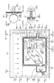
図1は、本発明に係る第1の実施形態の露光装置の全体構成を示す側面図(a)、A方向からみた矢視図(b)、B部の詳細図(c)である。
[First Embodiment]
FIG. 1 is a side view (a) showing the overall configuration of the exposure apparatus of the first embodiment according to the present invention, an arrow view (b) viewed from the direction A, and a detailed view (c) of part B.
図1において、100は光源部、12は光源部100を囲む真空容器、21は真空容器12内を真空雰囲気にするための真空ポンプ、22は真空容器12と真空ポンプ21を連結する結合部材である。
In FIG. 1, 100 is a light source unit, 12 is a vacuum vessel surrounding the
また、200は照明光学系(鏡筒)、400は投影光学系(鏡筒)、350はマスク300を駆動するマスクステージ、550は被処理体(ウエハ)500を駆動するウエハステージである。更に、14は上記各構成物を囲む真空容器、23は真空容器14内を真空雰囲気にするための真空ポンプ、24は真空容器14と真空ポンプ23とを連結する結合部材である。
ここで、光源部100、照明光学系200、及び投影光学系400について図4を用いて詳細に説明する。
Here, the
図4において、露光装置10は露光用の照明光としてEUV光(例えば、波長13.4nm)を用いてステップ・アンド・スキャン方式の投影露光を行い、光源部100、照明光学系200、マスク300、投影光学系400、被処理体500を有する。また、露光装置10は、マスク300を載置するマスクステージ350及び被処理体500を載置するウエハステージ550を更に有し、マスクステージ350とウエハステージ550は図示しない制御部に接続されて駆動制御される。
In FIG. 4, an
真空容器12内で発生したEUV光束160は、窓部210を通って照明光学系200及び投影光学系400が配置されている真空容器14内に入る。その後、照明光学系200のミラー群で反射し、ミラー286で跳ね上げられてマスク300に入射する。そして、このマスク300上のパターンが投影光学系400を通じて被処理体(ウエハ)500に結像する。
The EUV
図1の説明に戻り、真空容器14の内壁付近には、光源部100から光を通す窓部210、真空ポンプ23が結合部材24を介して取り付けられている部分等を除いて、全面に熱吸収板26が配置されている。更に熱吸収板26は熱伝導部材33を介して真空容器14の壁部に熱交換可能に連結されている。
Returning to the description of FIG. 1, near the inner wall of the
上記構成を詳細に示したのが図1(c)である。熱伝導部材33は、例えば両端に雄ネジが切ってあり、一端を真空容器14の壁部に形成された雌ネジにねじ込み、他端は熱吸収板26をはめ込んだ後、ナット35で締結する。
FIG. 1C shows the above configuration in detail. The
また、別の構成として、熱吸収板26と真空容器14の壁部の間にインジウム等の熱伝導率の大きい、柔らかい金属で埋め、熱吸収板26をネジ等で真空容器14の壁部に締結しても良い。柔らかいという条件は、熱吸収板26及び真空容器14の壁部に密着させるために必要である。
As another configuration, the
以上の例の他、熱吸収板26が真空容器14の壁部に熱交換可能に連結されていれば別の形態でも良い。
In addition to the above example, another form may be used as long as the
熱吸収板26に求められる条件は、真空容器14内部に向く面の輻射率が大きいことと熱吸収板26の母材の熱伝導率が大きいことである。この条件は、例えば、母材を銅(熱伝導率:403W/m・K)或いはアルミニウム(熱伝導率:238W/m・K)とし、表面処理として、Al2O3(アルミナセラミクス、輻射率:0.6程度)或いはAl2O3とSiO2の混合物(輻射率:0.85程度)を溶射することで達成される。
The conditions required for the
また、熱伝導部材33に求められる条件は、熱伝導率が大きいことである。これは例えば銅(熱伝導率:403W/m・K)、アルミニウム(熱伝導率:238W/m・K)或いはSiC(熱伝導率:150W/m・K)で達成される。
Moreover, the conditions calculated | required by the heat
更に真空容器14の壁部も熱伝導率が大きいほうが良いので、例えばアルミニウム(熱伝導率:238W/m・K)を用いることでこの条件が達成される。
Furthermore, since it is preferable that the wall portion of the
真空容器14は、温調チャンバ27の中に配置される。温調チャンバ27からは、一定の温度に管理された空気流31が噴き出している。一定の温度とは、投影光学系400内、或いは照明光学系200内の温度がゼロクロス温度になる温度が考えられる。なお、上記空気流31に代えて、ゼロクロス温度に管理された他の冷却媒体(不活性ガス等)を用いて熱を取り去っても良い。
The
投影光学系(鏡筒)400内には、鏡筒内温度センサ39が配置されており、その温度情報が温調チャンバ27の温度制御を行う温調チャンバ温度制御部38に伝えられる。そして、例えば、鏡筒内温度センサ39が検出した鏡筒内の温度がゼロクロス温度より高ければ温調チャンバ27から噴き出す空気流31の温度を下げることで、投影光学系(鏡筒)400内の温度をゼロクロス温度にすることが可能となる。
In the projection optical system (lens barrel) 400, a
また、投影光学系400内の温度と真空容器14外の温度との相互関係が予めわかれば、鏡筒内温度センサ39の検出温度を温調チャンバ温度制御部38にフィードバックするのではなく、真空容器壁温度センサ40の検出温度をフィードバックしても良い。更に、フィードバック制御の基本情報となる温度は、鏡筒内温度センサ39ではなく、不図示の照明光学系(鏡筒)200内に配置された温度センサでも良い。
Further, if the correlation between the temperature in the projection
上記真空容器14内に配置される照明光学系200及び投影光学系400の各ミラーは、一定の温度環境で使用されることが好ましい。なぜならば、温度が変化することで、面変形が起こり、その変形の大きさが変化し収差変動を引き起こすからである。特に、ミラーの中でもEUV露光装置で使用する可能性の高い低熱膨張ガラスで代表的なゼロデュア(SHOTT製)はその熱膨張率が室温付近でゼロとなる温度(ゼロクロス温度)が存在する。よって、その温度にて一定に保つことで面変形をゼロ(或いは低減)させることが可能となるので、温度をゼロクロス温度に保つことはなおさら重要である。
The mirrors of the illumination
しかしながら、真空容器14内では様々な要因により熱が発生し温度が上昇する。
However, heat is generated in the
先ず考えられるのは、露光光がミラーに照射されることで発生する熱や、照明光学系200及び投影光学系400内に配置されるミラー駆動用のアクチュエータや、ミラー位置計測用センサから発生される、真空容器14の内部で発生する熱である。
First of all, the heat generated when the exposure light is applied to the mirror, the mirror driving actuator disposed in the illumination
これらの熱は、発生すると、最終的には輻射熱となり、真空容器14の内壁付近に配置された熱吸収板26に達する。そしてその熱は熱伝導部材33、真空容器14の壁部を通って真空容器14の外壁に達する。真空容器14の外壁は、温調チャンバ27から噴き出されている空気流31にさらされているので、その熱が取り去られ、一定の温度に管理された空気流31によって、真空容器14内の温度は一定になる。
When these heats are generated, they eventually become radiant heat and reach the
次に考えられるのは、真空容器14に取り付けられた真空ポンプ23等、外部からの熱である。図1(b)に示すように、この熱34は投影光学系400等に輻射熱として達する場合がある。光学系に達した熱は、投影光学系400内に配置されたミラーの温度を上昇させ、面変形を悪化させることになる。
The next possibility is heat from the outside such as the
このような問題を解決するためには、投影光学系400の外壁に少なくとも一部を輻射率の小さい(反射率の大きい)熱反射板32で覆えば良い。こうすることで、投影光学系400に達した熱は熱反射板32で反射され、熱吸収板26に達する。その後は内部から発生する熱と同様になるので、その原理や効果等に関する説明は省略する。
In order to solve such a problem, at least a part of the outer wall of the projection
上記熱反射板32は、真空ポンプ23からの熱など、外部からの輻射熱に対して効果的な部分に配置することが重要である。本実施形態では、投影光学系400付近に設けたが、露光装置全体の配置から、効果的な場所が照明光学系200である場合は照明光学系200の外壁に、或いは、照明光学系200及び投影光学系400両方に配置すれば良い。
It is important to arrange the
また、熱反射板32は、投影光学系400の鏡筒に、別部材で取り付けられるようにしても良いし、或いは、投影光学系400の鏡筒そのものが輻射率の小さい部材で構成されていても良い。
In addition, the
以上のように、真空容器14内で発生する熱も、真空容器14外で発生する熱も、最終的に熱吸収板26に達し、熱伝導部材33及び真空容器14を通じて外壁に至り、一定温度に管理された温調チャンバ27からの空気流31に晒される。このため、真空容器14内部の温度はゼロクロス温度で一定に保つことが可能となる。よって、温度変化に起因するミラー部材の変形による収差変動をゼロ或いは低減することが可能となる。
As described above, the heat generated inside the
[第2の実施形態]
第2の実施形態は、特に真空容器14外で発生する真空ポンプ23からの熱を効果的に取り去る構成に関するものである。
[Second Embodiment]
The second embodiment particularly relates to a configuration that effectively removes heat from the
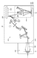
図2は、本発明に係る第2の実施形態として、図1のC部を詳細に示す図である。 FIG. 2 is a diagram showing in detail the portion C of FIG. 1 as a second embodiment according to the present invention.
図2において、真空ポンプ23と真空容器14とを連結する結合部材24の内壁には表面処理層30が形成されている。表面処理層30に求められる条件とは、輻射率の大きいことである。これは、第1の実施形態でも説明した通り、Al2O3(アルミナセラミクス、輻射率:0.6程度)或いは、Al2O3とSiO2の混合物(輻射率:0.85程度)を溶射することで達成される。
In FIG. 2, a
このような構成にすれば、真空ポンプ23で発生した熱34は、表面処理層30で吸収されて結合部材24の外壁に達し、温調チャンバ27から噴き出される空気流31にて冷却される。このため、熱34は真空容器14内部に侵入することが無くなる、或いは低減され、真空容器14内部の温度環境をゼロクロス温度にて一定にする効果が高くなる。
With this configuration, the
本実施形態では、結合部材24の冷却を温調チャンバ27からの空気流31として説明したが、冷却ジャケットを結合部材24に巻き、ゼロクロス温度に管理された冷却媒体を流すことで熱34を取り去っても良い。また、結合部材24の内壁を輻射率の大きい表面処理層30で覆う構成にしているが、図1(a)に示すような、熱伝導部材33を介して熱吸収板26を結合部材24の内壁付近に配置しても良い。
In the present embodiment, the cooling of the
[第3の実施形態]
第3の実施形態は、真空容器14の冷却に空気流31ではなく、冷却ジャケット25を用いている点で第1の第1の実施形態と相違している。
[Third Embodiment]
The third embodiment is different from the first embodiment in that the cooling jacket 25 is used instead of the air flow 31 for cooling the
図3は、本発明に係る第3の実施形態の露光装置の全体構成を示す側面図(a)及び真空容器に配された冷却ジャケットの図(b)である。なお、以下では、図1と同一の構成には同一の符号を付して説明は省略する。 FIG. 3A is a side view showing the overall configuration of an exposure apparatus according to the third embodiment of the present invention, and FIG. 3B is a view of a cooling jacket arranged in the vacuum vessel. In the following, the same components as those in FIG.
図3に示すように、真空容器14内部或いは外部で発生した熱は、熱吸収板26及び熱伝導部材33を介して真空容器14の壁部に達する。
As shown in FIG. 3, the heat generated inside or outside the
真空容器14の外部は、熱交換可能に連結された冷却ジャケット25で覆われている。冷却ジャケット25は、具体的には、図3(b)に示すように、パイプ25A及びチューブ25Bから成り立っており、その中をチラー36で温度制御された冷却媒体が流通している。冷却媒体としては、水等の熱容量の大きい流体が良い。
The outside of the
チラー36の役目は、冷却媒体を一定に保つことで投影光学系400或いは照明光学系200内をゼロクロス温度にすることと、その冷却媒体を供給管28を介して供給すると共に回収管29を介して回収し循環させることである。
The role of the
投影光学系(鏡筒)400内には、鏡筒内温度センサ39が配置されており、その温度情報がチラー36の温度制御を行うチラー温度制御部41に伝えられる。そして、例えば、鏡筒内温度センサ39が検出した鏡筒内の温度がゼロクロス温度より高ければチラー36から流す冷却媒体の温度を下げることで、投影光学系(鏡筒)400内の温度をゼロクロス温度にすることが可能となる。
A
また、投影光学系400内の温度と真空容器14外の温度との相互関係が予めわかっていれば、鏡筒内温度センサ39の検出温度をチラー温度制御部41にフィードバックするのではなく、真空容器壁温度センサ40の検出温度をフィードバックしても良い。
Further, if the correlation between the temperature in the projection
更に、フィードバック制御の基本情報となる温度は、投影光学系(鏡筒)400内に配置された鏡筒内温度センサ39ではなく、不図示の照明光学系(鏡筒)200内に配置された温度センサでも良い。
Furthermore, the temperature that is the basic information of the feedback control is arranged not in the lens
以上のように、真空容器14内で発生する熱も、真空容器14外で発生する熱も、最終的に熱吸収板26に達し、熱伝導部材33、真空容器14を通じて外壁に至り、一定温度に管理されたチラー36からの冷却媒体が通る冷却ジャケット25に触れる。このため、投影光学系(鏡筒)400内の温度、或いは照明光学系(鏡筒)200内の温度はゼロクロス温度で一定に保つことが可能となる。よって、温度変化に起因するミラー部材の変形による収差変動をゼロ或いは低減することが可能となる。
As described above, the heat generated inside the
[デバイス製造方法]
次に、上述した露光装置を利用したデバイス製造方法の実施形態を説明する。
[Device manufacturing method]
Next, an embodiment of a device manufacturing method using the above-described exposure apparatus will be described.
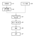
図6は微小デバイス(ICやLSI等の半導体チップ、液晶パネル、CCD、薄膜磁気ヘッド、マイクロマシン等)の製造のフローを示す。ステップS1(回路設計)では半導体デバイスの回路設計を行う。ステップS2(露光制御データ作成)では設計した回路パターンに基づいて露光装置の露光制御データを作成する。一方、ステップS3(ウエハ製造)ではシリコン等の材料を用いてウエハを製造する。ステップS4(ウエハプロセス)は前工程と呼ばれ、上記用意した露光制御データが入力された露光装置とウエハを用いて、リソグラフィ技術によってウエハ上に実際の回路を形成する。次のステップS5(組み立て)は後工程と呼ばれ、ステップS4によって作製されたウエハを用いて半導体チップ化する工程であり、アッセンブリ工程(ダイシング、ボンディング)、パッケージング工程(チップ封入)等の工程を含む。ステップS6(検査)ではステップS5で作製された半導体デバイスの動作確認テスト、耐久性テスト等の検査を行う。こうした工程を経て半導体デバイスが完成し、これが出荷(ステップS7)される。 FIG. 6 shows a manufacturing flow of a microdevice (a semiconductor chip such as an IC or LSI, a liquid crystal panel, a CCD, a thin film magnetic head, a micromachine, etc.). In step S1 (circuit design), a semiconductor device circuit is designed. In step S2 (exposure control data creation), exposure control data for the exposure apparatus is created based on the designed circuit pattern. On the other hand, in step S3 (wafer manufacture), a wafer is manufactured using a material such as silicon. Step S4 (wafer process) is called a pre-process, and an actual circuit is formed on the wafer by lithography using the wafer and the exposure apparatus to which the prepared exposure control data is input. The next step S5 (assembly) is called a post-process, and is a process for forming a semiconductor chip using the wafer manufactured in step S4, and is a process such as an assembly process (dicing, bonding), a packaging process (chip encapsulation), or the like. including. In step S6 (inspection), inspections such as an operation confirmation test and a durability test of the semiconductor device manufactured in step S5 are performed. Through these steps, the semiconductor device is completed and shipped (step S7).
図7は上記ウエハプロセスの詳細なフローを示す。ステップS11(酸化)ではウエハの表面を酸化させる。ステップS12(CVD)ではウエハ表面に絶縁膜を形成する。ステップS13(電極形成)ではウエハ上に電極を蒸着によって形成する。ステップS14(イオン打込み)ではウエハにイオンを打ち込む。ステップS15(レジスト処理)ではウエハに感光剤を塗布する。ステップS16(露光)では上記説明した露光装置によって回路パターンをウエハに焼付露光する。ステップS17(現像)では露光したウエハを現像する。ステップ18(エッチング)では現像したレジスト像以外の部分を削り取る。ステップS19(レジスト剥離)ではエッチングが済んで不要となったレジストを取り除く。これらのステップを繰り返し行うことによって、ウエハ上に多重に回路パターンが形成される。 FIG. 7 shows a detailed flow of the wafer process. In step S11 (oxidation), the wafer surface is oxidized. In step S12 (CVD), an insulating film is formed on the wafer surface. In step S13 (electrode formation), an electrode is formed on the wafer by vapor deposition. In step S14 (ion implantation), ions are implanted into the wafer. In step S15 (resist process), a photosensitive agent is applied to the wafer. In step S16 (exposure), the circuit pattern is printed on the wafer by exposure using the exposure apparatus described above. In step S17 (development), the exposed wafer is developed. In step 18 (etching), portions other than the developed resist image are removed. In step S19 (resist stripping), the resist that has become unnecessary after the etching is removed. By repeatedly performing these steps, multiple circuit patterns are formed on the wafer.
12,14:真空容器
21,23:真空ポンプ
22,24:結合部材
25:冷却ジャケット
25A:パイプ
25B:チューブ
26:熱吸収板
27:温調チャンバ
28:供給管
29:回収管
30:表面処理層
31:空気流
32:熱反射板
33:熱伝導部材
34:熱
35:ナット
36:チラー
37:窓
38:温調チャンバ温度制御部
39:鏡筒内温度センサ
40:真空容器壁温度センサ
41:チラー温度制御部
100:光源部
200:照明光学系(鏡筒)
210:窓部
300:マスク
350:マスクステージ
400:投影光学系(鏡筒)
500:被処理体(ウエハ)
550:ウエハステージ
12, 14:
210: Window portion 300: Mask 350: Mask stage 400: Projection optical system (lens barrel)
500: Object to be processed (wafer)
550: Wafer stage
Claims (9)
前記原版を照明する照明光を照射する照明光学系と、
前記照明光により照明された前記パターンを前記基板に投影する投影光学系と、
前記照明光学系及び前記投影光学系の少なくともいずれかを収容する真空容器と、を備え、
前記照明光学系及び前記投影光学系の少なくともいずれかの温度変化を抑制するために、前記真空容器内で発生する熱及び外部から前記真空容器内に入り込む熱を吸収する吸熱手段を設けたことを特徴とする露光装置。 An exposure apparatus that exposes an original pattern onto a substrate,
An illumination optical system for illuminating illumination light for illuminating the original plate;
A projection optical system that projects the pattern illuminated by the illumination light onto the substrate;
A vacuum vessel that houses at least one of the illumination optical system and the projection optical system,
In order to suppress a temperature change of at least one of the illumination optical system and the projection optical system, a heat absorption means for absorbing heat generated in the vacuum container and heat entering the vacuum container from the outside is provided. A featured exposure apparatus.
この輻射熱を、前記真空容器と前記真空ポンプを連結する結合部材で吸収し、当該結合部材を前記チャンバから噴き出される空気流又は冷却媒体により冷却することを特徴とする請求項1又は2に記載の露光装置。 The heat entering the vacuum container is radiant heat of a vacuum pump connected to the vacuum container,
The radiant heat is absorbed by a coupling member connecting the vacuum vessel and the vacuum pump, and the coupling member is cooled by an air flow or a cooling medium ejected from the chamber. Exposure equipment.
前記照明光学系及び投影光学系は、前記極端紫外線領域又はX線領域の光を反射させるミラー部材で構成されていることを特徴とする請求項1乃至7のいずれか1項に記載の露光装置。 The illumination optical system generates light in the extreme ultraviolet region or X-ray region having a wavelength of 200 nm to 10 nm,
The exposure apparatus according to claim 1, wherein the illumination optical system and the projection optical system are configured by a mirror member that reflects light in the extreme ultraviolet region or the X-ray region. .
Priority Applications (4)
| Application Number | Priority Date | Filing Date | Title |
|---|---|---|---|
| JP2005334464A JP2007142190A (en) | 2005-11-18 | 2005-11-18 | Exposure system and device manufacturing method |
| US11/558,148 US7804578B2 (en) | 2005-11-18 | 2006-11-09 | Exposure apparatus and device manufacturing method |
| EP06023556A EP1788447A3 (en) | 2005-11-18 | 2006-11-13 | Exposure apparatus and device manufacturing method |
| KR1020060113670A KR100839859B1 (en) | 2005-11-18 | 2006-11-17 | Exposure apparatus and device manufacturing method |
Applications Claiming Priority (1)
| Application Number | Priority Date | Filing Date | Title |
|---|---|---|---|
| JP2005334464A JP2007142190A (en) | 2005-11-18 | 2005-11-18 | Exposure system and device manufacturing method |
Publications (1)
| Publication Number | Publication Date |
|---|---|
| JP2007142190A true JP2007142190A (en) | 2007-06-07 |
Family
ID=37846925
Family Applications (1)
| Application Number | Title | Priority Date | Filing Date |
|---|---|---|---|
| JP2005334464A Withdrawn JP2007142190A (en) | 2005-11-18 | 2005-11-18 | Exposure system and device manufacturing method |
Country Status (4)
| Country | Link |
|---|---|
| US (1) | US7804578B2 (en) |
| EP (1) | EP1788447A3 (en) |
| JP (1) | JP2007142190A (en) |
| KR (1) | KR100839859B1 (en) |
Cited By (4)
| Publication number | Priority date | Publication date | Assignee | Title |
|---|---|---|---|---|
| JP2010056233A (en) * | 2008-08-27 | 2010-03-11 | Canon Inc | Exposure apparatus and device manufacturing method |
| JP2010129687A (en) * | 2008-11-26 | 2010-06-10 | Nikon Corp | Vacuum apparatus, light source apparatus, exposure apparatus, and method of manufacturing device |
| JP2011029511A (en) * | 2009-07-28 | 2011-02-10 | Nikon Corp | Optical system, exposure device and method of manufacturing device |
| JP2019212465A (en) * | 2018-06-04 | 2019-12-12 | 株式会社ニューフレアテクノロジー | Vacuum apparatus |
Families Citing this family (9)
| Publication number | Priority date | Publication date | Assignee | Title |
|---|---|---|---|---|
| JP5103060B2 (en) * | 2007-06-05 | 2012-12-19 | 東京応化工業株式会社 | Cooling apparatus and substrate processing apparatus |
| WO2009039883A1 (en) * | 2007-09-26 | 2009-04-02 | Carl Zeiss Smt Ag | Optical imaging device with thermal stabilization |
| JP5495547B2 (en) * | 2008-12-25 | 2014-05-21 | キヤノン株式会社 | Processing apparatus and device manufacturing method |
| US8872142B2 (en) | 2010-03-18 | 2014-10-28 | Gigaphoton Inc. | Extreme ultraviolet light generation apparatus |
| KR102002269B1 (en) * | 2010-07-30 | 2019-07-19 | 칼 짜이스 에스엠티 게엠베하 | Euv exposure apparatus |
| DE102011086457A1 (en) * | 2011-11-16 | 2012-12-20 | Carl Zeiss Smt Gmbh | Extreme UV imaging device e.g. extreme UV lithography system, for manufacturing integrated circuits, has sensor device detecting measuring variable and formed as fiber Bragg lattice sensor |
| CN110291462B (en) * | 2017-02-01 | 2021-07-20 | 卡尔蔡司Smt有限责任公司 | Device and method for operating a device |
| US10943761B2 (en) | 2017-03-07 | 2021-03-09 | Asml Netherlands B.V. | System for evacuating a chamber |
| NL2020353A (en) * | 2017-04-11 | 2018-10-17 | Asml Netherlands Bv | Lithographic apparatus |
Family Cites Families (10)
| Publication number | Priority date | Publication date | Assignee | Title |
|---|---|---|---|---|
| US5877843A (en) * | 1995-09-12 | 1999-03-02 | Nikon Corporation | Exposure apparatus |
| AU1053199A (en) * | 1997-11-14 | 1999-06-07 | Nikon Corporation | Exposure apparatus and method of manufacturing the same, and exposure method |
| US6630984B2 (en) | 2000-08-03 | 2003-10-07 | Asml Netherlands B.V. | Lithographic apparatus, device manufacturing method, and device manufactured thereby |
| JP2002248344A (en) * | 2001-02-26 | 2002-09-03 | Nikon Corp | Extreme ultraviolet light generator as well as exposure device and method for manufacturing semiconductor using the same |
| JP2003142395A (en) * | 2001-11-08 | 2003-05-16 | Canon Inc | Temperature-controlled fluid supplying apparatus, aligner comprising the apparatus, and method of manufacturing semiconductor device |
| TW589915B (en) * | 2002-05-24 | 2004-06-01 | Sanyo Electric Co | Electroluminescence display device |
| JP4065528B2 (en) | 2003-03-10 | 2008-03-26 | キヤノン株式会社 | Constant temperature vacuum container and exposure apparatus using the same |
| JP2004336026A (en) * | 2003-04-15 | 2004-11-25 | Canon Inc | Thermostat, exposure device having the same, and manufacturing method of device |
| EP1491955A1 (en) | 2003-06-27 | 2004-12-29 | ASML Netherlands B.V. | Lithographic projection apparatus and device manufacturing method |
| JP2005142382A (en) * | 2003-11-07 | 2005-06-02 | Canon Inc | Exposure apparatus |
-
2005
- 2005-11-18 JP JP2005334464A patent/JP2007142190A/en not_active Withdrawn
-
2006
- 2006-11-09 US US11/558,148 patent/US7804578B2/en not_active Expired - Fee Related
- 2006-11-13 EP EP06023556A patent/EP1788447A3/en not_active Withdrawn
- 2006-11-17 KR KR1020060113670A patent/KR100839859B1/en active IP Right Grant
Cited By (5)
| Publication number | Priority date | Publication date | Assignee | Title |
|---|---|---|---|---|
| JP2010056233A (en) * | 2008-08-27 | 2010-03-11 | Canon Inc | Exposure apparatus and device manufacturing method |
| JP2010129687A (en) * | 2008-11-26 | 2010-06-10 | Nikon Corp | Vacuum apparatus, light source apparatus, exposure apparatus, and method of manufacturing device |
| JP2011029511A (en) * | 2009-07-28 | 2011-02-10 | Nikon Corp | Optical system, exposure device and method of manufacturing device |
| JP2019212465A (en) * | 2018-06-04 | 2019-12-12 | 株式会社ニューフレアテクノロジー | Vacuum apparatus |
| JP7163073B2 (en) | 2018-06-04 | 2022-10-31 | 株式会社ニューフレアテクノロジー | vacuum equipment |
Also Published As
| Publication number | Publication date |
|---|---|
| US7804578B2 (en) | 2010-09-28 |
| KR100839859B1 (en) | 2008-06-20 |
| EP1788447A3 (en) | 2009-12-09 |
| EP1788447A2 (en) | 2007-05-23 |
| US20070115444A1 (en) | 2007-05-24 |
| KR20070053134A (en) | 2007-05-23 |
Similar Documents
| Publication | Publication Date | Title |
|---|---|---|
| JP2007142190A (en) | Exposure system and device manufacturing method | |
| US10324383B2 (en) | Chucks and clamps for holding objects of a lithographic apparatus and methods for controlling a temperature of an object held by a clamp of a lithographic apparatus | |
| US10191395B2 (en) | Thermal conditioning unit, lithographic apparatus and device manufacturing method | |
| TWI434132B (en) | Euv reticle substrates with high thermal conductivity | |
| JP2004363559A (en) | Optical member holder | |
| JP2005109158A (en) | Cooling apparatus and method therefor, aligner equipped therewith, and manufacturing method of device | |
| JP2006216733A (en) | Exposure apparatus, manufacturing method of optical element, and device manufacturing method | |
| JP2007048881A (en) | Vacuum exposure apparatus | |
| US20090103063A1 (en) | Cooling apparatus for optical member, barrel, exposure apparatus, and device manufacturing method | |
| US7397531B2 (en) | Lithographic apparatus and device manufacturing method | |
| EP1569036B1 (en) | Exposure apparatus and device manufacturing method | |
| JP2004095993A (en) | Method for cooling optical component, apparatus for cooling optical component, and euv exposure system employing the apparatus | |
| JP4458323B2 (en) | Holding apparatus, exposure apparatus having the holding apparatus, and device manufacturing method | |
| JP4532835B2 (en) | Cooling device, optical member having the same, and exposure apparatus | |
| US20050128448A1 (en) | Lithographic apparatus and device manufacturing method | |
| JP2006100363A (en) | Aligner, exposure method, and device manufacturing method | |
| JP2004246030A (en) | Optical element, optical element holding device, temperature adjusting device, aligner and manufacturing method of device | |
| JP2006073895A (en) | Cooling device, aligner, and device manufacturing method | |
| JP4393227B2 (en) | Exposure apparatus, device manufacturing method, and exposure apparatus manufacturing method | |
| JP3526162B2 (en) | Substrate holding device and exposure device | |
| JP4893249B2 (en) | Exposure apparatus and method for manufacturing semiconductor device or liquid crystal device using the same | |
| JP4393226B2 (en) | Optical system, exposure apparatus using the same, and device manufacturing method | |
| JP4537087B2 (en) | Exposure apparatus and device manufacturing method | |
| JP2012231046A (en) | Optical apparatus, exposure apparatus, and device manufacturing method | |
| JP2004247473A (en) | Cooling device and method, and aligner including the same |
Legal Events
| Date | Code | Title | Description |
|---|---|---|---|
| A621 | Written request for application examination |
Free format text: JAPANESE INTERMEDIATE CODE: A621 Effective date: 20081117 |
|
| A761 | Written withdrawal of application |
Free format text: JAPANESE INTERMEDIATE CODE: A761 Effective date: 20100120 |