JP2007134635A - Semiconductor device and manufacturing method thereof - Google Patents
Semiconductor device and manufacturing method thereof Download PDFInfo
- Publication number
- JP2007134635A JP2007134635A JP2005328652A JP2005328652A JP2007134635A JP 2007134635 A JP2007134635 A JP 2007134635A JP 2005328652 A JP2005328652 A JP 2005328652A JP 2005328652 A JP2005328652 A JP 2005328652A JP 2007134635 A JP2007134635 A JP 2007134635A
- Authority
- JP
- Japan
- Prior art keywords
- semiconductor device
- layer
- substrate
- base layer
- semiconductor substrate
- Prior art date
- Legal status (The legal status is an assumption and is not a legal conclusion. Google has not performed a legal analysis and makes no representation as to the accuracy of the status listed.)
- Pending
Links
Images
Classifications
-
- H—ELECTRICITY
- H10—SEMICONDUCTOR DEVICES; ELECTRIC SOLID-STATE DEVICES NOT OTHERWISE PROVIDED FOR
- H10W—GENERIC PACKAGES, INTERCONNECTIONS, CONNECTORS OR OTHER CONSTRUCTIONAL DETAILS OF DEVICES COVERED BY CLASS H10
- H10W72/00—Interconnections or connectors in packages
- H10W72/01—Manufacture or treatment
- H10W72/012—Manufacture or treatment of bump connectors, dummy bumps or thermal bumps
Landscapes
- Internal Circuitry In Semiconductor Integrated Circuit Devices (AREA)
Abstract
【課題】強度を高めて、熱ストレスなどによりクラックが入るのを抑制できるハンダバンプを有する半導体装置と、その製造方法を提供する。
【解決手段】電子回路が形成された半導体基板に、電子回路に電気的に接続され、半導体基板の表面から突出して下地層が形成されており、下地層の基板の表面から突出して形成された部分の表面に接合してハンダからなるバンプが形成されている構成とする。
【選択図】図1The present invention provides a semiconductor device having a solder bump capable of increasing strength and suppressing cracking due to thermal stress and the like, and a method for manufacturing the same.
A semiconductor substrate on which an electronic circuit is formed is electrically connected to the electronic circuit, and a base layer is formed protruding from the surface of the semiconductor substrate, and the base layer is formed protruding from the surface of the substrate. A bump made of solder is formed by bonding to the surface of the part.
[Selection] Figure 1
Description
本発明は、半導体装置およびその製造方法に関し、特に、ハンダバンプを有する半導体装置およびその製造方法に関する。 The present invention relates to a semiconductor device and a manufacturing method thereof, and more particularly to a semiconductor device having solder bumps and a manufacturing method thereof.
デジタルビデオカメラ、デジタル携帯電話、あるいはノートパソコンなど、携帯用電子機器の小型化、薄型化、軽量化に対する要求は強くなる一方であり、これに応えるために近年のVLSIなどの半導体装置においては3年で7割の縮小化を実現してきた一方で、このような半導体装置をプリント配線基板上に実装した電子回路装置としても、実装基板(プリント配線基板)上の部品実装密度をいかに向上させるかが重要な課題として研究および開発がなされてきた。 The demand for downsizing, thinning, and weight reduction of portable electronic devices such as digital video cameras, digital mobile phones, and notebook personal computers is increasing. While an electronic circuit device in which such a semiconductor device is mounted on a printed wiring board has been realized by 70% reduction year by year, how can the component mounting density on the mounting substrate (printed wiring substrate) be improved? Has been researched and developed as an important issue.
例えば、半導体装置のパッケージ形態としては、DIP(Dual Inline Package )などのリード挿入型から表面実装型へと移行し、さらには半導体チップのパッド電極にハンダや金などからなるバンプ(突起電極)を設け、フェースダウンでバンプを介して配線基板に接続するフリップチップ実装法が開発された。 For example, the package form of a semiconductor device has shifted from a lead insertion type such as DIP (Dual Inline Package) to a surface mount type, and furthermore, bumps (projection electrodes) made of solder, gold, etc. are provided on the pad electrodes of the semiconductor chip. A flip-chip mounting method has been developed in which a face-down connection is made to the wiring board via bumps.
上記のようにフリップチップで実装するような半導体装置の小型のパッケージング方法としてCSP(チップサイズパッケージ)が開発されている。
さらにリアルチップサイズのパッケージング方法として、ウェーハレベルのCSP(WL−CSP)が提案されている。ここでは、インターポーザ基板を用いたCSPの代わりに、LSIの外部端子がアクティブエリア上でエリアアレイ状に再配線され、各配線にハンダなどのバンプが形成されている。
上記のようなハンダバンプが形成されてフリップチップで実装するタイプの半導体装置として、例えば、特許文献1に上記のSiP形態の半導体装置が開示されている。
As described above, CSP (chip size package) has been developed as a small packaging method for semiconductor devices to be mounted by flip chip.
Further, a wafer level CSP (WL-CSP) has been proposed as a real chip size packaging method. Here, instead of the CSP using the interposer substrate, the external terminals of the LSI are rewired in the form of an area array on the active area, and bumps such as solder are formed on each wiring.
As a semiconductor device of the type in which the solder bump as described above is formed and mounted by flip chip, for example, Patent Document 1 discloses the above-described SiP type semiconductor device.
従来技術においては、上記のハンダバンプは、例えば以下のようにして形成される。
まず、図6(a)に示すように、電子回路などの素子が形成された半導体基板100の表面にAlなどからなるパッド電極101が形成されており、化学気相成長(CVD)法などにより全面に窒化シリコンを堆積して保護膜102を形成し、パッド電極101部分を開口する開口部102aをパターン形成する。
In the prior art, the solder bump is formed as follows, for example.
First, as shown in FIG. 6A, a
次に、図6(b)に示すように、逆スッパタリング法により、開口部102aにおいて露出しているパッド電極101を被覆して全面にシード層となるTi層103を形成し、さらにその上層に同じくシード層となるCu層104aを形成する。
Next, as shown in FIG. 6B, a
次に、図7(a)に示すように、Cu層104aを被覆して全面に感光性ドライフィルムを貼付け、フォトリソグラフィ工程によりバンプ形成領域を開口するパターンで露光及び現像処理を行い、マスク層105をパターン形成する。
Next, as shown in FIG. 7A, a
次に、図7(b)に示すように、マスク層105の開口部内において、Ti層103及びCu層104aを一方の電極とする電解メッキ処理により、Cu層104aの上層にCuを堆積させ、厚膜化したCu層104とする。
さらに、電解メッキ処理により、Cu層104の上層にNi層106を形成し、さらにAu層107を形成する。
Next, as shown in FIG. 7B, Cu is deposited on the upper layer of the
Further, the
次に、図8(a)に示すように、溶剤またはアッシング処理により、マスク層105を剥離除去する。
Next, as shown in FIG. 8A, the
次に、図8(b)に示すように、Au層107をマスクとするエッチング処理により、下層のCu層104及びTi層103を順にAu層107と同じパターンに加工し、洗浄処理を行う。
Next, as shown in FIG. 8B, the
次に、図9(a)に示すように、スピンコート法によりAu層107の表面を被覆するような膜厚で、ポリイミド(PI)やベンゾシクロブテン(BCB)などの感光性の絶縁樹脂を全面に塗布し、プリベーク処理を行い、バンプ形成領域を開口するパターンで露光及び現像処理を行ってAu層107を露出させ、さらにポストベーク処理及びアッシング処理を行う。これにより、バンプ形成領域において開口するパターンの絶縁樹脂層108を形成する。絶縁樹脂層108の開口部はAu層107の上面よりも狭くなるようなレイアウトとする。
Next, as shown in FIG. 9A, a photosensitive insulating resin such as polyimide (PI) or benzocyclobutene (BCB) is formed with a film thickness that covers the surface of the
次に、図9(b)に示すように、絶縁樹脂層108に開口した開口部内にフラックスを印刷し、さらにハンダボールを供給する。次に、リフロー処理を行うことで、ハンダボールを一度溶融させ、Au層107の表面とハンダボール表面を接合させて、ハンダバンプ109を形成する。この後、フラックスを除去するための洗浄処理を行う。
以上の方法により、ハンダバンプを形成できる。
Next, as shown in FIG. 9B, a flux is printed in the opening portion opened in the
Solder bumps can be formed by the above method.
しかしながら、上記の従来のハンダバンプは、絶縁樹脂層108の開口部はAu層107の上面よりも狭くなるようなレイアウトであり、ハンダバンプを形成するランドが絶縁層で絞り込まれるような構造となっているため、図9(b)に示すように、絶縁樹脂層との境界部分109rでハンダが括れた状態になり、このバンプが形成されたデバイスを実装基板に実装したとき、この括れた境界部分109rの強度が不十分となり、熱ストレスの影響でクラックが入ってしまう不具合が生じやすくなっていた。
本発明の目的は、強度を高めて、熱ストレスなどによりクラックが入るのを抑制できるハンダバンプを有する半導体装置と、その製造方法を提供することである。 An object of the present invention is to provide a semiconductor device having a solder bump that can increase the strength and suppress cracks due to thermal stress and the like, and a manufacturing method thereof.
上記の課題を解決するため、本発明の半導体装置は、電子回路が形成された半導体基板と、前記電子回路に電気的に接続され、前記半導体基板の表面から突出して形成された下地層と、前記下地層の前記基板の表面から突出して形成された部分の表面に接合して形成されたハンダからなるバンプとを有する。 In order to solve the above-described problems, a semiconductor device of the present invention includes a semiconductor substrate on which an electronic circuit is formed, a base layer that is electrically connected to the electronic circuit and protrudes from the surface of the semiconductor substrate, And a bump made of solder formed by bonding to a surface of a portion of the base layer that protrudes from the surface of the substrate.
上記の本発明の半導体装置は、電子回路が形成された半導体基板に、電子回路に電気的に接続され、半導体基板の表面から突出して下地層が形成されており、下地層の基板の表面から突出して形成された部分の表面に接合してハンダからなるバンプが形成されている。 In the semiconductor device of the present invention, a semiconductor substrate on which an electronic circuit is formed is electrically connected to the electronic circuit, and a base layer is formed protruding from the surface of the semiconductor substrate. A bump made of solder is formed by bonding to the surface of the protruding portion.
また、上記の課題を解決するため、本発明の半導体装置の製造方法は、電子回路が形成された半導体基板に、前記電子回路に電気的に接続して、前記半導体基板の表面から突出するように下地層を形成する工程と、前記下地層の前記基板の表面から突出して形成された部分の表面に接合して、ハンダからなるバンプを形成する工程とを有する。 In order to solve the above problems, a method of manufacturing a semiconductor device according to the present invention is such that a semiconductor substrate on which an electronic circuit is formed is electrically connected to the electronic circuit and protrudes from the surface of the semiconductor substrate. And forming a bump made of solder by bonding to the surface of the portion of the foundation layer that protrudes from the surface of the substrate.
上記の本発明の半導体装置の製造方法は、電子回路が形成された半導体基板に、電子回路に電気的に接続して、半導体基板の表面から突出するように下地層を形成する。
次に、下地層の基板の表面から突出して形成された部分の表面に接合して、ハンダからなるバンプを形成する。
In the method of manufacturing a semiconductor device according to the present invention, a base layer is formed on a semiconductor substrate on which an electronic circuit is formed so as to be electrically connected to the electronic circuit and protrude from the surface of the semiconductor substrate.
Next, a bump made of solder is formed by bonding to the surface of the portion of the base layer that protrudes from the surface of the substrate.
本発明の半導体装置は、ハンダバンプの強度が高められており、熱ストレスなどによりクラックが入るのを抑制できる。 In the semiconductor device of the present invention, the strength of the solder bumps is increased, and cracks due to thermal stress can be suppressed.
本発明の半導体装置の製造方法は、ハンダバンプの強度が高められ、熱ストレスなどによりクラックが入るのを抑制できる半導体装置を製造することができる。 The method for manufacturing a semiconductor device of the present invention can manufacture a semiconductor device in which the strength of solder bumps can be increased and cracks can be prevented from entering due to thermal stress or the like.
以下に、本発明の半導体装置及びその製造方法の実施の形態について、図面を参照して説明する。 Embodiments of a semiconductor device and a manufacturing method thereof according to the present invention will be described below with reference to the drawings.
第1実施形態
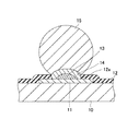
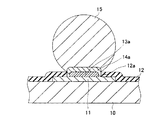
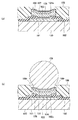
図1は本実施形態に係る半導体装置のバンプ部分の模式断面図である。
例えば、電子回路が形成された半導体基板10に、電子回路に電気的に接続されたAlなどからなるパッド電極11が形成されており、半導体基板10上にパッド電極11の一部を開口するパターンで開口部12aが形成された窒化シリコンなどからなる保護膜12が形成されている。
First Embodiment FIG. 1 is a schematic cross-sectional view of a bump portion of a semiconductor device according to this embodiment.
For example, a
上記の開口部12aの中央部において、パッド電極11の上層にAgナノペーストを固化してなる凸状層13が形成されており、凸状層13の上層において開口部12aの縁を外周とするパターンで、Niなどからなる下地層14が保護膜12の表面から突出して形成されている。
さらに、下地層14の保護膜12の表面から突出して形成された部分の表面に接合してハンダからなるバンプ15が形成されている。
A
Further, a
本実施形態においては、凸状層13の表面形状が頂部から外周部までなめらかに繋がる曲面を有しており、この凸状層13の表面形状を反映して、下地層14の保護膜12の表面から突出して形成された部分の表面形状が、頂部から外周部までなめらかに繋がる曲面を有している。
In the present embodiment, the surface shape of the
上記の構造を有するハンダバンプにおいて、バンプ15が下地層14の頂部から外周部までなめらかに繋がる曲面の全体において接合することにより、下地層14とバンプ15との界面とのせん断応力を大きくできるので、これにより下地層14とバンプ15の接合強度を高めることができる。
また、図9(b)に示す従来例のような、絶縁樹脂層でハンダバンプの下地の層との接合面積を規定してハンダバンプのネックが括れた構造とはならず、球状になることから、ヒートサイクルなどの熱ストレスに対して強い構造となっている。
上記のように、本実施形態に係る半導体装置のハンダバンプは、強度を高めて、熱ストレスなどによりクラックが入るのを抑制できる。
In the solder bump having the above structure, since the
Further, as in the conventional example shown in FIG. 9B, the insulating resin layer defines the bonding area with the underlying layer of the solder bump and does not have a structure in which the neck of the solder bump is constricted. The structure is strong against heat stress such as heat cycle.
As described above, the solder bump of the semiconductor device according to the present embodiment can increase the strength and suppress the occurrence of cracks due to thermal stress or the like.
次に、本実施形態に係る半導体装置の製造方法について説明する。
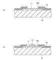
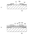
まず、図2(a)に示すように、例えば、電子回路が形成された半導体基板10に、電子回路に電気的に接続されたAlなどからなるパッド電極11を形成し、さらに例えばCVD法により窒化シリコンなどを堆積して、半導体基板10上にパッド電極11の一部を開口するパターンで開口部12aを形成し、保護膜12を形成する。
Next, a method for manufacturing the semiconductor device according to the present embodiment will be described.
First, as shown in FIG. 2A, for example, a
次に、図2(b)に示すように、例えば、開口部12aの中央部の開口部12aより狭い領域において、パッド電極11の上層に、Agナノペーストを印刷し、さらに加熱して固化し、凸状層13を形成する。
本実施形態においては、凸状層13の表面形状が、頂部から外周部までなめらかに繋がる曲面を有するように形成する。
Next, as shown in FIG. 2B, for example, in a region narrower than the
In the present embodiment, the surface shape of the
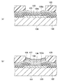
次に、図3(a)に示すように、例えば、ジンケート処理を行った後、さらにNiの無電解メッキ処理を行い、凸状層13の上層において開口部12aの縁を外周とするパターンで、Niなどからなる下地層14を保護膜12の表面から突出するようにして形成する。
ここでは、凸状層13の表面形状を反映して、下地層14の保護膜12の表面から突出して形成された部分の表面形状が、頂部から外周部までなめらかに繋がる曲面を有して形成される。
Next, as shown in FIG. 3A, for example, after a zincate process is performed, an electroless plating process of Ni is further performed so that the edge of the
Here, reflecting the surface shape of the
次に、図3(b)に示すように、下地層14の保護膜12の表面から突出して形成された部分の表面に接合して、ハンダからなるバンプ15を形成する。
以上で図1に示す構成のハンダバンプを有する半導体装置を形成することができる。
Next, as shown in FIG. 3B, the
Thus, a semiconductor device having solder bumps having the structure shown in FIG. 1 can be formed.
上記のようにして形成された半導体装置の下地層は、逆スパッタリング法により形成される従来のシードメタル層を介した構造と比較して、デバイスの端子電極との金属同士の接着が強く、且つ、下地層とハンダバンプとの界面のせん断応力が大きいことから、絶縁樹脂層で周辺部分を抑えるように補強する必要がなく、側面部分も露出した構造が取れる。 The base layer of the semiconductor device formed as described above has strong adhesion between metals with the terminal electrode of the device, as compared with a structure through a conventional seed metal layer formed by a reverse sputtering method, and Since the shear stress at the interface between the underlayer and the solder bump is large, there is no need to reinforce the peripheral portion with the insulating resin layer, and a structure in which the side portion is exposed can be taken.
また、絶縁樹脂層でハンダバンプと下地層が接合する面積を規定した場合のように、ハンダボールのネックが括れたような形状になることもなく、実装基板に実装した際に、ヒートサイクル等の熱ストレスにも、非常に強い構造となっている。
また、絶縁層の必要もなく、材料費、加工費のコストダウンも可能になる。
In addition, as in the case where the area where the solder bump and the base layer are joined is defined by the insulating resin layer, the neck of the solder ball is not constricted. It has a very strong structure against heat stress.
In addition, there is no need for an insulating layer, and material costs and processing costs can be reduced.
上記のように、本実施形態の半導体装置の製造方法は、ハンダバンプの強度が高められ、熱ストレスなどによりクラックが入るのを抑制できる半導体装置を製造することができる。 As described above, the semiconductor device manufacturing method of the present embodiment can manufacture a semiconductor device in which the strength of the solder bumps is increased and cracking due to thermal stress or the like can be suppressed.
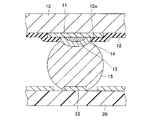
図4は、本実施形態のハンダバンプが形成された半導体装置を実装基板に実装したときのバンプ部分の模式断面図である。
実装基板は、実装基板本体20の表面に、配線21及び電極22などがパターン形成されている。
上記の電極とハンダバンプ15が接合するようにして、本実施形態の半導体装置がフリップチップで実装されている。
FIG. 4 is a schematic cross-sectional view of a bump portion when the semiconductor device on which the solder bump of this embodiment is formed is mounted on a mounting substrate.
The mounting substrate has a pattern of wiring 21 and
The semiconductor device of this embodiment is mounted on a flip chip so that the electrode and the
上記のように、本実施形態の半導体装置は、ハンダバンプの強度が高められ、上記のようにして実装基板に実装されても、熱ストレスなどによりクラックが入るのを抑制できる。 As described above, in the semiconductor device of this embodiment, the strength of the solder bumps is increased, and even when mounted on the mounting substrate as described above, cracks due to thermal stress or the like can be suppressed.
(実施例)
ここで、従来例と本実施形態に係る半導体装置として、□3.0mmの大きさであって0.5mmピッチのハンダバンプが36ピン形成された構成の半導体装置を、それぞれWL−CSPで形成した。
得られた半導体装置を実装基盤(FR−4)に実装し、実装信頼性を調べた。
(Example)
Here, as the semiconductor device according to the conventional example and this embodiment, a semiconductor device having a size of □ 3.0 mm and having 36 pins of 0.5 mm pitch solder bumps formed by WL-CSP, respectively. .
The obtained semiconductor device was mounted on a mounting board (FR-4), and mounting reliability was examined.
(ヒートサイクル試験)
−25℃〜125℃の温度でのヒートサイクル試験、上記の従来例と本実施形態に係る半導体装置を実装した装置の、累積故障率1%となるまでのサイクル数を調べた。
従来例では300サイクルで達してしまったが、本実施形態では700サイクルまでかかり、2倍以上寿命が延びていることが分かった。
(Heat cycle test)
A heat cycle test at a temperature of −25 ° C. to 125 ° C., and the number of cycles until the cumulative failure rate of 1% of the above-described conventional example and the device mounted with the semiconductor device according to the present embodiment were examined.
In the conventional example, it reached 300 cycles, but in this embodiment, it took 700 cycles, and it was found that the life was extended more than twice.
第2実施形態
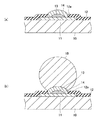
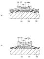
図5は本実施形態に係る半導体装置のバンプ部分の模式断面図である。
実質的に第1実施形態の半導体装置と同様であるが、下地層14aの基板(保護膜12)の表面から突出して形成された部分は、半導体基板10の表面に略平行な平坦な部分を有する上面と半導体基板10の表面に略垂直な外周面とを有している形状であることが異なる。
これは、凸状層13aの形状が半導体基板10の表面に略平行な平坦な部分を有する上面と半導体基板10の表面に略垂直な外周面とを有している形状となっており、この表面形状を反映するように、下地層14aが形成されていることによる。
Second Embodiment FIG. 5 is a schematic cross-sectional view of a bump portion of a semiconductor device according to this embodiment.
Although it is substantially the same as the semiconductor device of the first embodiment, a portion of the
This is a shape in which the shape of the
本実施形態の半導体装置も、第1実施形態と同様に、ハンダバンプの強度が高められており、熱ストレスなどによりクラックが入るのを抑制できる。 Similarly to the first embodiment, the strength of the solder bump is also increased in the semiconductor device of this embodiment, and cracks due to thermal stress can be suppressed.
上記の本実施形態に係る半導体装置のハンダバンプは、以下の効果を享受できる。
(1)基板から突出した下地層を有することにより、下地層とハンダバンプの界面とのせん断応力を大きくでき、接合強度を上げることができる。
(2)下地層の頂部や側面などでハンダバンプと接合することにより、接着強度を上げることができる。
(3)ハンダバンプのネックが括れた形状になることがなく、高い接合信頼性を得ることができる。
(4)実装基板との高い接続信頼性を得ることができる。
(5)逆スパッタリング法によるシードメタル形成工程及び絶縁層形成工程を削除することができ、工程の短縮とコストダウンが実現できる。
The solder bump of the semiconductor device according to the above-described embodiment can enjoy the following effects.
(1) By having the base layer protruding from the substrate, the shear stress between the base layer and the solder bump interface can be increased, and the bonding strength can be increased.
(2) Adhesive strength can be increased by bonding with solder bumps at the top or side surface of the underlayer.
(3) The solder bump neck is not constricted and high bonding reliability can be obtained.
(4) High connection reliability with the mounting substrate can be obtained.
(5) The seed metal formation process and the insulating layer formation process by the reverse sputtering method can be eliminated, and the process can be shortened and the cost can be reduced.
本発明は上記の説明に限定されない。
例えば、バンプの下地層は、上記の層構成に限らず、Ni層以外の層などが積層した構成としてもよい。また下地層の表面形状に反映される凸状層は、所望の形状に形成できる限り、Agナノペースト以外の材料を用いてもよい。
その他、本発明の要旨を逸脱しない範囲で、種々の変更が可能である。
The present invention is not limited to the above description.
For example, the base layer of the bump is not limited to the above layer configuration, and may be a configuration in which layers other than the Ni layer are stacked. Moreover, as long as the convex layer reflected in the surface shape of a base layer can be formed in a desired shape, you may use materials other than Ag nano paste.
In addition, various modifications can be made without departing from the scope of the present invention.
本発明の半導体装置は、フリップチップ実装ができるようにバンプを有する半導体装置に適用できる。
また、本発明の半導体装置の製造方法は、フリップチップ実装ができるようにバンプを有する半導体装置を製造するのに適用できる。
The semiconductor device of the present invention can be applied to a semiconductor device having bumps so that flip chip mounting is possible.
The method for manufacturing a semiconductor device of the present invention can be applied to manufacturing a semiconductor device having bumps so that flip chip mounting is possible.
10…半導体基板、11…パッド電極、12…保護膜、12a…開口部、13,13a…凸状層、14,14a…下地層、15…バンプ、20…実装基板本体、21…配線、22…電極、100…半導体基板、101…パッド電極、102…保護膜、102a…開口部、103…Ti層、104,104a…Cu層、105…マスク層、106…Ni層、107…Au層、108…絶縁樹脂層、109…バンプ
DESCRIPTION OF
Claims (10)
前記電子回路に電気的に接続され、前記半導体基板の表面から突出して形成された下地層と、
前記下地層の前記基板の表面から突出して形成された部分の表面に接合して形成されたハンダからなるバンプと
を有する半導体装置。 A semiconductor substrate on which an electronic circuit is formed;
An underlying layer electrically connected to the electronic circuit and protruding from the surface of the semiconductor substrate;
And a bump made of solder formed by bonding to a surface of a portion of the base layer protruding from the surface of the substrate.
請求項1に記載の半導体装置。 The semiconductor device according to claim 1, wherein a convex layer serving as a mold of a surface shape of the base layer is formed below the base layer.
請求項1に記載の半導体装置。 The semiconductor device according to claim 1, wherein a portion of the base layer that protrudes from the surface of the substrate has a curved surface that smoothly connects from a top portion to an outer peripheral portion.
請求項1に記載の半導体装置。 The portion of the base layer that protrudes from the surface of the substrate has an upper surface having a flat portion that is substantially parallel to the surface of the semiconductor substrate and an outer peripheral surface that is substantially perpendicular to the surface of the semiconductor substrate. A semiconductor device according to 1.
前記半導体基板上に前記パッド電極の一部を開口するパターンの保護膜が形成されており、
前記下地層は前記保護膜の表面から突出して形成されている
請求項1に記載の半導体装置。 A pad electrode electrically connected to the electronic circuit is formed on the semiconductor substrate;
A protective film having a pattern that opens a part of the pad electrode is formed on the semiconductor substrate,
The semiconductor device according to claim 1, wherein the base layer is formed to protrude from a surface of the protective film.
前記下地層の前記基板の表面から突出して形成された部分の表面に接合して、ハンダからなるバンプを形成する工程と
を有する半導体装置の製造方法。 Forming a base layer on the semiconductor substrate on which the electronic circuit is formed, electrically connected to the electronic circuit and protruding from the surface of the semiconductor substrate;
Bonding to the surface of a portion of the base layer protruding from the surface of the substrate to form a bump made of solder.
前記下地層を形成する工程において、前記凸状層の上層に前記凸状層の表面形状が前記下地層の表面形状に反映されるようにして、前記下地層を形成する
請求項6に記載の半導体装置の製造方法。 Before the step of forming the underlayer, the substrate further includes a step of forming a convex layer serving as a mold of the surface shape of the underlayer on the substrate,
The step of forming the underlayer, wherein the underlayer is formed such that the surface shape of the convex layer is reflected on the surface shape of the underlayer on the upper layer of the convex layer. A method for manufacturing a semiconductor device.
請求項6に記載の半導体装置の製造方法。 The step of forming the base layer is formed so that a portion of the base layer that protrudes from the surface of the substrate has a curved surface that smoothly connects from the top to the outer periphery. Semiconductor device manufacturing method.
請求項6に記載の半導体装置の製造方法。 In the step of forming the underlayer, a portion of the underlayer that protrudes from the surface of the substrate has an upper surface having a flat portion that is substantially parallel to the surface of the semiconductor substrate and a surface that is substantially perpendicular to the surface of the semiconductor substrate. The method for manufacturing a semiconductor device according to claim 6, wherein the semiconductor device is formed so as to have a shape having an outer peripheral surface.
前記下地層を形成する工程において、前記保護膜の表面から突出して前記下地層を形成する
請求項6記載の半導体装置の製造方法。 Before the step of forming the base layer, a step of forming a pad electrode by electrically connecting to the electronic circuit on the semiconductor substrate, and a pattern protection for opening a part of the pad electrode on the semiconductor substrate And further forming a film,
The method for manufacturing a semiconductor device according to claim 6, wherein in the step of forming the base layer, the base layer is formed so as to protrude from a surface of the protective film.
Priority Applications (1)
| Application Number | Priority Date | Filing Date | Title |
|---|---|---|---|
| JP2005328652A JP2007134635A (en) | 2005-11-14 | 2005-11-14 | Semiconductor device and manufacturing method thereof |
Applications Claiming Priority (1)
| Application Number | Priority Date | Filing Date | Title |
|---|---|---|---|
| JP2005328652A JP2007134635A (en) | 2005-11-14 | 2005-11-14 | Semiconductor device and manufacturing method thereof |
Publications (1)
| Publication Number | Publication Date |
|---|---|
| JP2007134635A true JP2007134635A (en) | 2007-05-31 |
Family
ID=38156016
Family Applications (1)
| Application Number | Title | Priority Date | Filing Date |
|---|---|---|---|
| JP2005328652A Pending JP2007134635A (en) | 2005-11-14 | 2005-11-14 | Semiconductor device and manufacturing method thereof |
Country Status (1)
| Country | Link |
|---|---|
| JP (1) | JP2007134635A (en) |
Cited By (1)
| Publication number | Priority date | Publication date | Assignee | Title |
|---|---|---|---|---|
| WO2017098809A1 (en) * | 2015-12-11 | 2017-06-15 | 株式会社村田製作所 | Acoustic wave device |
-
2005
- 2005-11-14 JP JP2005328652A patent/JP2007134635A/en active Pending
Cited By (2)
| Publication number | Priority date | Publication date | Assignee | Title |
|---|---|---|---|---|
| WO2017098809A1 (en) * | 2015-12-11 | 2017-06-15 | 株式会社村田製作所 | Acoustic wave device |
| US11444596B2 (en) | 2015-12-11 | 2022-09-13 | Murata Manufacturing Co., Ltd. | Acoustic wave device |
Similar Documents
| Publication | Publication Date | Title |
|---|---|---|
| US7056818B2 (en) | Semiconductor device with under bump metallurgy and method for fabricating the same | |
| JP5764256B2 (en) | Semiconductor chip having support terminal pads | |
| US20150228594A1 (en) | Via under the interconnect structures for semiconductor devices | |
| CN102201351A (en) | Semiconductor device and method for forming dual UBM structure for lead free bump connection | |
| TW200828564A (en) | Multi-chip package structure and method of forming the same | |
| TWI253697B (en) | Method for fabricating a flip chip package | |
| US20060214296A1 (en) | Semiconductor device and semiconductor-device manufacturing method | |
| US20130256871A1 (en) | Semiconductor chip device with fragmented solder structure pads | |
| US20120326299A1 (en) | Semiconductor chip with dual polymer film interconnect structures | |
| US7906424B2 (en) | Conductor bump method and apparatus | |
| US10199345B2 (en) | Method of fabricating substrate structure | |
| JP2010161419A (en) | Method of manufacturing semiconductor device | |
| CN103811442B (en) | Manufacturing method of substrate connection structure | |
| TWI223425B (en) | Method for mounting passive component on wafer | |
| US6956293B2 (en) | Semiconductor device | |
| JP2000164617A (en) | Chip size package and manufacturing method thereof | |
| CN100390982C (en) | Semiconductor device and method for manufacturing semiconductor device | |
| TWI380425B (en) | Fine pitch bump structure and its manufacturing process | |
| JP4631223B2 (en) | Semiconductor package and semiconductor device using the same | |
| JP2007134635A (en) | Semiconductor device and manufacturing method thereof | |
| JP2010092974A (en) | Semiconductor device and method of manufacturing the same, and electronic device | |
| JP5776174B2 (en) | Manufacturing method of electronic component built-in substrate | |
| JP2010157544A (en) | Semiconductor device, method of manufacturing the same, and electronic apparatus | |
| CN100452329C (en) | Semiconductor package substrate for forming pre-solder material and manufacturing method thereof | |
| TWI635546B (en) | Semiconductor structure and method of manufacturing same |