JP2007123725A - CIS thin film solar cell module and method for manufacturing the same - Google Patents
CIS thin film solar cell module and method for manufacturing the same Download PDFInfo
- Publication number
- JP2007123725A JP2007123725A JP2005316846A JP2005316846A JP2007123725A JP 2007123725 A JP2007123725 A JP 2007123725A JP 2005316846 A JP2005316846 A JP 2005316846A JP 2005316846 A JP2005316846 A JP 2005316846A JP 2007123725 A JP2007123725 A JP 2007123725A
- Authority
- JP
- Japan
- Prior art keywords
- solar cell
- cis
- film solar
- thin film
- cell module
- Prior art date
- Legal status (The legal status is an assumption and is not a legal conclusion. Google has not performed a legal analysis and makes no representation as to the accuracy of the status listed.)
- Granted
Links
Images
Classifications
-
- H—ELECTRICITY
- H10—SEMICONDUCTOR DEVICES; ELECTRIC SOLID-STATE DEVICES NOT OTHERWISE PROVIDED FOR
- H10F—INORGANIC SEMICONDUCTOR DEVICES SENSITIVE TO INFRARED RADIATION, LIGHT, ELECTROMAGNETIC RADIATION OF SHORTER WAVELENGTH OR CORPUSCULAR RADIATION
- H10F19/00—Integrated devices, or assemblies of multiple devices, comprising at least one photovoltaic cell covered by group H10F10/00, e.g. photovoltaic modules
- H10F19/30—Integrated devices, or assemblies of multiple devices, comprising at least one photovoltaic cell covered by group H10F10/00, e.g. photovoltaic modules comprising thin-film photovoltaic cells
- H10F19/31—Integrated devices, or assemblies of multiple devices, comprising at least one photovoltaic cell covered by group H10F10/00, e.g. photovoltaic modules comprising thin-film photovoltaic cells having multiple laterally adjacent thin-film photovoltaic cells deposited on the same substrate
-
- H—ELECTRICITY
- H10—SEMICONDUCTOR DEVICES; ELECTRIC SOLID-STATE DEVICES NOT OTHERWISE PROVIDED FOR
- H10F—INORGANIC SEMICONDUCTOR DEVICES SENSITIVE TO INFRARED RADIATION, LIGHT, ELECTROMAGNETIC RADIATION OF SHORTER WAVELENGTH OR CORPUSCULAR RADIATION
- H10F10/00—Individual photovoltaic cells, e.g. solar cells
- H10F10/10—Individual photovoltaic cells, e.g. solar cells having potential barriers
- H10F10/16—Photovoltaic cells having only PN heterojunction potential barriers
- H10F10/167—Photovoltaic cells having only PN heterojunction potential barriers comprising Group I-III-VI materials, e.g. CdS/CuInSe2 [CIS] heterojunction photovoltaic cells
-
- H—ELECTRICITY
- H02—GENERATION; CONVERSION OR DISTRIBUTION OF ELECTRIC POWER
- H02S—GENERATION OF ELECTRIC POWER BY CONVERSION OF INFRARED RADIATION, VISIBLE LIGHT OR ULTRAVIOLET LIGHT, e.g. USING PHOTOVOLTAIC [PV] MODULES
- H02S40/00—Components or accessories in combination with PV modules, not provided for in groups H02S10/00 - H02S30/00
- H02S40/30—Electrical components
- H02S40/38—Energy storage means, e.g. batteries, structurally associated with PV modules
-
- H—ELECTRICITY
- H10—SEMICONDUCTOR DEVICES; ELECTRIC SOLID-STATE DEVICES NOT OTHERWISE PROVIDED FOR
- H10F—INORGANIC SEMICONDUCTOR DEVICES SENSITIVE TO INFRARED RADIATION, LIGHT, ELECTROMAGNETIC RADIATION OF SHORTER WAVELENGTH OR CORPUSCULAR RADIATION
- H10F19/00—Integrated devices, or assemblies of multiple devices, comprising at least one photovoltaic cell covered by group H10F10/00, e.g. photovoltaic modules
- H10F19/80—Encapsulations or containers for integrated devices, or assemblies of multiple devices, having photovoltaic cells
-
- H—ELECTRICITY
- H10—SEMICONDUCTOR DEVICES; ELECTRIC SOLID-STATE DEVICES NOT OTHERWISE PROVIDED FOR
- H10F—INORGANIC SEMICONDUCTOR DEVICES SENSITIVE TO INFRARED RADIATION, LIGHT, ELECTROMAGNETIC RADIATION OF SHORTER WAVELENGTH OR CORPUSCULAR RADIATION
- H10F71/00—Manufacture or treatment of devices covered by this subclass
-
- Y—GENERAL TAGGING OF NEW TECHNOLOGICAL DEVELOPMENTS; GENERAL TAGGING OF CROSS-SECTIONAL TECHNOLOGIES SPANNING OVER SEVERAL SECTIONS OF THE IPC; TECHNICAL SUBJECTS COVERED BY FORMER USPC CROSS-REFERENCE ART COLLECTIONS [XRACs] AND DIGESTS
- Y02—TECHNOLOGIES OR APPLICATIONS FOR MITIGATION OR ADAPTATION AGAINST CLIMATE CHANGE
- Y02E—REDUCTION OF GREENHOUSE GAS [GHG] EMISSIONS, RELATED TO ENERGY GENERATION, TRANSMISSION OR DISTRIBUTION
- Y02E10/00—Energy generation through renewable energy sources
- Y02E10/50—Photovoltaic [PV] energy
- Y02E10/541—CuInSe2 material PV cells
-
- Y—GENERAL TAGGING OF NEW TECHNOLOGICAL DEVELOPMENTS; GENERAL TAGGING OF CROSS-SECTIONAL TECHNOLOGIES SPANNING OVER SEVERAL SECTIONS OF THE IPC; TECHNICAL SUBJECTS COVERED BY FORMER USPC CROSS-REFERENCE ART COLLECTIONS [XRACs] AND DIGESTS
- Y02—TECHNOLOGIES OR APPLICATIONS FOR MITIGATION OR ADAPTATION AGAINST CLIMATE CHANGE
- Y02E—REDUCTION OF GREENHOUSE GAS [GHG] EMISSIONS, RELATED TO ENERGY GENERATION, TRANSMISSION OR DISTRIBUTION
- Y02E70/00—Other energy conversion or management systems reducing GHG emissions
- Y02E70/30—Systems combining energy storage with energy generation of non-fossil origin
-
- Y—GENERAL TAGGING OF NEW TECHNOLOGICAL DEVELOPMENTS; GENERAL TAGGING OF CROSS-SECTIONAL TECHNOLOGIES SPANNING OVER SEVERAL SECTIONS OF THE IPC; TECHNICAL SUBJECTS COVERED BY FORMER USPC CROSS-REFERENCE ART COLLECTIONS [XRACs] AND DIGESTS
- Y02—TECHNOLOGIES OR APPLICATIONS FOR MITIGATION OR ADAPTATION AGAINST CLIMATE CHANGE
- Y02P—CLIMATE CHANGE MITIGATION TECHNOLOGIES IN THE PRODUCTION OR PROCESSING OF GOODS
- Y02P70/00—Climate change mitigation technologies in the production process for final industrial or consumer products
- Y02P70/50—Manufacturing or production processes characterised by the final manufactured product
Landscapes
- Photovoltaic Devices (AREA)
Abstract
【課題】低コストで、長期の耐久性を有する太陽電池モジュールを得る。
【解決手段】CIS系薄膜太陽電池モジュール1は、ガラス基板2A上に形成されたCIS系薄膜太陽電池サーキット2に、加熱して架橋したエチレンビニルアセテート(以下、EVAという。)樹脂フィルム3(又はシート)を接着剤として、安価で耐久性のある白板半強化ガラス等からなるカバーガラス4を貼着する。EVA樹脂フィルム3を使用することにより、EVA樹脂の使用量を削減する。前記架橋する際に真空吸引してEVA樹脂フィルムから発生するガス分を吸引し、泡等の発生を防止する。ガラス基板のサーキット設置面と反対面に、大容量の蓄電キャパシタ9を設け、その光発電電力を蓄電する。
【選択図】図1A solar cell module having long-term durability at low cost is obtained.
A CIS-based thin film solar cell module 1 is an ethylene vinyl acetate (hereinafter referred to as EVA) resin film 3 (or EVA) that is heated and cross-linked to a CIS-based thin film solar cell circuit 2 formed on a glass substrate 2A. A cover glass 4 made of white plate semi-tempered glass and the like, which is inexpensive and durable, is attached using a sheet) as an adhesive. By using the EVA resin film 3, the amount of EVA resin used is reduced. When the cross-linking is performed, vacuum suction is performed to suck a gas component generated from the EVA resin film, thereby preventing generation of bubbles and the like. A large-capacity storage capacitor 9 is provided on the surface of the glass substrate opposite to the circuit installation surface, and the photovoltaic power is stored.
[Selection] Figure 1
Description
本発明は、多元化合物半導体薄膜を光吸収層として使用したヘテロ接合薄膜太陽電池デバイスから構成されるCIS系薄膜太陽電池モジュール、その製造方法及び該モジュールの設置方法に関する。 The present invention relates to a CIS-based thin-film solar cell module composed of a heterojunction thin-film solar cell device using a multi-component compound semiconductor thin film as a light absorption layer, a manufacturing method thereof, and a method for installing the module.
CIS系薄膜太陽電池モジュールは、近年、広範囲に実用化が可能であるとみなされ、米国、ドイツ等で商業化され、日本でも精力的に高性能化と製造技術の開発が進められている。これまでの研究開発では、モジュールの長期の耐久性に関する作製例、環境試験による評価例として、CIS系薄膜太陽電池モジュールは薄型、省資源、大面積で大量生産可能である特徴を有するが、その耐久性に関する研究例は少ない。一方、Si結晶系の太陽電池モジュールにおいて、耐久性を維持するため、複数のSi結晶系太陽電池セルをリボン導線等により電気的に接続した太陽電池アレイを、2枚のガラス板等の透光性を有する板で挟み、この太陽電池アレイを架橋したEVA樹脂中に埋め込むか又は架橋したEVA樹脂で封入する方法(又は構造)(例えば、特許文献1参照。)が採用されていた。しかし、前記Si結晶系の太陽電池モジュールの場合は、光入射側のカバーガラスの他に太陽電池アレイを挟持するためのガラス板を必要とする(CIS系薄膜太陽電池モジュールはガラス基板上に太陽電池モジュールが形成されるので、ガラス板はカバーガラス1枚で済む。)ため、透光性を有するガラス板の使用枚数が増加すると共に、高価なEVA樹脂を多量に使用するため、コスト増加の要因となっていた。CIS系薄膜太陽電池モジュールは比較的機械的強度の高いガラス基板上に複数の太陽電池デバイスが形成されているという、前記Si結晶系の太陽電池モジュールとその基本構造が異なり、CIS系薄膜太陽電池モジュールに適合した耐久構造が求められている。 In recent years, CIS-based thin-film solar cell modules are considered to be practically used in a wide range, and are commercialized in the United States, Germany, and the like. In R & D so far, CIS-based thin-film solar cell modules have features that are thin, resource-saving, and can be mass-produced in large areas, as examples of making long-term durability of modules and evaluation examples of environmental tests. There are few studies on durability. On the other hand, in order to maintain durability in a Si crystal solar cell module, a solar cell array in which a plurality of Si crystal solar cells are electrically connected by a ribbon conductor or the like is used to transmit light such as two glass plates. A method (or structure) (for example, see Patent Document 1) in which the solar cell array is embedded in a cross-linked EVA resin or sealed with a cross-linked EVA resin is employed. However, in the case of the Si crystal solar cell module, in addition to the cover glass on the light incident side, a glass plate for sandwiching the solar cell array is required (the CIS thin film solar cell module has a solar cell on a glass substrate). Since the battery module is formed, only one cover glass is required for the glass plate.) Therefore, the number of translucent glass plates used is increased, and a large amount of expensive EVA resin is used. It was a factor. The CIS thin film solar cell module is different from the Si crystal solar cell module in which a plurality of solar cell devices are formed on a glass substrate having a relatively high mechanical strength, and the basic structure thereof is different. A durable structure suitable for the module is required.
また、CIS系薄膜太陽電池モジュールは薄型、省資源、大面積という特徴を有するが、CIS系薄膜太陽電池モジュールで発電された電力はモジュール外に設けた鉛蓄電池、ニッケル水素電池、ニッカド電池、リチウム電池等の二次電池に蓄電して使用又は売電されているが、これら二次電池はその蓄電容量、重量及び体積等に問題があり、太陽電池モジュールと一体構造にすることはできなかった。 In addition, the CIS thin film solar cell module has the characteristics of being thin, resource saving, and large area, but the electric power generated by the CIS thin film solar cell module is a lead storage battery, nickel hydride battery, nickel cadmium battery, lithium The secondary battery such as a battery is stored and used or sold, but these secondary batteries have problems with their storage capacity, weight, volume, etc., and could not be integrated with the solar cell module. .
しかし、近年、軽量、薄型で大容量の蓄電素子であるキャパシタ(例えば、特許文献2及び非特許文献1参照。)の研究が進みその様々な用途が考えられている。 However, in recent years, studies on capacitors (see, for example, Patent Document 2 and Non-Patent Document 1) that are light-weight, thin, and large-capacity storage elements have progressed, and various uses thereof have been considered.
そして、太陽電池モジュールと前記蓄電用キャパシタとを一体構造にする試み(例えば、特許文献1、非特許文献1及び非特許文献2参照。)もなされているが、前記太陽電池モジュールがSi結晶系の太陽電池モジュールの場合、CIS系薄膜太陽電池モジュールのように大面積でなく、機械的強度の高いガラス基板を使用していないため、太陽電池モジュールと蓄電用キャパシタとを一体構造にするには、機械的強度を維持するための機構部材を別途設ける必要があり、重量、体積及びコストが増大するという問題がある。 An attempt has been made to integrate the solar cell module and the storage capacitor (see, for example, Patent Document 1, Non-Patent Document 1, and Non-Patent Document 2). In the case of the solar cell module, since the glass substrate having a large area and not high mechanical strength is used unlike the CIS-based thin film solar cell module, the solar cell module and the storage capacitor are integrated. Further, it is necessary to separately provide a mechanism member for maintaining the mechanical strength, and there is a problem that the weight, volume and cost increase.
本発明は前記のような問題点を解消するもので、本発明の目的は、低コストで屋外環境での使用に耐える長期の耐久性を有するCIS系薄膜太陽電池モジュールを得ることである。 The present invention solves the above-mentioned problems, and an object of the present invention is to obtain a CIS-based thin-film solar cell module having long-term durability that can withstand use in an outdoor environment at low cost.
本発明は前記のような問題点を解消するもので、本発明の目的は、真空脱気後、EVA樹脂フィルムを加熱溶融拡散させた後に、大気圧でEVA樹脂フィルムを架橋することにより、CIS系薄膜太陽電池サーキット中の泡の発生を防止する。 The present invention solves the above-mentioned problems, and the object of the present invention is to provide a CIS by cross-linking an EVA resin film at atmospheric pressure after heating and diffusing the EVA resin film after vacuum degassing. Generation of bubbles in the thin film solar cell circuit.
本発明のその他の目的は、高価なバックシートの使用量を削減して、コストを削減することである。 Another object of the present invention is to reduce the cost by reducing the amount of expensive backsheet used.
更に、本発明のその他の目的は、前記CIS系薄膜太陽電池モジュールのCIS系薄膜太陽電池デバイス部のガラス基板の裏面(太陽光入射面と反対面)に薄型、軽量で且つ大容量の蓄電デバイスである蓄電キャパシタを設けることにより、低コストで長期の耐久性を有すると共に、小型、軽量で且つ大容量の蓄電能力を有するCIS系薄膜太陽電池モジュールを得ることである。 Furthermore, another object of the present invention is to provide a thin, lightweight and large-capacity electricity storage device on the back surface (the surface opposite to the sunlight incident surface) of the glass substrate of the CIS thin film solar cell device portion of the CIS thin film solar cell module. It is to obtain a CIS-based thin film solar cell module having long-term durability at a low cost and having a small, lightweight and large-capacity storage capacity by providing the storage capacitor.
更に、本発明のその他の目的は、低コストで長期の耐久性を有すると共に、前記蓄電能力を有するCIS系薄膜太陽電池モジュールにより、廉価の夜間電力を蓄電キャパシタに蓄電し、昼間の太陽光発電電力を使用又は売電することにより、CIS系薄膜太陽電池モジュールの設置又は使用コストを低減することである。 Furthermore, another object of the present invention is to store low-cost nighttime power in a storage capacitor with a CIS-based thin film solar cell module having low-cost and long-term durability and having the above-mentioned storage capability, and daytime solar power generation It is to reduce the installation or use cost of the CIS-based thin film solar cell module by using or selling power.
(1)本発明は、ガラス基板上に、アルカリバリア層、金属裏面電極層、光吸収層、バッファ層、窓層の順に積層された複数のCIS系薄膜太陽電池デバイス部が導電パターンにより電気的に接続されたCIS系薄膜太陽電池サーキット(又はサブモジュール)に、加熱して重合反応を起こさせて架橋したエチレンビニルアセテート(以下、EVAという。)樹脂フィルム(又はシート)を接着剤として、白板半強化ガラス等からなるカバーガラスを貼着した構造からなるCIS系薄膜太陽電池モジュールである。 (1) In the present invention, a plurality of CIS-based thin-film solar cell device portions laminated in the order of an alkali barrier layer, a metal back electrode layer, a light absorption layer, a buffer layer, and a window layer on a glass substrate are electrically connected by a conductive pattern. A CIS-based thin film solar cell circuit (or submodule) connected to a white plate with an ethylene vinyl acetate (hereinafter referred to as EVA) resin film (or sheet) crosslinked by heating to cause a polymerization reaction as an adhesive. It is a CIS thin film solar cell module having a structure in which a cover glass made of semi-tempered glass or the like is attached.
(2)本発明は、前記CIS系薄膜太陽電池サーキット(又はサブモジュール)のガラス基板の光入射面と反対面(太陽電池サーキット設置面と反対面)の外周部にバックシートを貼着した構造からなる前記(1)に記載のCIS系薄膜太陽電池モジュールである。 (2) The present invention has a structure in which a back sheet is adhered to the outer peripheral portion of the surface opposite to the light incident surface (the surface opposite to the solar cell circuit installation surface) of the glass substrate of the CIS thin film solar cell circuit (or submodule). The CIS-based thin-film solar cell module according to (1) above.
(3)本発明は、前記ガラス基板の所定箇所にCIS系薄膜太陽電池サーキット面からその反対側の面に貫通する穴を設け、その内壁に導電膜を形成し、前記導電膜はCIS系薄膜太陽電池サーキットとその反対側の面に設置される電子部品と接続する前記(1)又は(2)に記載のCIS系薄膜太陽電池モジュールである。 (3) In the present invention, a hole penetrating from the CIS-based thin film solar cell circuit surface to the opposite surface is provided at a predetermined location of the glass substrate, and a conductive film is formed on the inner wall thereof. The CIS-based thin-film solar cell module according to (1) or (2), which is connected to a solar cell circuit and an electronic component installed on the opposite surface.
(4)本発明は、前記ガラス基板のCIS系薄膜太陽電池サーキット設置面と反対面に、大容量の蓄電キャパシタを設けた前記(1)、(2)又は(3)に記載のCIS系薄膜太陽電池モジュールである。 (4) The present invention provides the CIS thin film according to (1), (2) or (3), wherein a large-capacity storage capacitor is provided on the surface of the glass substrate opposite to the CIS thin film solar cell circuit installation surface. It is a solar cell module.
(5)本発明は、前記蓄電キャパシタが、昼間に前記CIS系薄膜太陽電池サーキットの光発電電力を蓄電し、夜間に廉価な夜間電力を蓄電する前記(3)に記載のCIS系薄膜太陽電池モジュールである。 (5) The present invention provides the CIS thin film solar cell according to (3), wherein the storage capacitor stores photovoltaic power generated by the CIS thin film solar cell circuit in the daytime and stores inexpensive nighttime power at night. It is a module.
(6)本発明は、ガラス基板上に、アルカリバリア層、金属裏面電極層、光吸収層、バッファ層、窓層の順に積層された複数のCIS系薄膜太陽電池デバイス部が導電パターンにより電気的に接続されたCIS系薄膜太陽電池サーキット(又はサブモジュール)に、加熱して重合反応を起こさせて架橋し、接着剤として作用するエチレンビニルアセテート(以下、EVAという。)樹脂フィルム(又はシート)を介して、白板半強化ガラス等からなるカバーガラスを貼着するCIS系薄膜太陽電池モジュールの製造方法である。 (6) In the present invention, a plurality of CIS-based thin-film solar cell device parts laminated in the order of an alkali barrier layer, a metal back electrode layer, a light absorption layer, a buffer layer, and a window layer on a glass substrate are electrically connected by a conductive pattern. An ethylene vinyl acetate (hereinafter referred to as EVA) resin film (or sheet) that acts as an adhesive by crosslinking a CIS-based thin-film solar cell circuit (or submodule) connected to a polymer by heating to cause a polymerization reaction. It is a manufacturing method of the CIS type thin film solar cell module which sticks the cover glass which consists of white board semi-tempered glass etc. through.
(7)本発明は、前記EVA樹脂フィルム(又はシート)を架橋する際に発生するガス分を真空吸引して、泡等の発生を防止する前記(6)に記載のCIS系薄膜太陽電池モジュールの製造方法である。 (7) The present invention provides a CIS-based thin-film solar cell module according to (6), wherein the gas generated when the EVA resin film (or sheet) is crosslinked is vacuum-sucked to prevent generation of bubbles and the like. It is a manufacturing method.
(8)本発明は、前記CIS系薄膜太陽電池サーキット上にガラス基板と同サイズのEVA樹脂フィルム(又はシート)を載せ、四隅に短冊状に切ったEVA樹脂フィルム(又はシート)を載せ、その上にカバーガラスを載せ、このCIS系薄膜太陽電池サーキットとカバーガラスの間に前記EVA樹脂フィルム(又はシート)が挟持された構造体を真空加熱装置に入れ、真空脱気しつつ、80〜120℃まで加熱(ホットプレート)して前記EVA樹脂シートをガラス全面に溶融拡散させた後、徐々に大気に戻し加圧した後、140℃〜150℃の温度で加熱(ホットプレート)して前記EVA樹脂フィルム(又はシート)を架橋する前記(6)及び(7)に記載のCIS系薄膜太陽電池モジュールの製造方法である。 (8) In the present invention, an EVA resin film (or sheet) of the same size as the glass substrate is placed on the CIS thin film solar cell circuit, and an EVA resin film (or sheet) cut into strips is placed at the four corners. A cover glass is placed on top, and the structure in which the EVA resin film (or sheet) is sandwiched between the CIS-based thin film solar cell circuit and the cover glass is placed in a vacuum heating device, and vacuum degassed. The EVA resin sheet is melted and diffused over the entire surface of the glass by heating up to ° C (hot plate), then gradually returned to the atmosphere and pressurized, and then heated (hot plate) at a temperature of 140 ° C to 150 ° C. It is a manufacturing method of the CIS type thin film solar cell module as described in said (6) and (7) which bridge | crosslinks a resin film (or sheet | seat).
本発明は、加熱により重合反応させて架橋させることにより、EVA樹脂フィルム(又はシート)を接着剤として使用し、前記架橋したEVA樹脂フィルムを介してCIS系薄膜太陽電池デバイス部(サーキット又はサブモジュール)に、白板半強化ガラス等からなるカバーガラスを貼着することにより、低コストで屋外環境での使用に耐える長期の耐久性を有するCIS系薄膜太陽電池モジュールを得ることができる。 In the present invention, an EVA resin film (or sheet) is used as an adhesive by causing a polymerization reaction by crosslinking by heating, and a CIS-based thin film solar cell device portion (circuit or submodule) is passed through the crosslinked EVA resin film. ), A CIS-based thin film solar cell module having a long-term durability that can withstand use in an outdoor environment can be obtained at a low cost.
本発明は、EVA樹脂フィルムを架橋する際、真空脱気しつつ、加熱することにより、CIS系薄膜太陽電池サーキット中の泡の発生を防止することができる。 In the present invention, when the EVA resin film is cross-linked, it is possible to prevent generation of bubbles in the CIS-based thin film solar cell circuit by heating while vacuum degassing.
本発明は、前記CIS系薄膜太陽電池モジュールのCIS系薄膜太陽電池デバイス部のガラス基板の裏面(太陽光入射面と反対面)に設ける高価なバックシートをモジュールの一部(周辺部)に設けることにより、バックシートの使用量を削減して、低コストで長期の耐久性を有するCIS系薄膜太陽電池モジュールを得ることができる。 In the present invention, an expensive back sheet provided on the back surface (the surface opposite to the sunlight incident surface) of the CIS-based thin-film solar cell device portion of the CIS-based thin-film solar cell module is provided on a part (peripheral portion) of the module. Thereby, the usage-amount of a back sheet can be reduced, and the CIS type thin film solar cell module which has long-term durability at low cost can be obtained.
更に、本発明は、低コストで長期の耐久性を有すると共に、前記CIS系薄膜太陽電池モジュールのCIS系薄膜太陽電池デバイス部のガラス基板の裏面(太陽光入射面と反対面)に、近年開発且つ製品化されている薄型、軽量で且つ大容量の蓄電デバイスである蓄電キャパシタを設けることにより、小型、軽量で且つ大容量の蓄電能力を有するCIS系薄膜太陽電池モジュールを得ることができる。 Furthermore, the present invention has recently been developed on the back surface (the surface opposite to the sunlight incident surface) of the glass substrate of the CIS-based thin-film solar cell device portion of the CIS-based thin-film solar cell module, while having low cost and long-term durability. In addition, by providing a storage capacitor that is a thin, lightweight, and large-capacity storage device that has been commercialized, a CIS-based thin-film solar cell module that has a small, lightweight, and large-capacity storage capability can be obtained.
更に、本発明は、低コストで長期の耐久性を有すると共に、前記蓄電能力を有するCIS系薄膜太陽電池モジュールを設けることにより、廉価の夜間電力を蓄電キャパシタに蓄電し、昼間の太陽光発電電力を使用又は売電することにより、CIS系薄膜太陽電池モジュールの設置又は使用コストを低減することができる。 Furthermore, the present invention provides a CIS-based thin-film solar cell module having low cost and long-term durability and having the above-mentioned storage capability, thereby storing inexpensive nighttime power in a storage capacitor, and daytime photovoltaic power generation By using or selling power, the installation or use cost of the CIS thin film solar cell module can be reduced.
本発明は、CIS系薄膜太陽電池モジュール及びその製造方法に関するものである。CIS系薄膜太陽電池モジュール1は、図1に示す、多元化合物半導体薄膜を光吸収層として使用したヘテロ接合薄膜太陽電池、特に、Cu-III-VI2族カルコパイライト半導体、例えば、二セレン化銅インジウム(CISe)、二セレン化銅インジウム・ガリウム(CIGSe) 、二セレン・イオウ化銅インジウム・ガリウム(CIGSSe)、二イオウ化銅インジウム・ガリウム(CIGS)又は薄膜の二セレン・イオウ化銅インジウム・ガリウム(CIGSSe)層を表面層として有する二セレン化銅インジウム・ガリウム(CIGSe) のようなp形半導体の光吸収層とpnヘテロ接合を有するCIS系薄膜太陽電池サーキット(複数のCIS系薄膜太陽電池デバイス2’がパターンニングにより接続されたサーキット(又はサブモジュール))2からなるCIS系薄膜太陽電池モジュールであり、CIS系薄膜太陽電池モジュール1は、図2に示すように、CIS系薄膜太陽電池サーキット2にカバーガラス4が接着剤としての架橋されたEVA樹脂等のプラスチック樹脂フィルム(又はシート)3により接着された構造体STが形成される。そして、図1に示すように、前記構造体STの裏面に、バックシート5及びケーブル付き接続箱6が設置され、この構造体STの外周部にシール材7を介してフレーム8が取り付けられる。 The present invention relates to a CIS-based thin film solar cell module and a manufacturing method thereof. The CIS-based thin film solar cell module 1 is a heterojunction thin film solar cell using a multi-component compound semiconductor thin film as a light absorption layer, particularly a Cu-III-VI group 2 chalcopyrite semiconductor, such as copper diselenide, as shown in FIG. Indium (CISe), copper indium gallium selenide (CIGSe), copper indium gallium selenide (CIGSSe), copper indium disulfide indium gallium (CIGS) or thin film indium selenium indium disulfide CIS thin film solar cell circuit having a pn heterojunction and a light absorption layer of a p-type semiconductor such as copper indium gallium selenide (CIGSe) having a gallium (CIGSSe) layer as a surface layer (multiple CIS thin film solar cells A device 2 'is a CIS-based thin-film solar cell module comprising a circuit (or submodule) 2 connected by patterning, and C As shown in FIG. 2, the S-based thin-film solar cell module 1 has a cover glass 4 bonded to a CIS-based thin-film solar cell circuit 2 with a plastic resin film (or sheet) 3 such as a crosslinked EVA resin as an adhesive. The structure ST is formed. And as shown in FIG. 1, the back sheet 5 and the connection box 6 with a cable are installed in the back surface of the said structure ST, and the flame | frame 8 is attached to the outer peripheral part of this structure ST via the sealing material 7. As shown in FIG.
また、前記CIS系薄膜太陽電池デバイス部2’は、図3に示すように、ガラス基板2A上に、アルカリバリア層2B、金属裏面電極層2C、p形半導体の光吸収層2D、高抵抗のバッファ層2E、n形の透明導電膜からなる窓層2Fの順に積層された積層構造である。
Further, as shown in FIG. 3, the CIS-based thin film solar cell device portion 2 ′ has an
本発明のCIS系薄膜太陽電池モジュール1の特徴は、ガラス基板2A上に形成したCIS系薄膜太陽電池サーキット2に、加熱して重合反応を起こさせて架橋したエチレンビニルアセテート(以下、EVAという。)樹脂フィルム(又はシート、以下、フィルムという。)3を接着剤として、比較的安価で機械的強度が高く耐久性のある白板半強化ガラス等からなるカバーガラス4を貼着した構造を採っている。前記EVA樹脂フィルム3を使用することにより、EVA樹脂の使用量が削減され製造コストを削減することができる。また、前記カバーガラス4に白板半強化ガラスを使用することにより、耐久性を向上することができる。
A feature of the CIS thin film solar cell module 1 of the present invention is ethylene vinyl acetate (hereinafter referred to as EVA) in which a CIS thin film solar cell circuit 2 formed on a
前記EVA樹脂フィルム3を架橋する際に発生するガス分を真空吸引して、泡等の発生を防止する。 A gas component generated when the EVA resin film 3 is cross-linked is vacuumed to prevent generation of bubbles and the like.
前記CIS系薄膜太陽電池サーキット2にカバーガラス4が接着剤としての架橋されたEVA樹脂等のプラスチック樹脂フィルム3により接着された構造体STの製造方法の詳細を以下に示す。
前記CIS系薄膜太陽電池サーキット2上にガラス基板2Aと同サイズのEVA樹脂フィルム3を載せ、更に、四隅に短冊状に切ったEVA樹脂フィルム3A(図示省略)を載せ、その上にカバーガラス4を載せ、このCIS系薄膜太陽電池サーキット2とカバーガラス4の間に前記EVA樹脂フィルム3及び3Aが挟持された構造体STを真空加熱装置に入れ、真空脱気しつつ、80〜120℃まで加熱(ホットプレート)して前記EVA樹脂フィルムをガラス全面に溶融拡散させた後、徐々に大気に戻し加圧した後、140℃〜150℃の温度で加熱(ホットプレート)して前記EVA樹脂フィルム3及び3Aを架橋する。なお、前記四隅に短冊状に切ったEVA樹脂フィルム3Aを載せる理由は、ガラス基板2Aと同サイズのEVA樹脂フィルム3を載せるだけでは、加圧時に溶融したEVA樹脂が四隅からはみ出して端が薄くなりEVA樹脂層の厚みが一定にならないので、これを補充するたのものである。
Details of the manufacturing method of the structure ST in which the cover glass 4 is bonded to the CIS-based thin film solar cell circuit 2 with a plastic resin film 3 such as a crosslinked EVA resin as an adhesive will be described below.
An EVA resin film 3 having the same size as the
前記方法のように真空脱気しつつ、加熱して溶融拡散することにより、EVA樹脂フィルム3及び3AとCIS系薄膜太陽電池サーキット2との間及びEVA樹脂フィルム3及び3Aとカバーガラス4との間に残存する空気や、加熱によりEVA樹脂フィルム3及び3Aから発生するガスを脱気することにより、前記構造体ST中に前記空気やEVA樹脂フィルム3からの発生ガスによる泡の発生を防止することができ、光の透過率及び美観の低下を防止することができる。また、フイルム状又はシート状のEVA樹脂フィルム3及び3Aを使用するため、EVA樹脂の使用量が削減され、製造コストを低減することができる。 While being vacuum degassed as in the above method, by heating and diffusing, between the EVA resin films 3 and 3A and the CIS thin film solar cell circuit 2 and between the EVA resin films 3 and 3A and the cover glass 4 The generation of bubbles due to the air and gas generated from the EVA resin film 3 in the structure ST is prevented by degassing the air remaining between them and the gas generated from the EVA resin films 3 and 3A by heating. It is possible to prevent a decrease in light transmittance and aesthetics. Moreover, since the film-shaped or sheet-shaped EVA resin films 3 and 3A are used, the amount of the EVA resin used is reduced, and the manufacturing cost can be reduced.
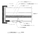
本発明のCIS系薄膜太陽電池モジュール1は、図1に示すように、前記CIS系薄膜太陽電池サーキット2のガラス基板2Aの光入射面と反対面(太陽電池サーキット設置面と反対面)にバックシート5を貼着しているが、図5に示すように、前記バックシート5をCIS系薄膜太陽電池モジュール1の外周部(フレーム8の近傍)に設けることにより、バックシート5の使用量が削減され、製造コストを削減することができる。
As shown in FIG. 1, the CIS thin film solar cell module 1 of the present invention is backed on the surface opposite to the light incident surface (surface opposite to the solar cell circuit installation surface) of the
更に、本発明のCIS系薄膜太陽電池モジュール1の特徴は、予め、前記ガラス基板2Aの所定箇所にCIS系薄膜太陽電池サーキット面からその反対側の面に貫通する穴を設けておき、金属裏面電極層又は導電パターンの形成時に、その内壁に導電膜を形成する。前記導電膜はCIS系薄膜太陽電池サーキット2とその反対側の面に設置される電子部品との接続の際に使用される。
Furthermore, the feature of the CIS thin film solar cell module 1 of the present invention is that a hole penetrating from the CIS thin film solar cell circuit surface to the opposite surface is provided in advance at a predetermined location of the
更に、本発明のCIS系薄膜太陽電池モジュール1の特徴は、図4に示すように、前記ガラス基板2AのCIS系薄膜太陽電池サーキット設置面と反対面に、大容量の蓄電キャパシタ9を設けることである。前記蓄電キャパシタ9はそれが設置されているガラス基板上のCIS系薄膜太陽電池サーキット2の発電能力と同等のものを各モジュール1毎に設置する。また、CIS系薄膜太陽電池サーキット2発電能力以上の蓄電容量を有するものを使用する場合には、その蓄電容量に応じて、図1に示す蓄電キャパシタ9を有しないCIS系薄膜太陽電池モジュール1と組み合わせて設置する。なお、蓄電キャパシタ9を有するCIS系薄膜太陽電池モジュール1は、電力会社からの電力供給口近傍又は屋根面の上端、下端、側端等の周辺部に設置することにより、モジュール1の故障又は交換等の際に都合が良い。
Furthermore, as shown in FIG. 4, the CIS thin film solar cell module 1 of the present invention is characterized in that a large-capacity storage capacitor 9 is provided on the surface opposite to the CIS thin film solar cell circuit installation surface of the
更に、本発明のCIS系薄膜太陽電池モジュール1の特徴は、前記蓄電キャパシタ9を具備するCIS系薄膜太陽電池モジュール1は、昼間に前記CIS系薄膜太陽電池モジュール1の光発電電力を蓄電し、夜間に廉価な夜間電力を蓄電することができ、設置後の維持コストを削減することができる。 Further, the CIS thin film solar cell module 1 of the present invention is characterized in that the CIS thin film solar cell module 1 including the storage capacitor 9 stores the photovoltaic power of the CIS thin film solar cell module 1 in the daytime. Inexpensive nighttime electric power can be stored at night, and maintenance costs after installation can be reduced.
1 CIS系薄膜太陽電池モジュール
2 CIS系薄膜太陽電池サーキット
2’ CIS系薄膜太陽電池デバイス部
2A ガラス基板
2B アルカリバリア層
2C 金属裏面電極層
2D 光吸収層
2E バッファ層
2F 窓層
3 EVA樹脂フィルム(又はシート)
3A 短冊状のEVA樹脂フィルム
4 カバーガラス
5 バックシート
6 ケーブル付き接続箱
7 シール材
8 フレーム
9 蓄電用キャパシタ
ST 構造体
DESCRIPTION OF SYMBOLS 1 CIS type thin film solar cell module 2 CIS type thin film solar cell circuit 2 'CIS type thin film solar
3A Strip-shaped EVA resin film 4 Cover glass 5 Back sheet 6 Connection box with cable 7 Seal material 8 Frame 9 Capacitor for power storage ST structure
Claims (8)
Priority Applications (7)
| Application Number | Priority Date | Filing Date | Title |
|---|---|---|---|
| JP2005316846A JP4918247B2 (en) | 2005-10-31 | 2005-10-31 | CIS thin film solar cell module and method for manufacturing the same |
| US12/092,094 US7960642B2 (en) | 2005-10-31 | 2006-10-31 | CIS based thin-film photovoltaic module and process for producing the same |
| EP06822707.3A EP1947704B1 (en) | 2005-10-31 | 2006-10-31 | Process for producing a cis-type thin-film solar battery module |
| CNA2006800408353A CN101300683A (en) | 2005-10-31 | 2006-10-31 | CIS-based thin film solar cell module and method for manufacturing same |
| PCT/JP2006/321778 WO2007052671A1 (en) | 2005-10-31 | 2006-10-31 | Cis-type thin-film solar battery module and process for producing the same |
| KR1020087010613A KR101275651B1 (en) | 2005-10-31 | 2006-10-31 | CIS-type thin-film solar battery module and process for producing the same |
| TW095140220A TW200729529A (en) | 2005-10-31 | 2006-10-31 | CIS series thin film solar cell module and the making method |
Applications Claiming Priority (1)
| Application Number | Priority Date | Filing Date | Title |
|---|---|---|---|
| JP2005316846A JP4918247B2 (en) | 2005-10-31 | 2005-10-31 | CIS thin film solar cell module and method for manufacturing the same |
Publications (2)
| Publication Number | Publication Date |
|---|---|
| JP2007123725A true JP2007123725A (en) | 2007-05-17 |
| JP4918247B2 JP4918247B2 (en) | 2012-04-18 |
Family
ID=38005824
Family Applications (1)
| Application Number | Title | Priority Date | Filing Date |
|---|---|---|---|
| JP2005316846A Expired - Fee Related JP4918247B2 (en) | 2005-10-31 | 2005-10-31 | CIS thin film solar cell module and method for manufacturing the same |
Country Status (7)
| Country | Link |
|---|---|
| US (1) | US7960642B2 (en) |
| EP (1) | EP1947704B1 (en) |
| JP (1) | JP4918247B2 (en) |
| KR (1) | KR101275651B1 (en) |
| CN (1) | CN101300683A (en) |
| TW (1) | TW200729529A (en) |
| WO (1) | WO2007052671A1 (en) |
Cited By (11)
| Publication number | Priority date | Publication date | Assignee | Title |
|---|---|---|---|---|
| WO2009041659A1 (en) | 2007-09-28 | 2009-04-02 | Fujifilm Corporation | Solar cell |
| WO2009041657A1 (en) | 2007-09-28 | 2009-04-02 | Fujifilm Corporation | Substrate for solar cell and solar cell |
| WO2009041660A1 (en) | 2007-09-28 | 2009-04-02 | Fujifilm Corporation | Substrate for solar cell and solar cell |
| WO2010074276A1 (en) | 2008-12-26 | 2010-07-01 | 京セラ株式会社 | Photoelectric conversion module |
| KR101163198B1 (en) | 2011-03-24 | 2012-07-05 | 한국철강 주식회사 | Photovoltaic module with pair glass and manufacturing method of the same |
| JP2013115294A (en) * | 2011-11-30 | 2013-06-10 | Kyocera Corp | Solar cell panel |
| JP2013115438A (en) * | 2011-11-29 | 2013-06-10 | Lg Innotek Co Ltd | Photovoltaic generation apparatus |
| JP2015028993A (en) * | 2013-07-30 | 2015-02-12 | ソーラーフロンティア株式会社 | Method for manufacturing thin film solar cell module |
| WO2018216718A1 (en) | 2017-05-23 | 2018-11-29 | Agc株式会社 | Cover glass for solar cells and solar cell module |
| US11563403B2 (en) | 2017-12-11 | 2023-01-24 | AGC Inc. | Coating material, cover glass, solar cell module and outer wall material for building |
| US12304855B2 (en) | 2022-11-15 | 2025-05-20 | AGC Inc. | Chemically strengthened glass and method for manufacturing same |
Families Citing this family (18)
| Publication number | Priority date | Publication date | Assignee | Title |
|---|---|---|---|---|
| US20100180927A1 (en) * | 2008-08-27 | 2010-07-22 | Stion Corporation | Affixing method and solar decal device using a thin film photovoltaic and interconnect structures |
| TW201031003A (en) * | 2008-12-15 | 2010-08-16 | First Solar Inc | Solar module with encapsulated edge |
| KR101005611B1 (en) * | 2008-12-31 | 2011-01-06 | 주식회사 효성 | Solar cell module and its manufacturing method |
| WO2010088725A1 (en) * | 2009-02-04 | 2010-08-12 | Applied Hybrid Energy Pty Ltd | A module for a solar array |
| KR101054959B1 (en) * | 2009-03-31 | 2011-08-05 | 엘지이노텍 주식회사 | Photovoltaic device and its manufacturing method |
| KR101014106B1 (en) * | 2009-03-31 | 2011-02-10 | 엘지이노텍 주식회사 | Solar cell and manufacturing method thereof |
| KR101054988B1 (en) * | 2009-03-31 | 2011-08-05 | 엘지이노텍 주식회사 | Photovoltaic device and its manufacturing method |
| KR20110048406A (en) * | 2009-11-02 | 2011-05-11 | 엘지이노텍 주식회사 | Solar cell and manufacturing method thereof |
| US20110259395A1 (en) * | 2010-04-21 | 2011-10-27 | Stion Corporation | Single Junction CIGS/CIS Solar Module |
| KR101231493B1 (en) * | 2011-01-24 | 2013-02-07 | 엘지이노텍 주식회사 | Solar cell module |
| CN102163635A (en) * | 2011-02-17 | 2011-08-24 | 林胜军 | Color-shaped solar packaging structure |
| US20130037080A1 (en) * | 2011-08-10 | 2013-02-14 | Ron HELFAN | Transportable solar harvester system and method |
| JP5762466B2 (en) * | 2013-05-08 | 2015-08-12 | キヤノン・コンポーネンツ株式会社 | Image sensor unit, paper sheet identification apparatus, image reading apparatus, and image forming apparatus |
| DE102014202232A1 (en) * | 2014-02-07 | 2015-08-13 | Robert Bosch Gmbh | Plate capacitor for a solar module, solar panel and method for operating a solar panel |
| KR101868957B1 (en) * | 2016-12-02 | 2018-06-19 | 한국철도기술연구원 | CIGS solar cell containing a passivation layer and a preparation method thereof |
| CN207442741U (en) * | 2017-10-13 | 2018-06-01 | 北京铂阳顶荣光伏科技有限公司 | Ground photovoltaic generating module unit and ground photovoltaic generating module |
| KR102743730B1 (en) * | 2021-08-05 | 2024-12-17 | (주) 엔피홀딩스 | Solar module with improved ease of installation and solar energy generation system |
| CN113871380B (en) * | 2021-10-30 | 2022-09-23 | 广州市祺虹电子科技有限公司 | Photoelectric photovoltaic glass |
Citations (17)
| Publication number | Priority date | Publication date | Assignee | Title |
|---|---|---|---|---|
| JPS58216476A (en) * | 1982-06-11 | 1983-12-16 | Hitachi Ltd | Photoelectric-generating storage device |
| JPS6248761A (en) * | 1985-08-27 | 1987-03-03 | Nissan Motor Co Ltd | Molding resin composition |
| JPH0393124A (en) * | 1989-09-04 | 1991-04-18 | Sanyo Electric Co Ltd | Timer system for quality control |
| JPH08222750A (en) * | 1994-12-01 | 1996-08-30 | Siemens Ag | Method for producing solar cell on substrate and solar cell having chalcopyrite absorption layer |
| JPH10233522A (en) * | 1997-02-21 | 1998-09-02 | Fuji Electric Co Ltd | Thin film solar cell and method of manufacturing the same |
| JPH11216832A (en) * | 1998-02-05 | 1999-08-10 | Canon Inc | Manufacturing method of laminate |
| JP2001274437A (en) * | 2000-03-28 | 2001-10-05 | Nisshinbo Ind Inc | Management method of crosslinking process in laminator for solar cell panel |
| JP2003079054A (en) * | 2001-08-31 | 2003-03-14 | Sanyo Electric Co Ltd | Solar power generation system with storage battery |
| JP2003158825A (en) * | 2001-09-04 | 2003-05-30 | Hitachi Ltd | Hybrid system of renewable energy power generation device and power storage secondary battery and method of using the same |
| JP2003258282A (en) * | 2002-03-05 | 2003-09-12 | Honda Motor Co Ltd | Manufacturing method of light absorbing layer |
| JP2004063673A (en) * | 2002-07-26 | 2004-02-26 | Bridgestone Corp | Method for manufacturing sealing film for solar cell and solar cell module |
| WO2004038811A1 (en) * | 2002-10-25 | 2004-05-06 | Nakajima Glass Co., Inc. | Solar battery module manufacturing method |
| JP2004186547A (en) * | 2002-12-05 | 2004-07-02 | Showa Shell Sekiyu Kk | Component member recovery method for CIS based thin film solar cell module |
| JP2004532501A (en) * | 2001-01-31 | 2004-10-21 | サン−ゴバン グラス フランス | Transparent substrate with electrodes |
| JP2005050928A (en) * | 2003-07-30 | 2005-02-24 | Kyocera Corp | Solar cell module, its manufacturing method, and installation structure thereof |
| JP2005317714A (en) * | 2004-04-28 | 2005-11-10 | Nakajima Glass Co Inc | Solar cell module and its manufacturing method |
| JP2005317665A (en) * | 2004-04-27 | 2005-11-10 | Nakajima Glass Co Inc | Method of manufacturing solar cell module |
Family Cites Families (11)
| Publication number | Priority date | Publication date | Assignee | Title |
|---|---|---|---|---|
| JPS60137306U (en) | 1984-02-23 | 1985-09-11 | 株式会社クボタ | Molten metal slag thickness detection device |
| JPS61283173A (en) * | 1985-06-10 | 1986-12-13 | Sharp Corp | Power source element |
| JPS6248761U (en) * | 1985-09-06 | 1987-03-26 | ||
| TW446637B (en) * | 1996-05-28 | 2001-07-21 | Mitsui Chemicals Inc | Transparent laminates and optical filters for displays using the same |
| AU3632697A (en) | 1996-08-12 | 1998-03-06 | Energenius, Inc. | Semiconductor supercapacitor system, method for making same and articles produced therefrom |
| DE19826923A1 (en) * | 1997-12-18 | 1999-12-23 | Josef Graf | Arrangement for supplying power to portable electrical equipment e.g. mobile telephone, has different type of energy storage device combined with solar cell arrangement instead of accumulator, e.g. capacitor |
| EP1081770B1 (en) * | 1999-09-01 | 2009-02-18 | Kaneka Corporation | Thin-film solar cell module and method of manufacturing the same |
| US6559372B2 (en) * | 2001-09-20 | 2003-05-06 | Heliovolt Corporation | Photovoltaic devices and compositions for use therein |
| JP2004319800A (en) * | 2003-04-17 | 2004-11-11 | Canon Inc | Solar cell module |
| DE20312599U1 (en) * | 2003-08-14 | 2003-12-24 | Behnke, Wolfgang Michael | Capacitor for solar power system, is connected in parallel with a solar module and is mounted on the rear of the solar module |
| JP2005123552A (en) | 2003-10-17 | 2005-05-12 | Kyoojin Kk | Photovoltaic generation unit |
-
2005
- 2005-10-31 JP JP2005316846A patent/JP4918247B2/en not_active Expired - Fee Related
-
2006
- 2006-10-31 WO PCT/JP2006/321778 patent/WO2007052671A1/en not_active Ceased
- 2006-10-31 US US12/092,094 patent/US7960642B2/en not_active Expired - Fee Related
- 2006-10-31 CN CNA2006800408353A patent/CN101300683A/en active Pending
- 2006-10-31 EP EP06822707.3A patent/EP1947704B1/en not_active Not-in-force
- 2006-10-31 KR KR1020087010613A patent/KR101275651B1/en not_active Expired - Fee Related
- 2006-10-31 TW TW095140220A patent/TW200729529A/en unknown
Patent Citations (17)
| Publication number | Priority date | Publication date | Assignee | Title |
|---|---|---|---|---|
| JPS58216476A (en) * | 1982-06-11 | 1983-12-16 | Hitachi Ltd | Photoelectric-generating storage device |
| JPS6248761A (en) * | 1985-08-27 | 1987-03-03 | Nissan Motor Co Ltd | Molding resin composition |
| JPH0393124A (en) * | 1989-09-04 | 1991-04-18 | Sanyo Electric Co Ltd | Timer system for quality control |
| JPH08222750A (en) * | 1994-12-01 | 1996-08-30 | Siemens Ag | Method for producing solar cell on substrate and solar cell having chalcopyrite absorption layer |
| JPH10233522A (en) * | 1997-02-21 | 1998-09-02 | Fuji Electric Co Ltd | Thin film solar cell and method of manufacturing the same |
| JPH11216832A (en) * | 1998-02-05 | 1999-08-10 | Canon Inc | Manufacturing method of laminate |
| JP2001274437A (en) * | 2000-03-28 | 2001-10-05 | Nisshinbo Ind Inc | Management method of crosslinking process in laminator for solar cell panel |
| JP2004532501A (en) * | 2001-01-31 | 2004-10-21 | サン−ゴバン グラス フランス | Transparent substrate with electrodes |
| JP2003079054A (en) * | 2001-08-31 | 2003-03-14 | Sanyo Electric Co Ltd | Solar power generation system with storage battery |
| JP2003158825A (en) * | 2001-09-04 | 2003-05-30 | Hitachi Ltd | Hybrid system of renewable energy power generation device and power storage secondary battery and method of using the same |
| JP2003258282A (en) * | 2002-03-05 | 2003-09-12 | Honda Motor Co Ltd | Manufacturing method of light absorbing layer |
| JP2004063673A (en) * | 2002-07-26 | 2004-02-26 | Bridgestone Corp | Method for manufacturing sealing film for solar cell and solar cell module |
| WO2004038811A1 (en) * | 2002-10-25 | 2004-05-06 | Nakajima Glass Co., Inc. | Solar battery module manufacturing method |
| JP2004186547A (en) * | 2002-12-05 | 2004-07-02 | Showa Shell Sekiyu Kk | Component member recovery method for CIS based thin film solar cell module |
| JP2005050928A (en) * | 2003-07-30 | 2005-02-24 | Kyocera Corp | Solar cell module, its manufacturing method, and installation structure thereof |
| JP2005317665A (en) * | 2004-04-27 | 2005-11-10 | Nakajima Glass Co Inc | Method of manufacturing solar cell module |
| JP2005317714A (en) * | 2004-04-28 | 2005-11-10 | Nakajima Glass Co Inc | Solar cell module and its manufacturing method |
Cited By (13)
| Publication number | Priority date | Publication date | Assignee | Title |
|---|---|---|---|---|
| WO2009041659A1 (en) | 2007-09-28 | 2009-04-02 | Fujifilm Corporation | Solar cell |
| WO2009041657A1 (en) | 2007-09-28 | 2009-04-02 | Fujifilm Corporation | Substrate for solar cell and solar cell |
| WO2009041660A1 (en) | 2007-09-28 | 2009-04-02 | Fujifilm Corporation | Substrate for solar cell and solar cell |
| WO2010074276A1 (en) | 2008-12-26 | 2010-07-01 | 京セラ株式会社 | Photoelectric conversion module |
| KR101163198B1 (en) | 2011-03-24 | 2012-07-05 | 한국철강 주식회사 | Photovoltaic module with pair glass and manufacturing method of the same |
| JP2013115438A (en) * | 2011-11-29 | 2013-06-10 | Lg Innotek Co Ltd | Photovoltaic generation apparatus |
| US9722116B2 (en) | 2011-11-29 | 2017-08-01 | Lg Innotek Co., Ltd. | Solar cell apparatus |
| JP2013115294A (en) * | 2011-11-30 | 2013-06-10 | Kyocera Corp | Solar cell panel |
| JP2015028993A (en) * | 2013-07-30 | 2015-02-12 | ソーラーフロンティア株式会社 | Method for manufacturing thin film solar cell module |
| WO2018216718A1 (en) | 2017-05-23 | 2018-11-29 | Agc株式会社 | Cover glass for solar cells and solar cell module |
| US11616155B2 (en) | 2017-05-23 | 2023-03-28 | AGC Inc. | Cover glass for solar cell module and solar cell module |
| US11563403B2 (en) | 2017-12-11 | 2023-01-24 | AGC Inc. | Coating material, cover glass, solar cell module and outer wall material for building |
| US12304855B2 (en) | 2022-11-15 | 2025-05-20 | AGC Inc. | Chemically strengthened glass and method for manufacturing same |
Also Published As
| Publication number | Publication date |
|---|---|
| KR20080075101A (en) | 2008-08-14 |
| JP4918247B2 (en) | 2012-04-18 |
| EP1947704A1 (en) | 2008-07-23 |
| EP1947704A4 (en) | 2015-08-19 |
| US20090159112A1 (en) | 2009-06-25 |
| US7960642B2 (en) | 2011-06-14 |
| EP1947704B1 (en) | 2017-01-11 |
| CN101300683A (en) | 2008-11-05 |
| KR101275651B1 (en) | 2013-06-14 |
| TW200729529A (en) | 2007-08-01 |
| WO2007052671A1 (en) | 2007-05-10 |
Similar Documents
| Publication | Publication Date | Title |
|---|---|---|
| JP4918247B2 (en) | CIS thin film solar cell module and method for manufacturing the same | |
| KR101215694B1 (en) | Solar Cell Module And Manufacturing Method Thereof | |
| US8859880B2 (en) | Method and structure for tiling industrial thin-film solar devices | |
| US8389850B2 (en) | Solar cell module and method of manufacturing the same | |
| US20170149376A1 (en) | Method for fabricating flexible solar panel module | |
| JP2003282900A (en) | Solar cell module | |
| EP2107614A2 (en) | Thin-film photovoltaic cell, thin-film photovoltaic module and method of manufacturing thin-film photovoltaic cell | |
| JP2008258269A (en) | Solar cell module and manufacturing method thereof | |
| EP2360741A2 (en) | Photovoltaic module and method for manufacturing the same | |
| JP2010034353A (en) | Solar cell module | |
| US20160043249A1 (en) | Solar cell module and method of fabricating the same | |
| JP2009010222A (en) | SOLAR CELL MODULE AND SOLAR CELL MODULE DEVICE | |
| US20120305079A1 (en) | Solar cell module and method of manufacturing solar cell module | |
| JP5342150B2 (en) | Solar cell module | |
| EP2372783A1 (en) | Photoelectric conversion module | |
| JP2011155217A (en) | Solar cell module | |
| JP2010199366A (en) | Solar cell module and photovoltaic power generation system | |
| JP2008218937A (en) | Compact (small area) CIS-based thin film solar cell module | |
| JP2012212948A (en) | Solar cell module | |
| JP2001230437A (en) | Solar battery module | |
| CN209000935U (en) | A kind of solar battery and photovoltaic module | |
| CN215184006U (en) | Semi-flexible solar photovoltaic module | |
| CN111540799A (en) | Photovoltaic module with flexible structure | |
| JP2006278702A (en) | Solar cell module and manufacturing method thereof | |
| TWI704762B (en) | Manufacturing method/structure of solar photovoltaic module structure with elastic- transparent protective layer and solar photovoltaic cell structure thereof |
Legal Events
| Date | Code | Title | Description |
|---|---|---|---|
| RD03 | Notification of appointment of power of attorney |
Free format text: JAPANESE INTERMEDIATE CODE: A7423 Effective date: 20080708 |
|
| A621 | Written request for application examination |
Free format text: JAPANESE INTERMEDIATE CODE: A621 Effective date: 20080725 |
|
| RD04 | Notification of resignation of power of attorney |
Free format text: JAPANESE INTERMEDIATE CODE: A7424 Effective date: 20080811 |
|
| A131 | Notification of reasons for refusal |
Free format text: JAPANESE INTERMEDIATE CODE: A131 Effective date: 20110926 |
|
| A521 | Request for written amendment filed |
Free format text: JAPANESE INTERMEDIATE CODE: A523 Effective date: 20111122 |
|
| TRDD | Decision of grant or rejection written | ||
| A01 | Written decision to grant a patent or to grant a registration (utility model) |
Free format text: JAPANESE INTERMEDIATE CODE: A01 Effective date: 20120124 |
|
| A01 | Written decision to grant a patent or to grant a registration (utility model) |
Free format text: JAPANESE INTERMEDIATE CODE: A01 |
|
| A61 | First payment of annual fees (during grant procedure) |
Free format text: JAPANESE INTERMEDIATE CODE: A61 Effective date: 20120130 |
|
| FPAY | Renewal fee payment (event date is renewal date of database) |
Free format text: PAYMENT UNTIL: 20150203 Year of fee payment: 3 |
|
| R150 | Certificate of patent or registration of utility model |
Ref document number: 4918247 Country of ref document: JP Free format text: JAPANESE INTERMEDIATE CODE: R150 Free format text: JAPANESE INTERMEDIATE CODE: R150 |
|
| S111 | Request for change of ownership or part of ownership |
Free format text: JAPANESE INTERMEDIATE CODE: R313111 |
|
| R350 | Written notification of registration of transfer |
Free format text: JAPANESE INTERMEDIATE CODE: R350 |
|
| R250 | Receipt of annual fees |
Free format text: JAPANESE INTERMEDIATE CODE: R250 |
|
| R250 | Receipt of annual fees |
Free format text: JAPANESE INTERMEDIATE CODE: R250 |
|
| R250 | Receipt of annual fees |
Free format text: JAPANESE INTERMEDIATE CODE: R250 |
|
| R250 | Receipt of annual fees |
Free format text: JAPANESE INTERMEDIATE CODE: R250 |
|
| R250 | Receipt of annual fees |
Free format text: JAPANESE INTERMEDIATE CODE: R250 |
|
| R250 | Receipt of annual fees |
Free format text: JAPANESE INTERMEDIATE CODE: R250 |
|
| LAPS | Cancellation because of no payment of annual fees |