JP2007067393A - Reduced crosstalk cmos image sensor - Google Patents
Reduced crosstalk cmos image sensor Download PDFInfo
- Publication number
- JP2007067393A JP2007067393A JP2006212759A JP2006212759A JP2007067393A JP 2007067393 A JP2007067393 A JP 2007067393A JP 2006212759 A JP2006212759 A JP 2006212759A JP 2006212759 A JP2006212759 A JP 2006212759A JP 2007067393 A JP2007067393 A JP 2007067393A
- Authority
- JP
- Japan
- Prior art keywords
- image sensor
- epitaxial layer
- substrate
- layer
- cmos image
- Prior art date
- Legal status (The legal status is an assumption and is not a legal conclusion. Google has not performed a legal analysis and makes no representation as to the accuracy of the status listed.)
- Withdrawn
Links
- 230000004888 barrier function Effects 0.000 claims abstract description 75
- 239000000758 substrate Substances 0.000 claims abstract description 59
- 238000009792 diffusion process Methods 0.000 claims abstract description 27
- 239000000969 carrier Substances 0.000 claims abstract description 23
- ZOXJGFHDIHLPTG-UHFFFAOYSA-N Boron Chemical compound [B] ZOXJGFHDIHLPTG-UHFFFAOYSA-N 0.000 claims description 22
- 229910052796 boron Inorganic materials 0.000 claims description 22
- 238000004519 manufacturing process Methods 0.000 claims description 22
- 238000000034 method Methods 0.000 claims description 20
- 229910052710 silicon Inorganic materials 0.000 claims description 16
- 239000010703 silicon Substances 0.000 claims description 16
- OKTJSMMVPCPJKN-UHFFFAOYSA-N Carbon Chemical compound [C] OKTJSMMVPCPJKN-UHFFFAOYSA-N 0.000 claims description 7
- 229910052799 carbon Inorganic materials 0.000 claims description 7
- 230000005684 electric field Effects 0.000 claims description 5
- VYPSYNLAJGMNEJ-UHFFFAOYSA-N Silicium dioxide Chemical compound O=[Si]=O VYPSYNLAJGMNEJ-UHFFFAOYSA-N 0.000 claims description 4
- OAICVXFJPJFONN-UHFFFAOYSA-N Phosphorus Chemical compound [P] OAICVXFJPJFONN-UHFFFAOYSA-N 0.000 claims description 3
- 229910052782 aluminium Inorganic materials 0.000 claims description 3
- XAGFODPZIPBFFR-UHFFFAOYSA-N aluminium Chemical compound [Al] XAGFODPZIPBFFR-UHFFFAOYSA-N 0.000 claims description 3
- 229910052787 antimony Inorganic materials 0.000 claims description 3
- WATWJIUSRGPENY-UHFFFAOYSA-N antimony atom Chemical compound [Sb] WATWJIUSRGPENY-UHFFFAOYSA-N 0.000 claims description 3
- 229910052785 arsenic Inorganic materials 0.000 claims description 3
- RQNWIZPPADIBDY-UHFFFAOYSA-N arsenic atom Chemical compound [As] RQNWIZPPADIBDY-UHFFFAOYSA-N 0.000 claims description 3
- 229910052738 indium Inorganic materials 0.000 claims description 3
- APFVFJFRJDLVQX-UHFFFAOYSA-N indium atom Chemical compound [In] APFVFJFRJDLVQX-UHFFFAOYSA-N 0.000 claims description 3
- 229910052698 phosphorus Inorganic materials 0.000 claims description 3
- 239000011574 phosphorus Substances 0.000 claims description 3
- 229910021420 polycrystalline silicon Inorganic materials 0.000 claims description 3
- 229920005591 polysilicon Polymers 0.000 claims description 3
- GYHNNYVSQQEPJS-UHFFFAOYSA-N Gallium Chemical compound [Ga] GYHNNYVSQQEPJS-UHFFFAOYSA-N 0.000 claims description 2
- 229910052733 gallium Inorganic materials 0.000 claims description 2
- 229910052732 germanium Inorganic materials 0.000 claims description 2
- GNPVGFCGXDBREM-UHFFFAOYSA-N germanium atom Chemical compound [Ge] GNPVGFCGXDBREM-UHFFFAOYSA-N 0.000 claims description 2
- 229910052814 silicon oxide Inorganic materials 0.000 claims description 2
- 235000012239 silicon dioxide Nutrition 0.000 claims 1
- 239000000377 silicon dioxide Substances 0.000 claims 1
- 230000035945 sensitivity Effects 0.000 abstract description 14
- 239000004065 semiconductor Substances 0.000 description 20
- 239000000463 material Substances 0.000 description 17
- XUIMIQQOPSSXEZ-UHFFFAOYSA-N Silicon Chemical compound [Si] XUIMIQQOPSSXEZ-UHFFFAOYSA-N 0.000 description 11
- 239000002019 doping agent Substances 0.000 description 5
- 230000008569 process Effects 0.000 description 4
- 238000000137 annealing Methods 0.000 description 3
- 229920002120 photoresistant polymer Polymers 0.000 description 3
- 230000007423 decrease Effects 0.000 description 2
- 238000001514 detection method Methods 0.000 description 2
- 239000007943 implant Substances 0.000 description 2
- 238000002513 implantation Methods 0.000 description 2
- 239000012535 impurity Substances 0.000 description 2
- 229910000980 Aluminium gallium arsenide Inorganic materials 0.000 description 1
- 229910001218 Gallium arsenide Inorganic materials 0.000 description 1
- 229910052581 Si3N4 Inorganic materials 0.000 description 1
- 229910004298 SiO 2 Inorganic materials 0.000 description 1
- 238000010521 absorption reaction Methods 0.000 description 1
- 238000005275 alloying Methods 0.000 description 1
- QVGXLLKOCUKJST-UHFFFAOYSA-N atomic oxygen Chemical compound [O] QVGXLLKOCUKJST-UHFFFAOYSA-N 0.000 description 1
- 239000005388 borosilicate glass Substances 0.000 description 1
- 230000000295 complement effect Effects 0.000 description 1
- 238000010586 diagram Methods 0.000 description 1
- 238000009826 distribution Methods 0.000 description 1
- 230000000694 effects Effects 0.000 description 1
- 238000005538 encapsulation Methods 0.000 description 1
- 238000003331 infrared imaging Methods 0.000 description 1
- 238000005259 measurement Methods 0.000 description 1
- 229910044991 metal oxide Inorganic materials 0.000 description 1
- 150000004706 metal oxides Chemical class 0.000 description 1
- 230000003287 optical effect Effects 0.000 description 1
- 230000003647 oxidation Effects 0.000 description 1
- 238000007254 oxidation reaction Methods 0.000 description 1
- 229910052760 oxygen Inorganic materials 0.000 description 1
- 239000001301 oxygen Substances 0.000 description 1
- 238000002310 reflectometry Methods 0.000 description 1
- 210000001525 retina Anatomy 0.000 description 1
- HQVNEWCFYHHQES-UHFFFAOYSA-N silicon nitride Chemical compound N12[Si]34N5[Si]62N3[Si]51N64 HQVNEWCFYHHQES-UHFFFAOYSA-N 0.000 description 1
- 239000007787 solid Substances 0.000 description 1
- 238000003892 spreading Methods 0.000 description 1
- 230000007480 spreading Effects 0.000 description 1
Images


Classifications
-
- H—ELECTRICITY
- H01—ELECTRIC ELEMENTS
- H01L—SEMICONDUCTOR DEVICES NOT COVERED BY CLASS H10
- H01L27/00—Devices consisting of a plurality of semiconductor or other solid-state components formed in or on a common substrate
- H01L27/14—Devices consisting of a plurality of semiconductor or other solid-state components formed in or on a common substrate including semiconductor components sensitive to infrared radiation, light, electromagnetic radiation of shorter wavelength or corpuscular radiation and specially adapted either for the conversion of the energy of such radiation into electrical energy or for the control of electrical energy by such radiation
- H01L27/144—Devices controlled by radiation
- H01L27/146—Imager structures
- H01L27/14683—Processes or apparatus peculiar to the manufacture or treatment of these devices or parts thereof
- H01L27/14687—Wafer level processing
-
- H—ELECTRICITY
- H01—ELECTRIC ELEMENTS
- H01L—SEMICONDUCTOR DEVICES NOT COVERED BY CLASS H10
- H01L27/00—Devices consisting of a plurality of semiconductor or other solid-state components formed in or on a common substrate
- H01L27/14—Devices consisting of a plurality of semiconductor or other solid-state components formed in or on a common substrate including semiconductor components sensitive to infrared radiation, light, electromagnetic radiation of shorter wavelength or corpuscular radiation and specially adapted either for the conversion of the energy of such radiation into electrical energy or for the control of electrical energy by such radiation
- H01L27/144—Devices controlled by radiation
- H01L27/146—Imager structures
- H01L27/14601—Structural or functional details thereof
- H01L27/1463—Pixel isolation structures
-
- H—ELECTRICITY
- H01—ELECTRIC ELEMENTS
- H01L—SEMICONDUCTOR DEVICES NOT COVERED BY CLASS H10
- H01L27/00—Devices consisting of a plurality of semiconductor or other solid-state components formed in or on a common substrate
- H01L27/14—Devices consisting of a plurality of semiconductor or other solid-state components formed in or on a common substrate including semiconductor components sensitive to infrared radiation, light, electromagnetic radiation of shorter wavelength or corpuscular radiation and specially adapted either for the conversion of the energy of such radiation into electrical energy or for the control of electrical energy by such radiation
- H01L27/144—Devices controlled by radiation
- H01L27/146—Imager structures
- H01L27/14643—Photodiode arrays; MOS imagers
- H01L27/14649—Infrared imagers
Abstract
Description
本発明は、クロストークの少ないCMOSイメージセンサに関する。 The present invention relates to a CMOS image sensor with little crosstalk.
CMOS(相補性金属酸化膜半導体)イメージセンサは、赤外線波長(約700nm〜約1mm)に対する遠赤外線の高いクロストークと低い感度との両方を欠点として有するが、これは、それらの波長における吸収の深さがピクセルの深さよりも遙かに大きいことによる。高いクロストークは、イメージセンサに当たる光がセンサのシリコンの表面の遙か下まで貫通し、電子-正孔対が基板の深部で発生することによって起こる。これらの深さは、ピクセルの収集領域の遙か下であり、したがって光生成キャリアが全ての方向に自由に拡散する。通常利用される基板に対する電子の拡散距離は約5μmであり、これにより、電子は比較的容易に隣接するピクセル内に拡散し、クロストークを生じさせる。低ドープエピ(エピタキシャル)層における拡散距離はさらに長くなることがあり、これは、不適切に設計されたイメージセンサで深刻なクロストークを生じさせることがある。赤外領域に対する遠赤外線におけるCMOSイメージセンサの感度は、深部で発生したキャリアが基板内で再結合し、消失することによって低下する。 CMOS (complementary metal oxide semiconductor) image sensors have the disadvantages of both high far-infrared crosstalk and low sensitivity to infrared wavelengths (about 700 nm to about 1 mm), but this is due to absorption at those wavelengths. This is because the depth is much larger than the pixel depth. High crosstalk occurs when light striking the image sensor penetrates just below the silicon surface of the sensor and electron-hole pairs are generated deep in the substrate. These depths are well below the collection area of the pixel, so that the photogenerated carriers are free to diffuse in all directions. The diffusion distance of electrons to a commonly used substrate is about 5 μm, so that electrons diffuse relatively easily into adjacent pixels and cause crosstalk. The diffusion distance in lightly doped epi (epitaxial) layers can be even longer, which can cause severe crosstalk in improperly designed image sensors. The sensitivity of the CMOS image sensor in the far-infrared with respect to the infrared region is reduced when carriers generated in the deep part recombine in the substrate and disappear.
CMOSイメージセンサにおいてクロストークを少なくするための構造は、概して、可視光に対してよりよいカメラチップを製造することに基づく。通常、イメージセンサのドーパントの分布は、空乏領域ではない領域の疑似電界がホトダイオード内へキャリアを押し戻すように仕立てられている。イメージセンサ内のクロストークを少なくする公知の構造の例示は、深部アレイインプラントを設け、基板の上部に軽くドープされた薄い層を設け、赤色のピクセルの下方ではなく、青色と緑色のピクセルの下方に深部p+層を埋め込み、多層構造のある種の形態をもたらすことを含む。そのような構造は、クロストークを少なくする点では幾らか効果があるが、またイメージセンサの感度を低下させ、特に赤外波長に対する遠赤外線における感度を低下させる。 A structure for reducing crosstalk in a CMOS image sensor is generally based on manufacturing a better camera chip for visible light. Usually, the dopant distribution of an image sensor is tailored so that a pseudo electric field in a region that is not a depletion region pushes carriers back into the photodiode. An example of a known structure that reduces crosstalk in an image sensor is to provide a deep array implant and a lightly doped thin layer on top of the substrate, below the blue and green pixels, not below the red pixels. Embedded in the deep p + layer, resulting in some form of multilayer structure. Such a structure is somewhat effective in reducing crosstalk, but also reduces the sensitivity of the image sensor, especially in the far infrared for infrared wavelengths.
本発明は、高感度で、特に赤外波長に対する遠赤外線のクロストークが少ないCMOSイメージセンサ及び、そのCMOSイメージセンサを製造する方法を提供する。 The present invention provides a CMOS image sensor with high sensitivity, particularly with little far-infrared crosstalk with respect to infrared wavelengths, and a method of manufacturing the CMOS image sensor.
本発明のCMOSイメージセンサは、基板と、基板上のエピタキシャル層と、そのエピタキシャル層に拡がる光を受容するための複数のピクセルとを有する。また、イメージセンサは、基板内で発生したキャリアがエピタキシャル層へ移動することを防ぐための、基板とエピタキシャル層の間の少なくとも1つの水平方向の障壁層と、エピタキシャル層内で電子の横方向の拡散を防ぐための、複数のピクセルの隣接するもの同士間の複数の横方向の障壁層とを含む。 The CMOS image sensor of the present invention includes a substrate, an epitaxial layer on the substrate, and a plurality of pixels for receiving light spreading in the epitaxial layer. The image sensor also includes at least one horizontal barrier layer between the substrate and the epitaxial layer to prevent carriers generated in the substrate from moving to the epitaxial layer, and lateral electrons in the epitaxial layer. Including a plurality of lateral barrier layers between adjacent ones of the plurality of pixels to prevent diffusion.
本発明は、特に赤外線波長に対する遠赤外線のクロストークが少なく、高い感度を有するCMOSイメージセンサ及び、CMOSイメージセンサの製造方法に関する。CMOSイメージセンサは、基板、その基板上のエピタキシャル層、光を受容するための、エピタキシャル層中に拡がる複数のピクセルを有する。またイメージセンサは、基板内に発生したキャリアがエピタキシャル層に移動するのを防ぐための、基板とエピタキシャル層の間の水平方向の障壁層と、エピタキシャル層内の電子の横方向への拡散を防ぐための、複数のピクセルの隣接するもの同士の間の複数の横方向の障壁層との少なくとも1つとを含む。 The present invention relates to a CMOS image sensor having a high sensitivity and a low sensitivity of far-infrared crosstalk with respect to an infrared wavelength, and a CMOS image sensor manufacturing method. A CMOS image sensor has a substrate, an epitaxial layer on the substrate, and a plurality of pixels extending into the epitaxial layer for receiving light. The image sensor also prevents a horizontal barrier layer between the substrate and the epitaxial layer to prevent carriers generated in the substrate from moving to the epitaxial layer, and prevents lateral diffusion of electrons in the epitaxial layer. And at least one of a plurality of lateral barrier layers between adjacent ones of the plurality of pixels.
さらに、上記に加えて、及び上記に代えて、本発明は、実施形態を提供し、及び更なる特徴、利点をもたらす。それらの多くの特徴及び利点は、添付の図面を参照して以下の説明から明らかになる。 Furthermore, in addition to and in lieu of the above, the present invention provides embodiments and provides further features and advantages. Many of these features and advantages will become apparent from the following description with reference to the accompanying drawings.
本発明の例示的な実施形態は、特に赤外線波長に対する遠赤外線のクロストークが少なく、高い感度を有するCMOSイメージセンサを提供し、またそのCMOSイメージセンサを製造する方法を提供する。 The exemplary embodiments of the present invention provide a CMOS image sensor having a high sensitivity and low far-infrared crosstalk, particularly for infrared wavelengths, and a method of manufacturing the CMOS image sensor.
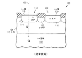
図1は、本発明の説明を補助するための、従来技術で公知のCMOSイメージセンサの部分を示す側面の概略的な断面図である。CMOSイメージセンサは、参照番号100により指示され、概して、基板102、基板102上のエピタキシャル(エピ)層104、アレイに配列されてエピ層104内に拡がる複数のピクセル(ピクセル110及び112の2つのみを図1に図解する)を含む。基板102及びエピ層104はどちらも、シリコン半導体材料からなるが、しかしながら基板102はP+(高濃度ドープP型)半導体材料から製造され、エピ層104はP-(低濃度ドープP型)半導体材料から製造されている。
FIG. 1 is a schematic cross-sectional side view showing portions of a CMOS image sensor known in the prior art to assist in the description of the present invention. A CMOS image sensor is indicated by
ピクセル110及び112は、ホトダイオードn-井戸114及び116をそれぞれ含み、またホトダイオードn-井戸114及び116上に堆積され、ピクセルに対する接触を改善する表面埋め込み領域118及び120をそれぞれ含む。ホトダイオードn-井戸114及び116は、N-(低濃度ドープN型)半導体材料から製造され、表面埋め込み領域118及び120は、N+(高濃度ドープN型)半導体材料から製造されている。P型半導体材料(図1に示すP-井戸122として指示する)は、ピクセル110及び112の間に設けられ、ピクセル間を絶縁する。
図1に概略的に図解するように、赤外線波長に対する遠赤外線(以降、概して赤外線波長と称する)の光130がピクセル素子110に衝突すると、光はイメージセンサ100のシリコンの表面より遙か下まで貫通し、電子-正孔対が基板102の深部で発生する。これらの深さは、ピクセルの収集領域の遙か下であり、したがって光生成キャリアが全ての方向に自由に拡散する。高濃度ドープシリコン基板102のような一般的な基板に対する電子の拡散距離は約5μmであり、ピクセル112のような隣接するピクセルに多くの電子が比較的容易に拡散し、クロストークを生じる。さらに、CMOSイメージセンサ100内では、図1に概略的に図解するようにそのピクセル自体に進むエピ層内で発生したキャリアとは区別されるように、深部で発生したキャリアの多くが基板内で再結合し、消失するので感度が低下する。
As illustrated schematically in FIG. 1, when far-infrared (hereinafter generally referred to as infrared wavelength)
図2Aは、本発明の例示的な実施態様によるCMOSイメージセンサの部分を示す側面の概略的な断面図である。イメージセンサは、概して参照番号200により指示され、図1のCMOSイメージセンサと同様に、基板202と、エピ層204と、ホトダイオードn-井戸214及び216並びに表面埋め込み領域218及び220をそれぞれ含むとともにエピ層204内に拡がるピクセル210及び212とを含む。また図1のCMOSイメージセンサと同様に、基板202はP+シリコン半導体材料を含み、エピ層204はP-シリコン半導体材料を含み、ホトダイオードn-井戸214及び216はN-半導体材料から形成され、表面埋め込み領域218及び220はN+半導体材料から形成されている。P型半導体材料(P-井戸222として指示する)は、ピクセル210と212の間に設けられ、ピクセル間を絶縁する。
FIG. 2A is a schematic cross-sectional side view showing portions of a CMOS image sensor according to an exemplary embodiment of the present invention. The image sensor is generally designated by the
図2AのCMOSイメージセンサ200は、図1のCMOSイメージセンサ100と異なり、エピ層204はエピ層104よりも厚く(例えば、図1のイメージセンサのような典型的なCMOSイメージセンサにおいては厚みが約2μm-6μmであるのに対して、約4μmから約20μmの厚みである)、より深いホトダイオードn-井戸214及び216を含む(図1のイメージセンサのような典型的なCMOSイメージセンサでは、約1μm-2μmの深さであるのに対して、例えば、エピ層204内に約2μmから約10μmの深さまで拡がる)。より厚いエピ層及びより深いホトダイオードn-井戸により、空乏層の深さはピクセルの表面の遙か下まで貫通する。
The
エピ層204は、低濃度ドープP型材料であり、空乏層の深さより下にあり、キャリアに導かれる電界をもたらすように段階的にドープされている。加えて、水平方向の障壁層224が、エピ層の傾斜部分の下、基板202とエピ層204の間に設けられている。水平方向の障壁層224は、水平方向の障壁層の下方の基板202内で発生したキャリアが隣接するピクセルに及び隣接するピクセル内に拡散してクロストークが生じることを防ぐように機能する。
Epi
CMOSイメージセンサ200内のホトダイオードn-井戸214及び216の深さが増大するので、多くのキャリアの収集が可能となり、したがってイメージセンサの感度が増大する。同時に、水平方向の障壁層224の下の基板202内で発生する電子は、基板内にとどまり再結合する。したがって、CMOSイメージセンサ200は、図1のイメージセンサと比較して、赤外線波長におけるクロストークを低減し、またより高い感度を有する。
As the depth of the photodiode n-
図2Bは、本発明の説明を補助するための、p型半導体における不純物添加障壁の機能を概略的に示す図である。示すように、半導体は、概して参照番号250により指示され、障壁254を形成し、電子256のような電子の移動を実質的に制御する高濃度ドープ領域252を含む。特に、矢印258により図解するように、電子256は障壁254を横切らない。このようにして、254のような障壁は、隣接するピクセル内に電子が拡散することを防ぎ、クロストークが生じることを防ぐのに利用される。
FIG. 2B is a diagram schematically showing the function of the impurity addition barrier in the p-type semiconductor to assist the explanation of the present invention. As shown, the semiconductor is generally indicated by
本発明の例示的な実施形態によれば、水平方向の障壁層224は、選択的な水平方向のドープによりもたらされる。高効率の障壁をもたらすために、厚みが約10 nm(100オングストローム)から約1μmであり、約1019/cm3から1020/cm3の範囲でドープされた非常に高濃度にホウ素をドープした層が利用される。また、障壁層224は、通常のCMOS製造プロセスの熱量に耐えることが可能でなければならないが、これは、通常の熱量は相当のホウ素の拡散を生じさせ、それによってホウ素は広がり、イメージセンサのホトダイオード領域内に拡散し、感度を低下させるので、適合させることは困難である。また、この外方への拡散は、障壁層内のホウ素の量を低減させ、その効果を低下させる。本発明の例示的な実施形態によれば、約3パーセント未満の濃度の炭素とともに障壁層を合金化することによって、ホウ素の拡散を低減させる。
According to an exemplary embodiment of the invention, the
水平方向の障壁層224を設けることに関連して生じる他の問題は、ホウ素と炭素の双方を付加することが障壁層の厚みを制限するシリコンの格子定数を低下させることである。本発明の例示的な実施形態によれば、ホウ素の外方への拡散を制限する一方で、格子応力を低減させるために、より厚い障壁層を、Geの付加による歪み補正により成長させることができる。一般に、拡散を制限し、格子歪みを緩和するために、水平方向の障壁層224は、本発明の例示的な実施形態によれば、ホウ素、アルミニウム、インジウム、燐、砒素、アンチモン、ゲルマニウム、炭素の1つ又はそれ以上を含む。
Another problem that arises in connection with providing the
本発明の例示的な実施形態によれば、また、水平方向の障壁層をもたらす高濃度にホウ素をドープされたSi層を、炭素を含む薄い層によって一方又は両方の側部をキャッピングすること又は封入することの何れかによりホウ素の外方への拡散を制限する一方で、格子歪みを低減することができる。さらに、Cドープ(炭素をドープされた)Si層でキャッピングすることにより、続く固体ソース拡散を実施することができる。 According to an exemplary embodiment of the invention, a heavily boron-doped Si layer that also provides a horizontal barrier layer may be capped on one or both sides with a thin layer comprising carbon, or Lattice distortion can be reduced while limiting the outward diffusion of boron by either encapsulation. In addition, subsequent solid source diffusion can be performed by capping with a C-doped (carbon doped) Si layer.
図3は、本発明のさらなる実施形態によるCMOSイメージセンサの部分を示す側面の概略的な断面図である。イメージセンサは、概して参照番号300により指示され、図2AのCMOSイメージセンサ200と同様であり、基板302、エピタキシャル層304、基板とエピタキシャル層の間の水平方向の障壁層324、ホトダイオードn-井戸314と316及び表面埋め込み領域318と320をそれぞれ含むピクセル310と312を含む。また、図2AのCMOSイメージセンサ200と同様に、基板302は、P+シリコン半導体材料を含み、エピ層304はP-シリコン半導体材料を含み、水平方向の障壁層324は非常に高濃度にホウ素をドープされた層を含み、ホトダイオードn-井戸314及び316はN-半導体材料から形成され、表面埋め込み領域318及び320はN+半導体材料から形成されている。P型半導体材料(P-井戸322として指示する)は、ピクセル310と312の間に設けられている。
FIG. 3 is a schematic cross-sectional side view showing portions of a CMOS image sensor according to a further embodiment of the present invention. The image sensor is generally indicated by
CMOSイメージセンサ300は、CMOSイメージセンサ200と異なり、隣接するピクセル310と312の間のP-井戸が図2AのP-井戸222よりも大幅に深く延伸し(図1のイメージセンサ100のような典型的なイメージセンサでは約1μm-2μmの深さであるのに対して、例えば、表面の下方約2μmから約20 μmの深さまで)、加えて各P-井戸322内に深いトレンチ326を含む。
特に、CMOSイメージセンサ200に設けられているようなより深いホトダイオード収集層に対して、エピ層内の横方向の拡散がクロストークを増大させる作用を有する。しかしながら、イメージセンサ300では、トレンチ326とともに深いP-井戸322が、隣接するピクセル間の横方向の障壁層として機能し、ピクセル間の横方向の拡散を防ぐ。トレンチは約0.5μmから約5μmの厚みを有し、P-井戸及びトレンチを含む横方向の障壁は、約1μmから約10 μmの厚みを有する。
In particular, for deeper photodiode collection layers such as those provided in
本発明の例示的な実施形態によれば、深いトレンチ326は、P-井戸分離体322が設けられる前に、形成されることが好ましい。これにより、ホウ素を素子内の深部に入れることができる。代替的に、トレンチ充填物としてP型ポリシリコンを堆積させ、さらにポリシリコン内でP型ドーパントを形成して拡散させることができる。窒化シリコン及び酸化シリコンを含む他のトレンチ充填物を利用することもできる。また、ドープされたSiO2(ホウケイ酸ガラス)を利用してホウ素をもたらすこともできる。
According to an exemplary embodiment of the present invention, the
イメージセンサ300では、n-井戸からの空乏領域又はp-n接合はトレンチに達してはならない。これは、トレンチの表面が表面エネルギー準位を含み、空乏領域がトレンチに達するならば、漏れ電流が生じ流れるためである。実際に、これはホウ素を拡散させるための主たる理由である。ホウ素は、N-井戸からの空乏領域がトレンチに達するのを防ぐ。また、トレンチの存在しない実施形態では同時に、ホウ素はピクセルの絶縁に役立つ。
In the
図4は、図3に図解するCMOSイメージセンサの部分を示す概略的な平面図である。特に、図4は、CMOSイメージセンサ300内の複数のピクセル402のそれぞれの間に設けられ、隣接するピクセル間で横方向の拡散を防ぐ横方向の障壁層を形成する図3のトレンチ326を画定するマスク404を図解する。
4 is a schematic plan view showing a portion of the CMOS image sensor illustrated in FIG. In particular, FIG. 4 defines the
したがって、CMOSイメージセンサ300は、より厚いエピ層及びより深いホトダイオード接合と関連して、赤外線波長における少ないクロストーク及び高い感度の双方をもたらす水平方向の障壁層324と、隣接するピクセル間の深いP-井戸324及びトレンチ326によって画定され、より深いホトダイオードの間の横方向の拡散を低減する横方向の障壁層を備えている。
Thus, the
したがって、本発明の例示的な実施形態によれば、より厚いエピ層及びより深いホトダイオード接合とともに、イメージセンサのエピ層と基板の間の1つ又はそれ以上の水平方向の障壁層と、隣接するピクセル間の横方向の障壁層とを有するCMOSイメージセンサは、特に赤外線波長に対する遠赤外線の光に対して高い感度と少ないクロストークとを備えたイメージセンサをもたらす。本発明は、780 nm又は840 nm用のAlGaAs/GaAsのような低価格の赤外線光源と関連してCMOSイメージセンサを使用する、コンピュータの光学式マウスのような動きを検出する用途及び、目の検出装置のような赤外線イメージング用途に対して特に適するが、本発明が、光の何らかの特定の波長、又は何らかの特定の用途で使用されることに限定されないことを理解されたい。赤外線光源は、網膜によるより高い反射率のため、及び被写体の注意をそらせることなく目の測定を行うことができるため、いずれにしても目の検出用途に対して特に望ましい。 Thus, according to an exemplary embodiment of the present invention, adjacent to one or more horizontal barrier layers between the epilayer of the image sensor and the substrate, along with a thicker epilayer and deeper photodiode junction. A CMOS image sensor with a lateral barrier layer between pixels results in an image sensor with high sensitivity and low crosstalk, especially for far-infrared light for infrared wavelengths. The present invention is intended for use in detecting motion such as an optical mouse in a computer using a CMOS image sensor in conjunction with a low-cost infrared light source such as AlGaAs / GaAs for 780 nm or 840 nm, and the eye. While particularly suitable for infrared imaging applications such as detection devices, it should be understood that the invention is not limited to being used in any particular wavelength of light, or in any particular application. Infrared light sources are particularly desirable for eye detection applications in any case because of the higher reflectivity of the retina and the ability to perform eye measurements without diverting the subject's attention.
図5-12は、本発明の例示的な実施形態によるCMOSイメージセンサを製造する方法の工程を概略的に図解する。特に、図5-12は、図3に図解するイメージセンサに設けられるようなトレンチを含まない、ピクセル間の横方向の障壁層を有するCMOSイメージセンサを製造する方法の工程を図解する。 5-12 schematically illustrate the steps of a method of manufacturing a CMOS image sensor according to an exemplary embodiment of the present invention. In particular, FIGS. 5-12 illustrate the steps of a method for manufacturing a CMOS image sensor having a lateral barrier layer between pixels that does not include a trench as provided in the image sensor illustrated in FIG.
先ず図5を参照すると、約5×10¹⁸にまで高濃度にホウ素をドープしたシリコンの開始ブロックが、502で示すように、最初に設けられる。本発明がP型ドーパントとしてホウ素に制限されないことを理解されたい。アルミニウム、ガリウム、インジウムを含む他のP型ドーパントを使用することができる。同様に、燐、砒素、アンチモンを含む他のN型ドーパントを使用することができる。さらに、シリコン上にLTO(低温熱酸化)の1000 nm(10000オングストローム)及び500 nm(5000オングストローム)厚の熱酸化層504が成長され、ホトレジスト層506がさらに酸化層上に適用される。
Referring first to FIG. 5, a starting block of silicon doped with boron up to about 5 × 10 18 is first provided, as indicated at 502. It should be understood that the present invention is not limited to boron as a P-type dopant. Other P-type dopants including aluminum, gallium, and indium can be used. Similarly, other N-type dopants including phosphorus, arsenic, and antimony can be used. Furthermore, a 1000 nm (10000 angstrom) and 500 nm (5000 angstrom) thick
図6を参照すると、さらに、508で示すようにホトレジスト層506内にパターンが現像される。図7に示すように、さらに、510で示すように、酸化層がエッチングされ、さらにホトレジスト層が、図7に示すように、取り除かれる。
Referring to FIG. 6, a pattern is further developed in the
さらに、図8の512で概略的に示すように、埋め込み酸化物が成長される。これは、シリコン内の工程で生じ、エピ層が適用された後、位置合わせされる。さらに高線量のホウ素が、複数のエネルギーにおいて注入される。514で概略的に示すように、これによりホウ素は異なる深さまで貫通し、したがって横方向の拡散障壁が形成される。本発明の例示的な実施形態による注入線量及びエネルギーは以下の通りである。
1. エネルギー30keV 線量2.9×10¹⁴
2. エネルギー60keV 線量5.8×10¹⁴
3. エネルギー90keV 線量6.4×10¹⁴
4. エネルギー120keV 線量7.7×10¹⁴
5. エネルギー180keV 線量1.15×10¹⁵
6. エネルギー240keV 線量1.34×10¹⁵
より高いエネルギーの注入は、エネルギー準位の半分で、二重イオン化ホウ素を注入することにより実施され得ることが認識されなければならない。
In addition, a buried oxide is grown as shown schematically at 512 in FIG. This occurs in a process in silicon and is aligned after the epi layer is applied. Higher doses of boron are implanted at multiple energies. As shown schematically at 514, this penetrates the boron to different depths, thus forming a lateral diffusion barrier. The implantation dose and energy according to an exemplary embodiment of the present invention is as follows.
1. Energy 30keV Dose 2.9 × 10 14
2. Energy 60keV Dose 5.8 × 10 14
3. Energy 90keV Dose 6.4 × 10 14
4. Energy 120keV Dose 7.7 × 10 14
5. Energy 180keV Dose 1.15 × 10 15
6. Energy 240keV Dose 1.34 × 10 15
It should be appreciated that higher energy implantation can be performed by implanting double ionized boron at half the energy level.
さらに、高温での焼鈍及び注入物の拡散が、図9の516で概略的に図解するように実施される。本発明の例示的な実施形態による障壁層の駆動手法は以下の通りである。
1. 850℃でN2を供給する
2. N2内で1000℃まで毎分5℃の割合で昇温する
3. N2内において1000℃、90分間焼鈍する
4. N2内で1125℃まで毎分3℃の割合で昇温する
5. 2.5%の酸素を含むN2内で、1125℃、220分間保持する
6. N2内で1000℃まで毎分3℃の割合で降温する
7. N2内において1000℃、240分間焼鈍する
8. N2内で850℃まで毎分3℃の割合で降温する
9. N2内にウエハを引き出す。
Further, high temperature annealing and implant diffusion are performed as schematically illustrated at 516 in FIG. The driving method of the barrier layer according to the exemplary embodiment of the present invention is as follows.
1. Supply N 2 at 850 ℃
2. Heat up to 1000 ° C at a rate of 5 ° C per minute in N 2
3. Annealing in N 2 at 1000 ° C for 90 minutes
4. Heat up to 1125 ° C at a rate of 3 ° C per minute in N 2
5. Hold at 1125 ° C for 220 minutes in N 2 containing 2.5% oxygen
6. Decrease the temperature at a rate of 3 ° C per minute up to 1000 ° C in N 2
7. Annealing in N 2 at 1000 ° C for 240 minutes
8. Lower the temperature to 850 ° C at a rate of 3 ° C per minute in N 2
9. pull out the wafer in N 2.
さらに、図10に示すように、酸化物が取り除かれ、p型エピ層518が、図11に示すように成長される。工程の後、横方向の障壁層(横方向のドープ障壁)520は、図12に示すように拡散される。上方に伸びる拡がり522は電子のより良好な閉じ込めを助ける。
Further, as shown in FIG. 10, the oxide is removed and a p-
図13-15は、本発明のさらなる例示的な実施形態によるCMOSイメージセンサを製造する方法の工程を概略的に図解する。特に、図13-15は、本発明の例示的な実施形態によるイメージセンサにおいて、イメージセンサのエピ層と基板の間の水平方向の障壁と、隣接するピクセル間の横方向の障壁層のどちらも有するCMOSイメージセンサを製造する方法の工程を概略的に図解する。 13-15 schematically illustrate the steps of a method of manufacturing a CMOS image sensor according to a further exemplary embodiment of the present invention. In particular, FIGS. 13-15 illustrate that in an image sensor according to an exemplary embodiment of the present invention, both the horizontal barrier between the epi layer of the image sensor and the substrate and the lateral barrier layer between adjacent pixels. 1 schematically illustrates the steps of a method for manufacturing a CMOS image sensor having the same.
最初に、図13に示すように、非常に高濃度にドープされた水平方向の障壁層(>1×10¹⁹のホウ素)614が、高濃度にドープされたシリコン基板(≒5×10¹⁸のホウ素)602の上部に形成される。さらに、固定された中程度の量ドープされた又は段階的にドープされたエピ層606が、水平方向の障壁層604の上に設けられる。段階的なドーピングプロファイルは、キャリアを上方に方向付け、収集効率を改善する電界をもたらす。
First, as shown in FIG. 13, a very highly doped horizontal barrier layer (> 1 × 10 19 boron) 614 is applied to a heavily doped silicon substrate (≈5 × 10 18 Boron) 602 is formed on top. In addition, a fixed medium quantity doped or step-doped
さらに、図5-12を参照して上述した横方向の障壁層とともにCMOSイメージセンサを製造する工程が実施され、図14に示すように、エピ層606内に横方向の障壁層610がもたらされる。最後に、さらに、低濃度にドープされたホトダイオードエピが、図15の612で示すように成長され、イメージセンサが完成する。
Further, a process of fabricating a CMOS image sensor with the lateral barrier layer described above with reference to FIGS. 5-12 is performed, resulting in a
本発明の例示的な実施形態を開示してきたが、本発明の範囲から逸脱することなく、本発明を種々の仕方で改変できることが認識されなければならない。例えば、本発明の例示的な実施形態は、CMOSイメージセンサを製造する方法を開示するが、本発明のイメージセンサは、本発明の範囲から逸脱することなく、多くの異なる方法で製造することができる。加えて、本明細書で開示するCMOSイメージセンサの特定の特性は、本発明の範囲から逸脱することなく、様々に変化させることができる。例えば、本明細書で開示するイメージセンサは、反対のドープ型、すなわちn+基板、n-エピ、n-井戸分離体、p-井戸ピクセル、p+接触を利用して製造することもできる。そのようなイメージセンサでは、障壁層はn+となる。概して、本明細書で使用する「CMOSイメージセンサ」は、CMOS工程で製造し、CMOS電子技術と互換性があり、一体化することができる任意のイメージセンサを含むことを意図している。 While exemplary embodiments of the invention have been disclosed, it should be appreciated that the invention can be modified in various ways without departing from the scope of the invention. For example, while the exemplary embodiments of the present invention disclose a method of manufacturing a CMOS image sensor, the image sensor of the present invention can be manufactured in many different ways without departing from the scope of the present invention. it can. In addition, the particular characteristics of the CMOS image sensor disclosed herein can be varied in various ways without departing from the scope of the present invention. For example, the image sensor disclosed herein can be fabricated using the opposite doped type, i.e. n + substrate, n-epi, n-well separator, p-well pixel, p + contact. In such an image sensor, the barrier layer is n +. In general, as used herein, a “CMOS image sensor” is intended to include any image sensor that is manufactured in a CMOS process, is compatible with CMOS electronics, and can be integrated.
本発明の例示的な実施形態が多くの仕方で変更可能であるので、本発明は、添付の特許請求の範囲の記載によって要求される範囲でのみ制限されることに理解されたい。 Since the exemplary embodiments of the invention can be varied in many ways, it should be understood that the invention is limited only to the extent required by the appended claims.
Claims (22)
前記基板上のエピタキシャル層と、
光を受容するための、前記エピタキシャル層内に拡がる複数のピクセルと、
前記基板内に発生したキャリアが前記エピタキシャル層に移動するのを防ぐための、前記基板と前記エピタキシャル層の間の水平方向の障壁層と、前記エピタキシャル層内の電子の横方向への拡散を防ぐための、前記複数のピクセルの隣接するもの同士の間の複数の横方向の障壁層との少なくとも1つとを含むCMOSイメージセンサ。 A substrate,
An epitaxial layer on the substrate;
A plurality of pixels extending in the epitaxial layer for receiving light;
A horizontal barrier layer between the substrate and the epitaxial layer for preventing carriers generated in the substrate from moving to the epitaxial layer, and preventing lateral diffusion of electrons in the epitaxial layer. And at least one of a plurality of lateral barrier layers between adjacent ones of the plurality of pixels.
前記基板上のエピタキシャル層と、
それぞれが前記エピタキシャル層内に拡がる光を受容するための複数のピクセルと、
前記基板内に発生したキャリアが前記エピタキシャル層に移動するのを防ぐための、前記基板と前記エピタキシャル層の間の水平方向の障壁層と、
前記エピタキシャル層内の電子の横方向への拡散を防ぐための、前記複数のピクセルの隣接するもの同士の間の複数の横方向の障壁層を含むCMOSイメージセンサ。 A substrate,
An epitaxial layer on the substrate;
A plurality of pixels each for receiving light extending into the epitaxial layer;
A horizontal barrier layer between the substrate and the epitaxial layer to prevent carriers generated in the substrate from moving to the epitaxial layer;
A CMOS image sensor comprising a plurality of lateral barrier layers between adjacent ones of the plurality of pixels to prevent lateral diffusion of electrons in the epitaxial layer.
前記基板内に発生したキャリアが前記エピタキシャル層に移動するのを防ぐための、前記基板と前記エピタキシャル層の間の水平方向の障壁層と、前記エピタキシャル層内の電子の横方向への拡散を防ぐための、前記複数のピクセルの隣接するもの同士の間の複数の横方向の障壁層との少なくとも1つを形成することを含む方法。 A method of manufacturing a CMOS image sensor comprising a substrate, an epitaxial layer on the substrate, and a plurality of pixels extending in the epitaxial layer,
A horizontal barrier layer between the substrate and the epitaxial layer for preventing carriers generated in the substrate from moving to the epitaxial layer, and preventing lateral diffusion of electrons in the epitaxial layer. Forming at least one of a plurality of lateral barrier layers between adjacent ones of the plurality of pixels.
Applications Claiming Priority (1)
| Application Number | Priority Date | Filing Date | Title |
|---|---|---|---|
| US11/197,004 US7307327B2 (en) | 2005-08-04 | 2005-08-04 | Reduced crosstalk CMOS image sensors |
Publications (2)
| Publication Number | Publication Date |
|---|---|
| JP2007067393A true JP2007067393A (en) | 2007-03-15 |
| JP2007067393A5 JP2007067393A5 (en) | 2009-09-17 |
Family
ID=36950808
Family Applications (1)
| Application Number | Title | Priority Date | Filing Date |
|---|---|---|---|
| JP2006212759A Withdrawn JP2007067393A (en) | 2005-08-04 | 2006-08-04 | Reduced crosstalk cmos image sensor |
Country Status (5)
| Country | Link |
|---|---|
| US (2) | US7307327B2 (en) |
| EP (1) | EP1750308B1 (en) |
| JP (1) | JP2007067393A (en) |
| CN (1) | CN1933169A (en) |
| TW (1) | TW200721468A (en) |
Cited By (8)
| Publication number | Priority date | Publication date | Assignee | Title |
|---|---|---|---|---|
| JP2008218968A (en) * | 2007-03-06 | 2008-09-18 | Taiwan Semiconductor Manufacturing Co Ltd | Method for manufacturing semiconductor device, and image sensor device |
| JP2010541294A (en) * | 2007-10-08 | 2010-12-24 | インシアヴァ (ピーテーワイ) リミテッド | Silicon light emitting device using carrier injection |
| JP2011077498A (en) * | 2009-09-02 | 2011-04-14 | Sony Corp | Solid-state imaging apparatus and method for manufacturing the same |
| JP2011222900A (en) * | 2010-04-14 | 2011-11-04 | Hamamatsu Photonics Kk | Solid-state imaging apparatus |
| JP2015056622A (en) * | 2013-09-13 | 2015-03-23 | 株式会社リコー | Semiconductor device |
| JP2015095484A (en) * | 2013-11-08 | 2015-05-18 | ルネサスエレクトロニクス株式会社 | Semiconductor device and method for manufacturing the same |
| JP2021034423A (en) * | 2019-08-19 | 2021-03-01 | コーデンシ株式会社 | Segmented photodiode and method for manufacturing segmented photodiode |
| US11346953B2 (en) | 2018-07-20 | 2022-05-31 | Kabushiki Kaisha Toshiba | Photo detector, photo detection system, lidar device and vehicle |
Families Citing this family (62)
| Publication number | Priority date | Publication date | Assignee | Title |
|---|---|---|---|---|
| US20060049464A1 (en) | 2004-09-03 | 2006-03-09 | Rao G R Mohan | Semiconductor devices with graded dopant regions |
| US7307327B2 (en) | 2005-08-04 | 2007-12-11 | Micron Technology, Inc. | Reduced crosstalk CMOS image sensors |
| US7728277B2 (en) * | 2005-11-16 | 2010-06-01 | Eastman Kodak Company | PMOS pixel structure with low cross talk for active pixel image sensors |
| KR100719361B1 (en) * | 2005-11-22 | 2007-05-17 | 삼성전자주식회사 | Cmos image sensor and method of forming the same |
| KR100809323B1 (en) * | 2006-01-31 | 2008-03-05 | 삼성전자주식회사 | Image sensor with improved sensitivity and decreased crosstalk and fabrication method thereof |
| KR100703987B1 (en) * | 2006-05-17 | 2007-04-09 | 삼성전자주식회사 | Fabricating method of image sensor and image sensor fabricated thereby |
| KR100853788B1 (en) * | 2006-11-27 | 2008-08-25 | 동부일렉트로닉스 주식회사 | Method for Measuring Thickness of Layer in Image Sensor and Pattern Therefor |
| CN101304035B (en) * | 2007-05-08 | 2010-06-09 | 中芯国际集成电路制造(上海)有限公司 | Image sensor and method for forming the same |
| US8237832B2 (en) | 2008-05-30 | 2012-08-07 | Omnivision Technologies, Inc. | Image sensor with focusing interconnections |
| WO2010009462A2 (en) * | 2008-07-18 | 2010-01-21 | Massachusetts Institute Of Technology | Dark current reduction for large area photodiodes |
| US8237206B2 (en) * | 2008-08-12 | 2012-08-07 | United Microelectronics Corp. | CMOS image sensor, method of making the same, and method of suppressing dark leakage and crosstalk for CMOS image sensor |
| US8269985B2 (en) | 2009-05-26 | 2012-09-18 | Zena Technologies, Inc. | Determination of optimal diameters for nanowires |
| US9299866B2 (en) | 2010-12-30 | 2016-03-29 | Zena Technologies, Inc. | Nanowire array based solar energy harvesting device |
| US8889455B2 (en) | 2009-12-08 | 2014-11-18 | Zena Technologies, Inc. | Manufacturing nanowire photo-detector grown on a back-side illuminated image sensor |
| US8748799B2 (en) | 2010-12-14 | 2014-06-10 | Zena Technologies, Inc. | Full color single pixel including doublet or quadruplet si nanowires for image sensors |
| US8299472B2 (en) | 2009-12-08 | 2012-10-30 | Young-June Yu | Active pixel sensor with nanowire structured photodetectors |
| US8791470B2 (en) | 2009-10-05 | 2014-07-29 | Zena Technologies, Inc. | Nano structured LEDs |
| US8546742B2 (en) | 2009-06-04 | 2013-10-01 | Zena Technologies, Inc. | Array of nanowires in a single cavity with anti-reflective coating on substrate |
| US8274039B2 (en) | 2008-11-13 | 2012-09-25 | Zena Technologies, Inc. | Vertical waveguides with various functionality on integrated circuits |
| US8519379B2 (en) | 2009-12-08 | 2013-08-27 | Zena Technologies, Inc. | Nanowire structured photodiode with a surrounding epitaxially grown P or N layer |
| US9082673B2 (en) | 2009-10-05 | 2015-07-14 | Zena Technologies, Inc. | Passivated upstanding nanostructures and methods of making the same |
| US8507840B2 (en) | 2010-12-21 | 2013-08-13 | Zena Technologies, Inc. | Vertically structured passive pixel arrays and methods for fabricating the same |
| US9478685B2 (en) | 2014-06-23 | 2016-10-25 | Zena Technologies, Inc. | Vertical pillar structured infrared detector and fabrication method for the same |
| US8835831B2 (en) | 2010-06-22 | 2014-09-16 | Zena Technologies, Inc. | Polarized light detecting device and fabrication methods of the same |
| US9515218B2 (en) | 2008-09-04 | 2016-12-06 | Zena Technologies, Inc. | Vertical pillar structured photovoltaic devices with mirrors and optical claddings |
| US8890271B2 (en) | 2010-06-30 | 2014-11-18 | Zena Technologies, Inc. | Silicon nitride light pipes for image sensors |
| US8866065B2 (en) | 2010-12-13 | 2014-10-21 | Zena Technologies, Inc. | Nanowire arrays comprising fluorescent nanowires |
| US8735797B2 (en) | 2009-12-08 | 2014-05-27 | Zena Technologies, Inc. | Nanowire photo-detector grown on a back-side illuminated image sensor |
| US9000353B2 (en) | 2010-06-22 | 2015-04-07 | President And Fellows Of Harvard College | Light absorption and filtering properties of vertically oriented semiconductor nano wires |
| US8384007B2 (en) | 2009-10-07 | 2013-02-26 | Zena Technologies, Inc. | Nano wire based passive pixel image sensor |
| US9406709B2 (en) | 2010-06-22 | 2016-08-02 | President And Fellows Of Harvard College | Methods for fabricating and using nanowires |
| US9343490B2 (en) | 2013-08-09 | 2016-05-17 | Zena Technologies, Inc. | Nanowire structured color filter arrays and fabrication method of the same |
| US8229255B2 (en) | 2008-09-04 | 2012-07-24 | Zena Technologies, Inc. | Optical waveguides in image sensors |
| US20100148230A1 (en) * | 2008-12-11 | 2010-06-17 | Stevens Eric G | Trench isolation regions in image sensors |
| EP2202795A1 (en) | 2008-12-24 | 2010-06-30 | S.O.I. TEC Silicon | Method for fabricating a semiconductor substrate and semiconductor substrate |
| JP5564874B2 (en) * | 2009-09-25 | 2014-08-06 | ソニー株式会社 | Solid-state imaging device and electronic apparatus |
| US8502271B2 (en) * | 2009-10-23 | 2013-08-06 | Lockheed Martin Corporation | Barrier photodetector with planar top layer |
| KR101829480B1 (en) * | 2010-04-09 | 2018-02-14 | 씬트-엑스 에이비 | An x-ray sensor system and an x-ray imaging system |
| US8692198B2 (en) * | 2010-04-21 | 2014-04-08 | Sionyx, Inc. | Photosensitive imaging devices and associated methods |
| US8482090B2 (en) | 2010-07-15 | 2013-07-09 | Exelis, Inc. | Charged particle collector for a CMOS imager |
| JP5726005B2 (en) * | 2010-08-02 | 2015-05-27 | アイメックImec | Method for manufacturing CMOS imaging device array |
| US8507962B2 (en) | 2010-10-04 | 2013-08-13 | International Business Machines Corporation | Isolation structures for global shutter imager pixel, methods of manufacture and design structures |
| TWI459547B (en) | 2010-11-04 | 2014-11-01 | Novatek Microelectronics Corp | Image sensor |
| CN102222678A (en) * | 2011-06-22 | 2011-10-19 | 格科微电子(上海)有限公司 | CMOS (Complementary Metal Oxide Semiconductor) image sensor and forming method thereof |
| TWI455298B (en) * | 2011-10-25 | 2014-10-01 | Pixart Imaging Inc | Photosensor device and method for determining incident light |
| US8786023B2 (en) * | 2011-12-08 | 2014-07-22 | Contour Semiconductor, Inc. | Embedded non-volatile memory |
| US9093373B2 (en) * | 2013-08-13 | 2015-07-28 | Taiwan Semiconductor Manufacturing Co., Ltd. | Conductive diffusion barrier structure for ohmic contacts |
| US9331116B2 (en) * | 2014-01-15 | 2016-05-03 | Omnivision Technologies, Inc. | Back side illuminated single photon avalanche diode imaging sensor with high short wavelength detection efficiency |
| US9312408B2 (en) | 2014-06-12 | 2016-04-12 | Stmicroelectronics Sa | Imager having a reduced dark current through an increased bulk doping level |
| CN104065853B (en) * | 2014-06-16 | 2017-02-15 | 北京航空航天大学 | Infrared camera crosstalk eliminating method |
| KR102268712B1 (en) | 2014-06-23 | 2021-06-28 | 삼성전자주식회사 | Auto-focus image sensor and digital image processing device having the sensor |
| US9209320B1 (en) | 2014-08-07 | 2015-12-08 | Omnivision Technologies, Inc. | Method of fabricating a single photon avalanche diode imaging sensor |
| US20160219702A1 (en) | 2015-01-23 | 2016-07-28 | Gholamreza Chaji | Selective micro device transfer to receiver substrate |
| US10700120B2 (en) | 2015-01-23 | 2020-06-30 | Vuereal Inc. | Micro device integration into system substrate |
| US10134803B2 (en) | 2015-01-23 | 2018-11-20 | Vuereal Inc. | Micro device integration into system substrate |
| WO2017149521A1 (en) * | 2016-03-04 | 2017-09-08 | Vuereal Inc. | Micro device integration into system substrate |
| US10847571B2 (en) | 2015-01-23 | 2020-11-24 | Vuereal Inc. | Micro device integration into system substrate |
| RU2720538C2 (en) | 2016-01-28 | 2020-05-12 | Сэн-Гобэн Гласс Франс | Method of glass bending supported by excessive pressure and device suitable for this purpose |
| CN107293559A (en) * | 2016-04-05 | 2017-10-24 | 格科微电子(上海)有限公司 | RGBIR imaging sensors |
| US10672934B2 (en) * | 2017-10-31 | 2020-06-02 | Taiwan Semiconductor Manufacturing Company Ltd. | SPAD image sensor and associated fabricating method |
| US10418402B2 (en) * | 2017-11-30 | 2019-09-17 | Stmicroelectronics (Research & Development) Limited | Near ultraviolet photocell |
| US10892295B2 (en) * | 2018-01-10 | 2021-01-12 | Microsoft Technology Licensing, Llc | Germanium-modified, back-side illuminated optical sensor |
Family Cites Families (19)
| Publication number | Priority date | Publication date | Assignee | Title |
|---|---|---|---|---|
| US5859462A (en) * | 1997-04-11 | 1999-01-12 | Eastman Kodak Company | Photogenerated carrier collection of a solid state image sensor array |
| JP4131031B2 (en) * | 1998-03-17 | 2008-08-13 | ソニー株式会社 | Semiconductor device having light receiving element, optical pickup device, and method of manufacturing semiconductor device having light receiving element |
| JP3457551B2 (en) * | 1998-11-09 | 2003-10-20 | 株式会社東芝 | Solid-state imaging device |
| JP3370298B2 (en) * | 1999-07-27 | 2003-01-27 | シャープ株式会社 | Photodetector with built-in circuit |
| US6593607B1 (en) | 1999-09-30 | 2003-07-15 | Pictos Technologies, Inc. | Image sensor with enhanced blue response and signal cross-talk suppression |
| JP2002203954A (en) * | 2000-10-31 | 2002-07-19 | Sharp Corp | Light receiving element with built-in circuit |
| JP4270742B2 (en) | 2000-11-30 | 2009-06-03 | Necエレクトロニクス株式会社 | Solid-state imaging device |
| US20030082882A1 (en) * | 2001-10-31 | 2003-05-01 | Babcock Jeffrey A. | Control of dopant diffusion from buried layers in bipolar integrated circuits |
| JP2003224253A (en) * | 2002-01-31 | 2003-08-08 | Sanyo Electric Co Ltd | Optical semiconductor integrated circuit device and its manufacturing method |
| JP3754961B2 (en) * | 2002-02-22 | 2006-03-15 | キヤノン株式会社 | Solid-state imaging device and camera |
| JP4342142B2 (en) * | 2002-03-22 | 2009-10-14 | 富士通マイクロエレクトロニクス株式会社 | Semiconductor photo detector |
| US6740905B1 (en) * | 2002-11-12 | 2004-05-25 | Texas Instruments Incorporated | Apparatus for suppressing crosstalk in image sensors without degrading red light response |
| US7087944B2 (en) | 2003-01-16 | 2006-08-08 | Micron Technology, Inc. | Image sensor having a charge storage region provided within an implant region |
| JP3621400B2 (en) * | 2003-03-03 | 2005-02-16 | 松下電器産業株式会社 | Solid-state imaging device and manufacturing method thereof |
| JP4228887B2 (en) * | 2003-04-02 | 2009-02-25 | ソニー株式会社 | Solid-state imaging device and manufacturing method thereof |
| JP4841249B2 (en) * | 2003-06-30 | 2011-12-21 | ローム株式会社 | Image sensor and method for forming photodiode separation structure |
| KR100630679B1 (en) * | 2003-12-17 | 2006-10-02 | 삼성전자주식회사 | Photodiode and method for fabricating the same |
| US7342268B2 (en) * | 2004-12-23 | 2008-03-11 | International Business Machines Corporation | CMOS imager with Cu wiring and method of eliminating high reflectivity interfaces therefrom |
| US7307327B2 (en) | 2005-08-04 | 2007-12-11 | Micron Technology, Inc. | Reduced crosstalk CMOS image sensors |
-
2005
- 2005-08-04 US US11/197,004 patent/US7307327B2/en active Active
-
2006
- 2006-07-24 EP EP06015356A patent/EP1750308B1/en not_active Expired - Fee Related
- 2006-07-27 TW TW095127523A patent/TW200721468A/en unknown
- 2006-08-04 CN CNA2006101038463A patent/CN1933169A/en active Pending
- 2006-08-04 JP JP2006212759A patent/JP2007067393A/en not_active Withdrawn
-
2007
- 2007-11-15 US US11/940,569 patent/US7592654B2/en active Active
Cited By (9)
| Publication number | Priority date | Publication date | Assignee | Title |
|---|---|---|---|---|
| JP2008218968A (en) * | 2007-03-06 | 2008-09-18 | Taiwan Semiconductor Manufacturing Co Ltd | Method for manufacturing semiconductor device, and image sensor device |
| JP4718532B2 (en) * | 2007-03-06 | 2011-07-06 | 台湾積體電路製造股▲ふん▼有限公司 | Semiconductor device manufacturing method and image sensor device |
| JP2010541294A (en) * | 2007-10-08 | 2010-12-24 | インシアヴァ (ピーテーワイ) リミテッド | Silicon light emitting device using carrier injection |
| JP2011077498A (en) * | 2009-09-02 | 2011-04-14 | Sony Corp | Solid-state imaging apparatus and method for manufacturing the same |
| JP2011222900A (en) * | 2010-04-14 | 2011-11-04 | Hamamatsu Photonics Kk | Solid-state imaging apparatus |
| JP2015056622A (en) * | 2013-09-13 | 2015-03-23 | 株式会社リコー | Semiconductor device |
| JP2015095484A (en) * | 2013-11-08 | 2015-05-18 | ルネサスエレクトロニクス株式会社 | Semiconductor device and method for manufacturing the same |
| US11346953B2 (en) | 2018-07-20 | 2022-05-31 | Kabushiki Kaisha Toshiba | Photo detector, photo detection system, lidar device and vehicle |
| JP2021034423A (en) * | 2019-08-19 | 2021-03-01 | コーデンシ株式会社 | Segmented photodiode and method for manufacturing segmented photodiode |
Also Published As
| Publication number | Publication date |
|---|---|
| EP1750308A3 (en) | 2009-03-11 |
| TW200721468A (en) | 2007-06-01 |
| CN1933169A (en) | 2007-03-21 |
| US7307327B2 (en) | 2007-12-11 |
| EP1750308B1 (en) | 2011-02-23 |
| US20070029589A1 (en) | 2007-02-08 |
| US20080079045A1 (en) | 2008-04-03 |
| EP1750308A2 (en) | 2007-02-07 |
| US7592654B2 (en) | 2009-09-22 |
Similar Documents
| Publication | Publication Date | Title |
|---|---|---|
| JP2007067393A (en) | Reduced crosstalk cmos image sensor | |
| EP1681722B1 (en) | Multilayered semiconductor substrate and image sensor formed thereon for improved infrared response | |
| JP4020309B2 (en) | CMOS image sensor and manufacturing method thereof | |
| JP4718875B2 (en) | Solid-state image sensor | |
| US8035186B2 (en) | Low-noise semiconductor photodetectors | |
| JP5100988B2 (en) | Image sensor and manufacturing method thereof | |
| US7705380B2 (en) | Amplification-type solid-state image sensing device | |
| US20060186505A1 (en) | Image sensor cells | |
| US7749798B2 (en) | Optimized photodiode process for improved transfer gate leakage | |
| JP2008021875A (en) | Solid-state imaging apparatus | |
| JP6302216B2 (en) | Semiconductor device and manufacturing method thereof | |
| US10325955B2 (en) | CMOS image sensor with backside biased substrate | |
| TW200818476A (en) | Image sensor with improved color crosstalk | |
| WO2017094277A1 (en) | Avalanche photodiode | |
| JP2007027730A (en) | Image sensor and its manufacture | |
| US7642116B1 (en) | Method of forming a photodiode that reduces the effects of surface recombination sites | |
| US7199412B2 (en) | Image sensor with surface regions of different doping | |
| KR100595876B1 (en) | Method for fabricating photodiode of image sensor | |
| US6627475B1 (en) | Buried photodiode structure for CMOS image sensor | |
| JP2008300537A (en) | Solid-state imaging device | |
| KR20060108017A (en) | Cmos image sensor and method of fabricating the same | |
| US20100289107A1 (en) | Photodiode with interfacial charge control by implantation and associated process | |
| CN111446269B (en) | CMOS image sensor structure and manufacturing method | |
| KR20070017029A (en) | Reduced crosstalk cmos image sensors | |
| KR100622068B1 (en) | Cmos active pixel of image sensor for reducing dark current |
Legal Events
| Date | Code | Title | Description |
|---|---|---|---|
| A711 | Notification of change in applicant |
Free format text: JAPANESE INTERMEDIATE CODE: A711 Effective date: 20080222 |
|
| A521 | Request for written amendment filed |
Free format text: JAPANESE INTERMEDIATE CODE: A821 Effective date: 20080604 |
|
| RD02 | Notification of acceptance of power of attorney |
Free format text: JAPANESE INTERMEDIATE CODE: A7422 Effective date: 20080604 |
|
| A521 | Request for written amendment filed |
Free format text: JAPANESE INTERMEDIATE CODE: A523 Effective date: 20090727 Free format text: JAPANESE INTERMEDIATE CODE: A821 Effective date: 20090727 |
|
| A621 | Written request for application examination |
Free format text: JAPANESE INTERMEDIATE CODE: A621 Effective date: 20090727 |
|
| A521 | Request for written amendment filed |
Free format text: JAPANESE INTERMEDIATE CODE: A821 Effective date: 20090727 |
|
| A521 | Request for written amendment filed |
Free format text: JAPANESE INTERMEDIATE CODE: A821 Effective date: 20101004 |
|
| A761 | Written withdrawal of application |
Free format text: JAPANESE INTERMEDIATE CODE: A761 Effective date: 20101004 |