JP2007019488A - Semiconductor light emitting element - Google Patents
Semiconductor light emitting element Download PDFInfo
- Publication number
- JP2007019488A JP2007019488A JP2006159459A JP2006159459A JP2007019488A JP 2007019488 A JP2007019488 A JP 2007019488A JP 2006159459 A JP2006159459 A JP 2006159459A JP 2006159459 A JP2006159459 A JP 2006159459A JP 2007019488 A JP2007019488 A JP 2007019488A
- Authority
- JP
- Japan
- Prior art keywords
- layer
- light emitting
- type gan
- semiconductor light
- wavelength
- Prior art date
- Legal status (The legal status is an assumption and is not a legal conclusion. Google has not performed a legal analysis and makes no representation as to the accuracy of the status listed.)
- Pending
Links
Images


Abstract
Description
本発明は、半導体発光素子に関し、特にGaN系半導体発光素子に関する。 The present invention relates to a semiconductor light emitting device, and more particularly to a GaN-based semiconductor light emitting device.
近年、青色の半導体発光素子として、GaN系半導体を用いた半導体発光素子が知られている。青色の半導体発光素子と、黄色の発光体を組み合わせた白色LEDは携帯電話などのLCDバックライト用として需要が増大している。また、白色LEDは低消費電力、長寿命という特徴をもっていることから、次は蛍光灯、白熱灯などに変わる光源としての利用が期待されている。 In recent years, semiconductor light emitting devices using GaN-based semiconductors are known as blue semiconductor light emitting devices. White LEDs, which are a combination of a blue semiconductor light emitting element and a yellow light emitter, are increasing in demand for LCD backlights for mobile phones and the like. In addition, since white LEDs have the characteristics of low power consumption and long life, they are expected to be used as light sources that are replaced with fluorescent lamps, incandescent lamps, and the like.
従来のGaN系半導体発光素子では、サファイア基板上に、GaNバッファ層、n型GaN層、発光層、p型GaN層が順次結晶成長された構造となっている。しかしながら、従来のこのような構造では、p型GaN層の屈折率と、p型GaN層に接する空気や樹脂の屈折率との差が大きく、p型GaN層とp型GaN層に接する空気や樹脂との界面での全反射角が小さくなってしまうため、発光層で発生した光の多くがp型GaN層に接する空気や樹脂との界面で全反射し、光取り出し効率が低いという問題があった。 A conventional GaN-based semiconductor light-emitting device has a structure in which a GaN buffer layer, an n-type GaN layer, a light-emitting layer, and a p-type GaN layer are sequentially grown on a sapphire substrate. However, in such a conventional structure, the difference between the refractive index of the p-type GaN layer and the refractive index of air or resin in contact with the p-type GaN layer is large. Since the total reflection angle at the interface with the resin becomes small, most of the light generated in the light emitting layer is totally reflected at the interface with the air and the resin in contact with the p-type GaN layer, and the light extraction efficiency is low. there were.
たとえば、半導体発光素子が空気中で発光しているとすると、GaNの屈折率は光の波長が450nmのときに約2.5であるので、p型GaN層と空気との界面での全反射角は、約24°と小さい。発光層から放射され、この全反射角よりも大きな角度でp型GaN層と空気との界面に入射した光は、p型GaN層と空気との界面で全反射されるため半導体発光素子から取り出すことができない。 For example, assuming that the semiconductor light emitting device emits light in the air, the refractive index of GaN is about 2.5 when the wavelength of light is 450 nm, and thus total reflection at the interface between the p-type GaN layer and air. The angle is as small as about 24 °. Light emitted from the light emitting layer and incident on the interface between the p-type GaN layer and air at an angle larger than the total reflection angle is totally reflected at the interface between the p-type GaN layer and air, and thus is extracted from the semiconductor light emitting device. I can't.
この問題に対して、p型GaN層に発光波長程度の間隔で凹凸を周期的に形成する方法が提案されている(たとえば特許文献1)。この構造では、周期的に形成された凹凸による回折効果により発光層から放射される光の進行方向が変わり、全反射とならない角度に光が回折されるため、半導体発光素子の光取り出し効率が向上する。 To solve this problem, a method has been proposed in which irregularities are periodically formed in the p-type GaN layer at intervals of about the emission wavelength (for example, Patent Document 1). In this structure, the traveling direction of the light emitted from the light emitting layer is changed by the diffraction effect due to the irregularities formed periodically, and the light is diffracted at an angle that does not cause total reflection, thereby improving the light extraction efficiency of the semiconductor light emitting device. To do.
このような周期的に形成された凹凸をp型GaN層に形成する場合、まず結晶成長させたp型GaN層上にレジストを形成し、干渉露光法などによりレジストパターンを形成する。その後、RIE法などのドライエッチングによりレジストパターンに覆われていない部分を除去することによって、p型GaN層に凹凸が形成される。
しかしながら、p型GaN層をドライエッチングによってエッチングした場合、プラズマダメージにより、エッチングされたp型GaN層の表面に窒素空孔が生じる。この窒素空孔はドナーとして働くため、エッチングされたp型GaN層の表面にはn型化された部分が生じることになる。p型GaN層の表面の一部にn型化された部分が存在すると、その部分についてはn/p接合が存在するのにn側から+バイアスされるため、逆バイアス状態になり、結果として半導体発光素子の順方向電圧が上昇してしまう。また、n型化された部分は発光層に注入される電流が減少するうえ、p型GaN層の抵抗は高く、電流ひろがりがないため、結局半導体発光素子の有効な発光領域が減少してしまう。 However, when the p-type GaN layer is etched by dry etching, nitrogen vacancies are generated on the surface of the etched p-type GaN layer due to plasma damage. Since this nitrogen vacancy acts as a donor, an n-type portion is generated on the surface of the etched p-type GaN layer. If there is an n-type portion on a part of the surface of the p-type GaN layer, the n / p junction is present and the portion is + biased from the n side, resulting in a reverse bias state. The forward voltage of the semiconductor light emitting device is increased. In addition, since the current injected into the light emitting layer is reduced in the n-type portion, and the resistance of the p-type GaN layer is high and there is no current spread, the effective light emitting region of the semiconductor light emitting element eventually decreases. .
そのため、p型GaN層のn型化された部分は、ウェットエッチングなどの方法により除去する必要があるが、GaNのウェットエッチングは難しく、完全に除去することは困難であり、また製造工程が増えるため製造コストが増加する。 Therefore, it is necessary to remove the n-type portion of the p-type GaN layer by a method such as wet etching, but wet etching of GaN is difficult and difficult to remove completely, and the number of manufacturing processes increases. Therefore, the manufacturing cost increases.
本発明はこうした状況に鑑みなされたものであり、その目的は、光取り出し効率を向上した半導体発光素子の提供にある。 The present invention has been made in view of such a situation, and an object thereof is to provide a semiconductor light emitting device having improved light extraction efficiency.
上記課題を解決するために、本発明のある態様の半導体発光素子は、基板上に、n型GaN層と、発光層と、p型GaN層とが積層された半導体発光素子であって、p型GaN層上にMgxZn1−xO層(0≦x≦0.5)が設けられ、MgxZn1−xO層(0≦x≦0.5)の表面に、2次元の周期的な間隔で凹部または凸部が形成される。 In order to solve the above problems, a semiconductor light emitting device according to an aspect of the present invention is a semiconductor light emitting device in which an n-type GaN layer, a light emitting layer, and a p-type GaN layer are stacked on a substrate, A Mg x Zn 1-x O layer (0 ≦ x ≦ 0.5) is provided on the type GaN layer, and a two-dimensional surface is formed on the surface of the Mg x Zn 1-x O layer (0 ≦ x ≦ 0.5). Concave portions or convex portions are formed at periodic intervals.
この態様によると、MgxZn1−xO層(0≦x≦0.5)の表面に2次元の周期的な間隔で凹部または凸部が形成されているため、発光層からの光が回折される。回折光のうち、MgxZn1−xO層(0≦x≦0.5)とそれに接する媒体との界面での全反射角よりも小さい角度で界面に入射した回折光は、全反射されずに半導体発光素子の外部に取り出される。p型GaN層ではなく、MgxZn1−xO層(0≦x≦0.5)に凹部または凸部を形成しているため、ドライエッチングの際のプラズマはp型GaN層に直接さらされることがなく、ダメージによるp型GaN層表面のn型化は起こらないので、順方向電圧を上昇させることなく、光取り出し効率を向上させることができる。また、従来必要であったドライエッチング後のウェットエッチングの工程が不要となるので、製造コストを削減することができる。 According to this aspect, since the recesses or projections are formed on the surface of the Mg x Zn 1-x O layer (0 ≦ x ≦ 0.5) at two-dimensional periodic intervals, light from the light emitting layer is not emitted. Diffracted. Of the diffracted light, diffracted light incident on the interface at a smaller angle than the total reflection angle at the interface between the Mg x Zn 1-x O layer (0 ≦ x ≦ 0.5) and the medium in contact with the Mg x Zn 1-x O layer is totally reflected. Without being taken out of the semiconductor light emitting device. Since recesses or protrusions are formed in the Mg x Zn 1-x O layer (0 ≦ x ≦ 0.5), not the p-type GaN layer, the plasma during dry etching is directly exposed to the p-type GaN layer. Therefore, the p-type GaN layer surface does not become n-type due to damage, so that the light extraction efficiency can be improved without increasing the forward voltage. In addition, since the wet etching process after dry etching, which has been conventionally required, becomes unnecessary, the manufacturing cost can be reduced.
MgxZn1−xO層(0≦x≦0.5)に形成される凹部または凸部は、正方格子状または三角格子状に配置されてもよい。正方格子状に配置した場合、2次元の周期的な間隔で凹部または凸部を形成することができる。三角格子状に配置した場合は、2次元の周期的な間隔で形成する凹部または凸部の密度を高くすることができ、好適に光取り出し効率を向上させることができる。 The recesses or protrusions formed in the Mg x Zn 1-x O layer (0 ≦ x ≦ 0.5) may be arranged in a square lattice shape or a triangular lattice shape. When arranged in a square lattice shape, concave portions or convex portions can be formed at two-dimensional periodic intervals. When arranged in a triangular lattice shape, the density of the concave portions or convex portions formed at two-dimensional periodic intervals can be increased, and the light extraction efficiency can be preferably improved.
本発明の別の態様もまた、半導体発光素子である。この半導体発光素子は、p型GaN層と、発光層と、n型GaN層とが積層された半導体発光素子であって、n型GaN層の表面に、2次元の周期的な間隔で凹部または凸部が形成される。 Another embodiment of the present invention is also a semiconductor light emitting device. This semiconductor light-emitting device is a semiconductor light-emitting device in which a p-type GaN layer, a light-emitting layer, and an n-type GaN layer are stacked, and has recesses or recesses on the surface of the n-type GaN layer at two-dimensional periodic intervals. A convex part is formed.
この態様によると、n型GaN層の表面に2次元の周期的な間隔で凹部または凸部が形成されているため、発光層からの光が回折される。回折光のうち、n型GaN層とそれに接する媒体との界面での全反射角よりも小さい角度で界面に入射した回折光は、全反射されずに半導体発光素子の外部に取り出される。n型GaN層をドライエッチングすることによっても窒素空孔が発生し、n型GaN層16の表面がn型化するが、n型GaN層は元来n型であるから逆バイアスが印加される状態にはならず、順方向電圧が上昇することなく、光取り出し効率を向上させることができる。この場合も、従来必要であったドライエッチング後のウェットエッチングの工程が不要となるので、製造コストを削減することができる。
According to this aspect, since the concave portions or the convex portions are formed on the surface of the n-type GaN layer at two-dimensional periodic intervals, the light from the light emitting layer is diffracted. Of the diffracted light, diffracted light that has entered the interface at an angle smaller than the total reflection angle at the interface between the n-type GaN layer and the medium in contact with the n-type GaN layer is extracted outside the semiconductor light emitting device without being totally reflected. Nitrogen vacancies are also generated by dry etching the n-type GaN layer, and the surface of the n-
n型GaN層に形成される凹部または凸部は、正方格子状または三角格子状に配置されてもよい。正方格子状に配置した場合、2次元の周期的な間隔で凹部または凸部を形成することができる。三角格子状に配置した場合は、2次元の周期的な間隔で形成する凹部または凸部の密度を高くすることができ、好適に光取り出し効率を向上させることができる。 The concave portions or convex portions formed in the n-type GaN layer may be arranged in a square lattice shape or a triangular lattice shape. When arranged in a square lattice shape, concave portions or convex portions can be formed at two-dimensional periodic intervals. When arranged in a triangular lattice shape, the density of the concave portions or convex portions formed at two-dimensional periodic intervals can be increased, and the light extraction efficiency can be preferably improved.
本発明のさらに別の態様もまた、半導体発光素子である。この半導体発光素子は、基板上に、n型GaN層と、発光層と、p型GaN層とが積層された半導体発光素子であって、基板は、SiC基板であり、SiC基板の表面に、2次元の周期的な間隔で凹部または凸部が形成される。 Yet another embodiment of the present invention is also a semiconductor light emitting device. This semiconductor light-emitting device is a semiconductor light-emitting device in which an n-type GaN layer, a light-emitting layer, and a p-type GaN layer are stacked on a substrate, and the substrate is a SiC substrate, on the surface of the SiC substrate, Concave portions or convex portions are formed at two-dimensional periodic intervals.
この態様によると、SiC基板の表面に2次元の周期的な間隔で凹部または凸部が形成されているため、発光層からSiC基板方向に放出された光が回折される。これにより、光の取り出し効率を向上させることができる。SiC基板をドライエッチングしても、プラズマダメージによる順方向電圧の上昇という問題は発生しないため、加工が容易である。 According to this aspect, since the concave portions or the convex portions are formed on the surface of the SiC substrate at two-dimensional periodic intervals, the light emitted from the light emitting layer toward the SiC substrate is diffracted. Thereby, the light extraction efficiency can be improved. Even if the SiC substrate is dry-etched, the problem of an increase in forward voltage due to plasma damage does not occur, so that the processing is easy.
SiC基板に形成される凹部または凸部は、正方格子状または三角格子状に配置されてもよい。正方格子状に配置した場合、2次元の周期的な間隔で凹部または凸部を形成することができる。三角格子状に配置した場合は、2次元の周期的な間隔で形成する凹部または凸部の密度を高くすることができ、好適に光取り出し効率を向上させることができる。 The concave portions or the convex portions formed on the SiC substrate may be arranged in a square lattice shape or a triangular lattice shape. When arranged in a square lattice shape, concave portions or convex portions can be formed at two-dimensional periodic intervals. When arranged in a triangular lattice shape, the density of the concave portions or convex portions formed at two-dimensional periodic intervals can be increased, and the light extraction efficiency can be preferably improved.
p型GaN層上にMgxZn1−xO層(0≦x≦0.5)が設けられ、MgxZn1−xO層(0≦x≦0.5)の表面に、2次元の周期的な間隔で凹部または凸部が形成されてもよい。この場合、MgxZn1−xO層(0≦x≦0.5)の表面に2次元の周期的な間隔で凹部または凸部が形成されているため、発光層からMgxZn1−xO層(0≦x≦0.5)方向に放出された光が回折される。回折光のうち、MgxZn1−xO層(0≦x≦0.5)とそれに接する媒体との界面での全反射角よりも小さい角度で、MgxZn1−xO層(0≦x≦0.5)とそれに接する媒体との界面に入射した回折光は、全反射されずに半導体発光素子の外部に取り出すことができる。 An Mg x Zn 1-x O layer (0 ≦ x ≦ 0.5) is provided on the p-type GaN layer, and a two-dimensional surface is formed on the surface of the Mg x Zn 1-x O layer (0 ≦ x ≦ 0.5). Concave portions or convex portions may be formed at periodic intervals. In this case, since recesses or projections are formed at two-dimensional periodic intervals on the surface of the Mg x Zn 1-x O layer (0 ≦ x ≦ 0.5), the Mg x Zn 1− x O layer (0 ≦ x ≦ 0.5) light emitted in the direction is diffracted. In the diffracted light, Mg x Zn 1-x O layer at an angle smaller than the total reflection angle at the interface between (0 ≦ x ≦ 0.5) and in contact therewith medium, Mg x Zn 1-x O layer (0 ≦ x ≦ 0.5) and the diffracted light incident on the interface between the medium and the medium adjacent thereto can be extracted outside the semiconductor light emitting element without being totally reflected.
MgxZn1−xO層(0≦x≦0.5)に形成される凹部または凸部は、正方格子状または三角格子状に配置されてもよい。正方格子状に配置した場合、2次元の周期的な間隔で凹部または凸部を形成することができる。三角格子状に配置した場合は、2次元の周期的な間隔で形成する凹部または凸部の密度を高くすることができ、好適に光取り出し効率を向上させることができる。 The recesses or protrusions formed in the Mg x Zn 1-x O layer (0 ≦ x ≦ 0.5) may be arranged in a square lattice shape or a triangular lattice shape. When arranged in a square lattice shape, concave portions or convex portions can be formed at two-dimensional periodic intervals. When arranged in a triangular lattice shape, the density of the concave portions or convex portions formed at two-dimensional periodic intervals can be increased, and the light extraction efficiency can be preferably improved.
本発明のさらに別の態様もまた、半導体発光素子である。この半導体発光素子は、基板上に、n型GaN層と、発光層と、p型GaN層とが積層された半導体発光素子であって、p型GaN層上に、Zn、In、SnおよびMgよりなる群から選択された少なくとも1種の元素を含む酸化物層よりなる透明導電膜層、もしくはその酸化物層とMgxZn1−xO層(0≦x≦0.5)とを積層した透明導電膜層が設けられ、透明導電膜層の表面に、2次元の周期的な間隔で凹部または凸部が形成される。 Yet another embodiment of the present invention is also a semiconductor light emitting device. This semiconductor light-emitting device is a semiconductor light-emitting device in which an n-type GaN layer, a light-emitting layer, and a p-type GaN layer are stacked on a substrate, and Zn, In, Sn, and Mg are formed on the p-type GaN layer. A transparent conductive film layer made of an oxide layer containing at least one element selected from the group consisting of the above, or a stack of the oxide layer and a Mg x Zn 1-x O layer (0 ≦ x ≦ 0.5) The transparent conductive film layer is provided, and concave portions or convex portions are formed on the surface of the transparent conductive film layer at two-dimensional periodic intervals.
この態様によると、透明導電膜層の表面に2次元の周期的な間隔で凹部または凸部が形成されているため、発光層からの光が回折される。回折光のうち、透明導電膜層とそれに接する媒体との界面での全反射角よりも小さい角度で界面に入射した回折光は、全反射されずに半導体発光素子の外部に取り出される。p型GaN層ではなく、透明導電膜層に凹部または凸部を形成しているため、ドライエッチングの際のプラズマはp型GaN層に直接さらされることがなく、ダメージによるp型GaN層表面のn型化は起こらないので、順方向電圧を上昇させることなく、光取り出し効率を向上させることができる。また、従来必要であったドライエッチング後のウェットエッチングの工程が不要となるので、製造コストを削減することができる。 According to this aspect, since the concave portions or the convex portions are formed on the surface of the transparent conductive film layer at two-dimensional periodic intervals, the light from the light emitting layer is diffracted. Of the diffracted light, diffracted light that has entered the interface at an angle smaller than the total reflection angle at the interface between the transparent conductive film layer and the medium in contact with the transparent conductive film layer is extracted outside the semiconductor light emitting device without being totally reflected. Since the concave or convex portions are formed in the transparent conductive film layer instead of the p-type GaN layer, plasma during dry etching is not directly exposed to the p-type GaN layer, and the surface of the p-type GaN layer due to damage is not exposed. Since n-type does not occur, light extraction efficiency can be improved without increasing the forward voltage. In addition, since the wet etching process after dry etching, which has been conventionally required, becomes unnecessary, the manufacturing cost can be reduced.
本発明のさらに別の態様もまた、半導体発光素子である。この半導体発光素子は、基板上に、n型GaN層と、発光層と、p型GaN層とが積層された半導体発光素子であって、基板は、SiC基板であり、SiC基板の表面に、2次元の周期的な間隔で凹部または凸部が形成され、p型GaN層上に、Zn、In、SnおよびMgよりなる群から選択された少なくとも1種の元素を含む酸化物層よりなる透明導電膜層、もしくはその酸化物層とMgxZn1−xO層(0≦x≦0.5)とを積層した透明導電膜層が設けられ、透明導電膜層の表面に、2次元の周期的な間隔で凹部または凸部が形成される。 Yet another embodiment of the present invention is also a semiconductor light emitting device. This semiconductor light-emitting device is a semiconductor light-emitting device in which an n-type GaN layer, a light-emitting layer, and a p-type GaN layer are stacked on a substrate, and the substrate is a SiC substrate, on the surface of the SiC substrate, Concave portions or convex portions are formed at two-dimensional periodic intervals, and the p-type GaN layer is made of a transparent oxide layer containing at least one element selected from the group consisting of Zn, In, Sn, and Mg. A transparent conductive film layer in which a conductive film layer or an oxide layer thereof and a Mg x Zn 1-x O layer (0 ≦ x ≦ 0.5) are stacked is provided, and a two-dimensional surface is formed on the surface of the transparent conductive film layer. Concave portions or convex portions are formed at periodic intervals.
この態様によると、SiC基板の表面に2次元の周期的な間隔で凹部または凸部が形成されているため、発光層からSiC基板方向に放出された光が回折される。これにより、光の取り出し効率を向上させることができる。SiC基板をドライエッチングしても、プラズマダメージによる順方向電圧の上昇という問題は発生しないため、加工が容易である。また、透明導電膜層の表面に2次元の周期的な間隔で凹部または凸部が形成されているため、発光層から透明導電膜層方向に放出された光が回折される。回折光のうち、透明導電膜層とそれに接する媒体との界面での全反射角よりも小さい角度で界面に入射した回折光は、全反射されずに半導体発光素子の外部に取り出される。p型GaN層ではなく、透明導電膜層に凹部または凸部を形成しているため、ドライエッチングの際のプラズマはp型GaN層に直接さらされることがなく、ダメージによるp型GaN層表面のn型化は起こらないので、順方向電圧を上昇させることなく、光取り出し効率を向上させることができる。また、従来必要であったドライエッチング後のウェットエッチングの工程が不要となるので、製造コストを削減することができる。 According to this aspect, since the concave portions or the convex portions are formed on the surface of the SiC substrate at two-dimensional periodic intervals, the light emitted from the light emitting layer toward the SiC substrate is diffracted. Thereby, the light extraction efficiency can be improved. Even if the SiC substrate is dry-etched, the problem of an increase in forward voltage due to plasma damage does not occur, so that the processing is easy. Moreover, since the recessed part or the convex part is formed in the surface of the transparent conductive film layer at a two-dimensional periodic interval, the light emitted from the light emitting layer toward the transparent conductive film layer is diffracted. Of the diffracted light, diffracted light that has entered the interface at an angle smaller than the total reflection angle at the interface between the transparent conductive film layer and the medium in contact with the transparent conductive film layer is extracted outside the semiconductor light emitting device without being totally reflected. Since the concave or convex portions are formed in the transparent conductive film layer instead of the p-type GaN layer, plasma during dry etching is not directly exposed to the p-type GaN layer, and the surface of the p-type GaN layer due to damage is not exposed. Since n-type does not occur, light extraction efficiency can be improved without increasing the forward voltage. In addition, since the wet etching process after dry etching, which has been conventionally required, becomes unnecessary, the manufacturing cost can be reduced.
本発明に係る半導体発光素子によれば、光取り出し効率を向上することができる。 According to the semiconductor light emitting device of the present invention, the light extraction efficiency can be improved.
(第1の実施形態)
図1は、本発明の第1の実施形態に係る半導体発光素子の断面図である。図1に示すように、半導体発光素子10は、コンタクト層であるn型GaN層16と、InGaN発光層18と、クラッド層であるp型AlGaN層20とコンタクト層であるp型GaN22とで構成されるp型GaN層32と、が積層されたダブルヘテロ構造のGaN系半導体発光素子である。第1の実施形態に係る半導体発光素子10の発光観測面は、透明電極であるZnO層24側である。なお、各図面は各層などの位置関係を説明することを目的としているため、必ずしも実際の寸法関係を表すものではない。また、各実施形態において、同一または対応する構成要素には同様の符号を付すと共に、重複する説明は適宜省略する。
(First embodiment)
FIG. 1 is a cross-sectional view of a semiconductor light emitting device according to a first embodiment of the present invention. As shown in FIG. 1, the semiconductor
半導体発光素子10は、サファイア基板12上にGaN系半導体をエピタキシャル成長させることによって形成される。
The semiconductor
サファイア基板12上には、バッファ層14が設けられる。バッファ層14は、PLD(Pulsed Laser Deposition)法を用いて550℃程度の低温で形成されたAlGaNの非晶質層である。バッファ層14の厚みは、10〜20nm程度とする。バッファ層14は、サファイア基板12上に結晶性のよいGaN膜を成長させるための下地で、サファイア基板12との格子不整による格子欠陥の増加を防ぐ緩衝層としての機能を有する。また、バッファ層14は、結晶性のバッファ層であってもよい。この場合は、800〜1000℃程度でAlGaNを結晶成長させる。結晶性のバッファ層とした場合の厚みは、特に制限はないが、10nm〜100nm程度あれば十分である。
A
バッファ層14上には、MOCVD法を用いてSiがドープされたn型GaN層16が設けられる。n型GaN層16はコンタクト層として機能する。ドーパントは、Geであってもよい。n型GaN層16形成時のサファイア基板12の温度は、1000〜1200℃程度に保持する。n型GaN層16が薄い場合、n型GaN層16のシート抵抗が高くなってしまい、動作電圧の増加をまねくので、n型GaN層16の厚みは、3〜10μm程度とすることが望ましい。このn型GaN層16は、n型クラッド層としての機能も有する。
On the
n型GaN層16上には、MOCVD法を用いてInGaN発光層18が設けられる。InGaN発光層18形成時のサファイア基板12の温度は、700〜1000℃程度に保持する。InGaN発光層18は、InGaN層と、GaN層もしくは発光するInGaN層よりIn組成比の小さいInGaN層とが交互に積層された多重量子井戸(MQW:Multiple Quantum Well)構造を有する。井戸数は、5〜10程度であってよい。InGaN層の厚みは、1〜10nm程度、InGaN層は、3〜30nm程度とする。たとえば、InGaN層を3nm、GaN層を10nmとする。InGaN層のIn組成比を増加させると、バンドギャップエネルギーが小さくなり、発光ピーク波長は長くなる。よって、半導体発光素子10の発光波長を、InGaN層のIn組成比もしくは厚みを変えることによって制御することができる。
On the n-
InGaN発光層18上には、MOCVD法を用いてアンドープGaN層(図示せず)を設けてもよい。アンドープGaN層の厚みは、10〜100nm程度とする。このアンドープGaN層は、保護層として機能し、結晶成長プロセス中にInGaN発光層18が高温になることに起因して、InGaN発光層18の結晶が劣化するのを防止する機能を有する。
An undoped GaN layer (not shown) may be provided on the InGaN
InGaN発光層18上には、Mgがドープされたp型AlGaN層20が設けられる。p型AlGaN層20は、p型GaN層であってもよい。p型AlGaN層20は、クラッド層として機能する。p型AlGaN層20形成時のサファイア基板12の温度は、1000〜1200℃程度に保持する。p型AlGaN層20の厚みは、0.1〜0.3μm、たとえば0.15μm程度とする。
On the InGaN
p型AlGaN層20上には、Mgがドープされたp型GaN層22が設けられる。p型GaN層22はコンタクト層として機能する。p型GaN層22形成時のサファイア基板12の温度は、700〜1000℃程度に保持する。p型GaN層22の厚みは、20nm〜0.2μm程度とする。
On the p-
p型GaN層22上には、PLD法を用いてGaがドープされたZnO層24が設けられる。ZnO層24は、ゾル・ゲル法や熱CVD法などを用いて形成してもよい。ZnO層24の厚みは、1〜2μm程度とする。ZnO層24は、GaN系半導体発光素子の発光波長帯に対して透過率が高く、透明電極として機能する。ZnO層24は、MgxZn1−xO層(0≦x≦0.5)であってもよい。GaNとZnOの結晶は、同じウルツァイト構造をとるため、良好な界面を得ることができる。
On the p-
ZnO層24の表面には、2次元の周期的な間隔で複数の凹部30が形成される。ZnO層24の表面とは、p型GaN層22とZnO層24が接している面と対向する面を指す。図2は、凹部30の配置例を示す図である。図3は、凹部30の他の配置例を示す図である。凹部30は、図2に示すように正方格子状に配置されて形成されてもよい。正方格子状に配置した場合、2次元の周期的な間隔で凹部30を形成することができる。また、凹部30は、図3に示すように三角格子状に配置されて形成されてもよい。三角格子状に配置した場合は、2次元の周期的な間隔で形成する凹部30の密度を高くすることができ、好適に光取り出し効率を向上させることができる。
A plurality of
凹部30の平面視形状は、たとえば図2または図3に示すように円形であってよく、また、四角形や六角形であってもよい。その直径や1辺の長さは100nm程度であってよい。凹部30の深さは、500nm程度であってよい。凹部30の好適な周期間隔については後述する。
The shape of the
この凹部30は、ZnO層24上にレジストを形成した後に、電子ビーム露光法や、ナノインプリント法などの方法によってレジストを所望の形状にパターニングし、レジストをマスクとしてRIE法などのドライエッチングを行うことにより形成する。
The
その後、ZnO層24、p型GaN層22、p型AlGaN層20、InGaN発光層18およびn型GaN層16の一部の領域をエッチングにより除去する。n型GaN層16の途中までエッチングして、露出したn型GaN層16の上面にn側電極28を形成する。n側電極28はオーミックコンタクトであり、接触比抵抗が小さく熱的に安定であることが望ましく、AlまたはTi/Alを好適に用いることができる。オーミックコンタクトとするために、n側電極28を形成した後に、600℃程度でシンターを行うことが望ましい。n側電極28の厚みは、2500Å程度であってよい。
Thereafter, a part of the
最後に、ZnO層24上の凹部が設けられていない一部の領域にp側電極26を形成する。p側電極26は、オーミックコンタクトを実現するために、Al、Ti、Agなどが利用できる。p側電極26の厚みは、Ptが1000Å程度、Auが3000Å程度であってよい。p側電極26およびn側電極28は、蒸着法やスパッタ法を用いて形成することができる。
Finally, the p-
図4は、半導体発光素子の電流−輝度特性を示す図である。図4の横軸は、半導体発光素子10の順方向電流を表し、縦軸は、輝度を表す。曲線34はZnO層24の表面に凹部30を形成しなかった場合の電流−輝度特性を示し、曲線36はZnO層24の表面に凹部30を形成した場合の電流−輝度特性を示す。図4に示すように、ZnO層24の表面に凹部30を形成することによって輝度が向上している。これは、半導体発光素子10の光取り出し効率が向上していることを意味する。
FIG. 4 is a diagram showing current-luminance characteristics of the semiconductor light emitting device. 4 represents the forward current of the semiconductor
第1の実施形態に係る半導体発光素子10は、ZnO層24の表面に2次元の周期的な間隔で凹部が形成されているため、InGaN発光層18からの光が回折される。回折光のうち、ZnO層24と空気との界面での全反射角θzよりも小さい角度で界面に入射した回折光は、全反射されずに半導体発光素子10の外部に取り出されるため、光取り出し効率を向上させることができる。
Since the semiconductor
第1の実施形態に係る半導体発光素子10では、p型GaN層22ではなく、ZnO層24に凹部を形成しているため、ドライエッチングの際のプラズマダメージによるp型GaN層22表面のn型化は起こらないので、順方向電圧を上昇させることなく、好適に光取り出し効率を向上させることができる。
In the semiconductor
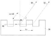
図5は、凹部30の周期間隔を説明するための図である。凹部30の周期間隔とは、2次元の面内において縦または横方向で隣接する凹部の中心間の間隔をいう。周期間隔をLzと、InGaN発光層18からの光の空気中でのピーク波長をλと、その波長λにおけるZnO層24の屈折率をnzλと、ZnO層24と空気層との界面に前記発光層からの光が入射する際の全反射角をθzとする。全反射角θzは、θz=sin−1(1/nzλ)となるので、たとえば波長λ=450nmのときのZnOの屈折率nzλを2.3と、空気の屈折率を1.0とすると、全反射角θzは、約25.8°である。
FIG. 5 is a diagram for explaining the periodic intervals of the
図5において、ZnO層24を横方向に導波する光48から、ZnO層24の法線方向に対してθmの方向に回折される回折光50と回折光52が互いに強め合う条件は、

回折光50と回折光52が互いに強め合う角度θmが全反射角θzより小さいとき、すなわちθmが0≦θm≦θzの範囲にあるとき、互いに強め合う回折光50と回折光52は、ZnO層24と空気との界面で全反射せず、半導体発光素子10の外部に取り出すことができる。つまり、周期間隔Lzが、
また、半導体発光素子では、半導体レーザと違い発光スペクトルがブロードなので、空気中での半値幅Δλを考慮して周期間隔Lzを設定してもよい。すなわち、発光ピーク波長λからΔλだけずれた波長λ±Δλに合わせて周期間隔Lzを設定しても発光効率の改善効果を有する。ここで、半値幅Δλとは、発光ピーク波長λから発光強度が1/2となる波長までの波長幅をいう。半値幅Δλを考慮した場合の周期間隔Lzの範囲は、
さらに、上記のように、回折光50と回折光52が強め合う角度θmが全反射角θzよりも小さい場合に最も望ましいのであるが、実質的には、θmがθzの2倍より小さくても発光効率の改善効果を有する。すなわち、θmが、0≦θm≦2θzの範囲であってもよい。このとき、周期間隔Lzの範囲は、
第1の実施形態においては、ZnO層24の表面に凹部を形成する場合について説明したが、凹部ではなく凸部をZnO層24形成しても同様に光取り出し効率の改善効果を有する。また、上記においては、半導体発光素子10が空気中で発光している場合について説明したが、半導体発光素子10は蛍光体や、光透過性樹脂に覆われた状態であってもよい。この場合は、全反射角θzを求める際に、空気の屈折率ではなく、ZnO層24が接する媒体である蛍光体や光透過性樹脂の屈折率を用いれば、上記の(3)〜(8)式を適用することができる。
In the first embodiment, the case where the concave portion is formed on the surface of the
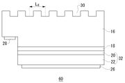
(第2の実施形態)
図6は、本発明の第2の実施形態に係る半導体発光素子の断面図である。図6に示すように、半導体発光素子60は、コンタクト層であるp型GaN22とクラッド層であるp型AlGaN層20とで構成されるp型GaN層32と、InGaN発光層18と、コンタクト層であるn型GaN層16と、が積層されたダブルヘテロ構造のGaN系半導体発光素子である。第2の実施形態に係る半導体発光素子60の発光観測面は、n型GaN層16側である。
(Second Embodiment)
FIG. 6 is a cross-sectional view of a semiconductor light emitting device according to the second embodiment of the present invention. As shown in FIG. 6, the semiconductor
第2の実施形態に係る半導体発光素子60は、まず、サファイア基板上に、n型GaN層16、InGaN発光層18、p型AlGaN層20、p型GaN層22を積層する。ここまでは、第1の実施形態に係る半導体発光素子10と同様の工程であるが、その後、レーザ・リフト・オフによってサファイア基板およびバッファ層を剥離する。レーザとしては、波長248nmのKrFレーザを用いることができる。
In the semiconductor
サファイア基板およびバッファ層剥離によって露出したn型GaN層16の表面には、2次元の周期的な間隔で複数の凹部30が形成される。n型GaN層16の表面とは、InGaN発光層18とn型GaN層16が接している面と対向する面を指す。凹部30は、図2に示すように正方格子状に配置されて形成されてもよい。また、凹部30は、図3に示すように三角格子状に配置されて形成されてもよい。
A plurality of
凹部30の平面視形状は、たとえば図2または図3に示すように円形であってよく、また、四角形や六角形であってもよい。その直径や1辺の長さは100nm程度であってよい。凹部30の深さは、500nm程度であってよい。
The shape of the
凹部30は、第1の実施の形態に係る半導体発光素子10と同様に、RIE法などのドライエッチングを行うことにより形成することができる。n型GaN層16をドライエッチングすることによっても窒素空孔が発生し、n型GaN層16の表面がn型化するが、n型GaN層16は元来n型であるから逆バイアスが印加される状態にはならず、順方向電圧が上昇することはない。
The
凹部30を形成後、p型GaN層22、p型AlGaN層20、InGaN発光層18およびn型GaN層16の一部の領域をエッチングにより除去する。n型GaN層16の途中までエッチングして、露出したn型GaN層16の上面にn側電極28を形成する。
After forming the
その後、p型GaN層22上に、p側電極26を形成する。半導体発光素子60は、発光観測面がn型GaN層16側であるから、p型GaN層22上にZnOの透明電極層は形成する必要はなく、n型GaN層16上に直接p側電極26を形成する。p側電極26は、Pt/Auなどを用いることが望ましい。p側電極26の厚みは、Ptが1000Å程度、Auが3000Å程度であってよい。
Thereafter, the p-
第2の実施形態に係る半導体発光素子60においては、n型GaN層16の表面に2次元の周期的な間隔で凹部が形成されているため、InGaN発光層18からの光が回折される。回折光のうち、n型GaN層16と空気との界面での全反射角θgよりも小さい角度で界面に入射した回折光は、全反射されずに半導体発光素子60の外部に取り出されるため、光取り出し効率を向上させることができる。
In the semiconductor
凹部30の周期間隔Lgは、
(9)式を満たす周期間隔Lgでn型GaN層16の表面に凹部30を形成することによって、回折光を半導体発光素子60の外部に取り出すことができ、光取り出し効率を向上させることができる。たとえば、波長λ=450nm、n型GaN層16の屈折率ngλ=2.5、全反射角θg=23.6°として上記の(9)式を用いて周期間隔Lgを計算すると、180nm≦Lg≦300nmとなる。
By forming the
また、第1の実施形態と同様に、半導体発光素子60の半値幅Δλを考慮して周期間隔Lgを設定しても光取り出し効率を向上させることができる。すなわち、隣接する凹部30の周期間隔Lgが、
さらに、第1の実施形態と同様に、回折光が強め合う角度θmが、0≦θm≦2θgの範囲であっても光取り出し効率を向上させることができる。すなわち、隣接する凹部30の周期間隔Lgが、
図7は、本発明の第2の実施形態に係る半導体発光素子の変形例を示す図である。図7示す半導体発光素子62では、サファイア基板12およびバッファ層14は剥離せずに、ZnO層24側からn型GaN層16の途中までエッチングすることによって露出したn型GaN層16の表面であって、n側電極28を形成する領域以外の場所に、凹部30を形成している。なお、図7においては凹部30の大きさを拡大して描いているため、凹部30は1つしか描かれていないが、実際には複数の凹部30が形成される。
FIG. 7 is a view showing a modification of the semiconductor light emitting device according to the second embodiment of the present invention. In the semiconductor
InGaN発光層18で発光し、バッファ層14とサファイア基板12との界面で反射した光が凹部30を形成した領域に入射した場合、この光は凹部30によって回折されるので、進行方向が変わり、全反射することなく半導体発光素子62の外部に取り出すことができる。半導体発光素子62においても、n型GaN層16に凹部30を形成しているため、n型GaN層16の表面がn型化することによって順方向電圧が上昇することはない。
When the light emitted from the InGaN
第2の実施形態においては、n型GaN層16の表面に凹部を形成する場合について説明したが、凹部ではなく凸部をn型GaN層16の表面に形成しても同様に光取り出し効率の改善効果を有する。また、上記においては、半導体発光素子60または62が空気中で発光している場合について説明したが、半導体発光素子60または62は蛍光体や、光透過性樹脂に覆われた状態であってもよい。この場合は、全反射角θgを求める際に、空気の屈折率ではなく、n型GaN層16が接する媒体である蛍光体や光透過性樹脂の屈折率を用いれば、上記の(9)〜(11)式を適用することができる。
In the second embodiment, the case where the concave portion is formed on the surface of the n-
(第3の実施形態)
図8は、本発明の第3の実施形態に係る半導体発光素子の断面図である。図8に示すように、半導体発光素子70は、SiC基板40上に、コンタクト層であるn型GaN層16と、InGaN発光層18と、クラッド層であるp型AlGaN層20とコンタクト層であるp型GaN22とで構成されるp型GaN層32と、が積層されたダブルヘテロ構造のGaN系半導体発光素子である。半導体発光素子70の発光観測面は、ZnO層24側またはSiC基板40側である。ZnO層24側を発光観測面とする場合には、半導体発光素子70を使用する際に、SiC基板40と実装基板との間にたとえば銀(Ag)からなる反射板(図示せず)を設けるとよい。反射板を設けることで、SiC基板40側から放出された光を発光観測面であるZnO層24側へ反射させることができる。
(Third embodiment)
FIG. 8 is a cross-sectional view of a semiconductor light emitting device according to the third embodiment of the present invention. As shown in FIG. 8, the semiconductor
第3の実施形態に係る半導体発光素子70は、SiC基板40上に、GaN系半導体をエピタキシャル成長させることによって形成し、その後、SiC基板40の表面に凹部30を形成している。ZnO層24上には透明電極として機能するZnO層24を備えるが、ZnO層24に凹部は形成していない。
The semiconductor
SiCはサファイアと異なり導電性であるため、第1または第2の実施形態のようにp型GaN層やInGaN発光層などをエッチングして、n型GaN層16に接続するn側電極を形成する工程は不要であり、製造工程の簡易化と信頼性の向上を図ることができる。
Since SiC is conductive unlike sapphire, the p-type GaN layer, the InGaN light emitting layer, etc. are etched to form the n-side electrode connected to the n-
SiC基板40の表面には、2次元の周期的な間隔で複数の凹部30が形成される。SiC基板40の表面とは、n型GaN層16とSiC基板40が接している面と対向する面を指す。凹部30は、図2に示すように正方格子状に配置されて形成されてもよい。また、凹部30は、図3に示すように三角格子状に配置されて形成されてもよい。
A plurality of
凹部30の平面視形状は、たとえば図2または図3に示すように円形であってよく、また、四角形や六角形であってもよい。その直径や1辺の長さは100nm程度であってよい。凹部30の深さは、500nm程度であってよい。
The shape of the
凹部30は、第1の実施の形態に係る半導体発光素子10と同様に、RIE法などのドライエッチングを行うことにより形成することができる。SiC基板40をドライエッチングしても、プラズマダメージによる順方向電圧の上昇という問題は発生しない。
The
SiC基板40上の凹部30が形成されていない一部の領域には、n側電極28が設けられる。n側電極28は、SiC基板40の表面中央付近に形成することが望ましい。n側電極28は、反射層としても機能し、Ni、Ti、Ni/Ti/Au、またはNiTiアロイなどを用いることができる。n側電極28の厚みは2500Å程度であってよい。
An n-
ZnO層24上の一部の領域には、p側電極26が形成される。基板としてSiC基板40を用いた場合は、p側電極26をZnO層24の表面中央付近に形成することが望ましい。p側電極26は、Pt/Auなどを用いることが望ましい。p側電極26の厚みは、Ptが1000Å程度、Auが3000Å程度であってよい。
A p-
第3の実施形態に係る半導体発光素子70においては、SiC基板40の表面に2次元の周期的な間隔で凹部が形成されているため、InGaN発光層18からSiC基板40方向に放出された光が、SiC基板40と空気との界面で回折される。SiC基板40の法線に対して全反射角θsよりも小さい角度方向に回折された光は、SiC基板40と空気との界面で全反射されることなく半導体発光素子70の外部に取り出すことができ、光取り出し効率を向上させることができる。
In the semiconductor
凹部30の周期間隔Lsは、
(12)式を満たす周期間隔Lsで凹部30を形成することによって、回折光を半導体発光素子70の外部に取り出すことができ、光取り出し効率を向上させることができる。たとえば、波長λ=450nm、SiC基板40の屈折率nsλ=2.65、θs=22.2°として上記の(12)式を用いて周期間隔Lsを計算すると、170nm≦Ls≦273nmとなる。
By forming the
また、半導体発光素子70の半値幅Δλを考慮して周期間隔Lsを設定しても光取り出し効率を向上させることができる。すなわち、隣接する凹部30の周期間隔Lsが、
さらに、回折光が強め合う角度θmが、0≦θm≦2θsの範囲であっても光取り出し効率を向上させることができる。すなわち、隣接する凹部30の周期間隔Lsが、
第3の実施形態においては、SiC基板40の表面に凹部を形成する場合について説明したが、凹部ではなく凸部をSiC基板40の表面に形成しても同様に光取り出し効率の改善効果を有する。また、上記においては、半導体発光素子70が空気中で発光している場合について説明したが、半導体発光素子70は蛍光体や、光透過性樹脂に覆われた状態であってもよい。この場合は、空気ではなく、SiC基板40が接する媒体である蛍光体や光透過性樹脂の屈折率を用いれば、上記の(12)〜(14)式を適用することができる。
In the third embodiment, the case where the concave portion is formed on the surface of the
(第4の実施形態)
図9は、本発明の第4の実施形態に係る半導体発光素子の断面図である。図9に示すように、半導体発光素子80は、SiC基板40上に、コンタクト層であるn型GaN層16と、InGaN発光層18と、クラッド層であるp型AlGaN層20とコンタクト層であるp型GaN22とで構成されるp型GaN層32と、が積層されたダブルヘテロ構造のGaN系半導体発光素子である。第4の実施形態に係る半導体発光素子80の発光観測面は、ZnO層24側またはSiC基板40側である。第3の実施形態と同様に、実装する際には、反射板を設けてもよい。
(Fourth embodiment)
FIG. 9 is a cross-sectional view of a semiconductor light emitting device according to the fourth embodiment of the present invention. As shown in FIG. 9, the semiconductor
第4の実施形態に係る半導体発光素子80は、p型GaN層22上に設けられたZnO層24の表面に凹部38を形成する点が、第3の実施形態に係る半導体発光素子70と異なる。SiC基板40の表面には、第3の実施形態と同様に凹部30が形成される。
The semiconductor
ZnO層24の表面には、2次元の周期的な間隔で複数の凹部38が形成される。ZnO層24の表面とは、ZnO層24とp型GaN層22が接している面と対向する面を指す。凹部38の配置、形状などは、第1の実施形態に係る半導体発光素子10と同様であり、周期間隔Lzは、(3)〜(8)式を適用して設定することができる。ただし、基板としてSiC基板40を用いた場合は、p側電極26をZnO層24の表面中央付近に形成することが望ましい。
A plurality of
第4の実施形態に係る半導体発光素子80では、ZnO層24の表面に2次元の周期的な間隔で凹部38が形成されているため、InGaN発光層18からZnO層24方向に放出された光が回折される。回折光のうち、ZnO層24と空気との界面での全反射角θzよりも小さい角度で界面に入射した回折光は、全反射されずに半導体発光素子80の外部に取り出すことができる。また、SiC基板40の表面に形成した凹部30の効果は、第3の実施形態に係る半導体発光素子70の場合と同様である。
In the semiconductor
第4の実施形態に係る半導体発光素子80においても、第1の実施形態と同様に、p型GaN層22ではなく、ZnO層24に凹部を形成しているため、ドライエッチングの際のプラズマダメージによるp型GaN層22表面のn型化は起こらないので、順方向電圧は上昇しない。また、第3の実施形態と同様に、SiC基板40をドライエッチングしても、プラズマダメージによる順方向電圧の上昇は起こらない。
Also in the semiconductor
(第5の実施形態)
第5の実施形態に係る半導体発光素子は、図1に示す第1の実施形態に係る半導体発光素子10のZnO層24の代わりに、Zn、In、SnおよびMgよりなる群から選択された少なくとも1種の元素を含む酸化物層が、p型GaN層上に形成された半導体発光素子である。第5の実施形態に係る半導体発光素子のその他の構成は、第1の実施形態に係る半導体発光素子10と同様である。
(Fifth embodiment)
The semiconductor light emitting device according to the fifth embodiment is at least selected from the group consisting of Zn, In, Sn, and Mg instead of the
Zn、In、SnおよびMgよりなる群から選択された少なくとも1種の元素を含む酸化物層、すなわち、ITO系酸化物(ITO、In2O3、SnO2、InZnO複合酸化物)層は、マグネトロンスパッタリングにより形成される。ITOのSn含有量は、2〜20%程度であってよい。また、InZnO複合酸化物は、Znの含有量が5〜40%程度であってよい。ITO系酸化物層の厚みが薄すぎると、電流がITO系酸化物層中に拡がらないので、ITO系酸化物層の厚みは、500Å以上とするのが好ましい。ITO系酸化物層の厚みは、厚ければ厚いほど、横方向からの光の取り出しを多くでき、望ましいが、厚く形成する場合はコストがかかるので、10μm以下とするのがよい。 An oxide layer containing at least one element selected from the group consisting of Zn, In, Sn, and Mg, that is, an ITO-based oxide (ITO, In 2 O 3 , SnO 2 , InZnO composite oxide) layer, It is formed by magnetron sputtering. The Sn content of ITO may be about 2 to 20%. The InZnO composite oxide may have a Zn content of about 5 to 40%. If the thickness of the ITO-based oxide layer is too thin, the current does not spread into the ITO-based oxide layer. Therefore, the thickness of the ITO-based oxide layer is preferably 500 mm or more. The thicker the ITO-based oxide layer, the more light can be taken out from the lateral direction, and it is desirable. However, since the thickness of the ITO-based oxide layer is high, it is preferable that the thickness be 10 μm or less.
p型GaNは、プラズマダメージに弱いため、ダメージが入らないようにスパッタリングの条件を調整する必要がある。たとえば、4インチの大きさのターゲットであれば、投入するスパッタパワーは、600W以下であることが望ましい。ITO系酸化物層は、GaN系半導体発光素子の発光波長帯に対して透過率が高く、透明導電膜層として機能する。 Since p-type GaN is vulnerable to plasma damage, it is necessary to adjust the sputtering conditions so as not to cause damage. For example, if the target has a size of 4 inches, it is desirable that the sputtering power to be input is 600 W or less. The ITO-based oxide layer has a high transmittance with respect to the emission wavelength band of the GaN-based semiconductor light-emitting element, and functions as a transparent conductive film layer.
プラズマダメージをより効果的に避ける場合には、真空蒸着法を用いて蒸着する方法をとることもできる。また、真空蒸着法を行った後にマグネトロンスパッタリング法を行う2段階の製膜を行ってもよい。この場合、真空蒸着法を単独で用いた場合よりも、透明度の高い電極層を形成することができる。 In order to avoid plasma damage more effectively, a method of vapor deposition using a vacuum vapor deposition method can be employed. Alternatively, two-stage film formation may be performed in which the magnetron sputtering method is performed after the vacuum deposition method is performed. In this case, an electrode layer with higher transparency can be formed than when the vacuum deposition method is used alone.
ITO系酸化物層の表面には、2次元の周期的な間隔で凹部または凸部が形成される。ITO系酸化物層の表面とは、ITO系酸化物層とp型GaN層が接している面と対向する面を指す。凹部または凸部の配置、形状などは、第1の実施形態に係る半導体発光素子10と同様であり、周期間隔Lzは、(3)〜(8)式を適用して設定することができる。なお、(3)〜(8)式を適用する場合、ZnO層の屈折率nzλは、ITO系酸化物層の屈折率nIλに置き換え、ZnO層と空気層との界面に前記発光層からの光が入射する際の全反射角θzは、ITO系酸化物層と空気層との界面に発光層からの光が入射する際の全反射角θIに置き換えて適用する。
Concave portions or convex portions are formed on the surface of the ITO-based oxide layer at two-dimensional periodic intervals. The surface of the ITO-based oxide layer refers to the surface facing the surface where the ITO-based oxide layer and the p-type GaN layer are in contact. The arrangement, shape, and the like of the recesses or protrusions are the same as those of the semiconductor
第5の実施形態に係る半導体発光素子では、透明導電膜層として機能するITO系酸化物層の表面に、2次元の周期的な間隔で凹部または凸部が形成されているため、InGaN発光層からITO系酸化物層方向に放出された光が回折される。回折光のうち、ITO系酸化物層と空気との界面での全反射角θIよりも小さい角度で界面に入射した回折光は、全反射されずに半導体発光素子の外部に取り出すことができる。 In the semiconductor light emitting device according to the fifth embodiment, since the concave or convex portions are formed at two-dimensional periodic intervals on the surface of the ITO-based oxide layer functioning as the transparent conductive film layer, the InGaN light emitting layer The light emitted from the direction toward the ITO-based oxide layer is diffracted. Of the diffracted light, diffracted light incident on the interface at an angle smaller than the total reflection angle θ I at the interface between the ITO-based oxide layer and air can be extracted outside the semiconductor light emitting element without being totally reflected. .
第5の実施形態に係る半導体発光素子においても、第1の実施形態と同様に、p型GaN層ではなく、ITO系酸化物層に凹部を形成しているため、ドライエッチングの際のプラズマダメージによるp型GaN層表面のn型化は起こらないので、順方向電圧は上昇しない。また、従来必要であったドライエッチング後のウェットエッチングの工程が不要となるので、製造コストを削減することができる。 In the semiconductor light emitting device according to the fifth embodiment, as in the first embodiment, since the recess is formed in the ITO-based oxide layer instead of the p-type GaN layer, plasma damage during dry etching is caused. Since the n-type surface of the p-type GaN layer does not occur, the forward voltage does not increase. In addition, since the wet etching process after dry etching, which has been conventionally required, becomes unnecessary, the manufacturing cost can be reduced.
ITO系酸化物は、ZnOのようにGaNと同じ結晶構造をとるわけではないものの、p−GaNに対してオーミック電極として用いることができる。ZnOの比抵抗率は、約2×10⁻⁴Ωcm程度であるのに対し、ITO系酸化物の比抵抗率は、約9×10⁻⁵〜1×10⁻⁴Ωcm程度である。これは、ITO系酸化物がZnOよりも電流が拡がり易いことを意味するので、ITO系酸化物層をp型GaN層上に形成した場合には、ZnO層を形成する場合よりも膜厚を薄くすることができる。 Although the ITO-based oxide does not have the same crystal structure as GaN like ZnO, it can be used as an ohmic electrode for p-GaN. The specific resistivity of ZnO is about 2 × 10 −4 Ωcm, whereas the specific resistivity of ITO-based oxide is about 9 × 10 −5 to 1 × 10 −4 Ωcm. This means that the current of the ITO-based oxide is easier to spread than that of ZnO. Therefore, when the ITO-based oxide layer is formed on the p-type GaN layer, the film thickness is larger than when the ZnO layer is formed. Can be thinned.
(第6の実施形態)
第6の実施形態に係る半導体発光素子は、図9に示す第4の実施形態に係る半導体発光素子80のZnO層24の代わりに、Zn、In、SnおよびMgよりなる群から選択された少なくとも1種の元素を含む酸化物層が、p型GaN層上に形成された半導体発光素子である。第6の実施形態に係る半導体発光素子のその他の構成は、第4の実施形態に係る半導体発光素子80と同様である。
(Sixth embodiment)
The semiconductor light emitting device according to the sixth embodiment is at least selected from the group consisting of Zn, In, Sn and Mg instead of the
Zn、In、SnおよびMgよりなる群から選択された少なくとも1種の元素を含む酸化物層、すなわち、ITO系酸化物(ITO、In2O3、SnO2、InZnO複合酸化物)層の形成方法、厚み等は、第5の実施形態に係る半導体発光素子と同様であってよい。SiC基板の表面には、第3、第4の実施形態と同様に凹部または凸部が形成される。 Formation of an oxide layer containing at least one element selected from the group consisting of Zn, In, Sn, and Mg, that is, an ITO-based oxide (ITO, In 2 O 3 , SnO 2 , InZnO composite oxide) layer The method, thickness, and the like may be the same as those of the semiconductor light emitting device according to the fifth embodiment. A concave portion or a convex portion is formed on the surface of the SiC substrate as in the third and fourth embodiments.
ITO系酸化物層の表面には、2次元の周期的な間隔で凹部または凸部が形成される。ITO系酸化物層の表面とは、ITO系酸化物層とp型GaN層が接している面と対向する面を指す。凹部または凸部の配置、形状などは、第1の実施形態に係る半導体発光素子10と同様であり、周期間隔Lzは、(3)〜(8)式を適用して設定することができる。なお、(3)〜(8)式を適用する場合、ZnO層の屈折率nzλは、ITO系酸化物層の屈折率nIλに置き換え、ZnO層と空気層との界面に前記発光層からの光が入射する際の全反射角θzは、ITO系酸化物層と空気層との界面に発光層からの光が入射する際の全反射角θIに置き換えて適用する。
Concave portions or convex portions are formed on the surface of the ITO-based oxide layer at two-dimensional periodic intervals. The surface of the ITO-based oxide layer refers to the surface facing the surface where the ITO-based oxide layer and the p-type GaN layer are in contact. The arrangement, shape, and the like of the recesses or protrusions are the same as those of the semiconductor
第6の実施形態に係る半導体発光素子では、透明導電膜層として機能するITO系酸化物層の表面に、2次元の周期的な間隔で凹部または凸部が形成されているため、InGaN発光層からITO系酸化物層方向に放出された光が回折される。回折光のうち、ITO系酸化物層と空気との界面での全反射角θIよりも小さい角度で界面に入射した回折光は、全反射されずに半導体発光素子の外部に取り出すことができる。また、SiC基板の表面に形成した凹部または凸部の効果は、第3、第4の実施形態に係る半導体発光素子の場合と同様である。 In the semiconductor light emitting device according to the sixth embodiment, since recesses or projections are formed at two-dimensional periodic intervals on the surface of the ITO-based oxide layer functioning as a transparent conductive film layer, an InGaN light emitting layer The light emitted from the direction toward the ITO-based oxide layer is diffracted. Of the diffracted light, diffracted light incident on the interface at an angle smaller than the total reflection angle θ I at the interface between the ITO-based oxide layer and air can be extracted outside the semiconductor light emitting element without being totally reflected. . Moreover, the effect of the recessed part or convex part formed in the surface of a SiC substrate is the same as that of the case of the semiconductor light-emitting device which concerns on 3rd, 4th embodiment.
第6の実施形態に係る半導体発光素子においても、第1の実施形態と同様に、p型GaN層ではなく、ITO系酸化物層に凹部を形成しているため、ドライエッチングの際のプラズマダメージによるp型GaN層表面のn型化は起こらないので、順方向電圧は上昇しない。また、第5の実施形態と同様に、ZnO層を形成する場合よりも、ITO系酸化膜の膜厚を薄くすることができる。また、従来必要であったドライエッチング後のウェットエッチングの工程が不要となるので、製造コストを削減することができる。 Also in the semiconductor light emitting device according to the sixth embodiment, as in the first embodiment, since the recess is formed in the ITO-based oxide layer instead of the p-type GaN layer, plasma damage during dry etching is caused. Since the n-type surface of the p-type GaN layer does not occur, the forward voltage does not increase. Further, as in the fifth embodiment, the ITO-based oxide film can be made thinner than when the ZnO layer is formed. In addition, since the wet etching process after dry etching, which has been conventionally required, becomes unnecessary, the manufacturing cost can be reduced.
以上、本発明を実施の形態をもとに説明した。この実施の形態は例示であり、それらの各構成要素や各処理プロセスの組み合わせにいろいろな変形例が可能なこと、またそうした変形例も本発明の範囲にあることは、当業者に理解されるところである。 The present invention has been described based on the embodiments. This embodiment is an exemplification, and it is understood by those skilled in the art that various modifications can be made to the combination of each component and each processing process, and such modifications are also within the scope of the present invention. By the way.
第5および第6の実施形態では、p型GaN層上にITO系酸化物層を形成したが、p型GaN層上に、ITO系酸化物層とMgxZn1−xO層(0≦x≦0.5)とを積層した透明導電膜層を形成し、この透明導電膜層に対して2次元の周期的な間隔で凹部または凸部を形成してもよい。この場合も、第5および第6の実施形態と同様に、光の取り出し効率を向上させることができる。 In the fifth and sixth embodiments, the ITO-based oxide layer is formed on the p-type GaN layer, but the ITO-based oxide layer and the Mg x Zn 1-x O layer (0 ≦ 0) are formed on the p-type GaN layer. x ≦ 0.5) may be formed, and concave portions or convex portions may be formed at two-dimensional periodic intervals with respect to the transparent conductive layer. Also in this case, the light extraction efficiency can be improved as in the fifth and sixth embodiments.
ITO系酸化物層とMgxZn1−xO層(0≦x≦0.5)の積層順序は、どちらもオーミックコンタクトを取れるので、p型GaN層、MgxZn1−xO層(0≦x≦0.5)、ITO系酸化物層の順序で積層してもよいし、p型GaN層、ITO系酸化物層、MgxZn1−xO層(0≦x≦0.5)の順序で積層してもよい。p型GaN層、MgxZn1−xO層(0≦x≦0.5)、ITO系酸化物層の順序で積層した場合、GaNとMgxZn1−xO層(0≦x≦0.5)の結晶は、同じウルツァイト構造をとるため、良好な接合界面を得ることができる。 Since both the ITO-based oxide layer and the Mg x Zn 1-x O layer (0 ≦ x ≦ 0.5) are in ohmic contact, the p-type GaN layer, the Mg x Zn 1-x O layer ( 0 ≦ x ≦ 0.5), an ITO-based oxide layer may be laminated in this order, or a p-type GaN layer, an ITO-based oxide layer, and an Mg x Zn 1-x O layer (0 ≦ x ≦ 0. You may laminate in the order of 5). When the p-type GaN layer, the Mg x Zn 1-x O layer (0 ≦ x ≦ 0.5), and the ITO-based oxide layer are stacked in this order, GaN and Mg x Zn 1-x O layer (0 ≦ x ≦ Since the crystal of 0.5) has the same wurtzite structure, a good bonding interface can be obtained.
また、p型GaN層、ITO系酸化物層、MgxZn1−xO層(0≦x≦0.5)の順序で積層した場合、2次元構造プロセスが簡単になるというメリットがある。MgxZn1−xO層(0≦x≦0.5)が酸、特にHClに溶けやすく、それに比べるとITO系酸化物ははるかにHClで溶けにくい。従って、MgxZn1−xO層(0≦x≦0.5)上に2次元パターンを作り、ウェットエッチングすれば、ITO系酸化物が擬似的にエッチングストップ層となり、所望の2次元構造を容易に作ることができる。 Further, when the p-type GaN layer, the ITO-based oxide layer, and the Mg x Zn 1-x O layer (0 ≦ x ≦ 0.5) are stacked in this order, there is an advantage that the two-dimensional structure process is simplified. The Mg x Zn 1-x O layer (0 ≦ x ≦ 0.5) is easily dissolved in acid, particularly HCl, and the ITO-based oxide is much less soluble in HCl than that. Accordingly, if a two-dimensional pattern is formed on the Mg x Zn 1-x O layer (0 ≦ x ≦ 0.5) and wet etching is performed, the ITO-based oxide becomes a pseudo etching stop layer, and a desired two-dimensional structure is obtained. Can be made easily.
上記の実施形態においては、第1〜第4の実施形態ではZnO層またはMgxZn1−xO層(0≦x≦0.5)が、第5〜第6の実施形態ではITO系酸化物層が、電流拡がり層としての機能を有している。GaN系半導体発光素子では、電流拡がり層は必須である。電流拡がり層が存在しない場合、半導体側のコンタクト層であるp型GaNは数Ωcmと比抵抗が非常に高いため、赤色半導体発光素子のようにコンタクト層に100μm径のパッド電極をつけただけでは活性層全体に電流が行き渡らず、殆どパッド電極直下しか発光しない。300μm角のチップで考えると、チップ全体に電流が拡がるためのp型GaN層の厚みは、数mmというオーダーになり、現実的ではない。従って、GaN系半導体発光素子では、p型GaN層の手前で電流を拡げる必要があり、第1〜第4の実施形態ではZnO層またはMgxZn1−xO層(0≦x≦0.5)が、第5〜第6の実施形態ではITO系酸化物層がその役割を果たす。そのため、図1に示すように、凹部または凸部を形成した場合であっても、半導体層の直上ではZnO層、MgxZn1−xO層(0≦x≦0.5)、ITO系酸化物層が連続的につながっていることが好ましい。凹部または凸部を形成した後の膜厚が薄くなった部分の厚みは、駆動電流にもよるが、500Å程度残しておくことが好ましい。膜厚が薄くなった部分の厚みを500Å程度残しておくことにより、電流拡がり層として効果的に機能することができる。 In the above embodiment, the ZnO layer or the Mg x Zn 1-x O layer (0 ≦ x ≦ 0.5) is used in the first to fourth embodiments, and the ITO-based oxidation is used in the fifth to sixth embodiments. The physical layer has a function as a current spreading layer. In the GaN-based semiconductor light emitting device, the current spreading layer is essential. When there is no current spreading layer, p-type GaN, which is a contact layer on the semiconductor side, has a very high specific resistance of several Ωcm. Therefore, just by attaching a 100 μm diameter pad electrode to the contact layer like a red semiconductor light emitting device. Current does not reach the entire active layer, and light is emitted almost directly below the pad electrode. Considering a 300 μm square chip, the thickness of the p-type GaN layer for spreading the current over the entire chip is on the order of several mm, which is not realistic. Therefore, in the GaN-based semiconductor light emitting device, it is necessary to spread the current before the p-type GaN layer. In the first to fourth embodiments, the ZnO layer or the Mg x Zn 1-x O layer (0 ≦ x ≦ 0. 5) However, the ITO-based oxide layer plays a role in the fifth to sixth embodiments. Therefore, as shown in FIG. 1, even when a recess or a protrusion is formed, a ZnO layer, a Mg x Zn 1-x O layer (0 ≦ x ≦ 0.5), an ITO-based layer is formed immediately above the semiconductor layer. The oxide layers are preferably connected continuously. The thickness of the thinned portion after forming the concave portion or the convex portion is preferably about 500 mm, although it depends on the driving current. By leaving about 500 mm of the thickness of the thinned portion, it can effectively function as a current spreading layer.
10 半導体発光素子、 12 サファイア基板、 14 バッファ層、 16 n型GaN層、 18 InGaN発光層、 24 ZnO層、 26 p側電極、 28 n側電極、 30 凹部、 32 p型GaN層。 10 semiconductor light emitting device, 12 sapphire substrate, 14 buffer layer, 16 n-type GaN layer, 18 InGaN light emitting layer, 24 ZnO layer, 26 p-side electrode, 28 n-side electrode, 30 recess, 32 p-type GaN layer.
Claims (17)
前記p型GaN層上にMgxZn1−xO層(0≦x≦0.5)が設けられ、
前記MgxZn1−xO層(0≦x≦0.5)の表面に、2次元の周期的な間隔で凹部または凸部が形成されることを特徴とする半導体発光素子。 A semiconductor light-emitting device in which an n-type GaN layer, a light-emitting layer, and a p-type GaN layer are stacked on a substrate,
An Mg x Zn 1-x O layer (0 ≦ x ≦ 0.5) is provided on the p-type GaN layer,
A semiconductor light emitting device, wherein concave portions or convex portions are formed at two-dimensional periodic intervals on the surface of the Mg x Zn 1-x O layer (0 ≦ x ≦ 0.5).
前記n型GaN層の表面に、2次元の周期的な間隔で凹部または凸部が形成されることを特徴とする半導体発光素子。 A semiconductor light-emitting device in which a p-type GaN layer, a light-emitting layer, and an n-type GaN layer are stacked,
A semiconductor light emitting device, wherein recesses or projections are formed on the surface of the n-type GaN layer at two-dimensional periodic intervals.
前記基板は、SiC基板であり、
前記SiC基板の表面に、2次元の周期的な間隔で凹部または凸部が形成され、
前記p型GaN層上にMgxZn1−xO層(0≦x≦0.5)が設けられ、
前記MgxZn1−xO層(0≦x≦0.5)の表面に、2次元の周期的な間隔で凹部または凸部が形成されることを特徴とする半導体発光素子。 A semiconductor light-emitting device in which an n-type GaN layer, a light-emitting layer, and a p-type GaN layer are stacked on a substrate,
The substrate is a SiC substrate;
Concave portions or convex portions are formed on the surface of the SiC substrate at two-dimensional periodic intervals,
An Mg x Zn 1-x O layer (0 ≦ x ≦ 0.5) is provided on the p-type GaN layer,
A semiconductor light emitting device, wherein concave portions or convex portions are formed at two-dimensional periodic intervals on the surface of the Mg x Zn 1-x O layer (0 ≦ x ≦ 0.5).
前記p型GaN層上に、Zn、In、SnおよびMgよりなる群から選択された少なくとも1種の元素を含む酸化物層よりなる透明導電膜層、もしくはその酸化物層とMgxZn1−xO層(0≦x≦0.5)とを積層した透明導電膜層が設けられ、
前記透明導電膜層の表面に、2次元の周期的な間隔で凹部または凸部が形成されることを特徴とする半導体発光素子。 A semiconductor light-emitting device in which an n-type GaN layer, a light-emitting layer, and a p-type GaN layer are stacked on a substrate,
On the p-type GaN layer, a transparent conductive film layer made of an oxide layer containing at least one element selected from the group consisting of Zn, In, Sn and Mg, or the oxide layer and Mg x Zn 1− x O layer (0 ≦ x ≦ 0.5) and a transparent conductive film layer formed by laminating is provided,
A semiconductor light emitting device, wherein concave portions or convex portions are formed on the surface of the transparent conductive film layer at two-dimensional periodic intervals.
前記基板は、SiC基板であり、
前記SiC基板の表面に、2次元の周期的な間隔で凹部または凸部が形成され、
前記p型GaN層上に、Zn、In、SnおよびMgよりなる群から選択された少なくとも1種の元素を含む酸化物層よりなる透明導電膜層、もしくはその酸化物層とMgxZn1−xO層(0≦x≦0.5)とを積層した透明導電膜層が設けられ、
前記透明導電膜層の表面に、2次元の周期的な間隔で凹部または凸部が形成されることを特徴とする半導体発光素子。 A semiconductor light-emitting device in which an n-type GaN layer, a light-emitting layer, and a p-type GaN layer are stacked on a substrate,
The substrate is a SiC substrate;
Concave portions or convex portions are formed on the surface of the SiC substrate at two-dimensional periodic intervals,
On the p-type GaN layer, a transparent conductive film layer made of an oxide layer containing at least one element selected from the group consisting of Zn, In, Sn and Mg, or the oxide layer and Mg x Zn 1− x O layer (0 ≦ x ≦ 0.5) and a transparent conductive film layer formed by laminating is provided,
A semiconductor light emitting device, wherein concave portions or convex portions are formed on the surface of the transparent conductive film layer at two-dimensional periodic intervals.
Priority Applications (1)
| Application Number | Priority Date | Filing Date | Title |
|---|---|---|---|
| JP2006159459A JP2007019488A (en) | 2005-06-09 | 2006-06-08 | Semiconductor light emitting element |
Applications Claiming Priority (2)
| Application Number | Priority Date | Filing Date | Title |
|---|---|---|---|
| JP2005169056 | 2005-06-09 | ||
| JP2006159459A JP2007019488A (en) | 2005-06-09 | 2006-06-08 | Semiconductor light emitting element |
Publications (1)
| Publication Number | Publication Date |
|---|---|
| JP2007019488A true JP2007019488A (en) | 2007-01-25 |
Family
ID=37756327
Family Applications (1)
| Application Number | Title | Priority Date | Filing Date |
|---|---|---|---|
| JP2006159459A Pending JP2007019488A (en) | 2005-06-09 | 2006-06-08 | Semiconductor light emitting element |
Country Status (1)
| Country | Link |
|---|---|
| JP (1) | JP2007019488A (en) |
Cited By (15)
| Publication number | Priority date | Publication date | Assignee | Title |
|---|---|---|---|---|
| JP2007123517A (en) * | 2005-10-27 | 2007-05-17 | Toshiba Corp | Semiconductor light-emitting element, and semiconductor light-emitting apparatus |
| KR100767258B1 (en) | 2007-05-15 | 2007-10-17 | 주식회사 시스넥스 | Nitride semiconductor light emitting device and manufacturing method thereof |
| JP2008226962A (en) * | 2007-03-09 | 2008-09-25 | Sumitomo Chemical Co Ltd | Semiconductor light-emitting element and manufacturing method therefor |
| JP2009054889A (en) * | 2007-08-28 | 2009-03-12 | Yamaguchi Univ | Ito electrode, its manufacturing method, and nitride semiconductor light-emitting element |
| JP2010114411A (en) * | 2008-11-06 | 2010-05-20 | Samsung Electro-Mechanics Co Ltd | Compound semiconductor light emitting element, and method for manufacturing the same |
| JP2010287761A (en) * | 2009-06-12 | 2010-12-24 | Showa Denko Kk | Semiconductor light-emitting element, method of manufacturing semiconductor light-emitting element, lamp with semiconductor light-emitting element, lighting device, and electronic equipment |
| KR101047739B1 (en) * | 2010-04-28 | 2011-07-07 | 엘지이노텍 주식회사 | Light emitting device, method for fabricating the same, light emitting device package and lighting system including the same |
| US8026155B2 (en) | 2009-02-04 | 2011-09-27 | Empire Technology Development Llc | Method for producing semiconductor device |
| US8188496B2 (en) | 2008-11-06 | 2012-05-29 | Samsung Led Co., Ltd. | Semiconductor light emitting device including substrate having protection layers and method for manufacturing the same |
| JP2014082401A (en) * | 2012-10-18 | 2014-05-08 | Ushio Inc | Fluorescent light source device |
| JP2014170977A (en) * | 2014-06-27 | 2014-09-18 | Toshiba Corp | Light-emitting device |
| US9243778B2 (en) | 2013-05-31 | 2016-01-26 | Panasonic Intellectual Property Management Co., Ltd. | Wavelength conversion element, light emitting device including wavelength conversion element, and vehicle including light emitting device |
| JPWO2014119783A1 (en) * | 2013-02-04 | 2017-01-26 | ウシオ電機株式会社 | Fluorescent light source device |
| JP2019071473A (en) * | 2019-01-15 | 2019-05-09 | 信越半導体株式会社 | Light emitting element |
| WO2020067235A1 (en) * | 2018-09-26 | 2020-04-02 | 出光興産株式会社 | Oxide multilayer body and method for producing same |
Citations (4)
| Publication number | Priority date | Publication date | Assignee | Title |
|---|---|---|---|---|
| JP2000196152A (en) * | 1998-12-24 | 2000-07-14 | Toshiba Corp | Semiconductor light emitting device and manufacture thereof |
| JP2002164570A (en) * | 2000-11-24 | 2002-06-07 | Shiro Sakai | Gallium nitride compound semiconductor device |
| JP2004266258A (en) * | 2003-02-12 | 2004-09-24 | Rohm Co Ltd | Semiconductor light emitting device |
| JP2005005679A (en) * | 2003-04-15 | 2005-01-06 | Matsushita Electric Ind Co Ltd | Semiconductor light emitting device and its manufacturing method |
-
2006
- 2006-06-08 JP JP2006159459A patent/JP2007019488A/en active Pending
Patent Citations (4)
| Publication number | Priority date | Publication date | Assignee | Title |
|---|---|---|---|---|
| JP2000196152A (en) * | 1998-12-24 | 2000-07-14 | Toshiba Corp | Semiconductor light emitting device and manufacture thereof |
| JP2002164570A (en) * | 2000-11-24 | 2002-06-07 | Shiro Sakai | Gallium nitride compound semiconductor device |
| JP2004266258A (en) * | 2003-02-12 | 2004-09-24 | Rohm Co Ltd | Semiconductor light emitting device |
| JP2005005679A (en) * | 2003-04-15 | 2005-01-06 | Matsushita Electric Ind Co Ltd | Semiconductor light emitting device and its manufacturing method |
Cited By (19)
| Publication number | Priority date | Publication date | Assignee | Title |
|---|---|---|---|---|
| JP2007123517A (en) * | 2005-10-27 | 2007-05-17 | Toshiba Corp | Semiconductor light-emitting element, and semiconductor light-emitting apparatus |
| JP2008226962A (en) * | 2007-03-09 | 2008-09-25 | Sumitomo Chemical Co Ltd | Semiconductor light-emitting element and manufacturing method therefor |
| KR100767258B1 (en) | 2007-05-15 | 2007-10-17 | 주식회사 시스넥스 | Nitride semiconductor light emitting device and manufacturing method thereof |
| JP2009054889A (en) * | 2007-08-28 | 2009-03-12 | Yamaguchi Univ | Ito electrode, its manufacturing method, and nitride semiconductor light-emitting element |
| US8188496B2 (en) | 2008-11-06 | 2012-05-29 | Samsung Led Co., Ltd. | Semiconductor light emitting device including substrate having protection layers and method for manufacturing the same |
| US8916402B2 (en) | 2008-11-06 | 2014-12-23 | Samsung Electronics Co., Ltd. | Semiconductor light emitting device including substrate having protection layers providing protection against chemicals and method for manufacturing the same |
| JP2010114411A (en) * | 2008-11-06 | 2010-05-20 | Samsung Electro-Mechanics Co Ltd | Compound semiconductor light emitting element, and method for manufacturing the same |
| US8026155B2 (en) | 2009-02-04 | 2011-09-27 | Empire Technology Development Llc | Method for producing semiconductor device |
| JP2010287761A (en) * | 2009-06-12 | 2010-12-24 | Showa Denko Kk | Semiconductor light-emitting element, method of manufacturing semiconductor light-emitting element, lamp with semiconductor light-emitting element, lighting device, and electronic equipment |
| KR101047739B1 (en) * | 2010-04-28 | 2011-07-07 | 엘지이노텍 주식회사 | Light emitting device, method for fabricating the same, light emitting device package and lighting system including the same |
| US8507942B2 (en) | 2010-04-28 | 2013-08-13 | Lg Innotek Co., Ltd. | Light emitting device, light emitting device package and lighting system |
| JP2014082401A (en) * | 2012-10-18 | 2014-05-08 | Ushio Inc | Fluorescent light source device |
| JPWO2014119783A1 (en) * | 2013-02-04 | 2017-01-26 | ウシオ電機株式会社 | Fluorescent light source device |
| US9243778B2 (en) | 2013-05-31 | 2016-01-26 | Panasonic Intellectual Property Management Co., Ltd. | Wavelength conversion element, light emitting device including wavelength conversion element, and vehicle including light emitting device |
| JP2014170977A (en) * | 2014-06-27 | 2014-09-18 | Toshiba Corp | Light-emitting device |
| WO2020067235A1 (en) * | 2018-09-26 | 2020-04-02 | 出光興産株式会社 | Oxide multilayer body and method for producing same |
| JPWO2020067235A1 (en) * | 2018-09-26 | 2021-10-14 | 出光興産株式会社 | Oxide laminate and its manufacturing method |
| JP7357883B2 (en) | 2018-09-26 | 2023-10-10 | 出光興産株式会社 | Oxide laminate and method for manufacturing the same |
| JP2019071473A (en) * | 2019-01-15 | 2019-05-09 | 信越半導体株式会社 | Light emitting element |
Similar Documents
| Publication | Publication Date | Title |
|---|---|---|
| US7906791B2 (en) | Semiconductor light emitting element | |
| JP2007019488A (en) | Semiconductor light emitting element | |
| JP5391469B2 (en) | Nitride semiconductor light emitting device and manufacturing method thereof | |
| JP5719110B2 (en) | Light emitting element | |
| JP2011119519A (en) | Semiconductor light emitting element and semiconductor light emitting device | |
| KR20080003901A (en) | Nitride semiconductor light emitting element | |
| KR20080087135A (en) | Nitride semiconductor light emitting element | |
| JP2005116794A (en) | Nitride semiconductor light emitting element | |
| KR101337616B1 (en) | Fabrication method of light emitting device having scattering center laminated with a plurality of insulator layer and light emitting device thereby | |
| JP2011066073A (en) | Semiconductor light-emitting element | |
| JP2005268601A (en) | Compound semiconductor light-emitting device | |
| JP2007258277A (en) | Semiconductor light emitting device | |
| JP2005354049A (en) | Semiconductor laser device | |
| JP5116291B2 (en) | LIGHT EMITTING ELEMENT AND LIGHTING DEVICE | |
| JP2008159894A (en) | Light emitting element and illuminator | |
| US20120080707A1 (en) | Semiconductor light emitting device and manufacturing method thereof | |
| KR20080058722A (en) | Fabrication method of light emitting device having scattering center laminated with a plurality of insulator layer and light emitting device thereby | |
| JP2012253074A (en) | Nitride based light-emitting diode element | |
| KR20110093006A (en) | Nitride light emitting device | |
| KR101154511B1 (en) | High efficiency light emitting diode and method of fabricating the same | |
| KR101616905B1 (en) | Semiconductor light-emitting device | |
| KR20170038439A (en) | Light emitting device | |
| KR20170095675A (en) | Light emitting device | |
| KR100998013B1 (en) | Semiconductor light emitting device | |
| JP2007250714A (en) | Light emitting element |
Legal Events
| Date | Code | Title | Description |
|---|---|---|---|
| A621 | Written request for application examination |
Free format text: JAPANESE INTERMEDIATE CODE: A621 Effective date: 20090520 |
|
| A977 | Report on retrieval |
Free format text: JAPANESE INTERMEDIATE CODE: A971007 Effective date: 20110622 |
|
| A131 | Notification of reasons for refusal |
Free format text: JAPANESE INTERMEDIATE CODE: A131 Effective date: 20110628 |
|
| A521 | Written amendment |
Free format text: JAPANESE INTERMEDIATE CODE: A523 Effective date: 20110823 |
|
| A02 | Decision of refusal |
Free format text: JAPANESE INTERMEDIATE CODE: A02 Effective date: 20120410 |