JP2007013092A - Method for manufacturing wiring substrate and semiconductor device - Google Patents
Method for manufacturing wiring substrate and semiconductor device Download PDFInfo
- Publication number
- JP2007013092A JP2007013092A JP2006014199A JP2006014199A JP2007013092A JP 2007013092 A JP2007013092 A JP 2007013092A JP 2006014199 A JP2006014199 A JP 2006014199A JP 2006014199 A JP2006014199 A JP 2006014199A JP 2007013092 A JP2007013092 A JP 2007013092A
- Authority
- JP
- Japan
- Prior art keywords
- electrode
- manufacturing
- support substrate
- opening
- wiring board
- Prior art date
- Legal status (The legal status is an assumption and is not a legal conclusion. Google has not performed a legal analysis and makes no representation as to the accuracy of the status listed.)
- Granted
Links
Images


Classifications
-
- H—ELECTRICITY
- H05—ELECTRIC TECHNIQUES NOT OTHERWISE PROVIDED FOR
- H05K—PRINTED CIRCUITS; CASINGS OR CONSTRUCTIONAL DETAILS OF ELECTRIC APPARATUS; MANUFACTURE OF ASSEMBLAGES OF ELECTRICAL COMPONENTS
- H05K1/00—Printed circuits
- H05K1/02—Details
- H05K1/11—Printed elements for providing electric connections to or between printed circuits
- H05K1/115—Via connections; Lands around holes or via connections
-
- H—ELECTRICITY
- H01—ELECTRIC ELEMENTS
- H01L—SEMICONDUCTOR DEVICES NOT COVERED BY CLASS H10
- H01L21/00—Processes or apparatus adapted for the manufacture or treatment of semiconductor or solid state devices or of parts thereof
- H01L21/02—Manufacture or treatment of semiconductor devices or of parts thereof
- H01L21/04—Manufacture or treatment of semiconductor devices or of parts thereof the devices having at least one potential-jump barrier or surface barrier, e.g. PN junction, depletion layer or carrier concentration layer
- H01L21/18—Manufacture or treatment of semiconductor devices or of parts thereof the devices having at least one potential-jump barrier or surface barrier, e.g. PN junction, depletion layer or carrier concentration layer the devices having semiconductor bodies comprising elements of Group IV of the Periodic System or AIIIBV compounds with or without impurities, e.g. doping materials
- H01L21/28—Manufacture of electrodes on semiconductor bodies using processes or apparatus not provided for in groups H01L21/20 - H01L21/268
-
- H—ELECTRICITY
- H01—ELECTRIC ELEMENTS
- H01L—SEMICONDUCTOR DEVICES NOT COVERED BY CLASS H10
- H01L21/00—Processes or apparatus adapted for the manufacture or treatment of semiconductor or solid state devices or of parts thereof
- H01L21/02—Manufacture or treatment of semiconductor devices or of parts thereof
- H01L21/04—Manufacture or treatment of semiconductor devices or of parts thereof the devices having at least one potential-jump barrier or surface barrier, e.g. PN junction, depletion layer or carrier concentration layer
- H01L21/48—Manufacture or treatment of parts, e.g. containers, prior to assembly of the devices, using processes not provided for in a single one of the subgroups H01L21/06 - H01L21/326
- H01L21/4814—Conductive parts
- H01L21/4846—Leads on or in insulating or insulated substrates, e.g. metallisation
- H01L21/4857—Multilayer substrates
-
- H—ELECTRICITY
- H01—ELECTRIC ELEMENTS
- H01L—SEMICONDUCTOR DEVICES NOT COVERED BY CLASS H10
- H01L21/00—Processes or apparatus adapted for the manufacture or treatment of semiconductor or solid state devices or of parts thereof
- H01L21/67—Apparatus specially adapted for handling semiconductor or electric solid state devices during manufacture or treatment thereof; Apparatus specially adapted for handling wafers during manufacture or treatment of semiconductor or electric solid state devices or components ; Apparatus not specifically provided for elsewhere
- H01L21/683—Apparatus specially adapted for handling semiconductor or electric solid state devices during manufacture or treatment thereof; Apparatus specially adapted for handling wafers during manufacture or treatment of semiconductor or electric solid state devices or components ; Apparatus not specifically provided for elsewhere for supporting or gripping
- H01L21/6835—Apparatus specially adapted for handling semiconductor or electric solid state devices during manufacture or treatment thereof; Apparatus specially adapted for handling wafers during manufacture or treatment of semiconductor or electric solid state devices or components ; Apparatus not specifically provided for elsewhere for supporting or gripping using temporarily an auxiliary support
-
- H—ELECTRICITY
- H01—ELECTRIC ELEMENTS
- H01L—SEMICONDUCTOR DEVICES NOT COVERED BY CLASS H10
- H01L23/00—Details of semiconductor or other solid state devices
- H01L23/48—Arrangements for conducting electric current to or from the solid state body in operation, e.g. leads, terminal arrangements ; Selection of materials therefor
- H01L23/488—Arrangements for conducting electric current to or from the solid state body in operation, e.g. leads, terminal arrangements ; Selection of materials therefor consisting of soldered or bonded constructions
- H01L23/498—Leads, i.e. metallisations or lead-frames on insulating substrates, e.g. chip carriers
- H01L23/49811—Additional leads joined to the metallisation on the insulating substrate, e.g. pins, bumps, wires, flat leads
- H01L23/49816—Spherical bumps on the substrate for external connection, e.g. ball grid arrays [BGA]
-
- H—ELECTRICITY
- H01—ELECTRIC ELEMENTS
- H01L—SEMICONDUCTOR DEVICES NOT COVERED BY CLASS H10
- H01L24/00—Arrangements for connecting or disconnecting semiconductor or solid-state bodies; Methods or apparatus related thereto
- H01L24/80—Methods for connecting semiconductor or other solid state bodies using means for bonding being attached to, or being formed on, the surface to be connected
- H01L24/81—Methods for connecting semiconductor or other solid state bodies using means for bonding being attached to, or being formed on, the surface to be connected using a bump connector
-
- H—ELECTRICITY
- H01—ELECTRIC ELEMENTS
- H01L—SEMICONDUCTOR DEVICES NOT COVERED BY CLASS H10
- H01L24/00—Arrangements for connecting or disconnecting semiconductor or solid-state bodies; Methods or apparatus related thereto
- H01L24/93—Batch processes
- H01L24/95—Batch processes at chip-level, i.e. with connecting carried out on a plurality of singulated devices, i.e. on diced chips
- H01L24/97—Batch processes at chip-level, i.e. with connecting carried out on a plurality of singulated devices, i.e. on diced chips the devices being connected to a common substrate, e.g. interposer, said common substrate being separable into individual assemblies after connecting
-
- H—ELECTRICITY
- H05—ELECTRIC TECHNIQUES NOT OTHERWISE PROVIDED FOR
- H05K—PRINTED CIRCUITS; CASINGS OR CONSTRUCTIONAL DETAILS OF ELECTRIC APPARATUS; MANUFACTURE OF ASSEMBLAGES OF ELECTRICAL COMPONENTS
- H05K3/00—Apparatus or processes for manufacturing printed circuits
- H05K3/40—Forming printed elements for providing electric connections to or between printed circuits
- H05K3/4007—Surface contacts, e.g. bumps
-
- H—ELECTRICITY
- H05—ELECTRIC TECHNIQUES NOT OTHERWISE PROVIDED FOR
- H05K—PRINTED CIRCUITS; CASINGS OR CONSTRUCTIONAL DETAILS OF ELECTRIC APPARATUS; MANUFACTURE OF ASSEMBLAGES OF ELECTRICAL COMPONENTS
- H05K3/00—Apparatus or processes for manufacturing printed circuits
- H05K3/40—Forming printed elements for providing electric connections to or between printed circuits
- H05K3/42—Plated through-holes or plated via connections
- H05K3/421—Blind plated via connections
-
- H—ELECTRICITY
- H01—ELECTRIC ELEMENTS
- H01L—SEMICONDUCTOR DEVICES NOT COVERED BY CLASS H10
- H01L21/00—Processes or apparatus adapted for the manufacture or treatment of semiconductor or solid state devices or of parts thereof
- H01L21/02—Manufacture or treatment of semiconductor devices or of parts thereof
- H01L21/04—Manufacture or treatment of semiconductor devices or of parts thereof the devices having at least one potential-jump barrier or surface barrier, e.g. PN junction, depletion layer or carrier concentration layer
- H01L21/50—Assembly of semiconductor devices using processes or apparatus not provided for in a single one of the subgroups H01L21/06 - H01L21/326, e.g. sealing of a cap to a base of a container
- H01L21/56—Encapsulations, e.g. encapsulation layers, coatings
- H01L21/563—Encapsulation of active face of flip-chip device, e.g. underfilling or underencapsulation of flip-chip, encapsulation preform on chip or mounting substrate
-
- H—ELECTRICITY
- H01—ELECTRIC ELEMENTS
- H01L—SEMICONDUCTOR DEVICES NOT COVERED BY CLASS H10
- H01L2221/00—Processes or apparatus adapted for the manufacture or treatment of semiconductor or solid state devices or of parts thereof covered by H01L21/00
- H01L2221/67—Apparatus for handling semiconductor or electric solid state devices during manufacture or treatment thereof; Apparatus for handling wafers during manufacture or treatment of semiconductor or electric solid state devices or components; Apparatus not specifically provided for elsewhere
- H01L2221/683—Apparatus for handling semiconductor or electric solid state devices during manufacture or treatment thereof; Apparatus for handling wafers during manufacture or treatment of semiconductor or electric solid state devices or components; Apparatus not specifically provided for elsewhere for supporting or gripping
- H01L2221/68304—Apparatus for handling semiconductor or electric solid state devices during manufacture or treatment thereof; Apparatus for handling wafers during manufacture or treatment of semiconductor or electric solid state devices or components; Apparatus not specifically provided for elsewhere for supporting or gripping using temporarily an auxiliary support
- H01L2221/68345—Apparatus for handling semiconductor or electric solid state devices during manufacture or treatment thereof; Apparatus for handling wafers during manufacture or treatment of semiconductor or electric solid state devices or components; Apparatus not specifically provided for elsewhere for supporting or gripping using temporarily an auxiliary support used as a support during the manufacture of self supporting substrates
-
- H—ELECTRICITY
- H01—ELECTRIC ELEMENTS
- H01L—SEMICONDUCTOR DEVICES NOT COVERED BY CLASS H10
- H01L2224/00—Indexing scheme for arrangements for connecting or disconnecting semiconductor or solid-state bodies and methods related thereto as covered by H01L24/00
- H01L2224/01—Means for bonding being attached to, or being formed on, the surface to be connected, e.g. chip-to-package, die-attach, "first-level" interconnects; Manufacturing methods related thereto
- H01L2224/10—Bump connectors; Manufacturing methods related thereto
- H01L2224/15—Structure, shape, material or disposition of the bump connectors after the connecting process
- H01L2224/16—Structure, shape, material or disposition of the bump connectors after the connecting process of an individual bump connector
- H01L2224/161—Disposition
- H01L2224/16151—Disposition the bump connector connecting between a semiconductor or solid-state body and an item not being a semiconductor or solid-state body, e.g. chip-to-substrate, chip-to-passive
- H01L2224/16221—Disposition the bump connector connecting between a semiconductor or solid-state body and an item not being a semiconductor or solid-state body, e.g. chip-to-substrate, chip-to-passive the body and the item being stacked
- H01L2224/16225—Disposition the bump connector connecting between a semiconductor or solid-state body and an item not being a semiconductor or solid-state body, e.g. chip-to-substrate, chip-to-passive the body and the item being stacked the item being non-metallic, e.g. insulating substrate with or without metallisation
-
- H—ELECTRICITY
- H01—ELECTRIC ELEMENTS
- H01L—SEMICONDUCTOR DEVICES NOT COVERED BY CLASS H10
- H01L2224/00—Indexing scheme for arrangements for connecting or disconnecting semiconductor or solid-state bodies and methods related thereto as covered by H01L24/00
- H01L2224/01—Means for bonding being attached to, or being formed on, the surface to be connected, e.g. chip-to-package, die-attach, "first-level" interconnects; Manufacturing methods related thereto
- H01L2224/26—Layer connectors, e.g. plate connectors, solder or adhesive layers; Manufacturing methods related thereto
- H01L2224/31—Structure, shape, material or disposition of the layer connectors after the connecting process
- H01L2224/32—Structure, shape, material or disposition of the layer connectors after the connecting process of an individual layer connector
- H01L2224/321—Disposition
- H01L2224/32151—Disposition the layer connector connecting between a semiconductor or solid-state body and an item not being a semiconductor or solid-state body, e.g. chip-to-substrate, chip-to-passive
- H01L2224/32221—Disposition the layer connector connecting between a semiconductor or solid-state body and an item not being a semiconductor or solid-state body, e.g. chip-to-substrate, chip-to-passive the body and the item being stacked
- H01L2224/32225—Disposition the layer connector connecting between a semiconductor or solid-state body and an item not being a semiconductor or solid-state body, e.g. chip-to-substrate, chip-to-passive the body and the item being stacked the item being non-metallic, e.g. insulating substrate with or without metallisation
-
- H—ELECTRICITY
- H01—ELECTRIC ELEMENTS
- H01L—SEMICONDUCTOR DEVICES NOT COVERED BY CLASS H10
- H01L2224/00—Indexing scheme for arrangements for connecting or disconnecting semiconductor or solid-state bodies and methods related thereto as covered by H01L24/00
- H01L2224/01—Means for bonding being attached to, or being formed on, the surface to be connected, e.g. chip-to-package, die-attach, "first-level" interconnects; Manufacturing methods related thereto
- H01L2224/42—Wire connectors; Manufacturing methods related thereto
- H01L2224/47—Structure, shape, material or disposition of the wire connectors after the connecting process
- H01L2224/48—Structure, shape, material or disposition of the wire connectors after the connecting process of an individual wire connector
- H01L2224/4805—Shape
- H01L2224/4809—Loop shape
- H01L2224/48091—Arched
-
- H—ELECTRICITY
- H01—ELECTRIC ELEMENTS
- H01L—SEMICONDUCTOR DEVICES NOT COVERED BY CLASS H10
- H01L2224/00—Indexing scheme for arrangements for connecting or disconnecting semiconductor or solid-state bodies and methods related thereto as covered by H01L24/00
- H01L2224/01—Means for bonding being attached to, or being formed on, the surface to be connected, e.g. chip-to-package, die-attach, "first-level" interconnects; Manufacturing methods related thereto
- H01L2224/42—Wire connectors; Manufacturing methods related thereto
- H01L2224/47—Structure, shape, material or disposition of the wire connectors after the connecting process
- H01L2224/48—Structure, shape, material or disposition of the wire connectors after the connecting process of an individual wire connector
- H01L2224/481—Disposition
- H01L2224/48151—Connecting between a semiconductor or solid-state body and an item not being a semiconductor or solid-state body, e.g. chip-to-substrate, chip-to-passive
- H01L2224/48221—Connecting between a semiconductor or solid-state body and an item not being a semiconductor or solid-state body, e.g. chip-to-substrate, chip-to-passive the body and the item being stacked
- H01L2224/48225—Connecting between a semiconductor or solid-state body and an item not being a semiconductor or solid-state body, e.g. chip-to-substrate, chip-to-passive the body and the item being stacked the item being non-metallic, e.g. insulating substrate with or without metallisation
- H01L2224/48227—Connecting between a semiconductor or solid-state body and an item not being a semiconductor or solid-state body, e.g. chip-to-substrate, chip-to-passive the body and the item being stacked the item being non-metallic, e.g. insulating substrate with or without metallisation connecting the wire to a bond pad of the item
- H01L2224/48228—Connecting between a semiconductor or solid-state body and an item not being a semiconductor or solid-state body, e.g. chip-to-substrate, chip-to-passive the body and the item being stacked the item being non-metallic, e.g. insulating substrate with or without metallisation connecting the wire to a bond pad of the item the bond pad being disposed in a recess of the surface of the item
-
- H—ELECTRICITY
- H01—ELECTRIC ELEMENTS
- H01L—SEMICONDUCTOR DEVICES NOT COVERED BY CLASS H10
- H01L2224/00—Indexing scheme for arrangements for connecting or disconnecting semiconductor or solid-state bodies and methods related thereto as covered by H01L24/00
- H01L2224/73—Means for bonding being of different types provided for in two or more of groups H01L2224/10, H01L2224/18, H01L2224/26, H01L2224/34, H01L2224/42, H01L2224/50, H01L2224/63, H01L2224/71
- H01L2224/732—Location after the connecting process
- H01L2224/73201—Location after the connecting process on the same surface
- H01L2224/73203—Bump and layer connectors
- H01L2224/73204—Bump and layer connectors the bump connector being embedded into the layer connector
-
- H—ELECTRICITY
- H01—ELECTRIC ELEMENTS
- H01L—SEMICONDUCTOR DEVICES NOT COVERED BY CLASS H10
- H01L2224/00—Indexing scheme for arrangements for connecting or disconnecting semiconductor or solid-state bodies and methods related thereto as covered by H01L24/00
- H01L2224/73—Means for bonding being of different types provided for in two or more of groups H01L2224/10, H01L2224/18, H01L2224/26, H01L2224/34, H01L2224/42, H01L2224/50, H01L2224/63, H01L2224/71
- H01L2224/732—Location after the connecting process
- H01L2224/73251—Location after the connecting process on different surfaces
- H01L2224/73265—Layer and wire connectors
-
- H—ELECTRICITY
- H01—ELECTRIC ELEMENTS
- H01L—SEMICONDUCTOR DEVICES NOT COVERED BY CLASS H10
- H01L2224/00—Indexing scheme for arrangements for connecting or disconnecting semiconductor or solid-state bodies and methods related thereto as covered by H01L24/00
- H01L2224/80—Methods for connecting semiconductor or other solid state bodies using means for bonding being attached to, or being formed on, the surface to be connected
- H01L2224/81—Methods for connecting semiconductor or other solid state bodies using means for bonding being attached to, or being formed on, the surface to be connected using a bump connector
- H01L2224/81001—Methods for connecting semiconductor or other solid state bodies using means for bonding being attached to, or being formed on, the surface to be connected using a bump connector involving a temporary auxiliary member not forming part of the bonding apparatus
-
- H—ELECTRICITY
- H01—ELECTRIC ELEMENTS
- H01L—SEMICONDUCTOR DEVICES NOT COVERED BY CLASS H10
- H01L2224/00—Indexing scheme for arrangements for connecting or disconnecting semiconductor or solid-state bodies and methods related thereto as covered by H01L24/00
- H01L2224/80—Methods for connecting semiconductor or other solid state bodies using means for bonding being attached to, or being formed on, the surface to be connected
- H01L2224/81—Methods for connecting semiconductor or other solid state bodies using means for bonding being attached to, or being formed on, the surface to be connected using a bump connector
- H01L2224/8119—Arrangement of the bump connectors prior to mounting
- H01L2224/81192—Arrangement of the bump connectors prior to mounting wherein the bump connectors are disposed only on another item or body to be connected to the semiconductor or solid-state body
-
- H—ELECTRICITY
- H01—ELECTRIC ELEMENTS
- H01L—SEMICONDUCTOR DEVICES NOT COVERED BY CLASS H10
- H01L2224/00—Indexing scheme for arrangements for connecting or disconnecting semiconductor or solid-state bodies and methods related thereto as covered by H01L24/00
- H01L2224/80—Methods for connecting semiconductor or other solid state bodies using means for bonding being attached to, or being formed on, the surface to be connected
- H01L2224/81—Methods for connecting semiconductor or other solid state bodies using means for bonding being attached to, or being formed on, the surface to be connected using a bump connector
- H01L2224/818—Bonding techniques
- H01L2224/81801—Soldering or alloying
-
- H—ELECTRICITY
- H01—ELECTRIC ELEMENTS
- H01L—SEMICONDUCTOR DEVICES NOT COVERED BY CLASS H10
- H01L2224/00—Indexing scheme for arrangements for connecting or disconnecting semiconductor or solid-state bodies and methods related thereto as covered by H01L24/00
- H01L2224/93—Batch processes
- H01L2224/95—Batch processes at chip-level, i.e. with connecting carried out on a plurality of singulated devices, i.e. on diced chips
- H01L2224/97—Batch processes at chip-level, i.e. with connecting carried out on a plurality of singulated devices, i.e. on diced chips the devices being connected to a common substrate, e.g. interposer, said common substrate being separable into individual assemblies after connecting
-
- H—ELECTRICITY
- H01—ELECTRIC ELEMENTS
- H01L—SEMICONDUCTOR DEVICES NOT COVERED BY CLASS H10
- H01L24/00—Arrangements for connecting or disconnecting semiconductor or solid-state bodies; Methods or apparatus related thereto
- H01L24/01—Means for bonding being attached to, or being formed on, the surface to be connected, e.g. chip-to-package, die-attach, "first-level" interconnects; Manufacturing methods related thereto
- H01L24/10—Bump connectors ; Manufacturing methods related thereto
- H01L24/15—Structure, shape, material or disposition of the bump connectors after the connecting process
- H01L24/16—Structure, shape, material or disposition of the bump connectors after the connecting process of an individual bump connector
-
- H—ELECTRICITY
- H01—ELECTRIC ELEMENTS
- H01L—SEMICONDUCTOR DEVICES NOT COVERED BY CLASS H10
- H01L24/00—Arrangements for connecting or disconnecting semiconductor or solid-state bodies; Methods or apparatus related thereto
- H01L24/01—Means for bonding being attached to, or being formed on, the surface to be connected, e.g. chip-to-package, die-attach, "first-level" interconnects; Manufacturing methods related thereto
- H01L24/42—Wire connectors; Manufacturing methods related thereto
- H01L24/47—Structure, shape, material or disposition of the wire connectors after the connecting process
- H01L24/48—Structure, shape, material or disposition of the wire connectors after the connecting process of an individual wire connector
-
- H—ELECTRICITY
- H01—ELECTRIC ELEMENTS
- H01L—SEMICONDUCTOR DEVICES NOT COVERED BY CLASS H10
- H01L24/00—Arrangements for connecting or disconnecting semiconductor or solid-state bodies; Methods or apparatus related thereto
- H01L24/73—Means for bonding being of different types provided for in two or more of groups H01L24/10, H01L24/18, H01L24/26, H01L24/34, H01L24/42, H01L24/50, H01L24/63, H01L24/71
-
- H—ELECTRICITY
- H01—ELECTRIC ELEMENTS
- H01L—SEMICONDUCTOR DEVICES NOT COVERED BY CLASS H10
- H01L2924/00—Indexing scheme for arrangements or methods for connecting or disconnecting semiconductor or solid-state bodies as covered by H01L24/00
- H01L2924/0001—Technical content checked by a classifier
- H01L2924/00014—Technical content checked by a classifier the subject-matter covered by the group, the symbol of which is combined with the symbol of this group, being disclosed without further technical details
-
- H—ELECTRICITY
- H01—ELECTRIC ELEMENTS
- H01L—SEMICONDUCTOR DEVICES NOT COVERED BY CLASS H10
- H01L2924/00—Indexing scheme for arrangements or methods for connecting or disconnecting semiconductor or solid-state bodies as covered by H01L24/00
- H01L2924/01—Chemical elements
- H01L2924/01006—Carbon [C]
-
- H—ELECTRICITY
- H01—ELECTRIC ELEMENTS
- H01L—SEMICONDUCTOR DEVICES NOT COVERED BY CLASS H10
- H01L2924/00—Indexing scheme for arrangements or methods for connecting or disconnecting semiconductor or solid-state bodies as covered by H01L24/00
- H01L2924/01—Chemical elements
- H01L2924/01029—Copper [Cu]
-
- H—ELECTRICITY
- H01—ELECTRIC ELEMENTS
- H01L—SEMICONDUCTOR DEVICES NOT COVERED BY CLASS H10
- H01L2924/00—Indexing scheme for arrangements or methods for connecting or disconnecting semiconductor or solid-state bodies as covered by H01L24/00
- H01L2924/01—Chemical elements
- H01L2924/01033—Arsenic [As]
-
- H—ELECTRICITY
- H01—ELECTRIC ELEMENTS
- H01L—SEMICONDUCTOR DEVICES NOT COVERED BY CLASS H10
- H01L2924/00—Indexing scheme for arrangements or methods for connecting or disconnecting semiconductor or solid-state bodies as covered by H01L24/00
- H01L2924/01—Chemical elements
- H01L2924/01046—Palladium [Pd]
-
- H—ELECTRICITY
- H01—ELECTRIC ELEMENTS
- H01L—SEMICONDUCTOR DEVICES NOT COVERED BY CLASS H10
- H01L2924/00—Indexing scheme for arrangements or methods for connecting or disconnecting semiconductor or solid-state bodies as covered by H01L24/00
- H01L2924/01—Chemical elements
- H01L2924/01047—Silver [Ag]
-
- H—ELECTRICITY
- H01—ELECTRIC ELEMENTS
- H01L—SEMICONDUCTOR DEVICES NOT COVERED BY CLASS H10
- H01L2924/00—Indexing scheme for arrangements or methods for connecting or disconnecting semiconductor or solid-state bodies as covered by H01L24/00
- H01L2924/01—Chemical elements
- H01L2924/0105—Tin [Sn]
-
- H—ELECTRICITY
- H01—ELECTRIC ELEMENTS
- H01L—SEMICONDUCTOR DEVICES NOT COVERED BY CLASS H10
- H01L2924/00—Indexing scheme for arrangements or methods for connecting or disconnecting semiconductor or solid-state bodies as covered by H01L24/00
- H01L2924/01—Chemical elements
- H01L2924/01075—Rhenium [Re]
-
- H—ELECTRICITY
- H01—ELECTRIC ELEMENTS
- H01L—SEMICONDUCTOR DEVICES NOT COVERED BY CLASS H10
- H01L2924/00—Indexing scheme for arrangements or methods for connecting or disconnecting semiconductor or solid-state bodies as covered by H01L24/00
- H01L2924/01—Chemical elements
- H01L2924/01078—Platinum [Pt]
-
- H—ELECTRICITY
- H01—ELECTRIC ELEMENTS
- H01L—SEMICONDUCTOR DEVICES NOT COVERED BY CLASS H10
- H01L2924/00—Indexing scheme for arrangements or methods for connecting or disconnecting semiconductor or solid-state bodies as covered by H01L24/00
- H01L2924/01—Chemical elements
- H01L2924/01079—Gold [Au]
-
- H—ELECTRICITY
- H01—ELECTRIC ELEMENTS
- H01L—SEMICONDUCTOR DEVICES NOT COVERED BY CLASS H10
- H01L2924/00—Indexing scheme for arrangements or methods for connecting or disconnecting semiconductor or solid-state bodies as covered by H01L24/00
- H01L2924/01—Chemical elements
- H01L2924/01082—Lead [Pb]
-
- H—ELECTRICITY
- H01—ELECTRIC ELEMENTS
- H01L—SEMICONDUCTOR DEVICES NOT COVERED BY CLASS H10
- H01L2924/00—Indexing scheme for arrangements or methods for connecting or disconnecting semiconductor or solid-state bodies as covered by H01L24/00
- H01L2924/013—Alloys
- H01L2924/014—Solder alloys
-
- H—ELECTRICITY
- H01—ELECTRIC ELEMENTS
- H01L—SEMICONDUCTOR DEVICES NOT COVERED BY CLASS H10
- H01L2924/00—Indexing scheme for arrangements or methods for connecting or disconnecting semiconductor or solid-state bodies as covered by H01L24/00
- H01L2924/10—Details of semiconductor or other solid state devices to be connected
- H01L2924/11—Device type
- H01L2924/12—Passive devices, e.g. 2 terminal devices
- H01L2924/1204—Optical Diode
- H01L2924/12042—LASER
-
- H—ELECTRICITY
- H01—ELECTRIC ELEMENTS
- H01L—SEMICONDUCTOR DEVICES NOT COVERED BY CLASS H10
- H01L2924/00—Indexing scheme for arrangements or methods for connecting or disconnecting semiconductor or solid-state bodies as covered by H01L24/00
- H01L2924/15—Details of package parts other than the semiconductor or other solid state devices to be connected
- H01L2924/151—Die mounting substrate
- H01L2924/153—Connection portion
- H01L2924/1531—Connection portion the connection portion being formed only on the surface of the substrate opposite to the die mounting surface
- H01L2924/15311—Connection portion the connection portion being formed only on the surface of the substrate opposite to the die mounting surface being a ball array, e.g. BGA
-
- H—ELECTRICITY
- H05—ELECTRIC TECHNIQUES NOT OTHERWISE PROVIDED FOR
- H05K—PRINTED CIRCUITS; CASINGS OR CONSTRUCTIONAL DETAILS OF ELECTRIC APPARATUS; MANUFACTURE OF ASSEMBLAGES OF ELECTRICAL COMPONENTS
- H05K1/00—Printed circuits
- H05K1/02—Details
- H05K1/11—Printed elements for providing electric connections to or between printed circuits
- H05K1/115—Via connections; Lands around holes or via connections
- H05K1/116—Lands, clearance holes or other lay-out details concerning the surrounding of a via
-
- H—ELECTRICITY
- H05—ELECTRIC TECHNIQUES NOT OTHERWISE PROVIDED FOR
- H05K—PRINTED CIRCUITS; CASINGS OR CONSTRUCTIONAL DETAILS OF ELECTRIC APPARATUS; MANUFACTURE OF ASSEMBLAGES OF ELECTRICAL COMPONENTS
- H05K2201/00—Indexing scheme relating to printed circuits covered by H05K1/00
- H05K2201/03—Conductive materials
- H05K2201/0332—Structure of the conductor
- H05K2201/0364—Conductor shape
- H05K2201/0376—Flush conductors, i.e. flush with the surface of the printed circuit
-
- H—ELECTRICITY
- H05—ELECTRIC TECHNIQUES NOT OTHERWISE PROVIDED FOR
- H05K—PRINTED CIRCUITS; CASINGS OR CONSTRUCTIONAL DETAILS OF ELECTRIC APPARATUS; MANUFACTURE OF ASSEMBLAGES OF ELECTRICAL COMPONENTS
- H05K2201/00—Indexing scheme relating to printed circuits covered by H05K1/00
- H05K2201/09—Shape and layout
- H05K2201/09209—Shape and layout details of conductors
- H05K2201/09372—Pads and lands
- H05K2201/09481—Via in pad; Pad over filled via
-
- H—ELECTRICITY
- H05—ELECTRIC TECHNIQUES NOT OTHERWISE PROVIDED FOR
- H05K—PRINTED CIRCUITS; CASINGS OR CONSTRUCTIONAL DETAILS OF ELECTRIC APPARATUS; MANUFACTURE OF ASSEMBLAGES OF ELECTRICAL COMPONENTS
- H05K2201/00—Indexing scheme relating to printed circuits covered by H05K1/00
- H05K2201/09—Shape and layout
- H05K2201/09209—Shape and layout details of conductors
- H05K2201/09372—Pads and lands
- H05K2201/0949—Pad close to a hole, not surrounding the hole
-
- H—ELECTRICITY
- H05—ELECTRIC TECHNIQUES NOT OTHERWISE PROVIDED FOR
- H05K—PRINTED CIRCUITS; CASINGS OR CONSTRUCTIONAL DETAILS OF ELECTRIC APPARATUS; MANUFACTURE OF ASSEMBLAGES OF ELECTRICAL COMPONENTS
- H05K2201/00—Indexing scheme relating to printed circuits covered by H05K1/00
- H05K2201/09—Shape and layout
- H05K2201/09209—Shape and layout details of conductors
- H05K2201/095—Conductive through-holes or vias
- H05K2201/09509—Blind vias, i.e. vias having one side closed
-
- H—ELECTRICITY
- H05—ELECTRIC TECHNIQUES NOT OTHERWISE PROVIDED FOR
- H05K—PRINTED CIRCUITS; CASINGS OR CONSTRUCTIONAL DETAILS OF ELECTRIC APPARATUS; MANUFACTURE OF ASSEMBLAGES OF ELECTRICAL COMPONENTS
- H05K2203/00—Indexing scheme relating to apparatus or processes for manufacturing printed circuits covered by H05K3/00
- H05K2203/03—Metal processing
- H05K2203/0338—Transferring metal or conductive material other than a circuit pattern, e.g. bump, solder, printed component
-
- H—ELECTRICITY
- H05—ELECTRIC TECHNIQUES NOT OTHERWISE PROVIDED FOR
- H05K—PRINTED CIRCUITS; CASINGS OR CONSTRUCTIONAL DETAILS OF ELECTRIC APPARATUS; MANUFACTURE OF ASSEMBLAGES OF ELECTRICAL COMPONENTS
- H05K2203/00—Indexing scheme relating to apparatus or processes for manufacturing printed circuits covered by H05K3/00
- H05K2203/03—Metal processing
- H05K2203/0361—Stripping a part of an upper metal layer to expose a lower metal layer, e.g. by etching or using a laser
-
- H—ELECTRICITY
- H05—ELECTRIC TECHNIQUES NOT OTHERWISE PROVIDED FOR
- H05K—PRINTED CIRCUITS; CASINGS OR CONSTRUCTIONAL DETAILS OF ELECTRIC APPARATUS; MANUFACTURE OF ASSEMBLAGES OF ELECTRICAL COMPONENTS
- H05K2203/00—Indexing scheme relating to apparatus or processes for manufacturing printed circuits covered by H05K3/00
- H05K2203/15—Position of the PCB during processing
- H05K2203/1536—Temporarily stacked PCBs
-
- H—ELECTRICITY
- H05—ELECTRIC TECHNIQUES NOT OTHERWISE PROVIDED FOR
- H05K—PRINTED CIRCUITS; CASINGS OR CONSTRUCTIONAL DETAILS OF ELECTRIC APPARATUS; MANUFACTURE OF ASSEMBLAGES OF ELECTRICAL COMPONENTS
- H05K3/00—Apparatus or processes for manufacturing printed circuits
- H05K3/10—Apparatus or processes for manufacturing printed circuits in which conductive material is applied to the insulating support in such a manner as to form the desired conductive pattern
- H05K3/20—Apparatus or processes for manufacturing printed circuits in which conductive material is applied to the insulating support in such a manner as to form the desired conductive pattern by affixing prefabricated conductor pattern
- H05K3/205—Apparatus or processes for manufacturing printed circuits in which conductive material is applied to the insulating support in such a manner as to form the desired conductive pattern by affixing prefabricated conductor pattern using a pattern electroplated or electroformed on a metallic carrier
-
- H—ELECTRICITY
- H05—ELECTRIC TECHNIQUES NOT OTHERWISE PROVIDED FOR
- H05K—PRINTED CIRCUITS; CASINGS OR CONSTRUCTIONAL DETAILS OF ELECTRIC APPARATUS; MANUFACTURE OF ASSEMBLAGES OF ELECTRICAL COMPONENTS
- H05K3/00—Apparatus or processes for manufacturing printed circuits
- H05K3/22—Secondary treatment of printed circuits
- H05K3/28—Applying non-metallic protective coatings
-
- H—ELECTRICITY
- H05—ELECTRIC TECHNIQUES NOT OTHERWISE PROVIDED FOR
- H05K—PRINTED CIRCUITS; CASINGS OR CONSTRUCTIONAL DETAILS OF ELECTRIC APPARATUS; MANUFACTURE OF ASSEMBLAGES OF ELECTRICAL COMPONENTS
- H05K3/00—Apparatus or processes for manufacturing printed circuits
- H05K3/30—Assembling printed circuits with electric components, e.g. with resistor
- H05K3/32—Assembling printed circuits with electric components, e.g. with resistor electrically connecting electric components or wires to printed circuits
- H05K3/34—Assembling printed circuits with electric components, e.g. with resistor electrically connecting electric components or wires to printed circuits by soldering
- H05K3/3457—Solder materials or compositions; Methods of application thereof
- H05K3/3473—Plating of solder
-
- H—ELECTRICITY
- H05—ELECTRIC TECHNIQUES NOT OTHERWISE PROVIDED FOR
- H05K—PRINTED CIRCUITS; CASINGS OR CONSTRUCTIONAL DETAILS OF ELECTRIC APPARATUS; MANUFACTURE OF ASSEMBLAGES OF ELECTRICAL COMPONENTS
- H05K3/00—Apparatus or processes for manufacturing printed circuits
- H05K3/40—Forming printed elements for providing electric connections to or between printed circuits
- H05K3/42—Plated through-holes or plated via connections
- H05K3/423—Plated through-holes or plated via connections characterised by electroplating method
-
- H—ELECTRICITY
- H05—ELECTRIC TECHNIQUES NOT OTHERWISE PROVIDED FOR
- H05K—PRINTED CIRCUITS; CASINGS OR CONSTRUCTIONAL DETAILS OF ELECTRIC APPARATUS; MANUFACTURE OF ASSEMBLAGES OF ELECTRICAL COMPONENTS
- H05K3/00—Apparatus or processes for manufacturing printed circuits
- H05K3/46—Manufacturing multilayer circuits
- H05K3/4644—Manufacturing multilayer circuits by building the multilayer layer by layer, i.e. build-up multilayer circuits
-
- Y—GENERAL TAGGING OF NEW TECHNOLOGICAL DEVELOPMENTS; GENERAL TAGGING OF CROSS-SECTIONAL TECHNOLOGIES SPANNING OVER SEVERAL SECTIONS OF THE IPC; TECHNICAL SUBJECTS COVERED BY FORMER USPC CROSS-REFERENCE ART COLLECTIONS [XRACs] AND DIGESTS
- Y10—TECHNICAL SUBJECTS COVERED BY FORMER USPC
- Y10T—TECHNICAL SUBJECTS COVERED BY FORMER US CLASSIFICATION
- Y10T29/00—Metal working
- Y10T29/49—Method of mechanical manufacture
- Y10T29/49002—Electrical device making
- Y10T29/49117—Conductor or circuit manufacturing
- Y10T29/49124—On flat or curved insulated base, e.g., printed circuit, etc.
- Y10T29/49126—Assembling bases
-
- Y—GENERAL TAGGING OF NEW TECHNOLOGICAL DEVELOPMENTS; GENERAL TAGGING OF CROSS-SECTIONAL TECHNOLOGIES SPANNING OVER SEVERAL SECTIONS OF THE IPC; TECHNICAL SUBJECTS COVERED BY FORMER USPC CROSS-REFERENCE ART COLLECTIONS [XRACs] AND DIGESTS
- Y10—TECHNICAL SUBJECTS COVERED BY FORMER USPC
- Y10T—TECHNICAL SUBJECTS COVERED BY FORMER US CLASSIFICATION
- Y10T29/00—Metal working
- Y10T29/49—Method of mechanical manufacture
- Y10T29/49002—Electrical device making
- Y10T29/49117—Conductor or circuit manufacturing
- Y10T29/49124—On flat or curved insulated base, e.g., printed circuit, etc.
- Y10T29/4913—Assembling to base an electrical component, e.g., capacitor, etc.
- Y10T29/49144—Assembling to base an electrical component, e.g., capacitor, etc. by metal fusion
-
- Y—GENERAL TAGGING OF NEW TECHNOLOGICAL DEVELOPMENTS; GENERAL TAGGING OF CROSS-SECTIONAL TECHNOLOGIES SPANNING OVER SEVERAL SECTIONS OF THE IPC; TECHNICAL SUBJECTS COVERED BY FORMER USPC CROSS-REFERENCE ART COLLECTIONS [XRACs] AND DIGESTS
- Y10—TECHNICAL SUBJECTS COVERED BY FORMER USPC
- Y10T—TECHNICAL SUBJECTS COVERED BY FORMER US CLASSIFICATION
- Y10T29/00—Metal working
- Y10T29/49—Method of mechanical manufacture
- Y10T29/49002—Electrical device making
- Y10T29/49117—Conductor or circuit manufacturing
- Y10T29/49124—On flat or curved insulated base, e.g., printed circuit, etc.
- Y10T29/49155—Manufacturing circuit on or in base
- Y10T29/49165—Manufacturing circuit on or in base by forming conductive walled aperture in base
Abstract
Description
本発明は支持基板上に形成される配線基板の製造方法、および当該配線基板に半導体チップが実装されてなる半導体装置の製造方法に関する。 The present invention relates to a method for manufacturing a wiring substrate formed on a support substrate, and a method for manufacturing a semiconductor device in which a semiconductor chip is mounted on the wiring substrate.
近年、半導体装置の高速化、高集積化に伴い、半導体チップの高密度化・薄型化が進められており、半導体チップが接続される配線基板にも同様に高密度化・薄型化が求められている。 In recent years, with the increase in the speed and integration of semiconductor devices, the density and thickness of semiconductor chips have been increased, and the wiring substrate to which the semiconductor chips are connected is similarly required to have a higher density and thickness. ing.
このような配線基板の配線の高密度化や、薄型化に対応するために、近年はいわゆるビルドアップ法により配線基板を形成する方法が主流になってきている。ビルドアップ法により多層配線基板を形成する場合には、以下のようにして形成する。 In order to cope with such high density and thinning of wiring on the wiring board, in recent years, a method of forming a wiring board by a so-called build-up method has become mainstream. When forming a multilayer wiring board by the build-up method, it is formed as follows.
まず、適宜な剛性を有する支持基板(コア基板)上に絶縁樹脂層よりなるビルドアップ層を形成し、当該ビルドアップ層にビアホールを形成した後、当該ビアホールにメッキ法によりビアプラグを形成すると共に当該ビアプラグに接続されるパターン配線を形成する。以下、これらの工程を繰り返すことで、ビルドアップ法による多層配線基板を形成することができる。 First, a buildup layer made of an insulating resin layer is formed on a support substrate (core substrate) having appropriate rigidity, a via hole is formed in the buildup layer, a via plug is formed in the via hole by a plating method, and the A pattern wiring connected to the via plug is formed. Hereinafter, by repeating these steps, a multilayer wiring board by a build-up method can be formed.
上記のビルドアップ層(絶縁樹脂層)は、例えば熱硬化性のエポキシ樹脂などの柔らかい材料よりなるため、ビルドアップ層の平面度を維持するために、当該ビルドアップ層は適宜な剛性を有する支持基板上に形成される方法がとられていた。
しかし、上記のビルドアップ法を用いて形成される配線基板をさらに薄型化する要求があったため、上記の支持基板を除去した構造、いわゆるコアレス構造を有する配線基板が提案されていた。 However, since there has been a demand for further reducing the thickness of the wiring board formed by using the build-up method, a wiring board having a structure in which the supporting substrate is removed, that is, a so-called coreless structure has been proposed.
しかし、配線基板をコアレス構造とした場合には配線基板の剛性が小さくなる。そのため、支持基板を除去、または配線基板を支持基板より剥離した後で配線基板に対して必要な層を積層し、また加工を加える工程を設ける場合に、困難となる問題があった。このような工程の例について以下に説明する。 However, when the wiring board has a coreless structure, the rigidity of the wiring board is reduced. Therefore, there has been a problem that it becomes difficult to provide a process of removing a support substrate or laminating a necessary layer on a wiring substrate after the wiring substrate is peeled off from the supporting substrate and applying a process. An example of such a process will be described below.
例えば、ビルドアップ層は、吸水性が高く、表面が露出した状態では長期の絶縁信頼性に懸念が生じる場合があり、表面はソルダーレジスト層などの保護層で覆われていることが好ましい。しかし、従来のビルドアップ法では、支持基板直上に形成されるビルドアップ層の表面を覆うソルダーレジスト層を形成する場合には支持基板を除去するか、または当該ビルドアップ層を支持基板より剥離する必要があった。 For example, the build-up layer has high water absorption, and there may be a concern about long-term insulation reliability when the surface is exposed, and the surface is preferably covered with a protective layer such as a solder resist layer. However, in the conventional build-up method, when forming a solder resist layer covering the surface of the build-up layer formed immediately above the support substrate, the support substrate is removed or the build-up layer is peeled off from the support substrate. There was a need.
この場合、支持基板が除去されて剛性が小さくなった加工途中の配線基板を搬送する必要があり、配線基板を損傷する懸念が大きくなる問題がある。また、支持基板を除去した後にビルドアップ層にソルダーレジスト層を形成する場合には、剛性が不十分なため、配線基板の平面度が問題になる場合があった。 In this case, it is necessary to transport the wiring substrate in the middle of processing, in which the support substrate is removed and the rigidity is reduced, and there is a problem that the concern of damaging the wiring substrate is increased. In addition, when the solder resist layer is formed on the build-up layer after removing the support substrate, the flatness of the wiring substrate may be a problem because of insufficient rigidity.
そのため、ソルダーレジスト層の加工精度を良好に維持することが困難となる場合があった。このようなソルダーレジスト層の加工精度の問題は、特に高密度・高集積化された近年の高性能半導体チップに対応する配線基板を形成する場合に顕著になる。 Therefore, it may be difficult to maintain good processing accuracy of the solder resist layer. Such a problem of processing accuracy of the solder resist layer becomes prominent particularly when a wiring substrate corresponding to a recent high-performance semiconductor chip with high density and high integration is formed.
そこで、本発明では上記の問題を解決した、新規で有用な配線基板の形成方法を提供することを統括的課題としている。 In view of this, the present invention has a general object to provide a novel and useful method of forming a wiring board that solves the above-described problems.
本発明の具体的な課題は、薄型化が可能であって、高密度配線に対応可能な配線基板の製造方法、および当該配線基板に半導体装置が実装されてなる半導体装置の製造方法を提供することである。 A specific problem of the present invention is to provide a method of manufacturing a wiring board that can be thinned and can handle high-density wiring, and a method of manufacturing a semiconductor device in which a semiconductor device is mounted on the wiring board. That is.
本発明の第1の観点では、上記の課題を、支持基板上に第1の開口部を有する第1のソルダーレジスト層を形成する第1の工程と、前記第1の開口部に電極を形成する第2の工程と、前記電極上に絶縁層を形成し、当該絶縁層に前記電極に接続される配線部を形成する第3の工程と、当該配線部上に第2の開口部を有する第2のソルダーレジスト層を形成する第4の工程と、前記支持基板を除去する第5の工程と、を有することを特徴とする配線基板の製造方法を用いて解決する。 In the first aspect of the present invention, the above-described problem is solved by a first step of forming a first solder resist layer having a first opening on a support substrate, and forming an electrode in the first opening. A second step of forming an insulating layer on the electrode, a third step of forming a wiring portion connected to the electrode on the insulating layer, and a second opening on the wiring portion. This is solved by using a method for manufacturing a wiring board, comprising a fourth step of forming a second solder resist layer and a fifth step of removing the support substrate.
当該配線基板の製造方法によれば、薄型化が可能であって、高密度配線に対応可能な配線基板の製造方法を提供することが可能となる。 According to the method for manufacturing a wiring substrate, it is possible to provide a method for manufacturing a wiring substrate that can be thinned and can handle high-density wiring.
また、前記支持基板は導電性材料よりなり、前記電極は電解メッキ法により形成されると、容易な方法でかつ良好な加工精度で前記電極を形成することが可能となる。 Further, when the support substrate is made of a conductive material and the electrode is formed by electrolytic plating, the electrode can be formed with an easy method and good processing accuracy.
また、前記第2の工程は、前記支持基板をエッチングして凹部を形成する工程を含み、前記電極は前記凹部に対応するように形成されると、前記電極を前記第1のソルダーレジスト層より突出した構造とすることができる。 In addition, the second step includes a step of etching the support substrate to form a recess, and when the electrode is formed to correspond to the recess, the electrode is formed from the first solder resist layer. It can be a protruding structure.
また、前記第2の工程は、前記第1の開口部に電極高さ調整層を形成する工程を含み、前記電極は前記電極高さ調整層上に形成されると、前記電極を前記第1のソルダーレジスト層より凹んだ構造とすることができる。 Further, the second step includes a step of forming an electrode height adjustment layer in the first opening, and when the electrode is formed on the electrode height adjustment layer, the electrode is moved to the first opening. It can be set as a structure dented from the solder resist layer.
また、前記第5の工程では前記支持基板と共に前記電極高さ調整層が除去されることを特徴とすると、前記電極高さ調整層を除去する工程が単純となり、好適である。 Further, if the electrode height adjusting layer is removed together with the support substrate in the fifth step, the step of removing the electrode height adjusting layer becomes simple and preferable.
また、前記支持基板および前記高さ調整層はCuまたはCu合金よりなると、前記支持基板と前記高さ調整層を同じエッチング液で除去することが可能となる。 Further, when the support substrate and the height adjustment layer are made of Cu or a Cu alloy, the support substrate and the height adjustment layer can be removed with the same etching solution.
また、前記電極高さ調整層の厚さが前記第1のソルダーレジスト層の厚さ以上であると、前記電極が前記絶縁層に埋設された構造とすることができる。 Moreover, it can be set as the structure by which the said electrode was embed | buried under the said insulating layer as the thickness of the said electrode height adjustment layer is more than the thickness of the said 1st soldering resist layer.
また、前記電極の面積が前記第1の開口部の面積より大きいと、前記電極の強度が良好となる。 In addition, when the area of the electrode is larger than the area of the first opening, the strength of the electrode becomes good.
また、前記支持基板は別の支持基板と貼り合わせられており、前記別の支持基板に第3の開口部を有する第3のソルダーレジスト層を形成する第6の工程と、前記第3の開口部に別の電極を形成する第7の工程と、前記別の電極を覆うように別の絶縁層を形成し、当該別の絶縁層に、前記別の電極に接続される別の配線部を形成する第8の工程と、前記別の配線部を覆うように第4の開口部を有する第4のソルダーレジスト層を形成する第9の工程と、前記別の支持基板を除去する第10の工程と、をさらに有することを特徴とすると、前記支持基板と前記別の支持基板の双方に配線基板を形成することが可能となる。 Further, the support substrate is bonded to another support substrate, a sixth step of forming a third solder resist layer having a third opening on the another support substrate, and the third opening And forming a separate insulating layer so as to cover the separate electrode, and forming a separate wiring portion connected to the separate electrode on the separate insulating layer. An eighth step of forming, a ninth step of forming a fourth solder resist layer having a fourth opening so as to cover the another wiring portion, and a tenth step of removing the other support substrate. And further comprising a step, it is possible to form a wiring board on both the support substrate and the another support substrate.
また、本発明の第2の観点では、上記の配線基板の製造方法を用いた半導体装置の製造方法であって、前記第4の工程の後に、前記第2の開口部から前記配線部に電気的に接続されるように半導体チップを実装する実装工程をさらに有することを特徴とする半導体装置の製造方法により、解決する。 According to a second aspect of the present invention, there is provided a method for manufacturing a semiconductor device using the above-described method for manufacturing a wiring board, wherein after the fourth step, the wiring portion is electrically connected to the wiring portion. The semiconductor device manufacturing method further includes a mounting step of mounting the semiconductor chip so as to be connected to each other.
当該半導体装置の製造方法によれば、薄型化が可能であって、高密度配線に対応可能な半導体装置の製造方法を提供することが可能となる。 According to the method for manufacturing a semiconductor device, it is possible to provide a method for manufacturing a semiconductor device that can be thinned and can handle high-density wiring.
また、前記第1の工程の後に、前記第1の開口部から露出する前記支持基板をエッチングするとともに、エッチングされた該支持基板に外部接続端子を形成する工程をさらに有すると、半導体装置と接続対象との接続部分の形成が容易となる。 In addition, after the first step, the method further includes a step of etching the support substrate exposed from the first opening and forming an external connection terminal on the etched support substrate. It is easy to form a connection portion with the object.
また、本発明の第3の観点では、上記の課題を、上記の配線基板の製造方法を用いた半導体装置の製造方法であって、前記第5の工程の後に、前記電極を介して前記配線部に電気的に接続されるように半導体チップを実装する実装工程をさらに有することを特徴とする半導体装置の製造方法により、解決する。 According to a third aspect of the present invention, there is provided a semiconductor device manufacturing method using the above-described wiring board manufacturing method, wherein the wiring is connected via the electrode after the fifth step. The semiconductor device manufacturing method further includes a mounting step of mounting the semiconductor chip so as to be electrically connected to the part.
当該半導体装置の製造方法によれば、薄型化が可能であって、高密度配線に対応可能な半導体装置の製造方法を提供することが可能となる。 According to the method for manufacturing a semiconductor device, it is possible to provide a method for manufacturing a semiconductor device that can be thinned and can handle high-density wiring.
また、前記第1の工程の後に、前記第1の開口部から露出する前記支持基板をエッチングするとともに、エッチングされた該支持基板に半導体チップ接続端子を形成する工程をさらに有し、前記半導体チップは前記半導体チップ接続端子上に実装されると、半導体チップの実装が容易となる。 In addition, after the first step, the semiconductor substrate further includes a step of etching the support substrate exposed from the first opening and forming a semiconductor chip connection terminal on the etched support substrate. When mounted on the semiconductor chip connection terminal, mounting of the semiconductor chip is facilitated.
本発明によれば、薄型化が可能であって、高密度配線に対応可能な配線基板の製造方法、および当該配線基板に半導体装置が実装されてなる半導体装置の製造方法を提供することができる。 According to the present invention, it is possible to provide a method of manufacturing a wiring board that can be thinned and can handle high-density wiring, and a method of manufacturing a semiconductor device in which a semiconductor device is mounted on the wiring board. .
本発明による配線基板の製造方法は、支持基板上に第1の開口部を有する第1のソルダーレジスト層を形成する第1の工程と、前記第1の開口部に電極を形成する第2の工程と、前記電極上に絶縁層を形成し、当該絶縁層に前記電極に接続される配線部を形成する第3の工程と、当該配線部上に第2の開口部を有する第2のソルダーレジスト層を形成する第4の工程と、前記支持基板を除去する第5の工程と、を有することを特徴としている。 The method for manufacturing a wiring board according to the present invention includes a first step of forming a first solder resist layer having a first opening on a support substrate, and a second step of forming an electrode in the first opening. A step, a third step of forming an insulating layer on the electrode, and forming a wiring portion connected to the electrode on the insulating layer, and a second solder having a second opening on the wiring portion It has the 4th process of forming a resist layer, and the 5th process of removing the said support substrate, It is characterized by the above-mentioned.
このため、コアレス構造であって配線基板の両側がソルダーレジスト層で覆われた、ビルドアップ法により形成される配線基板を提供することが可能となる。 Therefore, it is possible to provide a wiring board formed by a build-up method that has a coreless structure and is covered with a solder resist layer on both sides of the wiring board.
また、上記の製造方法よれば、コアレス構造で薄型化した配線基板が形成可能である上に、前記第1のソルダーレジスト層の平面度が良好な状態で前記第1の開口部が形成されるために当該第1の開口部の加工精度が良好となる。そのため、高密度配線に対応可能な配線基板、さらに当該配線基板に半導体装置が実装されてなる半導体装置を製造することができる。 In addition, according to the above manufacturing method, it is possible to form a thin wiring board with a coreless structure, and the first opening is formed in a state where the flatness of the first solder resist layer is good. Therefore, the processing accuracy of the first opening is improved. Therefore, it is possible to manufacture a wiring board that can handle high-density wiring and a semiconductor device in which a semiconductor device is mounted on the wiring board.
次に、本発明の実施例に関して図面に基づき、説明する。 Next, embodiments of the present invention will be described with reference to the drawings.
図1A〜図1Eは、本発明の実施例1による配線基板の製造方法を手順を追って示した図である。 FIG. 1A to FIG. 1E are diagrams showing a procedure of a method of manufacturing a wiring board according to a first embodiment of the present invention.
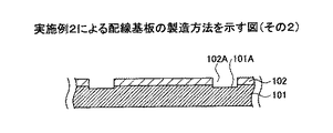
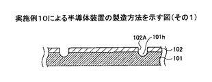
まず、図1Aに示す工程では、例えばCuなどの導電材料よりなる支持基板101上に、例えばスクリーン印刷法により、感光性樹脂材料よりなるソルダーレジスト層102を形成する。この場合、前記ソルダーレジスト層102は、例えばフィルム状のレジスト材料のラミネートや塗布法などにより形成することも可能である。
First, in the step shown in FIG. 1A, a
次に、前記ソルダーレジスト層102に対して、マスクパターン(図示せず)を介して紫外線を照射し、露光させることでパターニングを行い、開口部102Aを形成する。当該開口部102Aからは前記支持基板101が露出した状態となる。
Next, the
次に、図1Bに示す工程において、前記支持基板101を導電経路にした電解メッキにより、前記支持基板101上に、前記開口部102Aに埋設するように、例えばAu/Niよりなる電極103を形成する。なお、Au/Niよりなる電極とは、配線基板が完成した際にAuが表面側(接続面)となるように形成された、Au層とNi層が積層されてなる電極を意味している(以下同じ)。この場合、前記支持基板101が導電材料よりなると電解メッキで前記電極103を形成することが可能であり、前記支持基板101がCuなどの低抵抗の導電材料よりなるとさらに好適である。
Next, in the step shown in FIG. 1B, an
次に、図1Cに示す工程において、前記ソルダーレジスト層102上、および前記電極103上に、例えば、熱硬化性のエポキシ樹脂などよりなる絶縁層(ビルドアップ層)104を形成する。次に、前記絶縁層104に、例えばレーザによりビアホールを形成する。
Next, in the step shown in FIG. 1C, an insulating layer (build-up layer) 104 made of, for example, a thermosetting epoxy resin is formed on the solder resist
次に、当該ビアホールにビアプラグ105を形成するとともに、前記絶縁層104上に、当該ビアプラグ105に接続されるパターン配線106を、例えばセミアディティブ法により形成する。この場合、前記絶縁層104上に無電解メッキでシード層を形成した後、電解メッキにより、前記ビアプラグ105と前記パターン配線106を形成することが好ましい。このようにして、前記ビアプラグ105と前記パターン配線106よりなる配線部が形成される。
Next, a via
次に、図1Dに示す工程において、前記絶縁層104上に、前記パターン配線106を覆うようにソルダーレジスト層107を、例えばスクリーン印刷法により形成する。次に、前記ソルダーレジスト層107に対して、マスクパターン(図示せず)を介して紫外線を照射し、露光させることでパターニングを行い、開口部107Aを形成する。当該開口部107Aからは前記パターン配線106の一部が露出した状態となる。
Next, in a step shown in FIG. 1D, a solder resist
次に、図1Eに示す工程において、前記支持基板101を、例えばウェットエッチングにより除去し、配線基板100を形成する。
Next, in the step shown in FIG. 1E, the
上記の配線基板100は、前記電極103が、例えばマザーボードなどの外部接続機器に接続される側(いわゆるランド側)であり、前記開口部107Aより露出する前記パターン配線106には、例えば半導体チップが接続される。この場合、前記電極103には、例えばソルダーボールなどが形成されていてもよい。また、前記前記開口部107Aより露出する前記パターン配線106には、例えばAu/Niなどよりなる電極や、またはソルダーボール、またはリフロー用のハンダ層などが形成されていてもよい。
In the
本実施例では、前記絶縁層104の形成に先立ち、前記支持基板101上に前記ソルダーレジスト層102を形成していることが特徴の一つである。このため、コアレス構造であって配線基板の両側がソルダーレジスト層で覆われたビルドアップ法による配線基板を形成することが可能となっている。
This embodiment is characterized in that the solder resist
この場合、前記絶縁層104の両側をソルダーレジスト層で保護することが可能となると共に、前記絶縁層104の両側にかかるストレスの差が小さくなり、配線基板の反りが抑制される効果を奏する。
In this case, both sides of the insulating
さらに本実施例の場合、前記ソルダーレジスト層107が前記支持基板101に支持された状態で前記開口部107Aが形成されるため、前記開口部107Aを形成する場合に前記ソルダーレジスト層107の平面度が良好である。そのため、前記開口部107Aの加工精度が良好となり、微細な形状や微細なピッチで前記開口部107Aを形成することが可能となる。
Further, in the case of this embodiment, since the
近年の半導体チップは高集積化・高密度配線化が進んでおり、半導体チップと配線基板の接続部も狭ピッチ化や高密度配線化が進んでいるため、特に前記開口部107Aの位置決め精度や形状の加工精度が必要とされる。本実施例による配線基板の製造方法によれば、これらの要求に対応し、狭ピッチ化・高密度配線化に対応した配線基板を形成することが可能となる。 In recent years, semiconductor chips have been highly integrated and have high density wiring, and the connecting portion between the semiconductor chip and the wiring substrate has also been narrowed in pitch and high density wiring. The processing accuracy of the shape is required. According to the method of manufacturing a wiring board according to the present embodiment, it is possible to form a wiring board corresponding to these demands and corresponding to narrow pitch and high density wiring.
また、本実施例による配線基板の製造方法では、上記の高密度配線に対応しつつ、前記支持基板を除去していわゆるコアレス構造を実現し、配線基板の薄型化を実現している。 Further, in the method for manufacturing the wiring board according to the present embodiment, the so-called coreless structure is realized by removing the support substrate while corresponding to the high-density wiring described above, and the wiring board is thinned.
また、本実施例による配線基板では、前記電極103が、マザーボードなどの外部機器接続側(いわゆるランド側)となっている。そのため、前記開口部102Aの面積(開口径)が、前記開口部107Aの面積(開口径)よりも大きくなっている。例えば、前記半導体チップが接続される前記開口部107Aの開口径は、80μm〜100μm程度、マザーボードなどに接続される前記開口部102Aの開口径は、0.5mm〜1mm程度とその開口径に大きな差が有る。
Further, in the wiring board according to the present embodiment, the
例えば、大きな開口部を形成する場合にレーザを用いた場合、時間を要する問題がある。本実施例では、開口部102Aのパターニングを感光により行っており、レーザの場合に比べて速やかに開口部を形成することが可能となっている。
For example, when a laser is used to form a large opening, there is a problem that takes time. In this embodiment, the patterning of the
また、前記ソルダーレジスト層107を形成する前に、図1Cに示す工程を繰り返し実施することで多層配線構造を有する配線基板を形成することができる。
Further, before the solder resist
例えば、上記のソルダーレジスト層102、107を構成する材料としては、エポキシアクリル系樹脂、エポキシ系樹脂、アクリル系樹脂を用いることができる。また、前記ソルダーレジスト層102、107のパターニング方法としては、上記に示した露光・現像による方法に限定されるものではない。例えば、スクリーン印刷法により、開口部が形成(パターニング)されたソルダーレジスト層を形成するようにしてもよい。この場合、ソルダーレジスト層に感光性のもの以外の材料を用いることが可能である。
For example, as a material constituting the solder resist
また、本実施例では前記電極103と前記ソルダーレジスト層102の厚さが略同じであるが、本発明はこれに限定されるものではなく、必要に応じて以下に示すように様々に前記電極103を変形・変更することが可能である。
In this embodiment, the thickness of the
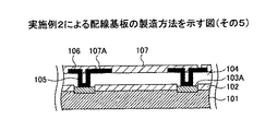
図2A〜図2Fは、本発明の実施例2による配線基板の製造方法を手順を追って示した図である。ただし図中、先に説明した部分には同一の参照符号を付し、説明を省略する。また、特に説明しない部分は実施例1の場合と同様の方法で形成が可能である。 2A to 2F are diagrams illustrating a method of manufacturing a wiring board according to a second embodiment of the present invention, following the procedure. However, in the figure, the same reference numerals are given to the parts described above, and the description will be omitted. Further, portions not particularly described can be formed by the same method as in the first embodiment.
まず、図2Aに示す工程は、図1Aに示した工程と同様であり、前記支持基板101上に前記ソルダーレジスト層102を形成し、当該ソルダーレジスト層102に前記開口部102Aを形成する。
First, the process shown in FIG. 2A is the same as the process shown in FIG. 1A, and the solder resist
次に、図2Bに示す工程において、前記開口部102Aより露出する前記支持基板101をエッチングして凹部101Aを形成する。
Next, in the step shown in FIG. 2B, the
次に、図2Cに示す工程において、実施例1の図1Bに示した工程と同様にして、前記支持基板101を導電経路にした電解メッキにより、前記支持基板101の前記凹部101Aと前記開口部102Aの一部に、埋設するように、例えばAu/Niよりなる電極103Aを形成する。この場合、前記支持基板101が導電材料よりなると電解メッキで前記電極103Aを形成することが可能であり、前記支持基板101がCuなどの低抵抗の導電材料よりなるとさらに好適である。
Next, in the step shown in FIG. 2C, similarly to the step shown in FIG. 1B of Example 1, the
次に、図2D〜図2Fに示す工程において、実施例1の図1C〜図1Eに示した工程と同様にして、前記絶縁層104、前記ビアプラグ105、前記パターン配線106、前記ソルダーレジスト層107、および前記開口部107Aを形成し、前記支持基板101を除去して配線基板100Aを形成する。本実施例の場合、前記電極103Aが前記凹部101Aに形成される以外は、実施例1と同様にして配線基板を形成することが可能であり、実施例1の場合と同様の効果を奏する。
2D to 2F, the insulating
本実施例による配線基板100Aでは、前記電極103Aが、前記ソルダーレジスト層102より突出した構造となっている。このため、例えば前記電極103Aとマザーボードの接続部などをソルダーボールにより接続する場合、当該ソルダーボールと前記電極103Aの接触面積が大きくなるため、電気的な接続信頼性が良好となる効果を奏する。
In the
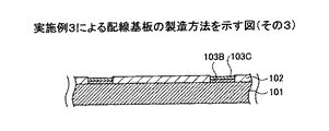
また、図3A〜図3Fは、本発明の実施例3による配線基板の製造方法を手順を追って示した図である。ただし図中、先に説明した部分には同一の参照符号を付し、説明を省略する。また、特に説明しない部分は実施例1の場合と同様の方法で形成が可能である。 FIGS. 3A to 3F are diagrams illustrating the method of manufacturing the wiring board according to the third embodiment of the present invention in order. However, in the figure, the same reference numerals are given to the parts described above, and the description will be omitted. Further, portions not particularly described can be formed by the same method as in the first embodiment.
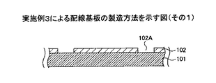
まず、図3Aに示す工程は、図1Aに示した工程と同様であり、前記支持基板101上に前記ソルダーレジスト層102を形成し、当該ソルダーレジスト層102に前記開口部102Aを形成する。
First, the process shown in FIG. 3A is the same as the process shown in FIG. 1A, and the solder resist
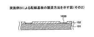
次に、図3Bに示す工程において、前記開口部102Aより露出する前記支持基板101上に、電極高さ調整層103Bを、例えば電解メッキ法により形成する。この場合、前記支持基板101が導電材料よりなると電解メッキで前記電極高さ調整層103Bを形成することが可能であり、前記支持基板101がCuなどの低抵抗の導電材料よりなるとさらに好適である。
Next, in the step shown in FIG. 3B, an electrode
次に、図3Cに示す工程において、実施例1の図1Bに示した工程と同様にして、前記支持基板101および前記電極高さ調整層103Bを導電経路にした電解メッキにより、前記電極高さ調整層103B上に例えばAu/Niよりなる電極103Cを形成する。
Next, in the step shown in FIG. 3C, in the same manner as the step shown in FIG. 1B of Example 1, the electrode height is obtained by electrolytic plating using the
次に、図3D〜図3Fに示す工程において、実施例1の図1C〜図1Eに示した工程と同様にして、前記絶縁層104、前記ビアプラグ105、前記パターン配線106、前記ソルダーレジスト層107、および前記開口部107Aを形成し、前記支持基板101を除去して配線基板100Bを形成する。
Next, in the steps shown in FIGS. 3D to 3F, the insulating
本実施例の場合、図3Fに示す工程においては、前記支持基板101がウェットエッチングにより除去される場合に、前記電極高さ調整層103Bが同様に除去される。このため、前記支持基板101と前記電極高さ調整層103Bは、同じ材料、例えばCuまたはCu合金よりなるようにすることが好ましい。
In the case of this example, in the step shown in FIG. 3F, when the
本実施例の場合、前記電極103Cの形成方法以外は、実施例1と同様にして配線基板を形成することが可能であり、実施例1の場合と同様の効果を奏する。
In the case of this embodiment, it is possible to form a wiring board in the same manner as in Embodiment 1 except for the method of forming the
本実施例による配線基板100Bでは、前記電極103Cが、前記ソルダーレジスト層102の外側の面より凹んだ構造となっている。
In the
このため、前記電極103Cの機械的な強度が良好となる効果を奏する。また、前記電極103Cと、接続端子などが半田付けにより接続される場合、半田が流出して隣接する電極が短絡されることが抑制される効果を奏する。また、前記電極103Cにソルダーボール接合する場合、ソルダーボールの載置を好適に行える効果を奏する。
For this reason, the mechanical strength of the
また、本実施例に示した電極がソルダーレジスト層より凹んだ構造は、次に実施例4に示すような構造に変形することも可能である。 Further, the structure in which the electrode shown in this embodiment is recessed from the solder resist layer can be changed to the structure shown in the next embodiment.
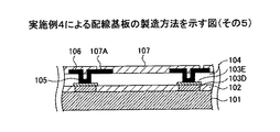
図4A〜図4Fは、本発明の実施例4による配線基板の製造方法を手順を追って示した図である。ただし図中、先に説明した部分には同一の参照符号を付し、説明を省略する。また、特に説明しない部分は実施例3の場合と同様の方法で形成が可能である。 FIGS. 4A to 4F are diagrams illustrating a method of manufacturing a wiring board according to a fourth embodiment of the present invention, following the procedure. However, in the figure, the same reference numerals are given to the parts described above, and the description will be omitted. In addition, portions not particularly described can be formed by the same method as in the third embodiment.
まず、図4Aに示す工程は、図3Aに示した工程と同様であり、前記支持基板101上に前記ソルダーレジスト層102を形成し、当該ソルダーレジスト層102に前記開口部102Aを形成する。
First, the process shown in FIG. 4A is the same as the process shown in FIG. 3A. The solder resist
次に、図4Bに示す工程において、前記開口部102Aより露出する前記支持基板101上に、電極高さ調整層103Dを、例えば電解メッキ法により形成する。実施例3の場合は、例えば前記電極高さ調整層103Bの厚さが前記ソルダーレジスト層102の厚さより薄くなっているが、本実施例の場合には前記電極高さ調整層103Dの厚さが前記ソルダーレジスト層102の厚さと略同じになっている。
Next, in the step shown in FIG. 4B, an electrode
次に、図4Cに示す工程において、実施例3の図3Cに示した工程と同様にして、前記支持基板101と前記電極高さ調整層Dを導電経路にした電解メッキにより、前記電極高さ調整層103D上に例えばAu/Niよりなる電極103Eを形成する。
Next, in the step shown in FIG. 4C, in the same manner as the step shown in FIG. 3C of Example 3, the electrode height is obtained by electrolytic plating using the
次に、図4D〜図4Fに示す工程において、実施例3の図3D〜図3Fに示した工程と同様にして、前記絶縁層104、前記ビアプラグ105、前記パターン配線106、前記ソルダーレジスト層107、および前記開口部107Aを形成し、配線基板100Cを形成する。
Next, in the steps shown in FIGS. 4D to 4F, the insulating
本実施例の場合、実施例3の図3Fに示した工程と同様に、前記支持基板101がウェットエッチングにより除去される場合に、前記電極高さ調整層103Dが同様に除去される。このため、前記支持基板101と前記電極高さ調整層103Dは、同じ材料、例えばCuよりなるようにすることが好ましい。
In the case of this example, similarly to the step shown in FIG. 3F of Example 3, when the
本実施例の場合、前記電極103Eの形成方法以外は、実施例3と同様にして配線基板を形成することが可能であり、実施例3の場合と同様の効果を奏する。
In the case of this example, a wiring board can be formed in the same manner as in Example 3 except for the method of forming the
本実施例による配線基板100Cでは、前記電極103Eが、前記ソルダーレジスト層102の外側の面より凹んだ構造となっており、当該電極103Eは、前記絶縁層104に略埋設した構造となっている。すなわち、前記電極103Eの側壁面全体が、前記絶縁層104に接するように形成されている。このため、実施例3の場合の効果を奏することに加えて、前記電極103Cの機械的な強度が実施例3の場合に比べてさらに良好となる効果を奏する。
In the
また、前記電極103Eの面積は、前記開口部102Aの面積より大きくなっている。これは、電解メッキで前記電極103Eを形成する場合、略等方的に成長するため、電極の横方向への成長があるためである。このため、電極103Eの周縁部がソルダーレジスト層102に被覆された構造となり、電極103Eの強度が良好になる効果を奏する。
The area of the
また、本実施例においては、前記電極高さ調整層の厚さが、前記ソルダーレジスト層102の厚さと略同じ場合を例にとって説明したが、前記電極高さ調整層の厚さは前記ソルダーレジスト層102の厚さ以上であれば、上記に示した場合と同様の効果を奏する。
Further, in this embodiment, the case where the thickness of the electrode height adjustment layer is substantially the same as the thickness of the solder resist
また、例えば上記の実施例1〜実施例4の場合において、前記支持基板101を2枚貼り合わせた構造を用いて、それぞれの支持基板に配線基板を形成することも可能であり、この場合、配線基板を形成する効率を良好とすることができる。
Further, for example, in the case of the above-described Examples 1 to 4, it is also possible to form a wiring board on each supporting board using a structure in which two supporting
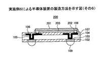
図5は、本発明の実施例5による配線基板の製造方法を示す図である。ただし図中、先に説明した部分には同一の参照符号を付し、説明を省略する。 FIG. 5 is a diagram showing a method of manufacturing a wiring board according to Embodiment 5 of the present invention. However, in the figure, the same reference numerals are given to the parts described above, and the description will be omitted.
図5は、本実施例において、実施例1の図1Dに示した工程に相当する工程を示している。図5を参照するに、本実施例では、前記支持基板101は、支持基板101aと貼り合わせられた構造を有している。当該支持基板101aには、ソルダーレジスト層102a,電極103a,絶縁層104a,ビアプラグ105a,パターン配線106a,ソルダーレジスト層107a、および開口部107bが形成されている。
FIG. 5 shows a process corresponding to the process shown in FIG. Referring to FIG. 5, in this embodiment, the
前記ソルダーレジスト層101a,電極103a,絶縁層104a,ビアプラグ105a,パターン配線106a,ソルダーレジスト層107a、および開口部107bは、それぞれ、前記ソルダーレジスト層101,電極103,絶縁層104,ビアプラグ105,パターン配線106,ソルダーレジスト層107、および開口部107Aに相当し、実施例1の場合と同様にして形成することが可能である。
The solder resist
さらに、本図に示す工程の後、支持基板101と支持基板101aを分離し、実施例1の図1Eに示した工程に相当する工程を実施し、前記支持基板101と前記支持基板101aをウェットエッチングにより除去することで、2つの配線基板を形成することが可能となる。
Further, after the step shown in this figure, the
以上、実施例に説明した構造・材料などは一例であり、適宜変形・変更が可能であることは明らかである。例えば、前記電極103,103A,103C,103E,103aなどを構成する材料は、Au/Niに限定されず、例えば、Au/Ni/Cu,Au/Pd/Ni,Au/Pd/Ni/Cu,Au/Pd/Ni/Pd,Au/Pd/Ni/Pd/Cu,Sn−Pb/Ni,Sn−Pb/Ni/Cu,Sn−Ag/Ni,Sn−Ag/Ni/Cu、などを用いることが可能である。なお、上記の材料は、配線基板が完成した際に、表面(外側)となる金属層から順に記載している。
As described above, the structures, materials, and the like described in the embodiments are merely examples, and it is obvious that modifications and changes can be appropriately made. For example, the material constituting the
また、必要に応じて、例えば配線基板の周縁部に補強板を設けるなどして配線基板の剛性を高める構造としてもよい。 Further, if necessary, for example, a reinforcing plate may be provided on the periphery of the wiring board to increase the rigidity of the wiring board.
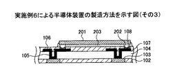
次に、上記の配線基板に対して、半導体チップを実装して半導体装置を製造する例を、図6A〜6Bを用いて手順を追って説明する。ただし図中、先に説明した部分には同一の参照符号を付し、説明を省略する。なお、以下の例では、実施例1に記載した実装基板に半導体チップを実装する場合を例にとって、説明するが、実施例2〜実施例5に記載した実装基板にも同様の手順で半導体チップを実装して半導体装置を製造することができる。 Next, an example of manufacturing a semiconductor device by mounting a semiconductor chip on the above wiring board will be described step by step with reference to FIGS. However, in the figure, the same reference numerals are given to the parts described above, and the description will be omitted. In the following example, a case where a semiconductor chip is mounted on the mounting board described in the first embodiment will be described as an example. However, the semiconductor chip is also mounted on the mounting board described in the second to fifth embodiments in the same procedure. Can be mounted to manufacture a semiconductor device.
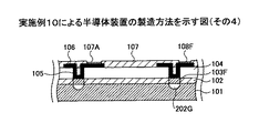
本実施例による半導体装置の製造方法では、まず、実施例1に示した、図1A〜図1Dに示した工程を実施する。 In the method of manufacturing a semiconductor device according to this example, first, the steps shown in FIGS. 1A to 1D shown in Example 1 are performed.
次に、図6Aに示す工程で、前記ソルダーレジスト層107の前記開口部107Aから露出した前記パターン配線106上に、Au/Niよりなる電極108を、例えばスパッタリング法、電解メッキ法、または無電解メッキ法などにより形成する。
Next, in the step shown in FIG. 6A, an
次に、図6Bに示す工程において、半導体チップ接続端子(例えば半田ボール)202が形成された半導体チップ201を、前記半導体チップ接続端子202と前記電極108が電気的に接続されるようにして、フリップチップ実装する。前記半導体チップ201は、前記電極108を介して前記パターン配線106に電気的に接続される。
Next, in the step shown in FIG. 6B, the
次に、前記半導体チップ201と前記ソルダーレジスト層107の間に、アンダーフィル203を浸透させて硬化させることで、実装部分の絶縁と信頼性を確保する。
Next, the
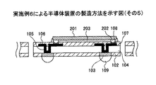
次に、図6Cに示す工程において、図1Eに示した工程と同様にして、前記支持基板101を、例えばウェットエッチングにより除去する。
Next, in the step shown in FIG. 6C, the
次に、図6Dに示す工程において、前記支持基板101を除去したことで露出した前記電極103に、外部接続端子(例えば半田ボール)109を形成する。なお、本実施例の場合には、BGA(Ball Grid Array)構造を有する半導体装置を製造する場合を例にとって説明しているため、前記電極103には半田ボールを形成するが、これに限定されるものではない。
Next, in the step shown in FIG. 6D, external connection terminals (for example, solder balls) 109 are formed on the
例えば、PGA(Pin Grid Array)構造を有する半導体装置では、前記電極103には外部接続端子としてピンが形成される。また、外部接続端子の形成を省略し、配線基板(半導体装置)の電極自体を外部接続端子として用いるLGA(Land Grid Array)構造としてもよい。
For example, in a semiconductor device having a PGA (Pin Grid Array) structure, a pin is formed on the
次に、図6Eに示す工程において、前記基板104、ソルダーレジスト層102、107を切断し、個片化することで、図6Fに示す半導体装置200を形成することができる。この場合、前記基板104上に、複数の半導体チップ201が実装された構造を形成し、その後基板104(ソルダーレジスト層102、107)を切断して個片化することで、複数の半導体装置を形成することができる。なお、本実施例では半導体装置を1個のみ図示している。
Next, in the step shown in FIG. 6E, the
本実施例による半導体装置の製造方法によれば、実施例1に記載した効果と同様の効果を奏し、薄型化が可能であって、高密度配線に対応可能な半導体装置を製造することができる。 According to the method for manufacturing a semiconductor device according to the present embodiment, it is possible to manufacture a semiconductor device that exhibits the same effects as those described in the first embodiment, can be reduced in thickness, and can handle high-density wiring. .
また、半導体チップの実装方法は、実施例6に記載した場合に限定されるものではない。図7は、実施例7による半導体装置の製造方法を示す図である。ただし図中、先に説明した部分には同一の参照符号を付し、説明を省略する。 Further, the semiconductor chip mounting method is not limited to the case described in the sixth embodiment. FIG. 7 is a diagram illustrating the method of manufacturing the semiconductor device according to the seventh embodiment. However, in the figure, the same reference numerals are given to the parts described above, and the description will be omitted.
本実施例による半導体装置の製造方法では、まず、実施例6の図6Aまでの工程を実施する。 In the method of manufacturing a semiconductor device according to the present embodiment, first, the steps up to FIG.
次に、図7に示す工程(実施例6の図6Bの工程に対応)において、半導体チップ201Aを前記ソルダーレジスト層107上に搭載し、さらに前記半導体チップ201Aと前記電極108を、ワイヤ202Aで接続する。この場合、前記半導体チップ201Aと前記ソルダーレジスト層107の間には樹脂製のフィルムを挿入し接着するようにしてもよい。さらに、前記半導体チップ201Aを、樹脂層203Aで封止する。
Next, in the process shown in FIG. 7 (corresponding to the process of FIG. 6B in Example 6), the
図7の工程の後は、実施例6に示した図6C〜図6Fに相当する工程を実施すれば実施例6の場合と同様にして半導体装置を製造することができる。このように、半導体チップの実装は、ワイヤボンディングによって行うことも可能である(以下の例においても同様)。 After the step of FIG. 7, the semiconductor device can be manufactured in the same manner as in Example 6 by performing the steps corresponding to FIGS. 6C to 6F shown in Example 6. In this manner, the semiconductor chip can be mounted by wire bonding (the same applies to the following examples).
また、上記の実施例6または実施例7において、外部接続端子(半田ボール)109の形成方法を変更してもよい。 Further, in the above-described Example 6 or Example 7, the method of forming the external connection terminal (solder ball) 109 may be changed.
図8A〜図8Bは、実施例8による半導体装置の製造方法を示す図である。ただし図中、先に説明した部分には同一の参照符号を付し、説明を省略する。 8A to 8B are diagrams illustrating a method for manufacturing a semiconductor device according to the eighth embodiment. However, in the figure, the same reference numerals are given to the parts described above, and the description will be omitted.
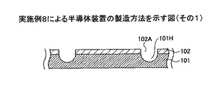
本実施例による半導体装置の製造方法では、まず、実施例1の図1Aに示した工程を実施する。 In the method of manufacturing a semiconductor device according to this embodiment, first, the process shown in FIG. 1A of Embodiment 1 is performed.
次に、図8Aに示す工程において、前記開口部102Aより露出する前記支持基板101を、例えば前記ソルダーレジスト層102をマスクにしてエッチングし、凹部101Hを形成する。
Next, in the step shown in FIG. 8A, the
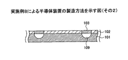
次に、図8Bに示す工程において、前記支持基板101を導電経路にしたはんだ等の電解メッキにより、前記凹部101Hを埋設するように、外部接続端子109を形成する。さらに、当該外部接続端子109上に、電解メッキにより、図1Bに示した工程と同様にして、例えばAu/Niよりなる電極103を形成する。
Next, in the step shown in FIG. 8B,
以下の工程は、実施例7または実施例8と同様の工程を実施すればよい。すなわち、図1C〜図1Dに示した工程と、図6A〜図6Fに示した工程を実施すればよい。また、図6Bの工程は図7の工程に置き換えてもよい。この場合、図6Dに示した外部接続端子を形成する工程は不要となる。このようにして、外部接続端子を形成する方法・工程を変更してもよい。 The following steps may be performed in the same manner as in Example 7 or Example 8. That is, the steps shown in FIGS. 1C to 1D and the steps shown in FIGS. 6A to 6F may be performed. Further, the process of FIG. 6B may be replaced with the process of FIG. In this case, the step of forming the external connection terminal shown in FIG. 6D is not necessary. In this way, the method / process for forming the external connection terminal may be changed.
また、上記の実施例6〜実施例8では、半導体チップをソルダーレジスト層107の側に実装したが、本発明による半導体装置の製造方法は、これに限定されるものではない。例えば、以下に説明するように、半導体チップを、支持基板を除去したことで露出する電極に接続されるように実装してもよい。
Further, in the above Examples 6 to 8, the semiconductor chip is mounted on the solder resist
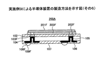
図9A〜図9Fは、実施例9による半導体装置の製造方法を示す図である。ただし図中、先に説明した部分には同一の参照符号を付し、説明を省略する。 9A to 9F are views showing a method for manufacturing a semiconductor device according to the ninth embodiment. However, in the figure, the same reference numerals are given to the parts described above, and the description will be omitted.
本実施例による半導体装置の製造方法では、まず、実施例1に示した、図1A〜図1Dに示した工程に相当する工程を実施する。 In the method of manufacturing a semiconductor device according to the present embodiment, first, steps corresponding to the steps shown in FIGS. 1A to 1D shown in the first embodiment are performed.
次に、図9Aに示す工程で、前記ソルダーレジスト層107の前記開口部107Aから露出した前記パターン配線106上に、Au/Niよりなる電極108Fを、例えばスパッタリング法、電解メッキ法または無電解メッキ法などにより形成する。
Next, in the step shown in FIG. 9A, an
なお、本実施例の場合、電極103F(実施例6〜8の場合の電極103に相当)に半導体チップが実装されるため、実施例6〜8の電極103に比べて電極103Fの面積が小さくなっている。また、前記電極108F(実施例6〜8の場合の電極108に相当)に後の工程において外部接続端子(例えば半田ボールなど)が形成されるため、実施例6〜8の電極108に比べて電極108Fの面積が大きくなっている。ここまでの工程においては、これらの電極の形状(電極に応じたソルダーレジストの開口部)以外は、実施例6〜8の場合と同様にする。
In this embodiment, since the semiconductor chip is mounted on the
次に、図9Bに示す工程において、図1Eに示した工程と同様にして、前記支持基板101を、例えばウェットエッチングにより除去する。ここで、前記電極103Fが露出する。
Next, in the step shown in FIG. 9B, the
次に、図9Cに示す工程において、半導体チップ接続端子(例えば半田ボール)202Fが形成された半導体チップ201Fを、前記半導体チップ接続端子202Fと前記電極103Fが電気的に接続されるようにして、フリップチップ実装する。前記半導体チップ201Fは、前記電極103Fを介して前記パターン配線106に電気的に接続される。すなわち本実施例の場合には、前記支持基板101を除去したことで露出する前記電極103Fの側に半導体チップを実装している。
Next, in the step shown in FIG. 9C, the
次に、前記半導体チップ201Fと前記ソルダーレジスト層102の間に、アンダーフィル203Fを浸透させて硬化させることで、実装部分の絶縁と信頼性を確保する。
Next, the
次に、図9Dに示す工程において、前記電極108Fに、外部接続端子(半田ボール)109Fを形成する。なお、実施例6の場合と同様に、前記外部接続端子109Fの形成を省略するか、または前記電極108Fに外部接続端子としてピンを形成してもよい。
Next, in the step shown in FIG. 9D, external connection terminals (solder balls) 109F are formed on the
次に、図9Eに示し工程において、前記基板104、ソルダーレジスト層102、107を切断し、個片化することで、図9Fに示す半導体装置200Aを形成することができる。
Next, in the step shown in FIG. 9E, the
本実施例による半導体装置の製造方法によれば、実施例6に記載した効果と同様の効果を奏し、薄型化が可能であって、高密度配線に対応可能な半導体装置を製造することができる。また、半導体チップの実装は、実施例7に示したようにワイヤボンディングと樹脂封止により行ってもよい。 According to the method for manufacturing a semiconductor device according to the present embodiment, it is possible to manufacture a semiconductor device that exhibits the same effects as those described in Embodiment 6, can be reduced in thickness, and can handle high-density wiring. . Further, the semiconductor chip may be mounted by wire bonding and resin sealing as shown in the seventh embodiment.
また、上記の実施例9において、半導体チップを実装するための半導体チップ接続端子(例えば半田ボール)を、以下に説明するように基板側に設けるようにしてもよい。 Further, in the ninth embodiment, semiconductor chip connection terminals (for example, solder balls) for mounting a semiconductor chip may be provided on the substrate side as described below.
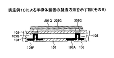
図10A〜図10Fは、実施例10による半導体装置の製造方法を示す図である。ただし図中、先に説明した部分には同一の参照符号を付し、説明を省略する。 10A to 10F are diagrams illustrating the method for manufacturing the semiconductor device according to the tenth embodiment. However, in the figure, the same reference numerals are given to the parts described above, and the description will be omitted.
本実施例による半導体装置の製造方法では、まず、実施例1の図1Aに示した工程に相当する工程を実施する。但し、実施例9で説明したように、ソルダーレジスト層102の開口部102Aは、半導体チップの実装に対応して、実施例1の場合よりも小さくする。
In the method of manufacturing a semiconductor device according to this embodiment, first, a process corresponding to the process shown in FIG. However, as described in the ninth embodiment, the
次に、図10Aに示す工程において、前記開口部102Aより露出する前記支持基板101を、例えば前記ソルダーレジスト層102をマスクにしてエッチングし、凹部101hを形成する。
Next, in the step shown in FIG. 10A, the
次に、図10Bに示す工程において、前記支持基板101を導電経路にしたはんだ等の電解メッキにより、前記凹部101hを埋設するように、半導体チップ接続端子(例えば半田ボール)202Gを形成する。さらに、当該半導体チップ接続端子202G上に、電解メッキにより、例えばAu/Niよりなる電極103Fを形成する。
Next, in the step shown in FIG. 10B, a semiconductor chip connection terminal (eg, solder ball) 202G is formed so as to bury the
次に、図10Cに示す工程では、実施例1の図1Cに示した工程と同様にして、絶縁層104、ビアプラグ105、およびパターン配線106を形成する。
Next, in the step shown in FIG. 10C, the insulating
次に、図10Dに示す工程において、実施例1の図1Dの工程と同様にしてパターン配線106の一部が露出する開口部107Aを有するソルダーレジスト層107を形成する。
Next, in the process shown in FIG. 10D, a solder resist
次に、実施例9の図9Aの工程と同様にして、前記ソルダーレジスト層107の前記開口部107Aから露出した前記パターン配線106上に、Au/Niよりなる電極108Fを形成する。
Next, an
次に、図10Eに示す工程において、前記支持基板101を、例えばウェットエッチングにより除去する。ここで、前記半田ボール202Gが露出することになる。
Next, in the step shown in FIG. 10E, the
次に、図10Fに示す工程において、半導体チップ201Gを、露出した前記半導体チップ接続端子202G上に実装する。この場合、半導体チップ接続端子が基板側に形成されているため、半導体チップ接続端子を半導体チップ側に形成しておく必要がなくなる。
Next, in the step shown in FIG. 10F, the semiconductor chip 201G is mounted on the exposed semiconductor
さらに、前記半導体チップ201Gと前記ソルダーレジスト層102の間に、アンダーフィル203Gを浸透させて硬化させることで、実装部分の絶縁と信頼性を確保する。
Further, the
図10F以降の工程は、実施例9の図9Eの工程に相当する工程を実施することで、半導体装置を形成することができる。 The processes after FIG. 10F can form a semiconductor device by performing a process corresponding to the process of FIG.
このように、半導体チップと基板を接続するための半導体チップ接続端子(例えば半田ボール)を、基板側に形成しておくことも可能である。 In this way, semiconductor chip connection terminals (for example, solder balls) for connecting the semiconductor chip and the substrate can be formed on the substrate side.
また、実施例6〜実施例10に示した半導体装置の製造方法では、配線部が1層である場合を例にとって説明したが、本発明はこれに限定されるものではない。例えば、ビアプラグ105とパターン配線106よりなる配線部が、多層に積層されて形成された、多層配線構造を有する半導体装置(配線基板)の製造の場合に対しても、本発明を適用可能であることは明らかである。
In the method for manufacturing a semiconductor device shown in the sixth to tenth embodiments, the case where the wiring portion has one layer has been described as an example. However, the present invention is not limited to this. For example, the present invention can also be applied to the case of manufacturing a semiconductor device (wiring board) having a multilayer wiring structure in which wiring portions including via
以上、本発明を好ましい実施例について説明したが、本発明は上記の特定の実施例に限定されるものではなく、特許請求の範囲に記載した要旨内において様々な変形・変更が可能である。 Although the present invention has been described with reference to the preferred embodiments, the present invention is not limited to the specific embodiments described above, and various modifications and changes can be made within the scope described in the claims.
本発明によれば、薄型化が可能であって、高密度配線に対応可能な配線基板の製造方法、および当該配線基板に半導体装置が実装されてなる半導体装置の製造方法を提供することができる。 According to the present invention, it is possible to provide a method of manufacturing a wiring board that can be thinned and can handle high-density wiring, and a method of manufacturing a semiconductor device in which a semiconductor device is mounted on the wiring board. .
100,100A,100B,100C 配線基板
101,101a 支持基板
102,107,107a ソルダーレジスト層
103,103a,103A,103C,103E 電極
104,104a 絶縁層
105,105a ビアプラグ
106,106a パターン配線
102A,107A 開口部
201,201F,201G 半導体チップ
202F,202G 半田ボール
203F,203G アンダーフィル
100, 100A, 100B,
Claims (13)
前記第1の開口部に電極を形成する第2の工程と、
前記電極上に絶縁層を形成し、当該絶縁層に前記電極に接続される配線部を形成する第3の工程と、
当該配線部上に第2の開口部を有する第2のソルダーレジスト層を形成する第4の工程と、
前記支持基板を除去する第5の工程と、を有することを特徴とする配線基板の製造方法。 A first step of forming a first solder resist layer having a first opening on a support substrate;
A second step of forming an electrode in the first opening;
A third step of forming an insulating layer on the electrode and forming a wiring portion connected to the electrode on the insulating layer;
A fourth step of forming a second solder resist layer having a second opening on the wiring portion;
And a fifth step of removing the support substrate.
前記別の支持基板に第3の開口部を有する第3のソルダーレジスト層を形成する第6の工程と、
前記第3の開口部に別の電極を形成する第7の工程と、
前記別の電極を覆うように別の絶縁層を形成し、当該別の絶縁層に、前記別の電極に接続される別の配線部を形成する第8の工程と、
前記別の配線部を覆うように第4の開口部を有する第4のソルダーレジスト層を形成する第9の工程と、
前記別の支持基板を除去する第10の工程と、をさらに有することを特徴とする請求項1乃至8のうち、いずれか1項記載の配線基板の製造方法。 The support substrate is bonded to another support substrate,
A sixth step of forming a third solder resist layer having a third opening on the other support substrate;
A seventh step of forming another electrode in the third opening;
An eighth step of forming another insulating layer so as to cover the another electrode, and forming another wiring portion connected to the other electrode in the other insulating layer;
A ninth step of forming a fourth solder resist layer having a fourth opening so as to cover the another wiring portion;
The method according to claim 1, further comprising: a tenth step of removing the another support substrate.
前記第4の工程の後に、前記第2の開口部から前記配線部に電気的に接続されるように半導体チップを実装する実装工程をさらに有することを特徴とする半導体装置の製造方法。 A method for manufacturing a semiconductor device using the method for manufacturing a wiring board according to claim 1, wherein:
A method of manufacturing a semiconductor device, further comprising a mounting step of mounting a semiconductor chip so as to be electrically connected from the second opening to the wiring portion after the fourth step.
前記第5の工程の後に、前記電極を介して前記配線部に電気的に接続されるように半導体チップを実装する実装工程をさらに有することを特徴とする半導体装置の製造方法。 A method for manufacturing a semiconductor device using the method for manufacturing a wiring board according to claim 1, wherein:
A method of manufacturing a semiconductor device, further comprising a mounting step of mounting a semiconductor chip so as to be electrically connected to the wiring portion via the electrode after the fifth step.
Priority Applications (8)
| Application Number | Priority Date | Filing Date | Title |
|---|---|---|---|
| JP2006014199A JP4146864B2 (en) | 2005-05-31 | 2006-01-23 | WIRING BOARD AND MANUFACTURING METHOD THEREOF, SEMICONDUCTOR DEVICE AND SEMICONDUCTOR DEVICE MANUFACTURING METHOD |
| US11/419,887 US8015700B2 (en) | 2005-05-31 | 2006-05-23 | Method of fabricating wiring board and method of fabricating semiconductor device |
| KR1020060046012A KR20060124576A (en) | 2005-05-31 | 2006-05-23 | Method of fabricating wiring board and method of fabricating semiconductor device |
| TW095118980A TWI437668B (en) | 2005-05-31 | 2006-05-29 | Wiring board, semiconductor device, method of fabricating wiring board and method of fabricating semiconductor device |
| CN2006100836413A CN1873935B (en) | 2005-05-31 | 2006-05-31 | Method of fabricating wiring board and method of fabricating semiconductor device |
| US13/196,129 US8455770B2 (en) | 2005-05-31 | 2011-08-02 | Method of fabricating wiring board and method of fabricating semiconductor device |
| KR1020120088942A KR101344800B1 (en) | 2005-05-31 | 2012-08-14 | Wiring board and semiconductor device |
| US13/873,504 US9155195B2 (en) | 2005-05-31 | 2013-04-30 | Wiring board and semiconductor device |
Applications Claiming Priority (2)
| Application Number | Priority Date | Filing Date | Title |
|---|---|---|---|
| JP2005159993 | 2005-05-31 | ||
| JP2006014199A JP4146864B2 (en) | 2005-05-31 | 2006-01-23 | WIRING BOARD AND MANUFACTURING METHOD THEREOF, SEMICONDUCTOR DEVICE AND SEMICONDUCTOR DEVICE MANUFACTURING METHOD |
Related Child Applications (1)
| Application Number | Title | Priority Date | Filing Date |
|---|---|---|---|
| JP2008133992A Division JP4980295B2 (en) | 2005-05-31 | 2008-05-22 | Wiring substrate manufacturing method and semiconductor device manufacturing method |
Publications (3)
| Publication Number | Publication Date |
|---|---|
| JP2007013092A true JP2007013092A (en) | 2007-01-18 |
| JP2007013092A5 JP2007013092A5 (en) | 2008-01-17 |
| JP4146864B2 JP4146864B2 (en) | 2008-09-10 |
Family
ID=37464013
Family Applications (1)
| Application Number | Title | Priority Date | Filing Date |
|---|---|---|---|
| JP2006014199A Active JP4146864B2 (en) | 2005-05-31 | 2006-01-23 | WIRING BOARD AND MANUFACTURING METHOD THEREOF, SEMICONDUCTOR DEVICE AND SEMICONDUCTOR DEVICE MANUFACTURING METHOD |
Country Status (4)
| Country | Link |
|---|---|
| US (3) | US8015700B2 (en) |
| JP (1) | JP4146864B2 (en) |
| KR (2) | KR20060124576A (en) |
| TW (1) | TWI437668B (en) |
Cited By (13)
| Publication number | Priority date | Publication date | Assignee | Title |
|---|---|---|---|---|
| JP2008270346A (en) * | 2007-04-17 | 2008-11-06 | Shinko Electric Ind Co Ltd | Method for manufacturing wiring circuit board, method for manufacturing semiconductor device, and wiring circuit board |
| KR20100133317A (en) | 2009-06-11 | 2010-12-21 | 신코 덴키 코교 가부시키가이샤 | Method of manufacturing wiring substrate |
| JP2012069972A (en) * | 2011-11-04 | 2012-04-05 | Shinko Electric Ind Co Ltd | Manufacturing method of wiring board and manufacturing method of semiconductor package |
| JP2012124363A (en) * | 2010-12-09 | 2012-06-28 | Ngk Spark Plug Co Ltd | Manufacturing method for multilayer wiring board |
| JP2013009006A (en) * | 2012-09-26 | 2013-01-10 | Shinko Electric Ind Co Ltd | Wiring substrate and manufacturing method of the same |
| US8476754B2 (en) | 2009-06-03 | 2013-07-02 | Shinko Electric Industries Co., Ltd. | Wiring substrate and method of manufacturing the same |
| US8502398B2 (en) | 2007-10-05 | 2013-08-06 | Shinko Electric Industries Co., Ltd. | Wiring board, semiconductor apparatus and method of manufacturing them |
| US8610287B2 (en) | 2009-12-21 | 2013-12-17 | Shinko Electric Industries Co., Ltd. | Wiring substrate and method of manufacturing the same |
| JP2015073068A (en) * | 2013-10-01 | 2015-04-16 | 旭徳科技股▲ふん▼有限公司 | Package carrier |
| US9258899B2 (en) | 2007-05-30 | 2016-02-09 | Shinko Electric Industries Co., Ltd. | Method of fabricating a wiring board |
| JP2017163058A (en) * | 2016-03-10 | 2017-09-14 | パナソニックIpマネジメント株式会社 | LED module |
| JP2017163053A (en) * | 2016-03-10 | 2017-09-14 | パナソニックIpマネジメント株式会社 | LED module |
| JP7382175B2 (en) | 2019-08-26 | 2023-11-16 | ローム株式会社 | semiconductor equipment |
Families Citing this family (15)
| Publication number | Priority date | Publication date | Assignee | Title |
|---|---|---|---|---|
| JP5557439B2 (en) * | 2008-10-24 | 2014-07-23 | ピーエスフォー ルクスコ エスエイアールエル | Semiconductor device and manufacturing method thereof |
| US8569894B2 (en) | 2010-01-13 | 2013-10-29 | Advanced Semiconductor Engineering, Inc. | Semiconductor package with single sided substrate design and manufacturing methods thereof |
| JP5623308B2 (en) * | 2010-02-26 | 2014-11-12 | 日本特殊陶業株式会社 | Multilayer wiring board and manufacturing method thereof |
| TWI411075B (en) | 2010-03-22 | 2013-10-01 | Advanced Semiconductor Eng | Semiconductor package and manufacturing method thereof |
| JP5638269B2 (en) | 2010-03-26 | 2014-12-10 | 日本特殊陶業株式会社 | Multilayer wiring board |
| JP5566771B2 (en) | 2010-05-18 | 2014-08-06 | 日本特殊陶業株式会社 | Multilayer wiring board |
| JP5502624B2 (en) * | 2010-07-08 | 2014-05-28 | 新光電気工業株式会社 | Wiring board manufacturing method and wiring board |
| US9406658B2 (en) | 2010-12-17 | 2016-08-02 | Advanced Semiconductor Engineering, Inc. | Embedded component device and manufacturing methods thereof |
| JP5795225B2 (en) * | 2011-09-27 | 2015-10-14 | 新光電気工業株式会社 | Wiring board manufacturing method |
| US8698008B2 (en) | 2011-12-12 | 2014-04-15 | Advance Materials Corporation | Packaging substrate and fabrication method thereof |
| KR20150064445A (en) * | 2013-12-03 | 2015-06-11 | 삼성전기주식회사 | Coreless Board for Semi-conductor Package and the Method of Manufacturing the same, the Method of Manufacturing of Semi-Conductor Package Using the same |
| JP2015231003A (en) * | 2014-06-06 | 2015-12-21 | イビデン株式会社 | Circuit board and manufacturing method of the same |
| CN105407651B (en) * | 2014-09-12 | 2018-06-26 | 深南电路有限公司 | A kind of method that solder mask is set on circuit board |
| KR102231100B1 (en) * | 2014-10-02 | 2021-03-23 | 삼성전기주식회사 | Printed circuit board and method for manufacturing thereof |
| KR20230096382A (en) * | 2021-12-23 | 2023-06-30 | 삼성전기주식회사 | Method for manufacturing printed circuit board |
Family Cites Families (32)
| Publication number | Priority date | Publication date | Assignee | Title |
|---|---|---|---|---|
| US4889584A (en) * | 1989-03-31 | 1989-12-26 | Meiko Electronics Co., Ltd. | Method of producing conductor circuit boards |
| JPH04322252A (en) | 1991-04-23 | 1992-11-12 | Hitachi Ltd | Preparation of photosetting resist composition |
| US5886877A (en) * | 1995-10-13 | 1999-03-23 | Meiko Electronics Co., Ltd. | Circuit board, manufacturing method therefor, and bump-type contact head and semiconductor component packaging module using the circuit board |
| CN1265691C (en) * | 1996-12-19 | 2006-07-19 | 揖斐电株式会社 | Printed wiring board and method for manufacturing the same |
| JPH11307883A (en) | 1998-04-20 | 1999-11-05 | Ngk Spark Plug Co Ltd | Wiring board |
| JP3437453B2 (en) | 1998-07-06 | 2003-08-18 | イビデン株式会社 | Printed wiring board for mounting IC chip and method of manufacturing the same |
| US6915566B2 (en) * | 1999-03-01 | 2005-07-12 | Texas Instruments Incorporated | Method of fabricating flexible circuits for integrated circuit interconnections |
| JP3949849B2 (en) * | 1999-07-19 | 2007-07-25 | 日東電工株式会社 | Manufacturing method of interposer for chip size package and interposer for chip size package |
| US6210992B1 (en) * | 1999-08-31 | 2001-04-03 | Micron Technology, Inc. | Controlling packaging encapsulant leakage |
| JP2001094259A (en) | 1999-09-24 | 2001-04-06 | Jsr Corp | Multilayer wiring board and manufacturing method |
| EP1259103B1 (en) * | 2000-02-25 | 2007-05-30 | Ibiden Co., Ltd. | Multilayer printed wiring board and method for producing multilayer printed wiring board |
| JP3677429B2 (en) * | 2000-03-09 | 2005-08-03 | Necエレクトロニクス株式会社 | Method of manufacturing flip chip type semiconductor device |
| JP3546961B2 (en) | 2000-10-18 | 2004-07-28 | 日本電気株式会社 | Wiring board for mounting semiconductor device, method of manufacturing the same, and semiconductor package |
| JP2002261190A (en) | 2001-02-28 | 2002-09-13 | Sony Corp | Semiconductor device, method for manufacturing the same and electronic equipment |
| MY131114A (en) * | 2001-06-27 | 2007-07-31 | Shinko Electric Ind Co | Wiring substrate having position information |
| JP3910387B2 (en) * | 2001-08-24 | 2007-04-25 | 新光電気工業株式会社 | Semiconductor package, manufacturing method thereof, and semiconductor device |
| CN1224305C (en) * | 2001-10-31 | 2005-10-19 | 新光电气工业株式会社 | Method for mfg. mulfilayer circuit board for semiconductor device |
| JP3666591B2 (en) * | 2002-02-01 | 2005-06-29 | 株式会社トッパンNecサーキットソリューションズ | Manufacturing method of semiconductor chip mounting substrate |
| US7474538B2 (en) * | 2002-05-27 | 2009-01-06 | Nec Corporation | Semiconductor device mounting board, method of manufacturing the same, method of inspecting the same, and semiconductor package |
| JP2004066017A (en) * | 2002-08-01 | 2004-03-04 | Nippon Paint Co Ltd | Method of forming of solder resist film |
| JP3990962B2 (en) * | 2002-09-17 | 2007-10-17 | 新光電気工業株式会社 | Wiring board manufacturing method |
| KR100499006B1 (en) * | 2002-12-30 | 2005-07-01 | 삼성전기주식회사 | Manufacturing method for package substrate without electrolytic plating lead |
| JP4067507B2 (en) | 2003-03-31 | 2008-03-26 | 三洋電機株式会社 | Semiconductor module and manufacturing method thereof |
| TWI305018B (en) | 2003-03-31 | 2009-01-01 | Sanyo Electric Co | Semiconductor module and method for making same |
| WO2004103039A1 (en) * | 2003-05-19 | 2004-11-25 | Dai Nippon Printing Co., Ltd. | Double-sided wiring board, double-sided wiring board manufacturing method, and multilayer wiring board |
| JP2005129904A (en) | 2003-09-29 | 2005-05-19 | Sanyo Electric Co Ltd | Semiconductor device and method of manufacturing the same |
| JP4271590B2 (en) * | 2004-01-20 | 2009-06-03 | 新光電気工業株式会社 | Semiconductor device and manufacturing method thereof |
| US7468645B2 (en) * | 2004-01-29 | 2008-12-23 | Sanyo Electric Co., Ltd. | Signal line circuit device |
| TWI255535B (en) * | 2004-03-31 | 2006-05-21 | Sanyo Electric Co | Device mounting board and semiconductor apparatus using the same |
| JP4361826B2 (en) * | 2004-04-20 | 2009-11-11 | 新光電気工業株式会社 | Semiconductor device |
| JP4333492B2 (en) | 2004-06-16 | 2009-09-16 | ソニー株式会社 | Method for manufacturing circuit module body |
| US7361979B2 (en) * | 2004-12-29 | 2008-04-22 | Tessera, Inc. | Multi-sheet conductive substrates for microelectronic devices and methods for forming such substrates |
-
2006
- 2006-01-23 JP JP2006014199A patent/JP4146864B2/en active Active
- 2006-05-23 US US11/419,887 patent/US8015700B2/en active Active
- 2006-05-23 KR KR1020060046012A patent/KR20060124576A/en not_active Application Discontinuation
- 2006-05-29 TW TW095118980A patent/TWI437668B/en active
-
2011
- 2011-08-02 US US13/196,129 patent/US8455770B2/en active Active
-
2012
- 2012-08-14 KR KR1020120088942A patent/KR101344800B1/en active IP Right Grant
-
2013
- 2013-04-30 US US13/873,504 patent/US9155195B2/en active Active
Cited By (20)
| Publication number | Priority date | Publication date | Assignee | Title |
|---|---|---|---|---|
| US8225502B2 (en) | 2007-04-17 | 2012-07-24 | Shinko Electric Industries Co., Ltd. | Wiring board manufacturing method |
| JP2008270346A (en) * | 2007-04-17 | 2008-11-06 | Shinko Electric Ind Co Ltd | Method for manufacturing wiring circuit board, method for manufacturing semiconductor device, and wiring circuit board |
| US9258899B2 (en) | 2007-05-30 | 2016-02-09 | Shinko Electric Industries Co., Ltd. | Method of fabricating a wiring board |
| US8502398B2 (en) | 2007-10-05 | 2013-08-06 | Shinko Electric Industries Co., Ltd. | Wiring board, semiconductor apparatus and method of manufacturing them |
| TWI447874B (en) * | 2007-10-05 | 2014-08-01 | Shinko Electric Ind Co | Wiring board, semiconductor apparatus and method of manufacturing them |
| US8779602B2 (en) | 2007-10-05 | 2014-07-15 | Shinko Electric Industries Co., Ltd. | Wiring board, semiconductor apparatus and method of manufacturing them |
| US8749046B2 (en) | 2009-06-03 | 2014-06-10 | Shinko Electric Industries Co., Ltd. | Wiring substrate and method of manufacturing the same |
| US8476754B2 (en) | 2009-06-03 | 2013-07-02 | Shinko Electric Industries Co., Ltd. | Wiring substrate and method of manufacturing the same |
| KR20100133317A (en) | 2009-06-11 | 2010-12-21 | 신코 덴키 코교 가부시키가이샤 | Method of manufacturing wiring substrate |
| US8790504B2 (en) | 2009-06-11 | 2014-07-29 | Shinko Electric Industries Co., Ltd. | Method of manufacturing wiring substrate |
| US8610287B2 (en) | 2009-12-21 | 2013-12-17 | Shinko Electric Industries Co., Ltd. | Wiring substrate and method of manufacturing the same |
| US8535546B2 (en) | 2010-12-09 | 2013-09-17 | Ngk Spark Plug Co., Ltd. | Method of manufacturing multilayer wiring substrate |
| JP2012124363A (en) * | 2010-12-09 | 2012-06-28 | Ngk Spark Plug Co Ltd | Manufacturing method for multilayer wiring board |
| JP2012069972A (en) * | 2011-11-04 | 2012-04-05 | Shinko Electric Ind Co Ltd | Manufacturing method of wiring board and manufacturing method of semiconductor package |
| JP2013009006A (en) * | 2012-09-26 | 2013-01-10 | Shinko Electric Ind Co Ltd | Wiring substrate and manufacturing method of the same |
| JP2015073068A (en) * | 2013-10-01 | 2015-04-16 | 旭徳科技股▲ふん▼有限公司 | Package carrier |
| US9433099B2 (en) | 2013-10-01 | 2016-08-30 | Subtron Technology Co., Ltd. | Package carrier |
| JP2017163058A (en) * | 2016-03-10 | 2017-09-14 | パナソニックIpマネジメント株式会社 | LED module |
| JP2017163053A (en) * | 2016-03-10 | 2017-09-14 | パナソニックIpマネジメント株式会社 | LED module |
| JP7382175B2 (en) | 2019-08-26 | 2023-11-16 | ローム株式会社 | semiconductor equipment |
Also Published As
| Publication number | Publication date |
|---|---|
| US20110286189A1 (en) | 2011-11-24 |
| US8455770B2 (en) | 2013-06-04 |
| TWI437668B (en) | 2014-05-11 |
| US8015700B2 (en) | 2011-09-13 |
| KR20060124576A (en) | 2006-12-05 |
| TW200703590A (en) | 2007-01-16 |
| KR20120109427A (en) | 2012-10-08 |
| KR101344800B1 (en) | 2013-12-26 |
| US20130235543A1 (en) | 2013-09-12 |
| US20060270211A1 (en) | 2006-11-30 |
| JP4146864B2 (en) | 2008-09-10 |
| US9155195B2 (en) | 2015-10-06 |
Similar Documents
| Publication | Publication Date | Title |
|---|---|---|
| JP4146864B2 (en) | WIRING BOARD AND MANUFACTURING METHOD THEREOF, SEMICONDUCTOR DEVICE AND SEMICONDUCTOR DEVICE MANUFACTURING METHOD | |
| JP4980295B2 (en) | Wiring substrate manufacturing method and semiconductor device manufacturing method | |
| US10383228B2 (en) | Electronic component device and method for manufacturing the same | |
| JP5101451B2 (en) | Wiring board and manufacturing method thereof | |
| US8227711B2 (en) | Coreless packaging substrate and method for fabricating the same | |
| TWI557855B (en) | Package carrier and manufacturing method thereof | |
| JP2008300507A (en) | Wiring substrate and manufacturing process of the same | |
| JP2008060573A (en) | Manufacturing method of electronic element built-in printed circuit board | |
| JP2004193549A (en) | Package substrate plated without plated lead-in wire and its manufacturing method | |
| US9711476B2 (en) | Wiring board and electronic component device | |
| JP2018032657A (en) | Printed wiring board and method for manufacturing printed wiring board | |
| JP2008016817A (en) | Buried pattern substrate and its manufacturing method | |
| TW201424497A (en) | Circuit board and method for manufacturing same | |
| JP2007088477A (en) | Method for manufacturing substrate provided with cavity | |
| JP2005243850A (en) | Multilayer printed wiring board and its manufacturing method | |
| JP2010080528A (en) | Method of manufacturing semiconductor package | |
| KR101039774B1 (en) | Method of fabricating a metal bump for printed circuit board | |
| JP2009147080A (en) | Semiconductor device package and method of manufacturing the same | |
| TWI496243B (en) | Method for fabricating embedded component semiconductor package | |
| JP4591098B2 (en) | Manufacturing method of semiconductor device mounting substrate | |
| JP5511922B2 (en) | Wiring board and manufacturing method thereof | |
| TWI461134B (en) | Supporting substrate and fabrication thereof | |
| JP2005093930A (en) | Multilayer substrate and method of manufacturing the same | |
| JP2013084812A (en) | Method of manufacturing semiconductor package, and semiconductor package |
Legal Events
| Date | Code | Title | Description |
|---|---|---|---|
| A521 | Request for written amendment filed |
Free format text: JAPANESE INTERMEDIATE CODE: A523 Effective date: 20071127 |
|
| A621 | Written request for application examination |
Free format text: JAPANESE INTERMEDIATE CODE: A621 Effective date: 20071127 |
|
| A871 | Explanation of circumstances concerning accelerated examination |
Free format text: JAPANESE INTERMEDIATE CODE: A871 Effective date: 20071127 |
|
| A131 | Notification of reasons for refusal |
Free format text: JAPANESE INTERMEDIATE CODE: A131 Effective date: 20080108 |
|
| A975 | Report on accelerated examination |
Free format text: JAPANESE INTERMEDIATE CODE: A971005 Effective date: 20080325 |
|
| A131 | Notification of reasons for refusal |
Free format text: JAPANESE INTERMEDIATE CODE: A131 Effective date: 20080401 |
|
| A521 | Request for written amendment filed |
Free format text: JAPANESE INTERMEDIATE CODE: A523 Effective date: 20080522 |
|
| TRDD | Decision of grant or rejection written | ||
| A01 | Written decision to grant a patent or to grant a registration (utility model) |
Free format text: JAPANESE INTERMEDIATE CODE: A01 Effective date: 20080617 |
|
| A01 | Written decision to grant a patent or to grant a registration (utility model) |
Free format text: JAPANESE INTERMEDIATE CODE: A01 |
|
| A61 | First payment of annual fees (during grant procedure) |
Free format text: JAPANESE INTERMEDIATE CODE: A61 Effective date: 20080620 |
|
| R150 | Certificate of patent or registration of utility model |
Free format text: JAPANESE INTERMEDIATE CODE: R150 Ref document number: 4146864 Country of ref document: JP Free format text: JAPANESE INTERMEDIATE CODE: R150 |
|
| FPAY | Renewal fee payment (event date is renewal date of database) |
Free format text: PAYMENT UNTIL: 20110627 Year of fee payment: 3 |
|
| FPAY | Renewal fee payment (event date is renewal date of database) |
Free format text: PAYMENT UNTIL: 20110627 Year of fee payment: 3 |
|
| FPAY | Renewal fee payment (event date is renewal date of database) |
Free format text: PAYMENT UNTIL: 20120627 Year of fee payment: 4 |
|
| FPAY | Renewal fee payment (event date is renewal date of database) |
Free format text: PAYMENT UNTIL: 20120627 Year of fee payment: 4 |
|
| FPAY | Renewal fee payment (event date is renewal date of database) |
Free format text: PAYMENT UNTIL: 20130627 Year of fee payment: 5 |