JP2006520006A - Optical device, method of forming an optical device, and optical assembly incorporating an optical device - Google Patents
Optical device, method of forming an optical device, and optical assembly incorporating an optical device Download PDFInfo
- Publication number
- JP2006520006A JP2006520006A JP2005507041A JP2005507041A JP2006520006A JP 2006520006 A JP2006520006 A JP 2006520006A JP 2005507041 A JP2005507041 A JP 2005507041A JP 2005507041 A JP2005507041 A JP 2005507041A JP 2006520006 A JP2006520006 A JP 2006520006A
- Authority
- JP
- Japan
- Prior art keywords
- optical
- waveguide
- end wall
- substrate
- component
- Prior art date
- Legal status (The legal status is an assumption and is not a legal conclusion. Google has not performed a legal analysis and makes no representation as to the accuracy of the status listed.)
- Granted
Links
Images


Classifications
-
- G—PHYSICS
- G02—OPTICS
- G02B—OPTICAL ELEMENTS, SYSTEMS OR APPARATUS
- G02B6/00—Light guides; Structural details of arrangements comprising light guides and other optical elements, e.g. couplings
- G02B6/24—Coupling light guides
- G02B6/42—Coupling light guides with opto-electronic elements
- G02B6/4201—Packages, e.g. shape, construction, internal or external details
- G02B6/4219—Mechanical fixtures for holding or positioning the elements relative to each other in the couplings; Alignment methods for the elements, e.g. measuring or observing methods especially used therefor
- G02B6/4228—Passive alignment, i.e. without a detection of the degree of coupling or the position of the elements
-
- G—PHYSICS
- G02—OPTICS
- G02B—OPTICAL ELEMENTS, SYSTEMS OR APPARATUS
- G02B6/00—Light guides; Structural details of arrangements comprising light guides and other optical elements, e.g. couplings
- G02B6/24—Coupling light guides
- G02B6/26—Optical coupling means
- G02B6/264—Optical coupling means with optical elements between opposed fibre ends which perform a function other than beam splitting
- G02B6/266—Optical coupling means with optical elements between opposed fibre ends which perform a function other than beam splitting the optical element being an attenuator
-
- G—PHYSICS
- G02—OPTICS
- G02B—OPTICAL ELEMENTS, SYSTEMS OR APPARATUS
- G02B6/00—Light guides; Structural details of arrangements comprising light guides and other optical elements, e.g. couplings
- G02B6/10—Light guides; Structural details of arrangements comprising light guides and other optical elements, e.g. couplings of the optical waveguide type
- G02B6/12—Light guides; Structural details of arrangements comprising light guides and other optical elements, e.g. couplings of the optical waveguide type of the integrated circuit kind
- G02B6/12007—Light guides; Structural details of arrangements comprising light guides and other optical elements, e.g. couplings of the optical waveguide type of the integrated circuit kind forming wavelength selective elements, e.g. multiplexer, demultiplexer
-
- G—PHYSICS
- G02—OPTICS
- G02B—OPTICAL ELEMENTS, SYSTEMS OR APPARATUS
- G02B6/00—Light guides; Structural details of arrangements comprising light guides and other optical elements, e.g. couplings
- G02B6/24—Coupling light guides
- G02B6/26—Optical coupling means
- G02B6/28—Optical coupling means having data bus means, i.e. plural waveguides interconnected and providing an inherently bidirectional system by mixing and splitting signals
- G02B6/293—Optical coupling means having data bus means, i.e. plural waveguides interconnected and providing an inherently bidirectional system by mixing and splitting signals with wavelength selective means
- G02B6/29346—Optical coupling means having data bus means, i.e. plural waveguides interconnected and providing an inherently bidirectional system by mixing and splitting signals with wavelength selective means operating by wave or beam interference
- G02B6/2935—Mach-Zehnder configuration, i.e. comprising separate splitting and combining means
- G02B6/29352—Mach-Zehnder configuration, i.e. comprising separate splitting and combining means in a light guide
-
- G—PHYSICS
- G02—OPTICS
- G02B—OPTICAL ELEMENTS, SYSTEMS OR APPARATUS
- G02B6/00—Light guides; Structural details of arrangements comprising light guides and other optical elements, e.g. couplings
- G02B6/24—Coupling light guides
- G02B6/26—Optical coupling means
- G02B6/30—Optical coupling means for use between fibre and thin-film device
-
- G—PHYSICS
- G02—OPTICS
- G02B—OPTICAL ELEMENTS, SYSTEMS OR APPARATUS
- G02B6/00—Light guides; Structural details of arrangements comprising light guides and other optical elements, e.g. couplings
- G02B6/24—Coupling light guides
- G02B6/42—Coupling light guides with opto-electronic elements
- G02B6/4201—Packages, e.g. shape, construction, internal or external details
- G02B6/4204—Packages, e.g. shape, construction, internal or external details the coupling comprising intermediate optical elements, e.g. lenses, holograms
-
- G—PHYSICS
- G02—OPTICS
- G02B—OPTICAL ELEMENTS, SYSTEMS OR APPARATUS
- G02B6/00—Light guides; Structural details of arrangements comprising light guides and other optical elements, e.g. couplings
- G02B6/10—Light guides; Structural details of arrangements comprising light guides and other optical elements, e.g. couplings of the optical waveguide type
- G02B6/12—Light guides; Structural details of arrangements comprising light guides and other optical elements, e.g. couplings of the optical waveguide type of the integrated circuit kind
- G02B2006/12133—Functions
- G02B2006/12147—Coupler
-
- G—PHYSICS
- G02—OPTICS
- G02B—OPTICAL ELEMENTS, SYSTEMS OR APPARATUS
- G02B6/00—Light guides; Structural details of arrangements comprising light guides and other optical elements, e.g. couplings
- G02B6/10—Light guides; Structural details of arrangements comprising light guides and other optical elements, e.g. couplings of the optical waveguide type
- G02B6/12—Light guides; Structural details of arrangements comprising light guides and other optical elements, e.g. couplings of the optical waveguide type of the integrated circuit kind
- G02B2006/12133—Functions
- G02B2006/12164—Multiplexing; Demultiplexing
-
- G—PHYSICS
- G02—OPTICS
- G02B—OPTICAL ELEMENTS, SYSTEMS OR APPARATUS
- G02B6/00—Light guides; Structural details of arrangements comprising light guides and other optical elements, e.g. couplings
- G02B6/10—Light guides; Structural details of arrangements comprising light guides and other optical elements, e.g. couplings of the optical waveguide type
- G02B6/12—Light guides; Structural details of arrangements comprising light guides and other optical elements, e.g. couplings of the optical waveguide type of the integrated circuit kind
- G02B2006/12166—Manufacturing methods
-
- G—PHYSICS
- G02—OPTICS
- G02B—OPTICAL ELEMENTS, SYSTEMS OR APPARATUS
- G02B6/00—Light guides; Structural details of arrangements comprising light guides and other optical elements, e.g. couplings
- G02B6/24—Coupling light guides
- G02B6/26—Optical coupling means
- G02B6/28—Optical coupling means having data bus means, i.e. plural waveguides interconnected and providing an inherently bidirectional system by mixing and splitting signals
- G02B6/2804—Optical coupling means having data bus means, i.e. plural waveguides interconnected and providing an inherently bidirectional system by mixing and splitting signals forming multipart couplers without wavelength selective elements, e.g. "T" couplers, star couplers
-
- G—PHYSICS
- G02—OPTICS
- G02B—OPTICAL ELEMENTS, SYSTEMS OR APPARATUS
- G02B6/00—Light guides; Structural details of arrangements comprising light guides and other optical elements, e.g. couplings
- G02B6/24—Coupling light guides
- G02B6/36—Mechanical coupling means
- G02B6/3628—Mechanical coupling means for mounting fibres to supporting carriers
- G02B6/3632—Mechanical coupling means for mounting fibres to supporting carriers characterised by the cross-sectional shape of the mechanical coupling means
- G02B6/3636—Mechanical coupling means for mounting fibres to supporting carriers characterised by the cross-sectional shape of the mechanical coupling means the mechanical coupling means being grooves
-
- G—PHYSICS
- G02—OPTICS
- G02B—OPTICAL ELEMENTS, SYSTEMS OR APPARATUS
- G02B6/00—Light guides; Structural details of arrangements comprising light guides and other optical elements, e.g. couplings
- G02B6/24—Coupling light guides
- G02B6/36—Mechanical coupling means
- G02B6/3628—Mechanical coupling means for mounting fibres to supporting carriers
- G02B6/3648—Supporting carriers of a microbench type, i.e. with micromachined additional mechanical structures
- G02B6/3652—Supporting carriers of a microbench type, i.e. with micromachined additional mechanical structures the additional structures being prepositioning mounting areas, allowing only movement in one dimension, e.g. grooves, trenches or vias in the microbench surface, i.e. self aligning supporting carriers
-
- G—PHYSICS
- G02—OPTICS
- G02B—OPTICAL ELEMENTS, SYSTEMS OR APPARATUS
- G02B6/00—Light guides; Structural details of arrangements comprising light guides and other optical elements, e.g. couplings
- G02B6/24—Coupling light guides
- G02B6/42—Coupling light guides with opto-electronic elements
- G02B6/4201—Packages, e.g. shape, construction, internal or external details
- G02B6/4219—Mechanical fixtures for holding or positioning the elements relative to each other in the couplings; Alignment methods for the elements, e.g. measuring or observing methods especially used therefor
- G02B6/422—Active alignment, i.e. moving the elements in response to the detected degree of coupling or position of the elements
- G02B6/4221—Active alignment, i.e. moving the elements in response to the detected degree of coupling or position of the elements involving a visual detection of the position of the elements, e.g. by using a microscope or a camera
- G02B6/4224—Active alignment, i.e. moving the elements in response to the detected degree of coupling or position of the elements involving a visual detection of the position of the elements, e.g. by using a microscope or a camera using visual alignment markings, e.g. index methods
Landscapes
- Physics & Mathematics (AREA)
- General Physics & Mathematics (AREA)
- Optics & Photonics (AREA)
- Engineering & Computer Science (AREA)
- Microelectronics & Electronic Packaging (AREA)
- Chemical & Material Sciences (AREA)
- Crystallography & Structural Chemistry (AREA)
- Optical Couplings Of Light Guides (AREA)
- Optical Integrated Circuits (AREA)
Abstract
光学構成要素は、水平部材101から突出する2つの側壁108とほぼ透明な1つの端壁100とを有する水平部材101を備える。端壁、各側壁および水平部材は内側体積の部分106を部分的に取り囲むと共に、上記端壁の少なくとも一部分に対して任意の適切な様式で光学機能性が付与される。光学アセンブリは、光学構成要素の端壁からの反射または光学構成要素端壁を通る透過のいずれかにより端部結合がなされた平面導波路250および第2導波路210、230と共に導波路基板200上に取り付けられた光学構成要素を備える。取り付けられた光学構成要素の内側体積の部分には、平面導波路の端部が受容され得る。各々の導波路に対する光学構成要素の適切な位置決めは、光学構成要素および/または導波路基板上の整列表面および/または整列マーク124、224により促進され得る。The optical component comprises a horizontal member 101 having two side walls 108 projecting from the horizontal member 101 and one end wall 100 that is substantially transparent. The end walls, each side wall, and the horizontal member partially surround the inner volume portion 106 and are provided with optical functionality in any suitable manner for at least a portion of the end wall. The optical assembly is on the waveguide substrate 200 with the planar waveguide 250 and the second waveguides 210, 230 end coupled either by reflection from the end wall of the optical component or transmission through the end wall of the optical component. An optical component attached to the. A portion of the inner volume of the attached optical component can receive the end of the planar waveguide. Proper positioning of the optical components relative to each waveguide may be facilitated by alignment surfaces and / or alignment marks 124, 224 on the optical components and / or waveguide substrate.
Description
本発明は、光学構成要素に関する。特に、本願明細書中においては、導波路間の自由空間光伝搬のための反射的および/または透過的な光学構成要素が開示されている。 The present invention relates to optical components. In particular, reflective and / or transmissive optical components for free space light propagation between waveguides are disclosed herein.
関連出願
本願は、ヘンリー・エー・ブラウベルト(Henry A. Blauvelt)およびジョエル・エス・パスラスキ(Joel S. Paslaski)の名義にて2002年11月12日に先行出願された「導波路間における自由空間光伝搬のための反射的および/または透過的な光学構成要素(Reflective and/or transmissive optical component for free-space optical propagation between waveguides)」という名称の同時係属の米国仮出願第60/425,370号の優先権を主張するが、この仮出願の内容は、本願明細書中で完全に記述されることにより本願明細書中に組み込まれている。さらに、本発明は、デビッド・ダブリュ・ヴェノイ(David W. Vernooy)、ジョエル・エス・パスラスキ(Joel S. Paslaski)およびグイド・ハンツィクラ(Guido Hunziker)の名義にて2003年4月29日に先行出願された「低プロフィル形コアおよび薄寸コアの導波路、ならびにその作製方法および使用方法(Low-profile-core and thin-core optical waveguides and methods of fabrication and use thereof)」という名称の同時係属の米国仮出願第60/466,799号の優先権を主張するが、この仮出願の内容は、本願明細書中で完全に記述されることにより本願明細書中に組み込まれている。
RELATED APPLICATION This application is filed in the name of Henry A. Blauvelt and Joel S. Paslaski on November 12, 2002, entitled “Freedom Between Waveguides”. Of co-pending US Provisional Application No. 60 / 425,370 entitled “Reflective and / or transmissive optical components for free-space optical propagation between waveguides”. Although claimed in priority, the contents of this provisional application are incorporated herein by reference in their entirety. In addition, the present invention is filed earlier on April 29, 2003 in the name of David W. Vernooy, Joel S. Paslaski and Guido Hunziker. Co-pending US named “Low-profile-core and thin-core optical waveguides and methods of fabrication and use reagents” This application claims the priority of provisional application 60 / 466,799, the contents of which are hereby incorporated by reference in their entirety.
通信および他の分野にて使用される種々の光学デバイスを実現するためには、平面的光導波路(planar optical waveguide)が適している。平面導波路(planar waveguide)(すなわち、平面的光導波路)に加え、平面導波路基板は多くの場合に(基板上への作製および/または載置により)、上記基板上に光学構成要素/光学デバイスを載置するための整列用構造/支持構造(すなわち、支持/整列用構造)と、上記基板上に光ファイバおよび/または光ファイバのテーパ物を位置決めするためのV溝および/または他の整列用構造/支持構造と、補償板、回折格子、フィルタおよび/または他の光学要素(光学構成要素)/光学デバイスと、上記基板上で有効な光学デバイスに対する電子的アクセスを可能にする電気接点および/または電気配線(traces)と、他の適切な構成要素とを有する。
従来は、平面的光導波路に対して複数の光学構成要素/光学デバイスを適切に位置決めして使用するための具体的な構造に関しては記述されていない。本願明細書中においては、後述のように、限定的なものとしてではなく、ミラー、ビームスプリッタ、ビーム結合器、フィルタ、レンズ等の反射的および/または透過的な複数の光学要素(光学構成要素)が、1個以上の平面的光導波路と共に使用されるために開示されており、かつ、上記複数の光学要素間における自由空間光伝搬および/または端部連結のために開示されている。
In order to realize various optical devices used in communication and other fields, a planar optical waveguide is suitable. In addition to planar waveguides (ie, planar optical waveguides), planar waveguide substrates are often optical components / optical on the substrate (by fabrication and / or placement on the substrate). An alignment structure / support structure for mounting the device (ie, a support / alignment structure), and a V-groove and / or other for positioning an optical fiber and / or optical fiber taper on the substrate; Alignment structures / support structures, compensators, diffraction gratings, filters and / or other optical elements (optical components) / optical devices and electrical contacts that allow electronic access to optical devices available on the substrate And / or electrical traces and other suitable components.
Heretofore, no specific structure has been described for properly positioning and using a plurality of optical components / optical devices with respect to a planar optical waveguide. In the present specification, as described later, a plurality of reflective and / or transparent optical elements (optical components) such as a mirror, a beam splitter, a beam combiner, a filter, and a lens are not intended to be limiting. ) For use with one or more planar optical waveguides and for free space light propagation and / or end coupling between the plurality of optical elements.
本発明は、平面的光導波路に対して複数の光学構成要素/光学デバイスを適切に位置決めして使用することが可能な光学構成要素であって、平面的光導波路間の自由空間光伝搬のための反射的および/または透過的な光学構成要素を提供することを目的とするものである。 The present invention is an optical component capable of appropriately positioning and using a plurality of optical components / optical devices with respect to a planar optical waveguide, and for free-space light propagation between the planar optical waveguides. It is intended to provide a reflective and / or transmissive optical component.
光学構成要素は、水平部材から突出する2つの側壁とほぼ透明な1つの端壁とを有する水平部材を備え得る。上記端壁、各々の上記側壁および水平部材は、内側体積の部分を部分的に取り囲み得ると共に、上記端壁の少なくとも一部分に対しては光学機能性が付与される。光学機能性を付与する例としては(限定的なものとしてではなく)、i)上記光学構成要素層の少なくとも一方の表面上に少なくとも一層の光学被覆を形成する段階、ii)光学構成要素層に対して少なくとも1つの湾曲表面を形成する段階、iii)上記端壁の少なくとも一方の表面に対し、空間的に変化する表面プロフィルを形成する段階、iv)上記光学構成要素層に対し、空間的に変化する少なくとも1種類の光学特性を提供する段階、v)光学構成要素層に対し、少なくとも1種類の異方的な光学特性を提供する段階、および/または、vi)光学構成要素層に対し、スペクトル的に変化する少なくとも1種類の光学特性を提供する段階が挙げられる。 The optical component may comprise a horizontal member having two side walls projecting from the horizontal member and one substantially transparent end wall. The end walls, each of the side walls and the horizontal member may partially surround a portion of the inner volume and provide optical functionality to at least a portion of the end walls. Examples of (but not limited to) providing optical functionality include: i) the step of forming at least one optical coating on at least one surface of the optical component layer, ii) the optical component layer Forming at least one curved surface on the surface; iii) forming a spatially varying surface profile on at least one surface of the end wall; and iv) spatially on the optical component layer. Providing at least one optical property that varies, v) providing at least one anisotropic optical property for the optical component layer, and / or vi) for the optical component layer, Providing at least one optical property that varies spectrally.
1つの方法として、上記光学構成要素は基板上に形成され得ると共に、上記基板の一部分は上記水平部材を形成し、かつ、各々の上記側壁および端壁は上記基板から突出する。代替的な方法として、光学装置が基板上に形成され得ると共に、上記端壁は、上記基板上に形成された光学構成要素層を有し、その後に、上記基板の下方から基板材料が除去される。各々の上記側壁および水平部材は、上記光学構成要素層と共に上記基板の残部から分離された基板材料から形成される。これらの方法のいずれかが、多数の光学構成要素を同時に作製するためにウェハ規模(wafer scale)にて実現され得る。光学機能性は、棒状体(bar)レベルにて、および/または、個々の構成要素レベルにて、ウェハ規模で付与され得る。 As one method, the optical component can be formed on a substrate, a portion of the substrate forms the horizontal member, and each of the sidewalls and end walls protrudes from the substrate. As an alternative, an optical device can be formed on the substrate and the end wall has an optical component layer formed on the substrate, after which the substrate material is removed from below the substrate. The Each of the sidewalls and horizontal members is formed from a substrate material that is separated from the remainder of the substrate along with the optical component layer. Any of these methods can be implemented on a wafer scale to produce multiple optical components simultaneously. Optical functionality can be imparted on a wafer scale at the bar level and / or at the individual component level.
光学アセンブリは、導波路基板上に取り付けられた前述の光学構成要素と、上記基板上に形成された平面導波路(平面的光導波路)と、上記基板上に配置された第2導波路とを備え得る。各々の上記導波路は、上記光学構成要素の端壁からの反射、または、上記光学構成要素の端壁を通る透過のいずれかにより光学的に端部結合がなされる。上記光学構成要素は、平面導波路の端部を上記内側体積の部分に受容させて上記導波路基板上に取り付けられ得る。各々の上記導波路に対する上記光学構成要素の適切な位置決めは、上記光学構成要素および/または導波路基板上の整列表面および/または整列マークにより促進され得る。 The optical assembly includes the above-described optical component mounted on a waveguide substrate, a planar waveguide (planar optical waveguide) formed on the substrate, and a second waveguide disposed on the substrate. Can be prepared. Each of the waveguides is optically end coupled by either reflection from the end wall of the optical component or transmission through the end wall of the optical component. The optical component may be mounted on the waveguide substrate with the end of the planar waveguide received in the portion of the inner volume. Proper positioning of the optical component relative to each of the waveguides may be facilitated by alignment surfaces and / or alignment marks on the optical component and / or waveguide substrate.
本願明細書中に開示された光学構成要素および/または光学アセンブリの目的および利点は、図面中に示されかつ以下の明細書中の記述説明および/または特許請求の範囲の各請求項に示されて開示された好適実施例を参照すれば明らかとなり得る。 The objects and advantages of the optical components and / or optical assemblies disclosed herein are set forth in the drawings and are set forth in the following description and / or claims. It will be apparent with reference to the preferred embodiments disclosed above.
各図に示された種々の構造の相対寸法比は、本発明をさらに明確に示すために変更され得ることを銘記されたい。また一方で、種々の光学デバイス、光導波路、光ファイバ、光学構成要素、光学モード、整列用部材/支持部材、溝等の相対寸法は、相互に対して、かつ、夫々の横方向および/または長手方向の寸法比において変更され得る。多くの図において、光学要素の横次元(transverse dimension)は明瞭化のために長手次元(longitudinal dimension)に対して拡大されることから、長手方向の位置に対する横次元の変化は誇張して示される。 It should be noted that the relative dimensional ratios of the various structures shown in each figure can be varied to more clearly illustrate the present invention. On the other hand, the relative dimensions of the various optical devices, optical waveguides, optical fibers, optical components, optical modes, alignment / support members, grooves, etc. are relative to each other and in the respective lateral direction and / or It can be varied in the longitudinal dimension ratio. In many figures, the transverse dimension of an optical element is exaggerated with respect to its longitudinal position, since the transverse dimension of the optical element is enlarged with respect to the longitudinal dimension for clarity. .
各図に示された実施例は例示的であり、本願明細書中に開示され、かつ/または、権利請求がなされた本発明の範囲を制限するものと解釈されるべきでない。 The embodiments shown in the figures are exemplary and should not be construed to limit the scope of the invention as disclosed and / or claimed herein.
実施例の詳細な説明
本願明細書中に記述される光導波路(光ファイバおよび平面導波路を含む)の多くは、唯1個のもしくは数個の最低次の光学モードをサポートすべき寸法および設計パラメータを有する。可視および近赤外(IR)の波長にて、結果的な光学モードは、横方向の広がりにおいて典型的には数μmから約10μmまたは数μmから約15μmである。導波路の性質に依存し、導かれた光学モードは略々円筒状に対称的とされ得るか、または、ほぼ直交する夫々の横次元に沿う横方向の広がりにおいて相当に異なり得る。これらの導波路のモードおよびサイズは、典型的にはサポートを行う導波路の端面を越えて実質的に回折的挙動を呈することから、サポートを行う導波路の端面から十分に遠く実質的に収束的/発散的となる(多くの場合にNAは約0.1より大きい)。それゆえに、端部結合がなされた導波路同士の間で動作上容認可能なレベルより高い度合いの光パワー伝達を達成するには、以下の適合化の1つ以上が必要とされ得る。すなわち、このような適合化として、導波路端面同士の間において案内されない光学経路長を、特定の光学アセンブリに対して実施可能な限り小さく維持すること、一方もしくは両方の導波路の端部を適合化させ、当該導波路の端面における光学モードの回折的挙動を緩和させること、および、モードの空間的特性を再度焦点合わせし、再作像しまたは別様に操作して導波路同士の間における端部結合を増進するために、導波路同士間に1個以上の付加的な光学要素を挿入することが挙げられる。
Detailed Description of the Embodiments Many of the optical waveguides (including optical fibers and planar waveguides) described herein are sized and designed to support only one or several lowest order optical modes. Has parameters. At visible and near infrared (IR) wavelengths, the resulting optical mode is typically a few μm to about 10 μm or a few μm to about 15 μm in the lateral extent. Depending on the nature of the waveguide, the guided optical modes can be made substantially cylindrically symmetric, or can vary considerably in the lateral extent along their respective transverse dimensions that are approximately orthogonal. The mode and size of these waveguides typically exhibit a substantially diffractive behavior beyond the end face of the supporting waveguide, so that they are substantially converged far enough from the end face of the supporting waveguide. (In many cases NA is greater than about 0.1). Therefore, one or more of the following adaptations may be required to achieve a higher degree of optical power transfer between the end-coupled waveguides than is operably acceptable. That is, such adaptations include keeping the optical path length that is not guided between the waveguide end faces as small as practicable for a particular optical assembly, or adapting the end of one or both waveguides. To relax the diffractive behavior of the optical modes at the end faces of the waveguide, and refocus, re-image, or otherwise manipulate the spatial characteristics of the modes between the waveguides In order to enhance end coupling, one or more additional optical elements may be inserted between the waveguides.
導波路に基づく光学システムまたは導波路に基づく多重構成要素式の光学デバイスにおいては多くの場合に、導波路内においては容易に実現され得ない光学機能性が提供されるべきであることから、当該光学機能性は、各々の導波路の端面間の光学経路内に介設された(反射的および/または透過的な)光学構成要素により提供されるべきであり、導波路同士の間における(反射的光学構成要素から反射され、かつ/または、透過的光学構成要素を透過した)光伝搬は案内されない(すなわち自由空間とされる)というのが実情である。このようにして、光学システムを通した全体的な透過率を作用的に容認可能なレベルにまたはそれより高いレベルに維持しながら光学機能性を実現する上で典型的には、光学システムもしくは多重構成要素式の光学デバイスを先行段落部分に記述された如く適合化することが必要である。 In many cases, waveguide-based optical systems or waveguide-based multi-component optical devices should provide optical functionality that cannot be easily implemented in a waveguide. The optical functionality should be provided by optical components (reflective and / or transparent) interposed in the optical path between the end faces of each waveguide, and between the waveguides (reflective The reality is that light propagation reflected from and / or transmitted through a transmissive optical component is not guided (ie free space). In this way, the optical system or multiplexing is typically used to achieve optical functionality while maintaining the overall transmission through the optical system at an operationally acceptable level or higher. It is necessary to adapt the component optical device as described in the preceding paragraph.
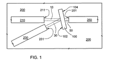
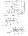
図1は、光導波路210、230および250と共に平面導波路基板200上に配置された光学構成要素100を含む光学アセンブリの概略図であり、上記光導波路の内の少なくとも1つは基板200上に形成された平面導波路である。光パワーは、導波路210、230および250によりサポートされる夫々の伝搬モードの内の1つ以上のモードにおいて、当該導波路の各々を伝搬し得る。各々の導波路210、230および250は、夫々の端面211、231および251にて終端するが、当該端面を通して光パワーは、光パワーの端部伝達(等価的に、端部伝達、端部結合、端部結合による光パワー伝達、光パワーの端部結合伝達、端部結合伝達)により夫々の導波路に進入し、かつ/または、夫々の導波路を出射することが可能であり、光ビーム10、30および50は自由に伝搬する(「自由に伝搬する」とは、導波路により提供される如き横方向案内がないことを表す)。導波路210および230ならびに光学構成要素100は、当該光学構成要素100の表面102および/または104からの光ビーム10の反射(表面104からの反射に対する光学構成要素100を通した復光路透過と、図1、図2、図3A、図3B、図4Aおよび図4Bに示された表面102からのみの反射とを含む)により、導波路210および230の間における光パワーの反射結合式端部伝達を可能とすべく適切に配置され得る。同様にして、導波路210および250ならびに光学構成要素100は、当該光学構成要素100およびその表面102および104を通る光ビーム10および/または50の透過により導波路210と250との間で光パワーの透過結合式端部伝達を可能とすべく適切に配置され得る。
FIG. 1 is a schematic diagram of an optical assembly that includes an
光学構成要素100は、当該光学構成要素から反射され、かつ/または、当該光学構成要素を透過した光ビームの強度、空間的特性、偏光特性および/またはスペクトル特性を改変すべく(すなわち当該光学構成要素に関して光学機能性を付与すべく)、多数の様式で適合化され得る。それゆえに、図1の包括的な光学アセンブリは、本願明細書の開示内容および/または添付の特許請求の範囲の各請求項の範囲内に留まりながら(導波路同士間の端部結合を増進する役割も果たす)光学構成要素100を介して多様な光学機能性を実現すべく採用され得る。限定的なものとしてではなく、光学機能性の付与の例としては、i)上記光学構成要素上の少なくとも一方の表面上に少なくとも一層の光学被覆を形成する段階、ii)上記光学構成要素に対して少なくとも1つの湾曲表面を形成する段階、iii)上記光学構成要素の少なくとも一方の表面に対して、空間的に変化する表面プロフィルを形成する段階、iv)上記光学構成要素に対して、空間的に変化する少なくとも1種類の光学特性を付与する段階、v)上記光学構成要素に対して、少なくとも1種類の異方的な光学特性を付与する段階、および/または、vi)上記光学構成要素に対して、スペクトル的に変化する少なくとも1種類の光学特性を付与する段階が挙げられる。(限定的なものとしてではなく)光学機能性を付与する光学構成要素100の適合化のさらに詳細な例としては、表面102、104の空間配向、表面102、104の一方もしくは両方における一次元もしくは二次元の曲率、表面102、104の一方もしくは両方における(柱面境界等の)表面不連続性、表面102、104の一方もしくは両方上における反射的、部分反射的および/または反射防止的な被覆、表面102、104の一方もしくは両方においてかつ/または構成要素100内で実現される回折構造、構成要素100内における屈折率のスペクトル的および/または空間的な不連続性、勾配および/または変調、構成要素100内における(直線偏光および/または円偏光に関する)複屈折および/またはダイクロイック(dichroic)特性、構成要素100内におけるファラデー回転、表面102、104の一方もしくは両方における(直線偏光および/または円偏光に関する)複屈折および/またはダイクロイック被覆、構成要素100内における光学的吸収/透過、そして、以上の内の任意の1つ以上のスペクトル的および/または空間的な不連続性、勾配および/または変調が挙げられる。光学構成要素100のかかる適合化は、図1の光学アセンブリにより提供されるべき特定の機能性を実現する上で必要に応じて、位置に対して依存的もしくは非依存的とされ得ると共に、波長に対して依存的もしくは非依存的とされ得るものであり、かつ、偏光に対して依存的もしくは非依存的とされ得る。
The
導波路210、230および250の内の少なくとも1つは、基板200上に形成された平面導波路として実現され得る。もし3個の導波路の全てが基板200上に形成された平面導波路であるなら、上記基板上の各導波路を(動作上容認可能な許容誤差の範囲内で)十分に正確に位置決めして企図された上記光学アセンブリの機能性を可能とするために、空間選択的な材料処理技術が採用され得る。もし導波路210、230および250の内の1個もしくは2個が平面導波路でなければ、基板200は、企図された光学アセンブリの機能性を(動作上容認可能な許容誤差の範囲内で)可能とするために、当該基板自身上の単一もしくは複数の平面導波路に対する上記の導波路の適切な取り付けに対して適合化され得る。たとえば、導波路210、230および250の内の1個もしくは2個は光ファイバを有する(たとえば図2に概略的に示された如き導波路250)。基板200は、(光学アセンブリもしくはそのサブアセンブリが位置的精度を決定すべく監視されるという能動的位置決めとは対照的に)平面導波路に対する光ファイバの(動作上容認可能な許容誤差の範囲内での)十分に正確な受動的位置決めを可能とすべく、対応するV溝201、整列用縁部202および/または他の適切な整列用構造を備え得る。別の例において導波路210、230および250の内の1個もしくは2個(たとえば図3Aおよび図3Bに概略的に示された如き導波路230)は、対応する別体の導波路基板239上に形成された平面導波路を有する。基板200および/または基板239は夫々、(動作上容認可能な許容誤差の範囲内で)導波路210、250に対する導波路230の十分に正確な受動的位置決めを可能とすべく、適切な支持/整列用構造203および233を備え得る。代替的に、(図4に概略的に示された如く)導波路210、250に対して(人間の視覚もしくは機械の視覚にて動作上容認可能な許容誤差の範囲内で)視覚に基づく導波路230の十分に正確な受動的位置決めを可能とすべく、基板200は単一もしくは複数の支持構造205を備え得ると共に、基板200および239は夫々、整列マーク204および234を備え得る。
At least one of the
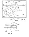
光学構成要素100は、導波路210、230および250に対して基板200上で(動作上容認可能な許容誤差の範囲内で)十分に正確な受動的位置決めを可能とすべく、一方では光学アセンブリの企図された機能性を可能とすべく適合化され得る。図5A、図5B、図5Cおよび図5Dには、基板200上で(たとえば導波路250等の)平面導波路の端面の近傍に適切に載置された構成要素100の実施例が示される。光学構成要素100は、各々の側壁108と、水平部材101と、当該光学構成要素100を形成する端壁との間に部分的に取り囲まれたポケットもしくは内側体積の部分106を形成すべく空間選択的に処理された構成要素基板上に形成されたものとして示される。この好適実施例において光学構成要素100は、実質的に平坦で実質的に垂直な内側表面102および外側面104を含む。この例において内側体積106の他端は、開放されたままである。この例において、水平部材101は光学構成要素100および側壁108を越えて延在するが、これは必須ではない。
The
構成要素100を形成するために実質的に均質な材料を用いると、構成要素100内における実質的に均一な光学特性に帰着し、また一方で、(空間的不連続性、勾配および/または変調の1つ以上を有する)不均質な材料を用いると、構成要素100内における同様に不均質な特性に帰着する。構成要素100、水平部材101および側壁108は、基板材料の空間選択的処理により形成され得る。代替的に、基板に対して1種類以上の異なる材料からなる上側層が形成されかつ空間選択的に処理されることで構成要素100および側壁108が形成され得るが、この場合には、水平部材101は、基板材料および上側層材料の一方もしくは両方を有する。光学構成要素100は、導波路210、230および250の各端部間の過剰な分離を必要とせずに構造的一体性を維持すべく、実施可能なだけ薄寸とされ得る。構成要素100の厚みは典型的には、約10μm乃至約50μm、多くの場合には約20μm乃至約30μmの範囲に亙り得る。十分に堅牢な材料から作製されると共に十分な注意を以て取り扱われるなら、さらに薄寸の光学構成要素が採用され得る。また、特定の光学機能性を実現すべく、かつ/または、2つの構成要素表面からの反射ビームをオフノーマル入射(off-normal incidence)形態で側方にオフセットすべく、必要もしくは好適であれば、(100μm以上の)さらに厚寸な光学構成要素100が採用され得る。表面102、104の一方もしくは両方は、光学機能性を提供する光学被覆を備え得る。導波路基板200上の対応する整列用構造/支持構造に係合すべく、側壁108および/または水平部材101上の1個以上の整列用縁部および/または垂直および/または水平整列表面、対応してマークされた導波路基板200上で構成要素100の視覚的位置決めを可能とする1個以上の整列マーク124、および/または、基板200に対して構成要素100を固定する1個以上の半田パッド123の内の1つ以上を提供すべく、空間選択的な材料処理が採用され得る。
Using a substantially homogeneous material to form
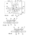
作製後、光学構成要素100を自身上に備えた水平部材101は反転され、基板200上に配置され、かつ、(図7A、図7B、図8Aおよび図8Bに示された如く)いわゆる「フリップチップ(flip-chip)」取付法を用いて当該基板に固定される。依然として光学構成要素100を収容しながら導波路210、230および250の各端部を分離する距離を減少(させて、存在し得る回折的な端部結合損失を幾分か緩和)すべく、かつ、基板200上における当該光学構成要素の取り付け/支持を確実とすべく、各平面導波路の内の1つの平面導波路(図示の例では導波路250)の少なくとも一方の端部は基板200の近傍領域から突出する隆起部を形成し得ることから、基板200上へと光学構成要素100をフリップチップ取付法により取り付けする際に導波路250の端部はポケット106内に受容され、光学構成要素100の表面104は導波路250の端面251の近傍とされる(図6A、図6B、図6Cおよび図6D)。ポケットもしくは内側体積の部分106は、約10μmから数十μm以上の高さの範囲に亙ることで典型的な平面導波路を収容し得ると共に、平面導波路を収容するに必要な任意の適切な幅を以て作成され得る。ポケット106の幅、および/または、その側壁108の位置/配向は、(図6A、図6B、図6C、図6D、図7A、図7B、図8Aおよび図8Bに示された如く、動作上容認可能な許容誤差の範囲内で)導波路250に対し(それゆえに、導波路210、230に対しても)必要な角度にて光学構成要素100の載置を許容すべく構成され得る。各導波路間における構成要素100の取り付けを促進しながら回折損失を減少すべく、上記各導波路は基板上に位置決めされることから、光学構成要素100の取り付け時に、導波路の端面の各々は対向する構成要素表面102もしくは104の約5μm以内である。導波路の端面と光学構成要素の表面との間をさらに離間することもまた、本願明細書の開示内容および/または添付の特許請求の範囲の各請求項の範囲内に納まり得る。
After fabrication, the
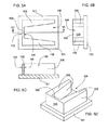
図6Aは、構成要素100に関して実質的に直交入射となり、導波路の端面もまた実質的に直交入射である光学構成要素の例を示している。図6Bは、実質的に直交する導波路端面を備えた非直交の光学構成要素を示している。導波路210、230および/または250の端面は、各導波路間の過剰な分離なしで非直交の光学構成要素100の接近した位置決めを可能とすべく適合化され得る。図6C、図6D、図7A、図7B、図8Aおよび図8Bの例において、各端面は角度付けがなされる(すなわち、夫々の導波路の伝搬方向に対して実質的に直交していない)ことから、非直交の光学構成要素100は各導波路の端面に対してさらに接近して位置決めされ得る。
FIG. 6A shows an example of an optical component that is substantially orthogonal with respect to
(導波路および光学構成要素が同様の屈折率であるときに)導波路の端面と構成要素100の名目上の一切の非反射表面とにおける不要な反射損失を減少するために、導波路端面と上記光学構成要素の表面との間には、屈折率が整合した埋設媒体が介設され得る。このことは、組み立てられた導波路および光学構成要素を、ポリマ等の実質的に屈折率が整合した埋設媒体内に埋設することで達成され得る。各光学的表面間の空間内には、ポリマ前駆体の溶液もしくは懸濁液が付与されて当該空間内へと流れる。ポリマの硬化後、導波路および光学構成要素および導波路が埋設される。上記光学構成要素の内側面104と、当該光学構成要素のポケット内に受容された導波路の端面との間における屈折率整合(すなわち「充填(potting)」)材料の流れを促進するために、端壁上にて構成要素100の回りで一方もしくは両方の側壁108を貫通して、かつ/または、構成要素基板101を貫通して1個以上の開口が形成され得る。導波路および構成要素の材料が相当に異なる屈折率を有しているとしても、埋設材料によれば依然として(空気もしくは真空に対する)不要な反射損失が減少し得る。
To reduce unwanted reflection losses at the waveguide end face and any nominally non-reflective surface of the component 100 (when the waveguide and optical component are of similar refractive index), the waveguide end face Between the surface of the optical component, an embedded medium having a matching refractive index can be interposed. This can be achieved by embedding the assembled waveguide and optical components in a substantially refractive index matched embedded medium such as a polymer. A polymer precursor solution or suspension is applied in the space between the optical surfaces and flows into the space. After curing of the polymer, the waveguide and optical components and waveguide are embedded. To facilitate the flow of refractive index matching (ie, “potting”) material between the
もし、透過結合式端部伝達のみが企図されるならば、本願明細書中に開示された如く作製された光学構成要素は(図6Aに示された)直交もしくは略直交入射にて採用され得るが、非直交入射も採用され得る。透過的光学機能性のみが必要とされ得る光学構成要素としては、どこにも導向されることが必要でない1つ以上の入射スペクトル成分を阻止することが企図された、たとえばスペクトル的なノッチ、短ギャップ、長ギャップおよび/または帯域通過フィルタが挙げられる。かかる機能性は、光学構成要素100の表面102および104の一方もしくは両方上の一層以上の光学被覆により容易に提供され得る。透過のみの光学構成要素の他の例は、本願明細書の開示内容および/または添付の特許請求の範囲の各請求項の範囲内に納まり得る。反射結合式端部伝達を含むためには典型的に、(図6B、図6C、図6D、図7A、図7B、図8Aおよび図8Bに示された如く)構成要素100に関して非直交入射が必要とされ得る。かかる構成要素は一例として本願明細書中で前述された種々のスペクトル・フィルタ形式を包含することが可能であり、その場合に阻止されたスペクトル成分は特定の箇所へと導向されねばならない。透過的および反射的な光学機能性の他の例は、本願明細書の開示内容および/または添付の特許請求の範囲の各請求項の範囲内に納まり得る。
If only transmissive end transmission is contemplated, optical components made as disclosed herein may be employed at normal or near normal incidence (shown in FIG. 6A). However, non-orthogonal incidence may also be employed. Optical components that may require only transmissive optical functionality are intended to block one or more incident spectral components that do not need to be directed anywhere, such as spectral notches, short gaps, etc. Long gap and / or band pass filters. Such functionality can be readily provided by one or more optical coatings on one or both of the
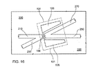
光学構成要素100により反射され、透過されかつ/または散乱された不要な光の少なくとも一部は、抑制することが好適であり得る。たとえば、導波路230から出射して光学構成要素100から導波路210内へと反射される光の一部は、構成要素100を通して漏出し得る。導波路230および250が角度的に非整列であるとすれば、多くの場合、この透過された不要な光の相当量が導波路250に進入する可能性は少ない。ただし、それでも、かかる漏出光が基板200上の他の構成要素もしくはデバイスに到達する量を減少することは好適であり得る。側壁108は、たとえば導波路230から構成要素100を介して透過された上記の不要な光(構成要素100の動作波長におけるもの)を吸収すべく適合化され得る。代替的に、図7Cおよび図8Cに示された如く側壁108は、上記の不要な透過光を下方へと基板200内に反射すべく、吸収させるべく、または、基板表面上の構成要素から離間させて透過すべく、傾斜されまたは適切に被覆され得る。これらの適合化は、導波路250から出射して構成要素100から反射される不要な光を抑制し、構成要素100を通して導波路210内へと透過させる役割も果たし得る。代替的に、図16に示された如く基板200上には、(夫々導波路230および250から)透過もしくは反射された不要な光信号を受信すべく付加的導波路270が配置され得る。かかる「ビームダンプ(beam dump)」導波路は、基板200上の繊細な構成要素から不要な光を取り去り得るか、または、不要な光を吸収もしくは消散すべく任意の適切な様式で適合化され得る。図16の好適実施例は4ポート光学アセンブリを実現するためにも採用可能であり、その場合に導波路210、230、250および/または270のいずれかもしくは全てが、構成要素100により反射および/または透過された光信号を透過しかつ/または受信すべく使用され得ることを銘記されたい。
It may be preferred to suppress at least some of the unwanted light reflected, transmitted and / or scattered by the
反射結合式端部伝達は、光学構成要素100上の任意の適切な入射角にて実施され得る。多くの光学被覆および/または構成要素は、入射角により変化する特性であって、波長および/または偏光への依存性を有する一方で(収束するもしくは発散する入射ビーム内に存在する入射角の範囲によりさらに複雑にされるという)入射角に依存する特性を呈する。これらの依存性は典型的には、直交入射の近傍にては最小であると共に入射角が増大すると共に大きくなり、一定の場合には、所定の光学構成要素100に対して使用され得る入射角に対する上限値が課され得る。使用可能な入射角に対する下限値は部分的に、上記光学アセンブリにおいて許容され得る回折損失の度合いにより決定され得る。図7Aおよび図8Aにおいて、導波路210および230は構成要素100に接近するにつれて合流して示される。寄生的な光学損失は、各導波路の合流部分の長さが増大するにつれて大きくなる一方、入射角が減少するにつれて(それゆえに、各導波路間の分離角度が減少するにつれて)大きくなる。所定の任意のアセンブリにおいて(大きな入射角により劣化され得る)必要な光学性能は、各導波路の合流部分により引き起こされる(典型的には、入射角が小さいほど悪化する)光学損失に対して平衡化され得る。導波路基板に対しては、幾何的および空間的な制約もまた関与し得る。光学構成要素100を介して特定の光学機能性を取入れる特定の光学アセンブリに対しては典型的に、所定範囲の折衷的な値が利用可能である。多くの光学アセンブリは、約45°未満(すなわち、約90°未満の角度を形成すべく反射結合された導波路同士)、多くの場合には約7°乃至約18°(すなわち、約15°乃至約35°の角度を形成すべく反射結合された導波路同士)の入射角を有し得る。ただし、光学構成要素100に対する任意の適切な入射角(および反射結合された導波路同士間の対応角度)は、本願明細書の開示内容および/または添付の特許請求の範囲の各請求項の範囲内に納まり得る。
The reflective coupled end transmission can be performed at any suitable angle of incidence on the
図15A乃至図15Cに示された如く光学構成要素100に対する小さな入射角における光学損失を減少させるために、薄寸の(すなわち、約3μmより低い高さ、多くの場合には約1μmより低い高さの)コアを有する導波路が採用され得る。コア212および232の一方の存在により他方における寄生的な光学損失が生じるが、この寄生損失は干渉コアの断面積に概ね比例する。導波路210および230によりサポートされる所定の光学モードのサイズに対し、コア212および232の断面積が減少すると、一方のコアにより引き起こされる他方のコアからの寄生的な光学損失のレベルは対応して減少する。また導波路同士間における所定の角度に対し、(図15Cの断面に示された如く)薄寸の導波路コアを使用すると、(図15Bの断面に示された)さらに厚寸な方の導波路コアに対する寄生的な光学損失が減少する。たとえば、20°だけ分離された導波路同士に対しては、高さおよび幅が約6〜7μmの各コアは約0.8dB以上の光学損失を呈し得る。対照的に、同一の分離角度に対し、約0.5μmの高さで約5μm幅の各コアは約0.2dBのみの光学損失を呈し得る。さらに、各コア間の鋭角をさらに完全でさらに均一なクラッド材料で充填すると、(クラッド材料の再流動を達成するための高温もしくは付加的な処理段階を必要とせずに)さらに厚寸なコアに対して薄寸コアでは光学損失がさらに減少し得る。
In order to reduce optical losses at small angles of incidence for the
図9には、光学構成要素100により提供される多重機能性の例が示される。この例において、構成要素100は、平面導波路210からの入射光信号(入射光ビーム10)の(λ1近傍の)第1スペクトル成分を平面導波路230へと導向し(反射光ビーム30)、かつ、平面導波路210からの入射光信号の(λ2近傍の)第2スペクトル成分を平面導波路250に対して透過する(透過光ビーム50)というスペクトル・フィルタとして作用し得る。表面102は、(λ1近傍の)第1スペクトル成分を実質的に反射する一方で(λ2近傍の)第2スペクトル成分を実質的に透過してスペクトル・フィルタ機能性を提供するための適切でスペクトルに対し選択的な反射被覆を備え得る。表面104は、必要であればまたは好適であれば、(λ2近傍の)適切な反射防止被覆を備え得る。これに加えて表面102および/または104は、導波路210および230の間または導波路210および250の間における端部結合を改善するために(図9では水平次元においてのみ示されるが、一方もしくは両方の次元における)曲率を備え得る。図9の好適実施例において表面102は、凹状表面として示される。表面102の曲率は、入射光ビーム10を受信すると共に発散性が減少しまたは所定度合いの収束性を備えた反射光ビーム30を生成することで導波路210および230間の端部結合を改善するための焦点合わせミラーとして作用すべく設計され得る。湾曲表面102は、導波路210および230を実質的にモード整合させるべく設計され得る。表面104の曲率は、構成要素100が湾曲表面102および104により、入射光ビーム10を受信すると共に発散性が減少しまたは所定度合いの収束性を備えた透過光ビーム50を生成することで導波路210および250間の端部結合を改善するための焦点合わせレンズ(この例ではメニスカス・レンズ(meniscus lens))として作用するように設計され得る。湾曲表面102および/または104は、導波路210および250を実質的にモード整合させるべく設計され得る。湾曲表面102および/または104に加えて構成要素100は、透過光ビーム50の焦点合わせを提供する屈折率勾配材料(index-gradient material)を含み得る。もし、反射ビーム30が表面102の代わりに表面104から反射されるならば、両方の湾曲表面ならびに一切の屈折率勾配は、導波路210および230間のモード整合に影響する。
In FIG. 9, an example of the multi-functionality provided by the
光学構成要素100によれば、本願明細書の開示内容および/または添付の特許請求の範囲の各請求項の範囲内に納まる他の多くの特定の光学機能性が単独でもしくは種々の組み合わせで提供され得る。かかる機能性は、構成要素100および/またはその表面102および104の一方もしくは両方を適切に適合化することで提供され得る。限定的なものとしてではなく、かかる機能性の例としては、スペクトル・フィルタリング、(空間的および/または時間的な)スペクトル分散、スペクトル操作(振幅および/または位相)、空間的操作(振幅および/または位相)、減衰、焦点合わせ、デフォーカス、光線平行化、モード整合、偏光選択(直線および/または円)、偏光遅延(直線および/または円)、偏光操作、光学的分離、絞り、ビネット(vignetting)、ビームスプリット、ビーム結合、多重化、多重分離、双方向受信/送信等が挙げられる。
The
図10Aおよび図10Bには、各々が双方向光学送受信機として機能すべく配置された代表的な光学アセンブリが示される。送受信機基板400上には平面導波路410、430、450、460および470が配備される。(夫々がλ1およびλ2の近傍にて中心合わせがなされて)到来する2つの波長多重光信号は、導波路410に対して端部結合がなされた光ファイバ490から上記双方向送受信機に進入する。光ファイバ490は、当該光ファイバを導波路410に対して位置決めする基板400上のV溝491内に受容される。導波路410および光ファイバ490は、横方向伝達(transverse-transfer)(米国特許出願公開公報第2003/0081902号に教示されたもの)および端部伝達などの任意の適切な手法による両者間の光パワー伝達に対して適合化され得る。典型的には、到来する光信号は未知で変動する偏光状態にて光ファイバ490の端部に到達するのが実情である。導波路470に対しては、変調されたレーザ光源480(λ3の近傍にて中心合わせがなされた光出力)が連結して示される。レーザ光源480の出力は、端部伝達もしくは横方向伝達等の任意の適切な手法で導波路470に対して伝達され得る。基板400上にてレーザ光源480を導波路470に対して位置決めして固定するために、レーザ光源480および基板400上には、(図10Aおよび図10Bでは図示されていない)支持/整列用構造および/または整列マークが形成され得る。
10A and 10B show exemplary optical assemblies that are each arranged to function as a bidirectional optical transceiver. On the
導波路410と450との間には、本願明細書中で前述された第1スペクトル・フィルタ412が配置される。図10Aにおいてフィルタ412は、第2到来光信号(λ2)およびレーザ出力信号(λ3)は実質的に透過する一方で第1到来光信号(λ1)は実質的に反射すべく設計され得る。導波路430は、反射された第1到来光信号を受信すると共に第1電気出力信号へと変換すべく当該第1到来光信号を光検出器436に対して伝達すべく配置され得る。導波路430における間隙内には、第1到来光信号(λ1)を実質的に透過する一方で第2到来光信号(λ2)を反射することで、スペクトル・フィルタ412からの第2到来光信号(λ2)の望ましくない反射から光検出器436を分離するための第2および第3スペクトル・フィルタ432および434が配備され得る。適切な性能特性(帯域幅、波長応答等)を有する任意の光検出器が採用され得る。導波路450と470との間には第4スペクトル・フィルタ452が配備され、当該フィルタは、レーザ出力信号(λ3)を実質的に透過する一方で第2到来光信号(λ2)を実質的に反射すべく設計され得る。導波路460は、反射された第2到来光信号を受信すると共に第2電気出力信号へと変換すべく該光信号を光検出器466に伝達すべく配置され得る。他の光信号(λ1および/またはλ3)から光検出器466を実質的に分離するために、必要ならまたは所望であれば、導波路460に沿い付加的なスペクトル・フィルタが配備され得る。適切な性能特性(帯域幅、波長応答など)を有する任意の光検出器が採用され得る。レーザ出力は、導波路470に沿い、スペクトル・フィルタ452を通過し、導波路450に沿い、スペクトル・フィルタ412を通過し、導波路410に沿い、かつ、光ファイバ490内へと送信される。一定の場合にはスペクトル・フィルタ412および452からの出力光信号の不都合な反射は(出力信号の全体的な減衰以外には)殆ど影響がないこともある。なぜならば、上記反射は上記送受信機上の他の構成要素もしくはデバイスに影響する方向ではないからである。必要ならまたは所望であれば、フィルタ412および452は(本願明細書中に記述された如き)出力光信号の不要な反射を吸収もしくは方向変換すべく適合化され得るか、または、(本願明細書中に記述された如き)かかる不要な反射光を受信する付加的な単一もしくは複数の導波路が基板400上に配備され得る。
Between the
図10Bにおいてフィルタ412は、第1到来光信号(λ1)を実質的に透過する一方で第2到来光信号(λ2)およびレーザ出力信号(λ3)は実質的に反射すべく設計され得る。導波路450は、透過された第1到来光信号を受信すると共に第1電気出力信号へと変換すべく当該第1到来光信号を光検出器436に対して伝達すべく配置され得る。導波路450における間隙内には、第2到来光信号(λ2)およびおそらくは出力光信号(λ3)も反射する一方で第1到来光信号(λ1)を実質的に透過することで、スペクトル・フィルタ412を通る他の光信号(λ2および/またはλ3)の一切の不都合な透過から光検出器436を実質的に分離するための第2および第3スペクトル・フィルタ452、454が配備され得る。適切な性能特性(帯域幅、波長応答等)を有する任意の光検出器が採用され得る。導波路430と460との間には第4スペクトル・フィルタ432が配備され、当該フィルタは、第2到来光信号(λ2)を実質的に透過する一方でレーザ出力信号(λ3)を実質的に反射すべく設計され得る。導波路460は第2到来光信号(λ2)を、第2電気出力信号へと変換するために光検出器466へと伝達する。必要ならまたは所望であれば、他の光信号(λ1および/またはλ3)から光検出器466を実質的に分離するために導波路460に沿い付加的なスペクトル・フィルタが配備され得る。適切な性能特性(帯域幅、波長応答など)を有する任意の光検出器が採用され得る。レーザ出力信号(λ3)は、導波路470に沿って透過され、スペクトル・フィルタ432から反射され、導波路430に沿って透過され、スペクトル・フィルタ412から反射され、導波路410に沿って光ファイバ490内へと透過する。必要ならまたは所望であればフィルタ412および432は(本願明細書中に記述された如き)出力光信号の不要な透過を吸収もしくは方向変換すべく適合化され得るか、または、(本願明細書中に記述された如き)かかる不要な透過光を受信する付加的な単一もしくは複数の導波路が基板400上に配備され得る。
In FIG. 10B, the
図10Aおよび図10Bの構成またはその変形例のいずれが採用されるかは、上記レーザおよび/または光検出器に対して必要とされるレベル分離、低い到来信号レベル、検出効率、レーザ出力パワー、デバイスサイズ制約等の種々の要因に依存し得る。これらの実施例は、本願明細書の開示内容および/または添付の特許請求の範囲の各請求項の範囲内で平面導波路および光学構成要素を用いて実現され得る多重構成要素式の光学デバイスの多くの例の内の2つにすぎない。 Which of the configurations of FIGS. 10A and 10B or variations thereof is adopted depends on the level separation required for the laser and / or photodetector, low incoming signal level, detection efficiency, laser output power, It may depend on various factors such as device size constraints. These embodiments of a multi-component optical device that can be implemented using planar waveguides and optical components within the scope of the disclosure and / or claims of the appended claims. Only two of many examples.
スペクトル・フィルタ412、432、434、452および454に対して採用された被覆のスペクトル的反射/透過特性は典型的には入射角により変化し、かつ、典型的には入射角が0°(すなわち直交入射)から増大するときにSおよびP入射偏光に対して異なる。到来光信号は典型的には良好に規定されながらも未知の偏光状態にて光ファイバ490を通して到達し、かつ、これらの偏光状態は時間と共に未知様式で変化し得る(到来信号はおそらく、光通信システムを通る異なる経路を異なる回数だけ踏破している)。スペクトル・フィルタ412、432、434、452および454の性能におけるこの偏光可変性の影響は、十分に小さな入射角を選択することで、動作上容認可能なレベルにてまたはそれより低く維持され得る。「十分に小さな」とは典型的に、特定のデバイスに対する特定の性能要件に依存する。たとえば、波長λ1、λ2およびλ3が十分に広く分離されれば、さらに接近して離間された波長の場合よりも広範囲な入射角が許容され得る。上記の各導波路および各スペクトル・フィルタの幾何的配置は典型的に、最小の入射角を必要とする。上記好適実施例においてスペクトル・フィルタ432、434(図10A)または452、454(図10B)は直交入射近傍に配置され(ることで偏光に依存する性能を実質的に減少させ)得る。なぜならば、それは反射波長を阻止することのみを必要とするからである。スペクトル・フィルタ412、452(図10A)または412、432(図10B)は典型的にオフノーマル入射を必要とする。なぜならば、反射波長は別の導波路へと導向されねばならないからである。これらのオフノーマルのスペクトル・フィルタに対する入射角は典型的には、偏光に依存する性能変動を動作上容認可能な限度内に維持するのに十分なほど小さく、かつ、各導波路の適切な幾何学形状に適応するに十分なほど大きく選択される。上記好適実施例(反射結合された導波路同士間は約20°)においては約10°の入射角が示されるが、これらの形式の双方向アセンブリにおいて反射結合された導波路同士間の角度は典型的には、約15°乃至約35°の範囲に亙り得る。入射角に対する特定の上限値および下限値は典型的には、本願明細書の開示内容および/または添付の特許請求の範囲の各請求項の範囲内に留まりながら、(一定の場合には上記で与えられた例示的範囲に含まれない)特定デバイスの詳細な性能仕様に依存して変化し得る。
The spectral reflection / transmission characteristics of the coatings employed for
図10Aおよび図10Bの好適実施例に示された如く、スペクトル・フィルタ432および434は共通の構成要素基板上に形成される。本願明細書中で上記された如く、2つの側壁と、2つの端壁と、水平部材とにより部分的に囲繞されたポケットもしくは内側体積の部分が形成される。各端壁は、本願明細書中に記述された如く透過的/反射的光学構成要素の役割を果たし得ると共に、上記ポケットは自身内に導波路セグメントを収容し得る。それゆえに、取り囲まれた導波路セグメントは各端部にて、端壁を介して上記ポケットの外側の他の2つの導波路に対して透過結合され得る。かかる二構成要素基板(水平部材101上の構成要素100aおよび100b)およびその内部にて取り囲まれた導波路セグメント310は、必要に応じてもしくは所望であれば、直交もしくは非直交入射に対して適合化され得る(図11Aおよび図11B)。もし、導波路310の各端部と構成要素100aおよび100bの内側面との間に埋設媒体が採用されるならば、一方もしくは両方の側壁を貫通して、上記光学構成要素の回りにおける一方もしくは両方の端壁を貫通して、かつ/または、水平部材101を貫通して1個以上の開口が形成され得る。かかる開口によれば、埋設媒体は内側体積の部分106に流入して各光学的表面間の空間を充填し得る。
As shown in the preferred embodiment of FIGS. 10A and 10B,
水平部材101上における光学構成要素100、内側体積106、側壁108および他の構造を形成すべく、種々の材料および作製技術が採用され得る。光学構成要素100の使用に対して企図された波長範囲に依存し、異なる材料が採用され得る。適切な材料としては、限定的なものとしてではなく、半導体(限定的なものとしてではなく、ケイ素、GaAs(ガリウム砒素、InP(インジウム燐)、他のIII−V族の半導体、および/または、半導体合金、および/または、酸化物が挙げられる)、結晶材料、シリカもしくはシリカ系材料、他のガラス、ポリマ、および、本願明細書中では明示されないが本願明細書の開示内容および/または添付の特許請求の範囲の各請求項の範囲内に納まり得るという他の多数の例が挙げられる。水平部材101および光学構成要素100の両方に対して単一の材料が採用され得るか、または、水平部材101に対しては1つの材料が採用されかつ当該水平部材上に光学構成要素100を形成すべく別の材料の上側層が使用され得る。
Various materials and fabrication techniques can be employed to form the
共通のウェハ上に複数の光学構成要素を同時に作製するために、ウェハ規模(wafer scale)で空間選択的処理が使用され得る。光学構成要素100は上記水平部材から突出し、かつ、表面102および/または104は実質的に平面的なウェハ(図12A、図12Bおよび図12C参照:一定の場合には非直交表面が容認可能もしくは好適であり得る)の表面に対して実質的に直交され得る。水平部材101および一切の水平な支持/整列表面は上記平面的基板ウェハにより規定される一方で、実質的に垂直な整列および/または光学的表面は空間選択的処理段階により規定される。表面102、104の品質は、それらを形成すべく使用される空間選択的段階の性質により決定される。使用される特定技術と、それが実施される正確な様式とに依存し、種々の度合いの表面品質が達成され得る。表面102、104を形成する一定の代表的な処理技術としては、限定的なものとしてではなく、(反応性イオン・エッチングなどの)ドライエッチング・プロセス、(結晶学的に規定された特定の表面に制限される)異方性湿式エッチング・プロセス、(結晶学的に規定された劈開平面に沿うものであり、基板ウェハは構成要素100と共に劈開されることから表面102に対してのみ適用可能とされ得る)劈開、および/または、精密切断機もしくは他の機械的切断用具による切断が挙げられる。
Spatial selective processing can be used at the wafer scale to simultaneously create multiple optical components on a common wafer.
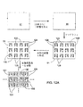
上記の「垂直な」表面102および/または104に対して形成される光学被覆は、一定の場合(図12Aおよび図12B)にはウェハ規模で形成され得る。たとえば、水平および垂直な表面の両方に対して実質的に均一な厚みで被覆を行うためには、いわゆる共形的(conformal)析出技術が使用され得る。図12Aにおいて被覆は、表面102および104の両方に対してこのように提供され(当該2つの表面に対して同一のまたは異なる被覆)、その後でウェハは個々の構成要素へと分割される。ウェハ規模基板が先ず、各々が単一列の複数の構成要素(図12Bおよび図12C)を自身上に有するという細長片もしくは「棒状体(bar)」へと切断されるなら、垂直な表面102、104に対して多様な被覆および被覆技術が適用され得る。図12Bにおいては、ウェハを棒状体へと分割する前に、ウェハ規模で表面104に対して共形的(conformal)被覆が形成される。棒状体へと分割した後、各棒状体は約90°反転されることから、表面102は被覆チャンバまたは他の材料析出装置に関して「水平」である。上記の各棒状体は、棒状体自体の表面102上に所望の被覆を析出した後で個々の構成要素へと分割され得る。図12Cにおいて、ウェハは一切の被覆が析出される前に棒状体へと分割される。棒状体へと分割された後、各棒状体は約90°反転され得ると共に、表面102もしくは104の一方には所望の被覆が形成され得る。各棒状体は次に約180°反転され得ると共に、所望の被覆(同一被覆もしくは異なる被覆)が表面102もしくは104の他方に形成され得る。上記被覆の形成後、各棒状体は個々の構成要素へと分割され得る。
The optical coating formed for the “vertical” surfaces 102 and / or 104 described above may be formed on a wafer scale in certain cases (FIGS. 12A and 12B). For example, so-called conformal deposition techniques can be used to provide a coating with a substantially uniform thickness on both horizontal and vertical surfaces. In FIG. 12A, coatings are thus provided for both
図5A、図5B、図5C、図5D、図6A、図6B、図6Cおよび6Dに示された好適実施例は、実質的に均質な単一の基板材料から形成された光学構成要素100、側壁108および水平部材101を有し得る。適切な基板材料としては、ケイ素、InPおよび/またはIII−V族の半導体、他の適切な半導体、半導体酸化物および/または合金、および/または、他の適切な材料が挙げられる。代替的に、構成要素100および側壁108は、たとえばシリコン基板上のシリカもしくはシリカ系上側層(他の上側層/基板の組み合わせが採用され得る)等の、(図12A、図12Bおよび図12Cにおける如き)基板91上の上側層90から形成され得る。上側層90は、実質的に均質な単一層からなることから実質的に均質な構成要素100に帰着し得るか、または、異なる材料の多重層からなることから構成要素100の光学特性の垂直方向の不連続性、勾配もしくは変調に帰着し得る。図12A、図12Bおよび図12Cには、代表的なプロセス図が示される。光学構成要素100のポケット106、側壁108の内側面、および表面104を形成するために、層90あるいは(上側層が存在しなければ)基板91の空間選択的エッチングが採用され得る。所望であれば、半田パッドなどの他の要素に加え、(図5A、図5B、図5C、図5D、図6A、図6B、図6Cおよび図6Dには示されないが、もし存在するなら)付加的な整列用構造/支持構造および/または整列マーク124もまた形成され得る。表面102は(ポケット106および/または支持構造および/または整列マーク124と同時にもしくは順次的に)空間選択的エッチングにより形成され得るか、または、表面102は精密切断機による切断に続き再流動もしくは徐冷段階もしくは他の一定の適切な平滑化段階(たとえば湿式エッチング段階)により提供され得るか、または、表面102は(構成要素100および水平部材101の両方を含む)ウェハを棒状体92へと精密劈開することで形成され得る。採用される空間選択的エッチング段階および/または切断機による切断は、(動作上容認可能な許容誤差の範囲内で)実質的に平坦で実質的に垂直な表面102、104を提供する様式で実施され得る。半導体の結晶面に制限されたエッチングもしくは劈開によれば、基板ウェハの配向性により可能とされる精度に従う表面が生成される。
The preferred embodiment shown in FIGS. 5A, 5B, 5C, 5D, 6A, 6B, 6C, and 6D includes an
形成されるべき光学構成要素の性質に依存して、いずれの場合にも動作上容認可能な許容誤差の範囲内で、表面102、104が実質的に平行とされること、または、それらの間で設計された楔角度(wedge angle)を形成することが好適であり得る。かかる楔角度は、エッチング、劈開および/または切断機による切断の処理段階を適切に空間制御することで水平次元により提供され得る。垂直次元における楔角度は、エッチング、劈開および/または切断機による切断の処理段階を適合化して所望の楔角度を形成することで達成され得る。上記の作製例においてはエッチングが示されたが、光学構成要素100を形成するためには、他の空間選択的な材料除去技術、空間選択的な材料析出技術、または、空間選択的な材料析出技術および除去技術の組み合わせも採用され得ることを銘記されたい。この点において、構成要素100の光学特性における任意の所望の水平方向の変化(横方向または長手方向)は、内側体積の部分106の端壁に対する適切な空間選択的処理により提供され得る。
Depending on the nature of the optical component to be formed, in any case, the
表面102および104が形成されて光学構成要素100に対する「半加工品(blank)」が形成されたなら、本願明細書中で上記された如く表面102、104の一方もしくは両方に対しては被覆が形成され得る。これらの被覆は、所望の機能性を提供する任意の適切な形式とされ得ると共に、かかる被覆を提供する任意の適切な方法により提供され得る。たとえば光学構成要素100は、ダイクロイック・ビームスプリッタまたはビーム結合器(すなわち、1つ以上の設計波長もしくは波長帯域においては実質的に反射的であり、1つ以上の他の設計波長もしくは波長帯域においては実質的に透過的であり、スペクトル・フィルタとも称され得る)を有する。必要とされる透過および反射のスペクトルおよび偏光特性は広範に変化し得ると共に、当該特性は、本願明細書の開示内容および/または添付の特許請求の範囲の各請求項の範囲内に留まりながら、構成要素100の企図用途およびそれに対する仕様、被覆を提供する設計および製造の能力、設計波長もしくは波長帯域の分離、入射角、および、入射光信号の偏光特性、ならびに、他の適切なパラメータにより決定され得る。かかるフィルタ被覆は、表面102および104のいずれかに対して形成され得る。必要でありまたは好適であれば、他の表面からの付加的な反射は、その上に適切な反射防止被覆を形成することで抑制され得る。不要な反射は、表面102および104間に楔角度を提供することで方向変換され得るか、または、オフノーマル入射形態で構成要素100に対して十分な厚みを提供することで側方に変位され得る(たとえば、約10°乃至15°の入射角にて約100μmの厚みの構成要素は十分に、導波路内への不要な反射の反結合(back-coupling)を典型的に抑制し得る)。もし、構成要素100および上記導波路が同様の屈折率(たとえばシリカ系の導波路および構成要素に対しては約1.4〜1.5)であれば、上記構成要素と上記導波路の端面とに対して屈折率整合媒体を埋設すると、反射防止被覆、楔角度および/または厚寸のオフセット構成要素に対する必要性が回避され得る。もし、構成要素100および上記導波路の屈折率が相当に異なるならば(たとえばシリカ系の導波路では1.4〜1.5であり、半導体系の化合物では2.9〜3.4である)、埋設媒体が採用されるか否かにかかわらず、構成要素100からの不要な反射を十分に抑制するためには反射防止被覆、楔角度および/または厚寸構成要素の1つ以上が必要とされ得る。
Once
本願明細書中において上記に言及された如く、ウェハ規模処理の間において表面102、104上には共形的析出技術を用いて被覆が形成され得るか、または、ウェハは、単一列の構成要素を備えた棒状体へと分割されると共に多様な被覆技術を用いて被覆され得る。本願明細書中に示された光学構成要素の一定の実施例は、非平行な側壁108を備えたポケット106を含む(すなわち、ポケット106は開放端部から光学構成要素に向けて狭幅となる)。これによって、光学構成要素はポケット106内における導波路に対して所望の入射角にて位置決めされ得ると記述されている。上記ポケットを拡げると、光学構成要素100の内側面104に対する光学被覆の形成も促進され得る。(図11Aおよび図11Bにおける如き)二重構成要素の基板に対しては、構成要素100a、100bの一方もしくは両方の内側面に形成される任意の被覆はウェハ規模処理の間において最も容易に形成されることも銘記されたい。この場合には、ウェハを棒状体へと分割しても、被覆を形成するために構成要素の内側面へのアクセスは改善されない。
As mentioned hereinabove, a coating may be formed on the
ウェハに対して実質的に直交して光学構成要素100を作製するための図12A、図12Bおよび図12Cの空間選択的処理段階は、共通のウェハ上に多数の構成要素(ウェハ毎に、数十、数百もしくは数千の構成要素)を同時的に作製するためにウェハ規模で実施され得る。このようにして、相当の経済的規模が実現され得る。既に指摘した如く、一定の製造段階はウェハ規模での実施に対しては適切でないこともあるが、依然として、個々の構成要素を操作せずに複数のデバイスに対して同時的に実施され得る。たとえば、(ウェハ表面に対して実質的に直交する)表面102もしくは104上に光学被覆を形成する一定のプロセス・シーケンスは、特に所望の被覆が複数の被覆層を含むならば、ウェハ規模で実施することは複雑なこともある。もし、被覆されるべき表面が、被覆装置の析出方向に対して実質的に直交するように配向されるならば、その表面はさらに容易に被覆され得るか、または、さらに複雑で精密な多重層被覆がさらに容易に形成され得る。(ウェハ規模処理段階の完了後に)ウェハを最初に1次元において劈開もしくは分割すると、各々が自身上に単一列の構成要素を備えたウェハの棒状体もしくは細長片が得られる。最初の分割は、被覆されるべき表面が棒状体の長手軸心に対して実質的に平行であるように行われ得る。次に必要に応じて、個々の構成要素を取り扱うのではなく各棒状体上の複数の構成要素に関して同時に、表面102および/または104に対して光学被覆が形成され得る。共通の被覆装置において複数の棒状体を同時に被覆することが可能であり得る。被覆が形成されたなら、各棒状体はさらに分割されて個々の構成要素が生成され得る。
The spatially selective processing steps of FIGS. 12A, 12B, and 12C to make the
本願明細書中で上記された如く構成要素100に対してさらに概略的な機能性を提供するために、(図12A、図12Bおよび図12Cに示された如き)プロセス・シーケンスの間において種々の技術が採用され得る。構成要素100の光学特性の垂直方向の不連続性、勾配および/または変調を提供するためには、種々の形式(超格子材料、量子井戸材料、ドープ材料、屈折率勾配材料等)の多重層、勾配もしくは変調材料が使用され得る。かかる材料は、光学構成要素100を形成すべく採用された空間選択的エッチングまたは他の空間選択的な材料除去により実質的に均一な一群の層として形成され得る。光学構成要素100を形成するために、異なる材料の一連の空間選択的析出が採用され得る。いずれの場合にも、多数の構成要素の同時的作製のためにウェハ規模処理が採用され得る。構成要素100の光学特性の水平方向の不連続性、勾配および/または変調を提供するために空間選択的な材料処理が採用され得ると共に、当該処理は同時的な多数の構成要素のためにウェハ規模で実施され得る。表面102および/または104に対して形成される被覆の空間的不連続性、勾配および/または変調は、共通の棒状体上で複数の構成要素に対して同時に実施され得るという任意の適切な空間選択的被覆および/または処理技術を用いて提供され得る。本願明細書中で上記においては、処理段階の空間的制御により表面102、104の水平配向の制御が記述されている。同様の様式にて、表面102、104の一方もしくは両方に対して曲線的および/または柱面的な水平プロフィルを提供するために、処理段階の空間的制御が採用され得る。かかる表面プロフィルは、空間選択的処理を適切に改変することで垂直次元においても提供され得る。たとえば、かかる垂直方向の表面プロフィルを形成するためには、多段階および/またはグレースケールのリソグラフィが採用されることもある。本願明細書の開示内容および/または添付の特許請求の範囲の各請求項の範囲内に留まりながら、企図された光学機能性を光学構成要素100に対して提供するためには、これらのおよび他の任意で適切な処理段階および/または適合化の内の任意の1つ以上が採用され得る。
In order to provide more general functionality for the
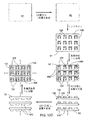
共通のウェハ上における複数の光学構成要素の同時的作製のためにウェハ規模の空間選択的処理が用いられ得るが、その場合に各光学構成要素100およびその表面102、104は、実質的に平面的なウェハ表面に対して実質的に平行である(図13Aおよび図13B参照:ここでは、「垂直な」光学構成要素の端壁は基板ウェハに対して平行に位置している)。空間選択的処理の間における上記のような配置の結果、これらの表面の光学的品質が改善され得ると共に、表面102および/または104に対して任意の所望の精度および/または複雑さの光学被覆がウェハ規模で形成可能とされ得る。代表的なプロセス・シーケンス(図13Aおよび図13B)においては、実質的に平面的なシリコン・ウェハ500に対して先ず、最終的には内側体積の部分106(および光学構成要素100)の端壁を形成する実質的に均一な上側層502が形成される。上側層502は、たとえばシリコン・ウェハ500上のシリカ、窒化ケイ素または酸窒化ケイ素を含む。基板500としては、InPまたは他の適切なIII−V族の半導体もしくは合金が等価的に採用され得ると共に、上側層502としてはInPまたは他のIII−V族もしくは合金もしくは酸化物が採用され得る。本願明細書の開示内容および/または添付の特許請求の範囲の各請求項の範囲内に留まりながら、任意の適切なウェハ材料上では他の実質的に均質な上側層が採用され得る。上側層502は代替的に、(構成要素100内における最終的な光伝搬方向に沿って材料を変化させて)光学機能性を提供する多重層材料を含む。上記上側層はパターン形成かつエッチングされることで、ウェハ500の露出領域により取り囲まれたポケット106の端壁として最終的に各々が機能する光学構成要素層504が残置され得る。もし、光学構成要素100の光学特性において横方向の変化が所望であれば、それを提供するために領域504の適切な空間選択的処理が採用され得る。表面102が湾曲されるべきであれば、当該湾曲表面はこの時点において、(一方もしくは両方の次元において)領域504の表面プロフィルを変更するグレースケール・リソグラフィまたは他の同様の技術を用いて提供され得る。
Wafer-scale spatially selective processing can be used for the simultaneous fabrication of multiple optical components on a common wafer, where each
次にウェハ500が処理されることで、構成要素層504の近傍にて当該ウェハを貫通する通路506が形成され得る。次にウェハ500は反転されて他側から処理されることで、構成要素層504の中央部分の背後から基板材料が除去される。構成要素層504の裏面側に適切な高品質の光学的表面を残置しながら領域504の(光学構成要素100の表面104となる)裏面側の中央部分からウェハ材料を完全に除去すべく、材料特異的エッチングが採用される。もし、湾曲表面104が所望されるならば、それはこの時点にて、グレースケール・リソグラフィまたは他の同様の技術を用いて構成要素層504の裏面側のプロフィルを(一方もしくは両方の次元にて)変更することで提供され得る。この段階の間において形成された概略的に垂直な基板側壁は、完成した光学構成要素における水平部材101の内側面と側壁108とを形成する。使用されるエッチング・プロセスおよび設計された幾何学形状に依存し、基板側壁は、実質的に垂直とされ(て実質的に平行な側壁108を生成し)得るか、または、角度付けられ(て本願明細書中において上記に示された如く広幅の開放端部を備えると共に光学構成要素100に向かい狭幅となる内側体積の部分106を生成し)得る。ウェハ500の裏面に対してはウェハ規模にて任意の所望の光学被覆が形成されることで、多数の光学構成要素の表面104に対する光学被覆が提供され得る。
Next, the
ウェハ500はもう一度反転され、ウェハの表面に対しては構成要素層504(最終的な光学構成要素100の表面102)を含む任意の所望の光学被覆がウェハ規模にて形成され得る。それゆえに、上記上側層の構成要素層領域504は光学構成要素100の「半加工品」を形成し、かつ、ウェハの表面および裏面に対してウェハ規模で形成された被覆は表面102および/または104に対する光学被覆の役割を果たす。ウェハ規模の処理が完了したなら、ウェハは個々の光学構成要素へと切断され得る(図13A)。ウェハ500を個々の光学構成要素へと分割するためには、たとえば精密切断機による切断が採用され得るか、または、他の精密切断もしくは劈開手順が採用され得る。ウェハを分割して生成された各表面は、完成された光学構成要素(図14A、図14B)における側壁108の(フリップチップ取り付け時の)外側面および底面を形成する。これらの外側面および底面の正確な位置および配向は、使用されるウェハ分割処置の精度により決定される。側壁108の外側面および/または底面は、(図7A、図7B、図8Aおよび図8Bにおける如き)導波路210、230および250の組立て時に基板200上で光学構成要素100を正確に位置決めする役割を果たし得る。この処理シーケンスから帰着する結果的な水平部材101は、個々の構成要素へと分離する前はウェハに対して実質的に直交することが指摘される。側壁108の底面上に(半田パッド123、整列マーク124、整列用縁部等の)整列用構造および/または組立て構造を形成するために、上記ウェハは各棒状体へと分割され、各棒状体は約90°反転され、かつ、所望の構造が上記側壁の底面上に形成され得る(図13B)。上記側壁の底部の処理が完了したなら、各棒状体は個々の構成要素へと分割され得る。
光学アセンブリの上記の好適実施例ならびに同様に実現される他の実施例においては、基板200上に配備される要素であって当該基板200上の平面導波路として実現される導波路210、230、250、V溝201、整列用縁部202、支持/整列用構造203、205、223、および/または、整列マーク204、224の内の任意のもの等の要素に対して(動作上容認可能な限度内で)十分に正確な相対的位置決めを達成するために、空間選択的な材料処理技術が採用され得る。同様に、別体の基板239上に配備される要素であって導波路230、支持/整列用構造233および/または整列マーク234などの要素に対して(動作上容認可能な限度内で)十分に正確な相対的位置決めを達成するために、空間選択的な材料処理技術が採用され得る。基板200(および当該基板上の構造)を作製するこれらの空間選択的処理段階は、共通のウェハ上に多数の基板(ウェハ毎に、数十、数百もしくは数千の基板)を同時的に作製するためにウェハ規模で実施され得る。このようにして、相当の経済的規模が実現され得る。ウェハを個々の基板200へと分割した後、当該基板上には、必要な一切の光学構成要素100、別体の導波路、光検出器、光ファイバ等が配置されて固定され、機能的光学アセンブリが提供され得る。種々の溝、整列用縁部、支持/整列用構造、整列マーク等によれば、企図された光学アセンブリの光学機能性を実現するために(動作上容認可能な許容誤差の範囲内で)十分に正確な受動的組立てが容易に可能とされる。
In the above preferred embodiment of the optical assembly as well as other embodiments realized in the same way,
上記の記述説明および/または添付の特許請求の範囲の各請求項の目的に対し、本願明細書中で採用された「光導波路」(または等価的に「導波路」)という語句は、1つ以上の光学モードをサポートし得る構造を表現するものとする。かかる導波路は典型的に、長手次元に沿う伝搬を許容しながら、2つの横次元において、サポートされた光学モードの局限を提供するものとする。湾曲された導波路に対して横次元/方向および長手次元/方向は局所的に規定されるべきことから、たとえば曲線的な導波路の長さに沿って横次元および長手次元の絶対的配向は変化し得る。光導波路の例としては、限定的なものとしてではなく、種々の形式の光ファイバおよび種々の形式の平面導波路が挙げられる。本願明細書中で採用された「平面的光導波路」(または等価的に「平面導波路」)という語句は、実質的に平面的な基板上に形成された一切の光導波路を表現するものとする。上記長手次元(すなわち伝搬次元)は、基板に対して実質的に平行と見做されるものとする。基板に対して実質的に平行な横次元は横手もしくは水平次元と称され得る一方、基板に対して実質的に直交する横次元は垂直次元と称され得る。かかる導波路の例としては、リッジ(ridge)型導波路、埋設型導波路、半導体導波路、他の高屈折率導波路(「高屈折率」は約2.5より大きい)、シリカ系導波路、ポリマ導波路、他の低屈折率導波路(「低屈折率」は約2.5より小さい)、コア/クラッド型導波路、多重層リフレクタ(MLR)導波路、金属クラッド導波路、空気案内式導波路、真空案内式導波路、光結晶系もしくは光バンドギャップ系導波路、電気光学的(EO)および/または電気吸収的(EA)材料を取り入れた導波路、非線形光学(NLO)材料を取り入れた導波路、および、本願明細書中で明示的には示されないが本願明細書の開示内容および/または添付の特許請求の範囲の各請求項の範囲内に納まり得る他の多数の例が挙げられる。また一方で、半導体、結晶、シリカまたはシリカ系、他のガラス、セラミック、金属、および、本願明細書中で明示的には示されないが本願明細書の開示内容および/または添付の特許請求の範囲の各請求項の有効範囲内に納まり得る他の多数の例等の、多くの適切な基板材料が採用され得る。 For the purpose of each claim in the above description and / or appended claims, the phrase “optical waveguide” (or equivalently “waveguide”) employed herein is one A structure capable of supporting the above optical modes shall be expressed. Such waveguides typically provide localized optical modes in two transverse dimensions while allowing propagation along the longitudinal dimension. Since the transverse dimension / direction and the longitudinal dimension / direction should be defined locally for a curved waveguide, for example, the absolute orientation of the transverse and longitudinal dimensions along the length of the curved waveguide is Can change. Examples of optical waveguides include, but are not limited to, various types of optical fibers and various types of planar waveguides. As used herein, the phrase “planar optical waveguide” (or equivalently “planar waveguide”) refers to any optical waveguide formed on a substantially planar substrate. To do. The longitudinal dimension (ie propagation dimension) is assumed to be substantially parallel to the substrate. A lateral dimension that is substantially parallel to the substrate may be referred to as a transverse or horizontal dimension, while a lateral dimension that is substantially orthogonal to the substrate may be referred to as a vertical dimension. Examples of such waveguides include ridge waveguides, buried waveguides, semiconductor waveguides, other high refractive index waveguides (“high refractive index” is greater than about 2.5), silica-based waveguides. Waveguides, polymer waveguides, other low refractive index waveguides (“low refractive index” is less than about 2.5), core / clad waveguides, multilayer reflector (MLR) waveguides, metal clad waveguides, air Guided waveguides, vacuum guided waveguides, photonic crystal or optical bandgap waveguides, waveguides incorporating electro-optic (EO) and / or electroabsorptive (EA) materials, non-linear optics (NLO) materials And many other examples that are not expressly set forth herein and may fall within the scope of the claims of the specification and / or the appended claims. Is mentioned. On the other hand, semiconductors, crystals, silica or silica-based, other glasses, ceramics, metals, and disclosures and / or appended claims that are not explicitly indicated in the present specification. Many suitable substrate materials may be employed, such as numerous other examples that may fall within the scope of the following claims.
本願明細書中に開示された光学構成要素と共に適切に使用され得る平面的光導波路の1つの代表的な形式は、いわゆるPLC(平面光波回路)導波路である。かかる導波路は典型的には、実質的に平面的なシリコン基板上に(多くの場合にはシリカもしくはシリカ系の光学緩衝層が介設されながら)シリカもしくはシリカ系の導波路(多くの場合にはリッジ型導波路もしくは埋設型導波路であるが、他の導波路形態も採用され得る)を有する。1種類以上のかかる導波路の一群は、平面導波路回路、光学的集積回路、または、光電気的集積回路と称され得る。1個以上のPLC導波路を備えたPLC基板は、適切に適合化されたPLC導波路による光パワーの端部伝達に対して適合化された1個以上の光源、レーザ、変調器および/または他の光学デバイスの取り付けに対して容易に適合化され得る。1個以上のPLC導波路を備えたPLC基板は、1個以上の光源、レーザ、変調器、光検出器、および/または、適切に適合化されたPLC導波路による光パワーの横方向伝達(モード干渉結合もしくは実質的に断熱的な横方向伝達:横方向結合とも称される)に対して適合化された他の光学デバイスの取り付けに対して(米国特許出願公開公報第2003/0081902号および/または米国仮出願第60/466,799号の教示に従い)容易に適合化され得る。適切に適合化された1個以上のPLC導波路と共に、本願明細書中に開示された反射的および/または透過的な光学構成要素が容易に採用され得る。 One typical form of planar optical waveguide that can be suitably used with the optical components disclosed herein is a so-called PLC (planar lightwave circuit) waveguide. Such waveguides are typically silica or silica-based waveguides (often with a silica or silica-based optical buffer layer interposed, often on a substantially planar silicon substrate). Are ridge-type waveguides or buried-type waveguides, but other waveguide configurations may be employed). A group of one or more such waveguides may be referred to as a planar waveguide circuit, an optical integrated circuit, or an opto-electric integrated circuit. A PLC substrate with one or more PLC waveguides is one or more light sources, lasers, modulators and / or adapted for end transmission of optical power through appropriately adapted PLC waveguides. It can be easily adapted for the attachment of other optical devices. A PLC substrate with one or more PLC waveguides can transmit optical power laterally by one or more light sources, lasers, modulators, photodetectors and / or appropriately adapted PLC waveguides ( For the mounting of other optical devices adapted for modal interference coupling or substantially adiabatic lateral transmission (also called lateral coupling) (US 2003/0081902 and (Or according to the teachings of US Provisional Application No. 60 / 466,799). The reflective and / or transmissive optical components disclosed herein can be readily employed with one or more appropriately adapted PLC waveguides.
上記の記述説明および/または添付の各請求項の目的に対し、「空間選択的な材料処理技術」とは、エピタキシ、層成長、リソグラフィ、フォトリソグラフ、気化析出、スパッタリング、蒸着、化学蒸着、ビーム析出、ビーム支援式析出、イオンビーム析出、イオンビーム支援式析出、プラズマ支援式析出、湿式エッチング、乾式エッチング、イオン・エッチング(反応性イオン・エッチングを含む)、イオン・ミリング(ion milling)、レーザ加工、スピン析出、噴霧析出、電気化学的なメッキまたは析出、化学メッキ、フォトレジスト、紫外線(UV)硬化および/または緻密化、精密切断機および/または他の機械的な切断/成形工具を用いるマイクロ加工、選択的金属化および/または半田析出、平面化のための化学機械研磨、他の任意で適切な空間選択的な材料処理技術、それらの組み合わせ、および/または、それらの機能的均等物を包含するものとする。特に、層もしくは構造の「空間選択的な配備」を含む一切の段階は、(所定領域の全体に亙る)空間選択的な析出および/または成長、または、実質的に均一な析出および/または成長のいずれかまたは両方、および、それに続く空間選択的な除去を包含し得ることを銘記されたい。一切の空間選択的な析出、除去または他のプロセスは、いわゆる直接描画プロセスとされ得るか、または、マスク・プロセスとされ得る。本願明細書中で言及される一切の「層」は、実質的に均質な材料層を含むか、または、不均質な一層以上の一群の材料下位層を含むことを銘記されたい。。空間選択的な材料処理技術は、共通の基板ウェハ上に複数の構造を同時に作製/処理するためにウェハ規模で実施され得る。 For the purposes of the above description and / or the appended claims, “spatial selective material processing techniques” refers to epitaxy, layer growth, lithography, photolithography, vapor deposition, sputtering, vapor deposition, chemical vapor deposition, beam Deposition, beam assisted deposition, ion beam deposition, ion beam assisted deposition, plasma assisted deposition, wet etching, dry etching, ion etching (including reactive ion etching), ion milling, laser Using processing, spin deposition, spray deposition, electrochemical plating or deposition, chemical plating, photoresist, ultraviolet (UV) curing and / or densification, precision cutting machines and / or other mechanical cutting / forming tools Micromachining, selective metallization and / or solder deposition, chemical mechanical polishing for planarization, other optional Appropriate space-selective material processing techniques, combinations thereof, and / or functional equivalents thereof are intended to be included. In particular, any stage involving “spatial selective deployment” of layers or structures may include spatially selective deposition and / or growth (across a given area) or substantially uniform deposition and / or growth. It should be noted that either or both of these and subsequent spatial selective removal may be included. Any spatially selective deposition, removal or other process can be a so-called direct writing process or a mask process. It should be noted that any “layer” referred to herein includes a substantially homogeneous material layer or includes a group of one or more groups of material sub-layers that are heterogeneous. . Spatial selective material processing techniques can be implemented on a wafer scale to simultaneously create / process multiple structures on a common substrate wafer.
本願明細書中において基板上に「固定され」、「接続され」、「取り付けられ」、「析出され」、「形成され」、「配置される」等の種々の構成要素、要素、構造および/または層は、基板材料に対して直接接触し得るか、または、基板上に既に存在する1つ以上の層および/または他の中間構造に対して接触し得るか、または、それゆえに基板に対して間接的に「固定」等がなされ得ることを銘記されたい。 Various components, elements, structures and / or “fixed”, “connected”, “attached”, “deposited”, “formed”, “placed”, etc. on the substrate herein. Or the layer may be in direct contact with the substrate material, or may be in contact with one or more layers and / or other intermediate structures already present on the substrate, or hence with respect to the substrate Note that “fixed” etc. can be made indirectly.
本願明細書中における「動作上容認可能な」という表現は、光学構成要素および/または光学デバイスの種々の性能パラメータであって、光パワー伝達効率(等価的に光結合効率)、光学損失、不都合な反射等の性能パラメータのレベルを記述する役割を果たす。動作上容認可能なレベルは、特定の光学構成要素もしくはアセンブリの性能、作製、デバイス歩留まり、組立て、試験、利用可能性、コスト、供給、需要、および/または、製造、実施および/または使用に関する他の要因から生ずる一切の関連する適用可能な制約および/または要件の集合もしくは部分集合により決定され得る。それゆえに、上記のようなパラメータの前述の「動作上容認可能な」レベルは、かかる制約および/または要件に依存して所定の等級のデバイス内で変化し得る。たとえば、所定の場合においては、さらに低いデバイス作製コストを達成するためにはさらに低い光結合効率は容認可能なトレードオフ(trade-off)であり得る一方で、他の場合にはさらに高い作製コストにもかかわらずにさらに高い光結合が必要とされ得る。それゆえに、「動作上容認可能な」結合効率は、場合毎に変化する。かかるトレードオフの他の多くの例は、想起され得る。それゆえに、本願明細書中に開示された光学構成要素、平面導波路、およびそれらに対する作製および/または組立て方法およびその均等物は、前述の「動作上容認可能な」制約および/または要件に依存して、可変精度の許容誤差の範囲内で実現され得る。本願明細書中で用いられる如く、「実質的に空間モードが整合した」、「実質的に屈折率整合がなされた」、「不都合な反射を実質的に回避するために」等の表現は、この「動作上容認可能な」性能の概念に鑑みて解釈されるものとする。 In the present specification, the expression “operationally acceptable” refers to various performance parameters of optical components and / or optical devices, including optical power transfer efficiency (equivalently optical coupling efficiency), optical loss, inconvenience. It plays the role of describing the level of performance parameters such as reflection. Operationally acceptable levels are the performance, fabrication, device yield, assembly, testing, availability, cost, supply, demand, and / or others related to manufacturing, implementation and / or use of a particular optical component or assembly Can be determined by a set or subset of any relevant applicable constraints and / or requirements arising from these factors. Thus, the aforementioned “operationally acceptable” levels of parameters as described above may vary within a given grade of device depending on such constraints and / or requirements. For example, in certain cases, lower optical coupling efficiency can be an acceptable trade-off to achieve lower device fabrication costs, while in other cases higher fabrication costs Nevertheless, higher photocoupling may be required. Therefore, the “operationally acceptable” coupling efficiency varies from case to case. Many other examples of such tradeoffs can be recalled. Therefore, the optical components, planar waveguides, and the fabrication and / or assembly methods and equivalents thereof disclosed herein, and their equivalents, depend on the aforementioned “operationally acceptable” constraints and / or requirements. Thus, it can be realized within a tolerance of variable accuracy. As used herein, expressions such as “substantially spatial mode matched”, “substantially refractive index matched”, “to substantially avoid unwanted reflections” It is to be interpreted in view of this “operationally acceptable” performance concept.
本願明細書中においては、特定の材料および/または材料の組み合わせを採用すると共に特定の寸法および形態を有する特定の例が開示されているが、開示された発明概念および/または添付の特許請求の範囲の各請求項の範囲内に留まりながら、種々の寸法および/または形態の任意のものにおいて多くの材料および/または材料の組み合わせが採用され得ることを理解すべきである。ウェハ規模の処理シーケンスが例として示されているが、本願明細書中に示された処理シーケンスのいずれかまたは全ておよび/またはその均等物は、本願明細書の開示内容および/または添付の特許請求の範囲の各請求項の有効範囲内に留まりながら、さらに少ない群の構成要素に対しまたは個々の構成要素に対しても実現され得ることが指摘される。開示された好適実施例および方法の均等物は、本願明細書の開示内容および/または添付の特許請求の範囲の各請求項の範囲内に納まることが企図される。また一方で、開示された好適実施例および方法の均等物は、本願明細書の開示内容および/または添付の特許請求の範囲の各請求項の範囲内に留まりながら改変され得ることが企図される。 Although specific examples have been disclosed herein that employ particular materials and / or combinations of materials and have particular dimensions and configurations, the disclosed inventive concepts and / or the appended claims It should be understood that many materials and / or combinations of materials may be employed in any of a variety of dimensions and / or configurations while remaining within the scope of each claim. Although a wafer-scale processing sequence is shown as an example, any or all of the processing sequences shown herein and / or their equivalents may be disclosed in the specification and / or appended claims. It is pointed out that even smaller groups of components or individual components can be realized while staying within the scope of the claims. Equivalents to the preferred embodiments and methods disclosed are intended to be within the scope of the claims herein and / or the claims appended hereto. On the other hand, it is contemplated that equivalents of the preferred embodiments and methods disclosed may be modified while remaining within the scope of the disclosure and / or appended claims. .
Claims (68)
前記端壁の少なくとも一部分に対して光学機能性を付与する段階とを有しており、
前記端壁および各々の前記側壁は前記水平部材から突出し、前記端壁、各々の前記側壁および前記水平部材は、部分的に内側体積の部分を取り囲むことを特徴とする、光学構成要素を形成する方法。 Forming two side walls and one substantially transparent end wall on the horizontal member;
Providing optical functionality to at least a portion of the end wall;
The end wall and each of the side walls protrude from the horizontal member, and the end wall, each of the side walls and the horizontal member form an optical component, characterized in that they partially surround a portion of the inner volume. Method.
i)前記端壁の少なくとも一方の表面上に少なくとも1層の光学被覆を形成する段階、
ii)前記端壁に対して少なくとも1つの湾曲表面を形成する段階、
iii)前記端壁の少なくとも一方の表面に対し、空間的に変化する表面プロフィルを形成する段階、
iv)前記端壁に対し、空間的に変化する少なくとも1種類の光学特性を提供する段階、
v)前記端壁に対し、少なくとも1種類の異方的な光学特性を提供する段階、および、
vi)前記端壁に対し、スペクトル的に変化する少なくとも1種類の光学特性を提供する段階の内の少なくとも1つの段階により付与される、請求項1記載の方法。 The optical functionality is
i) forming at least one optical coating on at least one surface of the end wall;
ii) forming at least one curved surface with respect to the end wall;
iii) forming a spatially varying surface profile on at least one surface of the end wall;
iv) providing the end wall with at least one spatially varying optical property;
v) providing at least one anisotropic optical property to the end wall; and
The method of claim 1, wherein vi) is imparted to the end wall by at least one of the steps of providing at least one optical property that varies spectrally.
前記共通の基板ウェハ上で前記複数の端壁の夫々の少なくとも一部分に光学機能性を付与する段階と、
前記複数の水平部材を相互に分離するために前記基板ウェハを分割する段階とをさらに有する、請求項1記載の方法。 Forming a plurality of horizontal members and corresponding side walls and substantially transparent end walls on a common substrate wafer;
Providing optical functionality to at least a portion of each of the plurality of end walls on the common substrate wafer;
The method of claim 1, further comprising dividing the substrate wafer to separate the plurality of horizontal members from each other.
前記第2端壁の少なくとも一部分に対して光学機能性を付与する段階とをさらに有する、請求項1記載の方法。 Forming a second end wall projecting from the horizontal member, the second end wall facing the first end wall and partially surrounding the portion of the inner volume;
The method of claim 1, further comprising providing optical functionality to at least a portion of the second end wall.
前記構成要素領域の近傍にて前記第1基板表面から前記基板を貫通して通路を形成する段階と、
前記光学構成要素層から基板材料を除去すべく、かつ、前記光学構成要素層と3個の基板側壁とにより部分的に取り囲まれた内側体積の部分であって前記通路に連続する内側体積の部分を形成すべく、第2基板表面の領域であって前記構成要素領域の反対側となる領域に亙り前記第2基板表面から基板材料を除去する段階と、
前記光学構成要素層と前記3個の基板側壁とを前記基板から分離する段階であって、前記光学構成要素層は、前記基板側壁の内の少なくとも2個の基板側壁の一部分の近傍に接続されたままであるという段階と、
前記光学構成要素層の少なくとも一部分に対して光学機能性を付与する段階とを有することを特徴とする、光学構成要素を形成する方法。 Forming a substantially transparent optical component layer over the component region on the first surface of the substrate;
Forming a passage through the substrate from the surface of the first substrate in the vicinity of the component region;
A portion of the inner volume that is continuous with the passage to remove substrate material from the optical component layer and is partially surrounded by the optical component layer and three substrate sidewalls Removing the substrate material from the second substrate surface over a region on the second substrate surface that is opposite the component region;
Separating the optical component layer and the three substrate sidewalls from the substrate, wherein the optical component layer is connected in the vicinity of a portion of at least two of the substrate sidewalls. The stage of being
Providing optical functionality to at least a portion of the optical component layer.
i)前記光学構成要素層の少なくとも一方の表面上に少なくとも一層の光学被覆を形成する段階、
ii)前記光学構成要素層に対して少なくとも1つの湾曲表面を形成する段階、
iii)前記光学構成要素層の少なくとも一方の表面に対し、空間的に変化する表面プロフィルを形成する段階、
iv)前記光学構成要素層に対し、空間的に変化する少なくとも1種類の光学特性を提供する段階、
v)前記光学構成要素層に対し、少なくとも1種類の異方的な光学特性を提供する段階、および、
vi)前記光学構成要素層に対し、スペクトル的に変化する少なくとも1種類の光学特性を提供する段階の内の少なくとも1つの段階により付与される、請求項17記載の方法。 The optical functionality is
i) forming at least one optical coating on at least one surface of the optical component layer;
ii) forming at least one curved surface for the optical component layer;
iii) forming a spatially varying surface profile on at least one surface of the optical component layer;
iv) providing the optical component layer with at least one spatially varying optical property;
v) providing at least one anisotropic optical property to the optical component layer; and
18. The method of claim 17, wherein vi) is provided by at least one of the steps of providing at least one optical property that varies spectrally to the optical component layer.
前記複数の対応する構成要素領域の近傍にて第1基板ウェハ表面から前記基板ウェハを貫通して複数の対応する通路を形成する段階と、
前記複数の対応する光学構成要素層から基板材料を除去すべく、かつ、複数の内側体積の部分の各々が前記複数の対応する光学構成要素層と3個の対応する基板側壁とにより部分的に取り囲まれた複数の内側体積の部分であって、前記複数の内側体積の部分の各々が前記複数の対応する通路と連続する複数の内側体積の部分を形成すべく、第2基板ウェハ表面の複数の領域であって前記複数の対応する構成要素領域の各々の反対側となる複数の領域に亙り前記第2基板ウェハ表面から基板材料を除去する段階と、
前記複数の対応する光学構成要素層の夫々の少なくとも一部分に対して光学機能性を付与する段階と、
前記複数の対応する構成要素領域を相互に分離するために前記基板ウェハを分割する段階であって、前記複数の対応する光学構成要素層は、前記対応する基板側壁の内の少なくとも2個の対応する基板側壁の一部分の近傍に接続されたままであるという段階とをさらに有する、請求項17記載の方法。 Forming a plurality of substantially transparent optical component layers over a plurality of corresponding component regions on a first surface of a common substrate wafer;
Forming a plurality of corresponding passages through the substrate wafer from a first substrate wafer surface in the vicinity of the plurality of corresponding component regions;
In order to remove substrate material from the plurality of corresponding optical component layers, each of the plurality of inner volume portions is partially defined by the plurality of corresponding optical component layers and three corresponding substrate sidewalls. A plurality of inner volume portions surrounded by a plurality of inner volume portions, each of the plurality of inner volume portions forming a plurality of inner volume portions that are continuous with the corresponding passages. Removing the substrate material from the second substrate wafer surface over a plurality of regions opposite each of the plurality of corresponding component regions; and
Providing optical functionality to at least a portion of each of the plurality of corresponding optical component layers;
Dividing the substrate wafer to separate the plurality of corresponding component regions from each other, the plurality of corresponding optical component layers being at least two of the corresponding substrate sidewalls; 18. The method of claim 17, further comprising the step of remaining connected in the vicinity of a portion of the substrate sidewall that is to be removed.
前記水平部材から突出する2つの側壁およびほぼ透明な1つの端壁であって、前記端壁、各々の前記側壁および前記水平部材は、部分的に内側体積の部分を取り囲むようになっている2つの側壁およびほぼ透明な1つの端壁と、
前記端壁の少なくとも一部分に対して付与される光学機能性とを備えてなることを特徴とする光学装置。 A horizontal member;
Two side walls projecting from the horizontal member and one substantially transparent end wall, the end wall, each of the side walls and the horizontal member partially surrounding a portion of the inner volume 2 Two side walls and one substantially transparent end wall;
An optical device comprising optical functionality applied to at least a portion of the end wall.
i)前記端壁の少なくとも一方の表面上に形成された少なくとも一層の光学被覆、
ii)前記端壁の少なくとも1つの湾曲表面、
iii)空間的に変化する表面プロフィルを備えた、前記光学構成要素層の少なくとも一方の表面、
iv)前記端壁の、空間的に変化する少なくとも1種類の光学特性、
v)前記端壁の、少なくとも1種類の異方的な光学特性、および、
vi)前記端壁の、スペクトル的に変化する少なくとも1種類の光学特性の内の少なくとも1つにより付与される、請求項32記載の光学装置。 The optical functionality is
i) at least one optical coating formed on at least one surface of the end wall;
ii) at least one curved surface of the end wall;
iii) at least one surface of the optical component layer with a spatially varying surface profile;
iv) at least one optical property of the end wall that varies spatially;
v) at least one anisotropic optical property of the end wall; and
36. The optical device of claim 32, wherein vi) is provided by at least one of at least one spectrally varying optical property of the end wall.
前記第2端壁の少なくとも一部分に対して付与される光学機能性とをさらに備えてなる、請求項32記載の光学装置。 A substantially transparent second end wall projecting from the horizontal member and partially surrounding the portion of the inner volume opposite the first end wall;
33. The optical device of claim 32, further comprising optical functionality imparted to at least a portion of the second end wall.
前記導波路基板上に配置され、かつ、前記平面的光導波路に対して光学的に端部結合がなされた第2光導波路と、
光学構成要素とを備えており、前記光学構成要素は、
水平部材と、
ほぼ透明な1つの端壁、および、前記水平部材から突出する2つの側壁であって、前記端壁、各々の前記側壁および前記水平部材は、部分的に内側体積の部分を取り囲むようになっているほぼ透明な1つの端壁および2つの側壁とを具備しており、
前記端壁の少なくとも一部分に対しては光学機能性が付与され、
前記光学構成要素は前記導波路基板上に取り付けられ、かつ、
前記平面的光導波路および前記第2光導波路は、前記光学構成要素の端壁からの反射および前記光学構成要素の端壁を通る透過のいずれか一方により光学的に端部結合がなされることを特徴とする光学装置。 A planar optical waveguide formed on a waveguide substrate;
A second optical waveguide disposed on the waveguide substrate and optically end coupled to the planar optical waveguide;
An optical component, the optical component comprising:
A horizontal member;
One end wall that is substantially transparent and two side walls projecting from the horizontal member, wherein the end walls, each of the side walls and the horizontal member partially surround a portion of the inner volume. A substantially transparent end wall and two side walls,
Optical functionality is imparted to at least a portion of the end wall,
The optical component is mounted on the waveguide substrate; and
The planar optical waveguide and the second optical waveguide are optically end-coupled by either reflection from the end wall of the optical component or transmission through the end wall of the optical component. Optical device characterized.
i)前記光学構成要素の端壁の少なくとも一方の表面上に形成された少なくとも一層の光学被覆、
ii)前記光学構成要素の端壁の少なくとも1つの湾曲表面、
iii)空間的に変化する表面プロフィルを備えた、前記光学構成要素層の少なくとも一方の表面、
iv)前記光学構成要素の端壁の、空間的に変化する少なくとも1種類の光学特性、
v)前記光学構成要素の端壁の、少なくとも1種類の異方的な光学特性、および、
vi)前記光学構成要素の端壁の、スペクトル的に変化する少なくとも1種類の光学特性の内の少なくとも1つにより付与される、請求項46記載の光学装置。 The optical functionality is
i) at least one optical coating formed on at least one surface of the end wall of the optical component;
ii) at least one curved surface of the end wall of the optical component;
iii) at least one surface of the optical component layer with a spatially varying surface profile;
iv) at least one spatially varying optical property of the end wall of the optical component;
v) at least one anisotropic optical property of the end wall of the optical component; and
47. The optical device of claim 46, wherein the optical device is provided by at least one of at least one spectrally varying optical property of the end wall of the optical component.
前記水平部材および各々の前記側壁の内の少なくとも1つの上に形成された少なくとも1個の光学構成要素整列表面と、
前記平面的光導波路および前記導波路基板の少なくとも一方の上に形成された少なくとも1個の導波路整列表面とをさらに備え、
前記光学構成要素は、前記光学構成要素整列表面が前記導波路整列表面に係合されながら、前記導波路基板上に取り付けられる、請求項46記載の光学装置。 The optical device comprises:
At least one optical component alignment surface formed on at least one of the horizontal member and each of the side walls;
And at least one waveguide alignment surface formed on at least one of the planar optical waveguide and the waveguide substrate;
47. The optical device of claim 46, wherein the optical component is mounted on the waveguide substrate with the optical component alignment surface engaged with the waveguide alignment surface.
前記水平部材および前記各側壁の少なくとも1つの上に形成された少なくとも1個の光学構成要素整列マークと、
前記平面的光導波路および前記導波路基板の少なくとも一方上に形成された少なくとも1個の導波路整列マークとをさらに備え、
前記光学構成要素は、前記光学構成要素整列マークが前記導波路整列マークに対して整列されながら、前記導波路基板上に取り付けられる、請求項46記載の光学装置。 The optical device comprises:
At least one optical component alignment mark formed on at least one of the horizontal member and each side wall;
And at least one waveguide alignment mark formed on at least one of the planar optical waveguide and the waveguide substrate,
47. The optical device of claim 46, wherein the optical component is mounted on the waveguide substrate with the optical component alignment mark aligned with the waveguide alignment mark.
前記平面的光導波路および前記第2光導波路は、前記光学構成要素の端壁からの反射により光学的に端部結合がなされ、かつ、
前記平面的光導波路および前記第3光導波路は、前記光学構成要素の端壁を通る透過により光学的に端部結合がなされる、請求項46記載の光学装置。 The optical device further includes a third optical waveguide disposed on the waveguide substrate and optically end coupled to the planar optical waveguide;
The planar optical waveguide and the second optical waveguide are optically end coupled by reflection from an end wall of the optical component; and
47. The optical device of claim 46, wherein the planar optical waveguide and the third optical waveguide are optically end coupled by transmission through an end wall of the optical component.
前記第3光導波路および前記第4光導波路は、前記光学構成要素の端壁からの反射により光学的に端部結合がなされ、かつ、
前記第2光導波路および前記第4光導波路は、前記光学構成要素の端壁を通る透過により光学的に端部結合がなされる、請求項52記載の光学装置。 The optical device further includes a fourth optical waveguide disposed on the waveguide substrate,
The third optical waveguide and the fourth optical waveguide are optically end-coupled by reflection from an end wall of the optical component; and
53. The optical device of claim 52, wherein the second optical waveguide and the fourth optical waveguide are optically end coupled by transmission through an end wall of the optical component.
前記光学構成要素は、前記平面的光導波路のセグメントが前記内側体積の部分に受容されかつ前記光学構成要素により実質的に取り囲まれながら、前記導波路基板上に取り付けられる、請求項46記載の光学装置。 The optical component is a substantially transparent second end wall projecting from the horizontal member, substantially opposite the first end wall and partially surrounding the portion of the inner volume. A transparent second end wall and optical functionality applied to at least a portion of the second end wall;
47. The optical component of claim 46, wherein the optical component is mounted on the waveguide substrate while a segment of the planar optical waveguide is received in the portion of the inner volume and substantially surrounded by the optical component. apparatus.
前記基板上に形成された少なくとも3個の平面的光導波路と、
前記基板上に取り付けられ、出力波長にて光パワーを発する少なくとも1個のレーザと、
前記基板上に取り付けられ、入力波長にて光パワーを検出する少なくとも1個の光検出器と、
前記基板上に取り付けられた少なくとも1個の光学構成要素とを備え、
各々の前記平面的光導波路の内の第1平面的光導波路はその第1端面にて、前記平面的光導波路の内の第2平面的光導波路の端面で前記第2平面的光導波路に対して光学的に端部結合がなされ、
前記第1平面的光導波路は、その前記第1端面にて、各々の前記平面的光導波路の内の第3の平面的光導波路の端面で前記第3平面的光導波路に対して光学的に端部結合がなされ、
前記光学構成要素は、前記第2平面的光導波路の前記端面から出射する光パワーを前記第1平面的光導波路の前記第1端面内へと導向し、
前記光学構成要素は、前記第1平面的光導波路の前記第1端面から出射する光パワーを前記第3平面的光導波路の前記端面内へと導き、
前記レーザは前記第2平面的光導波路に対して光学的に結合されることから、前記レーザにより発せられた光出力パワーは、前記第2平面的光導波路に沿って伝搬して前記第2平面的光導波路の前記端面から出射し、
前記光検出器は前記第3平面的光導波路に対して光学的に結合されることから、前記第3平面的光導波路の前記端面に進入する光入力パワーは、前記第3平面的光導波路に沿って伝搬して前記光検出器により検出され、
前記光学構成要素は、水平部材から突出する2つの側壁およびほぼ透明な1つの端壁であって部分的に内側体積の部分を取り囲むようになっている2つの側壁およびほぼ透明な1つの端壁と、前記端壁の少なくとも一方の表面上に形成されたスペクトル的に選択的な光学フィルタ被覆とを有する水平部材を具備し、かつ、
前記光学構成要素は、前記端壁を各々の前記平面的光導波路の端面の近傍とし、かつ、各々の前記平面的光導波路の端面の少なくとも1つを前記内側体積の部分として取り付けられることを特徴とする光学装置。 A substrate,
At least three planar optical waveguides formed on the substrate;
At least one laser mounted on the substrate and emitting optical power at an output wavelength;
At least one photodetector mounted on the substrate and detecting optical power at an input wavelength;
At least one optical component mounted on the substrate;
The first planar optical waveguide of each of the planar optical waveguides is at the first end surface thereof, and the end surface of the second planar optical waveguide of the planar optical waveguide is opposed to the second planar optical waveguide. Optically end-coupled,
The first planar optical waveguide is optically opposed to the third planar optical waveguide at an end surface of a third planar optical waveguide of each of the planar optical waveguides at the first end surface. End joins are made,
The optical component directs light power emitted from the end face of the second planar optical waveguide into the first end face of the first planar optical waveguide;
The optical component guides optical power emitted from the first end face of the first planar optical waveguide into the end face of the third planar optical waveguide;
Since the laser is optically coupled to the second planar optical waveguide, the optical output power emitted by the laser propagates along the second planar optical waveguide to the second planar optical waveguide. Emanating from the end face of the optical waveguide,
Since the photodetector is optically coupled to the third planar optical waveguide, the optical input power entering the end surface of the third planar optical waveguide is applied to the third planar optical waveguide. Propagated along and detected by the photodetector,
The optical component comprises two side walls projecting from a horizontal member and one substantially transparent end wall, partly enclosing a portion of the inner volume and one substantially transparent end wall And a horizontal member having a spectrally selective optical filter coating formed on at least one surface of the end wall, and
The optical component is mounted with the end wall in the vicinity of the end face of each planar optical waveguide and at least one of the end faces of each planar optical waveguide as a portion of the inner volume. An optical device.
前記第1平面的光導波路の前記第1端面から出射する入力光パワーは、前記光学構成要素の端壁を透過し、前記第3平面的光導波路の前記端面に進入し、かつ、前記光検出器により検出され、かつ、
前記第2平面的光導波路の前記端面から出射する出力光パワーは、前記光学構成要素の端壁により反射され、前記第1平面的光導波路の前記第1端面に進入し、かつ、前記第1平面的光導波路に沿って伝搬する、請求項65記載の光学装置。 The optical filter coating reflects the output wavelength and transmits the input wavelength;
The input optical power emitted from the first end face of the first planar optical waveguide passes through the end wall of the optical component, enters the end face of the third planar optical waveguide, and detects the light. Detected by the instrument, and
The output optical power emitted from the end face of the second planar optical waveguide is reflected by the end wall of the optical component, enters the first end face of the first planar optical waveguide, and the first 66. The optical device of claim 65, wherein the optical device propagates along a planar optical waveguide.
前記第1平面的光導波路の前記第1端面から出射する入力光パワーは、前記光学構成要素の端壁から反射され、前記第3平面的光導波路の前記端面に進入し、かつ、前記光検出器により検出され、かつ、
前記第2平面的光導波路の前記端面から出射する出力光パワーは、前記光学構成要素の端壁を透過し、前記第1平面的光導波路の前記第1端面に進入し、かつ、前記第1平面的光導波路に沿って伝搬する、請求項65記載の光学装置。 The optical filter coating transmits the output wavelength and reflects the input wavelength;
The input optical power emitted from the first end surface of the first planar optical waveguide is reflected from the end wall of the optical component, enters the end surface of the third planar optical waveguide, and detects the light. Detected by the instrument, and
The output optical power emitted from the end face of the second planar optical waveguide passes through the end wall of the optical component, enters the first end face of the first planar optical waveguide, and the first 66. The optical device of claim 65, wherein the optical device propagates along a planar optical waveguide.
前記光ファイバは、前記基板上に形成されたファイバ整列溝内にて前記基板上に取り付けられる、請求項65記載の光学装置。 The optical device further includes an optical fiber optically end-coupled to the first planar optical waveguide at a second end surface of the first planar optical waveguide;
66. The optical device of claim 65, wherein the optical fiber is mounted on the substrate in a fiber alignment groove formed on the substrate.
Applications Claiming Priority (5)
| Application Number | Priority Date | Filing Date | Title |
|---|---|---|---|
| US42537002P | 2002-11-12 | 2002-11-12 | |
| US60/425,370 | 2002-11-12 | ||
| US46679903P | 2003-04-29 | 2003-04-29 | |
| US60/466,799 | 2003-04-29 | ||
| PCT/US2003/032207 WO2004044622A2 (en) | 2002-11-12 | 2003-10-09 | Optical component for free-space optical propagation between waveguides |
Publications (2)
| Publication Number | Publication Date |
|---|---|
| JP2006520006A true JP2006520006A (en) | 2006-08-31 |
| JP4789619B2 JP4789619B2 (en) | 2011-10-12 |
Family
ID=32314588
Family Applications (1)
| Application Number | Title | Priority Date | Filing Date |
|---|---|---|---|
| JP2005507041A Expired - Fee Related JP4789619B2 (en) | 2002-11-12 | 2003-10-09 | Optical device and optical assembly incorporating optical device |
Country Status (8)
| Country | Link |
|---|---|
| US (3) | US7031575B2 (en) |
| EP (1) | EP1561139B1 (en) |
| JP (1) | JP4789619B2 (en) |
| KR (1) | KR100977235B1 (en) |
| CN (1) | CN1735822B (en) |
| AU (1) | AU2003284056A1 (en) |
| CA (1) | CA2505256C (en) |
| WO (1) | WO2004044622A2 (en) |
Cited By (2)
| Publication number | Priority date | Publication date | Assignee | Title |
|---|---|---|---|---|
| JP2010526344A (en) * | 2007-05-02 | 2010-07-29 | ホーヤ コーポレイション ユーエスエイ | Optical elements for free space propagation between optical waveguides and other optical waveguides, components and devices |
| WO2013136393A1 (en) * | 2012-03-16 | 2013-09-19 | 日本電気株式会社 | Polarization combiner and separator, polarization combining and separating structure, light mixer, optical modulator module, and method for manufacturing polarization combiner and separator |
Families Citing this family (33)
| Publication number | Priority date | Publication date | Assignee | Title |
|---|---|---|---|---|
| EP1561139B1 (en) * | 2002-11-12 | 2014-06-25 | Hoya Corporation Usa | Optical component for free-space optical propagation between waveguides |
| US7330619B2 (en) * | 2003-04-29 | 2008-02-12 | Hoya Corporation Usa | Laser and photodetector coupled by planar waveguides |
| US6933171B2 (en) * | 2003-10-21 | 2005-08-23 | Intel Corporation | Large bumps for optical flip chips |
| KR100532302B1 (en) * | 2003-11-11 | 2005-11-29 | 삼성전자주식회사 | Bidirectional optical triplexer |
| US20050141806A1 (en) * | 2003-12-31 | 2005-06-30 | Vodrahalli Nagesh K. | Multiplexing and demultiplexing optical signals |
| KR20050079198A (en) * | 2004-02-04 | 2005-08-09 | 삼성전자주식회사 | Bi-directional optical transceiver module |
| EP1630881B1 (en) * | 2004-08-31 | 2011-11-16 | STMicroelectronics Srl | Hosting structure of nanometric elements and corresponding manufacturing method |
| EP1630882B1 (en) * | 2004-08-31 | 2012-05-02 | STMicroelectronics S.r.l. | Nanometric structure and corresponding manufacturing method |
| EP1630127B1 (en) * | 2004-08-31 | 2008-09-10 | STMicroelectronics S.r.l. | Method for realising a hosting structure of nanometric elements |
| KR100630091B1 (en) * | 2004-10-29 | 2006-09-27 | 삼성전자주식회사 | Fabricating method of the optical filter and optical filter and planar lightwave circuit using the same |
| KR100584452B1 (en) * | 2004-11-16 | 2006-05-26 | 삼성전자주식회사 | Planar lightwave circuit with optical filter |
| JP2006259143A (en) * | 2005-03-16 | 2006-09-28 | Fuji Xerox Co Ltd | Arranging device and method |
| US7421163B1 (en) | 2005-05-31 | 2008-09-02 | Owlink Technology, Inc. | High speed free space optical detection with grating assisted waveguide |
| KR100802199B1 (en) * | 2006-05-25 | 2008-03-17 | 정경희 | Optical module and fabrication method of the same |
| KR100867001B1 (en) * | 2006-12-08 | 2008-11-10 | 한국전자통신연구원 | Optical Alignment Apparatus of photodiode receiver using infrared sensor chip |
| US8149818B2 (en) * | 2006-12-30 | 2012-04-03 | Broadcom Corporation | Mesh network within a device |
| US7400801B1 (en) | 2007-06-19 | 2008-07-15 | Owlink Technology, Inc. | Bidirectional HDCP module using single optical fiber and waveguide combiner/splitter |
| US8526771B2 (en) * | 2008-09-15 | 2013-09-03 | Hewlett-Packard Development Company, L.P. | In-plane optical wave guide with area based splitter |
| TWI393928B (en) * | 2008-11-19 | 2013-04-21 | Ind Tech Res Inst | Optical waveguide and manufacturing method thereof |
| KR100954834B1 (en) * | 2009-08-10 | 2010-04-27 | 주식회사 엘엠에스 | Optical waveguide device |
| JP5562659B2 (en) * | 2010-01-21 | 2014-07-30 | オリンパス株式会社 | Mounting apparatus and mounting method |
| US8861970B2 (en) | 2010-04-28 | 2014-10-14 | Hoya Corporation Usa | Cross-talk reduction in a bidirectional optoelectronic device |
| US9170373B2 (en) * | 2011-06-08 | 2015-10-27 | Skorpios Technologies, Inc. | Systems and methods for photonic polarization-separating apparatuses for optical network applications |
| US11002911B2 (en) | 2016-07-22 | 2021-05-11 | Skorpios Technologies, Inc. | Monolithically-integrated, polarization-independent circulator |
| KR101871799B1 (en) * | 2011-11-14 | 2018-06-29 | 한국전자통신연구원 | Transmitter optical module |
| WO2014025683A2 (en) | 2012-08-06 | 2014-02-13 | Skorpios Technologies, Inc. | Method and system for the monolithic integration of circuits for monitoring and control of rf signals |
| US9337933B2 (en) | 2012-10-19 | 2016-05-10 | Skorpios Technologies, Inc. | Integrated optical network unit |
| US10397190B2 (en) * | 2016-02-05 | 2019-08-27 | Huawei Technologies Co., Ltd. | System and method for generating an obfuscated optical signal |
| US10771160B2 (en) | 2016-07-14 | 2020-09-08 | Ayar Labs, Inc. | Laser module for optical data communication system |
| WO2020181938A1 (en) * | 2019-03-14 | 2020-09-17 | 青岛海信宽带多媒体技术有限公司 | Optical module |
| CN109814201A (en) * | 2019-03-14 | 2019-05-28 | 青岛海信宽带多媒体技术有限公司 | A kind of optical module |
| DE102019210750B4 (en) * | 2019-07-19 | 2023-12-14 | Fraunhofer-Gesellschaft zur Förderung der angewandten Forschung e.V. | METHOD FOR PRODUCING AN ARRANGEMENT WITH A SUBSTRATE AND TWO COMPONENTS WITH OPTICAL WAVE GUIDES |
| CN113267851A (en) | 2019-12-23 | 2021-08-17 | 讯芸电子科技(中山)有限公司 | Optical communication module |
Citations (1)
| Publication number | Priority date | Publication date | Assignee | Title |
|---|---|---|---|---|
| JP2002131532A (en) * | 2000-10-24 | 2002-05-09 | Japan Aviation Electronics Industry Ltd | Dielectric multilayered film filter and dielectric multilayered film filter module having the same |
Family Cites Families (29)
| Publication number | Priority date | Publication date | Assignee | Title |
|---|---|---|---|---|
| JPS61242069A (en) * | 1985-04-19 | 1986-10-28 | Nippon Telegr & Teleph Corp <Ntt> | Hybrid optical integrated circuit and manufacture thereof |
| JPS6146911A (en) * | 1984-08-10 | 1986-03-07 | Nippon Telegr & Teleph Corp <Ntt> | Waveguide type optical module |
| CA1255382A (en) * | 1984-08-10 | 1989-06-06 | Masao Kawachi | Hybrid optical integrated circuit with alignment guides |
| CA1250170A (en) * | 1985-07-16 | 1989-02-21 | Jerzy A. Dobrowolski | Optical mixing/demixing device |
| JPS6298305A (en) * | 1985-10-25 | 1987-05-07 | Nippon Telegr & Teleph Corp <Ntt> | Waveguide type optical multiplexing and demultiplexing circuit |
| JP2541210B2 (en) * | 1987-03-31 | 1996-10-09 | 富士ゼロックス株式会社 | Paper folding device |
| US4969712A (en) | 1989-06-22 | 1990-11-13 | Northern Telecom Limited | Optoelectronic apparatus and method for its fabrication |
| US5123070A (en) | 1990-09-10 | 1992-06-16 | Tacan Corporation | Method of monolithic temperature-stabilization of a laser diode by evanescent coupling to a temperature stable grating |
| JP2798583B2 (en) * | 1993-06-08 | 1998-09-17 | 日本電気株式会社 | Optical device manufacturing method |
| CA2120792C (en) * | 1993-07-16 | 2006-05-09 | Eisuke Sasaoka | Optical waveguide device |
| JP3117107B2 (en) * | 1993-08-03 | 2000-12-11 | シャープ株式会社 | Assembly structure of optical integrated circuit device |
| US5682446A (en) * | 1995-10-13 | 1997-10-28 | E-Tek Dynamics, Inc. | Polarization mode dispersion-free circulator |
| JPH10133069A (en) * | 1996-10-31 | 1998-05-22 | Kyocera Corp | Light transmitting/receiving module |
| JPH11271548A (en) | 1998-03-26 | 1999-10-08 | Sharp Corp | Two-way optical communication unit, and two-way optical communication equipment |
| US6115521A (en) * | 1998-05-07 | 2000-09-05 | Trw Inc. | Fiber/waveguide-mirror-lens alignment device |
| JP2000047055A (en) * | 1998-07-28 | 2000-02-18 | Japan Aviation Electronics Industry Ltd | Optical waveguide device and its production |
| JP2000098157A (en) | 1998-09-25 | 2000-04-07 | Japan Aviation Electronics Industry Ltd | Optical branching device and its manufacture |
| US6390689B1 (en) * | 1998-10-22 | 2002-05-21 | Coretek, Inc. | In-line optoelectronic device packaging |
| JP3563360B2 (en) | 2000-03-22 | 2004-09-08 | 松下電器産業株式会社 | Optical device, optical communication component, and optical transmission device |
| US6345139B1 (en) * | 2000-04-04 | 2002-02-05 | Kabushiki Kaisha Toshiba | Semiconductor light emitting element coupled with optical fiber |
| JP3505160B2 (en) * | 2000-08-17 | 2004-03-08 | 松下電器産業株式会社 | Method for manufacturing optical mounting board |
| WO2002014917A1 (en) * | 2000-08-17 | 2002-02-21 | Matsushita Electric Industrial Co., Ltd. | Optical mounting board, optical module, optical transmitter/receiver, optical transmitting/receiving system, and method for manufacturing optical mounting board |
| JP2002090560A (en) | 2000-09-13 | 2002-03-27 | Nec Corp | Optical communication module and its manufacturing method |
| JP2003069054A (en) * | 2001-08-29 | 2003-03-07 | Sumitomo Electric Ind Ltd | Optical communication module |
| US6571036B2 (en) * | 2001-10-22 | 2003-05-27 | E-Pin Optical Industry Co., Ltd. | Structure facilitating easy assembly of fiber-optic communication components |
| JP3954395B2 (en) * | 2001-10-26 | 2007-08-08 | 富士通株式会社 | Piezoelectric thin film resonator, filter, and method of manufacturing piezoelectric thin film resonator |
| EP1376170A3 (en) * | 2002-06-19 | 2004-12-29 | Matsushita Electric Industrial Co., Ltd. | Optical waveguide, optical module, and method for producing same module |
| EP1561139B1 (en) * | 2002-11-12 | 2014-06-25 | Hoya Corporation Usa | Optical component for free-space optical propagation between waveguides |
| US7091890B1 (en) * | 2004-08-17 | 2006-08-15 | Xilinx, Inc. | Multi-purpose source synchronous interface circuitry |
-
2003
- 2003-10-09 EP EP03776286.1A patent/EP1561139B1/en not_active Expired - Fee Related
- 2003-10-09 CN CN200380108168.4A patent/CN1735822B/en not_active Expired - Fee Related
- 2003-10-09 AU AU2003284056A patent/AU2003284056A1/en not_active Abandoned
- 2003-10-09 US US10/682,768 patent/US7031575B2/en not_active Expired - Fee Related
- 2003-10-09 KR KR1020057008365A patent/KR100977235B1/en not_active IP Right Cessation
- 2003-10-09 WO PCT/US2003/032207 patent/WO2004044622A2/en active Application Filing
- 2003-10-09 JP JP2005507041A patent/JP4789619B2/en not_active Expired - Fee Related
- 2003-10-09 CA CA2505256A patent/CA2505256C/en not_active Expired - Fee Related
-
2006
- 2006-04-11 US US11/279,250 patent/US7142772B2/en not_active Expired - Fee Related
- 2006-11-28 US US11/564,144 patent/US7366379B2/en not_active Expired - Fee Related
Patent Citations (1)
| Publication number | Priority date | Publication date | Assignee | Title |
|---|---|---|---|---|
| JP2002131532A (en) * | 2000-10-24 | 2002-05-09 | Japan Aviation Electronics Industry Ltd | Dielectric multilayered film filter and dielectric multilayered film filter module having the same |
Cited By (5)
| Publication number | Priority date | Publication date | Assignee | Title |
|---|---|---|---|---|
| JP2010526344A (en) * | 2007-05-02 | 2010-07-29 | ホーヤ コーポレイション ユーエスエイ | Optical elements for free space propagation between optical waveguides and other optical waveguides, components and devices |
| WO2013136393A1 (en) * | 2012-03-16 | 2013-09-19 | 日本電気株式会社 | Polarization combiner and separator, polarization combining and separating structure, light mixer, optical modulator module, and method for manufacturing polarization combiner and separator |
| CN104169762A (en) * | 2012-03-16 | 2014-11-26 | 日本电气株式会社 | Polarization combiner and separator, polarization combining and separating structure, light mixer, optical modulator module, and method for manufacturing polarization combiner and separator |
| JPWO2013136393A1 (en) * | 2012-03-16 | 2015-07-30 | 日本電気株式会社 | Polarization combiner / separator, polarization combiner / separator, optical mixer, optical modulator module, and polarization combiner / separator manufacturing method |
| US9442248B2 (en) | 2012-03-16 | 2016-09-13 | Nec Corporation | Polarization beam combiner/splitter, polarization beam combining/splitting structure, light mixer, optical modulator module, and method for manufacturing polarization beam combiner/splitter |
Also Published As
| Publication number | Publication date |
|---|---|
| WO2004044622A3 (en) | 2004-11-11 |
| EP1561139A2 (en) | 2005-08-10 |
| EP1561139B1 (en) | 2014-06-25 |
| WO2004044622A2 (en) | 2004-05-27 |
| US7031575B2 (en) | 2006-04-18 |
| US7366379B2 (en) | 2008-04-29 |
| US20060165373A1 (en) | 2006-07-27 |
| AU2003284056A8 (en) | 2004-06-03 |
| EP1561139A4 (en) | 2007-12-12 |
| KR20050074583A (en) | 2005-07-18 |
| CA2505256A1 (en) | 2004-05-27 |
| CA2505256C (en) | 2012-12-18 |
| US20050078913A1 (en) | 2005-04-14 |
| CN1735822B (en) | 2011-10-05 |
| AU2003284056A1 (en) | 2004-06-03 |
| KR100977235B1 (en) | 2010-08-20 |
| US7142772B2 (en) | 2006-11-28 |
| CN1735822A (en) | 2006-02-15 |
| US20070237450A1 (en) | 2007-10-11 |
| JP4789619B2 (en) | 2011-10-12 |
Similar Documents
| Publication | Publication Date | Title |
|---|---|---|
| JP4789619B2 (en) | Optical device and optical assembly incorporating optical device | |
| CN108027480B (en) | Fiber to chip optical coupler | |
| KR101050808B1 (en) | Multi-core planar optical waveguide and its manufacturing method | |
| US7298941B2 (en) | Optical coupling to IC chip | |
| US9671574B2 (en) | Optical integrated circuit comprising light path turning micro-mirror inside the optical waveguide and method of manufacturing the same | |
| US9612402B2 (en) | Integrated sub-wavelength grating system | |
| US7622708B2 (en) | Optical element for free-space propagation between an optical waveguide and another optical waveguide, component, or device | |
| TWI675229B (en) | Optical module including silicon photonics chip and coupler chip | |
| US11531171B2 (en) | Photonic chip with integrated collimation structure | |
| US20220214509A1 (en) | Beam Steering Structure with Integrated Polarization Splitter | |
| CN115516353A (en) | Optical coupler capable of isolation and/or polarization management including a molded optical interposer and a PIC and 2 polarization selective elements | |
| US10302871B2 (en) | Microfabricated fiber optic platform | |
| JP2005134572A (en) | Optical waveguide circuit |
Legal Events
| Date | Code | Title | Description |
|---|---|---|---|
| A621 | Written request for application examination |
Free format text: JAPANESE INTERMEDIATE CODE: A621 Effective date: 20061010 |
|
| A711 | Notification of change in applicant |
Free format text: JAPANESE INTERMEDIATE CODE: A712 Effective date: 20081208 |
|
| A977 | Report on retrieval |
Free format text: JAPANESE INTERMEDIATE CODE: A971007 Effective date: 20090115 |
|
| RD03 | Notification of appointment of power of attorney |
Free format text: JAPANESE INTERMEDIATE CODE: A7423 Effective date: 20090121 |
|
| RD04 | Notification of resignation of power of attorney |
Free format text: JAPANESE INTERMEDIATE CODE: A7424 Effective date: 20090210 |
|
| A131 | Notification of reasons for refusal |
Free format text: JAPANESE INTERMEDIATE CODE: A131 Effective date: 20100810 |
|
| A521 | Request for written amendment filed |
Free format text: JAPANESE INTERMEDIATE CODE: A523 Effective date: 20101029 |
|
| TRDD | Decision of grant or rejection written | ||
| A01 | Written decision to grant a patent or to grant a registration (utility model) |
Free format text: JAPANESE INTERMEDIATE CODE: A01 Effective date: 20110714 |
|
| A01 | Written decision to grant a patent or to grant a registration (utility model) |
Free format text: JAPANESE INTERMEDIATE CODE: A01 |
|
| A61 | First payment of annual fees (during grant procedure) |
Free format text: JAPANESE INTERMEDIATE CODE: A61 Effective date: 20110719 |
|
| FPAY | Renewal fee payment (event date is renewal date of database) |
Free format text: PAYMENT UNTIL: 20140729 Year of fee payment: 3 |
|
| R150 | Certificate of patent or registration of utility model |
Free format text: JAPANESE INTERMEDIATE CODE: R150 |
|
| R250 | Receipt of annual fees |
Free format text: JAPANESE INTERMEDIATE CODE: R250 |
|
| S531 | Written request for registration of change of domicile |
Free format text: JAPANESE INTERMEDIATE CODE: R313531 |
|
| R370 | Written measure of declining of transfer procedure |
Free format text: JAPANESE INTERMEDIATE CODE: R370 |
|
| R250 | Receipt of annual fees |
Free format text: JAPANESE INTERMEDIATE CODE: R250 |
|
| S531 | Written request for registration of change of domicile |
Free format text: JAPANESE INTERMEDIATE CODE: R313531 |
|
| R350 | Written notification of registration of transfer |
Free format text: JAPANESE INTERMEDIATE CODE: R350 |
|
| LAPS | Cancellation because of no payment of annual fees |