JP2006515962A - Phosphor conversion light emitting device - Google Patents
Phosphor conversion light emitting device Download PDFInfo
- Publication number
- JP2006515962A JP2006515962A JP2006503044A JP2006503044A JP2006515962A JP 2006515962 A JP2006515962 A JP 2006515962A JP 2006503044 A JP2006503044 A JP 2006503044A JP 2006503044 A JP2006503044 A JP 2006503044A JP 2006515962 A JP2006515962 A JP 2006515962A
- Authority
- JP
- Japan
- Prior art keywords
- light
- phosphor
- led
- phosphor material
- reflector
- Prior art date
- Legal status (The legal status is an assumption and is not a legal conclusion. Google has not performed a legal analysis and makes no representation as to the accuracy of the status listed.)
- Withdrawn
Links
Images


Classifications
-
- H—ELECTRICITY
- H01—ELECTRIC ELEMENTS
- H01L—SEMICONDUCTOR DEVICES NOT COVERED BY CLASS H10
- H01L33/00—Semiconductor devices with at least one potential-jump barrier or surface barrier specially adapted for light emission; Processes or apparatus specially adapted for the manufacture or treatment thereof or of parts thereof; Details thereof
- H01L33/48—Semiconductor devices with at least one potential-jump barrier or surface barrier specially adapted for light emission; Processes or apparatus specially adapted for the manufacture or treatment thereof or of parts thereof; Details thereof characterised by the semiconductor body packages
- H01L33/50—Wavelength conversion elements
- H01L33/505—Wavelength conversion elements characterised by the shape, e.g. plate or foil
-
- H—ELECTRICITY
- H01—ELECTRIC ELEMENTS
- H01L—SEMICONDUCTOR DEVICES NOT COVERED BY CLASS H10
- H01L33/00—Semiconductor devices with at least one potential-jump barrier or surface barrier specially adapted for light emission; Processes or apparatus specially adapted for the manufacture or treatment thereof or of parts thereof; Details thereof
- H01L33/44—Semiconductor devices with at least one potential-jump barrier or surface barrier specially adapted for light emission; Processes or apparatus specially adapted for the manufacture or treatment thereof or of parts thereof; Details thereof characterised by the coatings, e.g. passivation layer or anti-reflective coating
- H01L33/46—Reflective coating, e.g. dielectric Bragg reflector
-
- H—ELECTRICITY
- H01—ELECTRIC ELEMENTS
- H01L—SEMICONDUCTOR DEVICES NOT COVERED BY CLASS H10
- H01L33/00—Semiconductor devices with at least one potential-jump barrier or surface barrier specially adapted for light emission; Processes or apparatus specially adapted for the manufacture or treatment thereof or of parts thereof; Details thereof
- H01L33/48—Semiconductor devices with at least one potential-jump barrier or surface barrier specially adapted for light emission; Processes or apparatus specially adapted for the manufacture or treatment thereof or of parts thereof; Details thereof characterised by the semiconductor body packages
- H01L33/58—Optical field-shaping elements
- H01L33/60—Reflective elements
-
- H—ELECTRICITY
- H01—ELECTRIC ELEMENTS
- H01L—SEMICONDUCTOR DEVICES NOT COVERED BY CLASS H10
- H01L2224/00—Indexing scheme for arrangements for connecting or disconnecting semiconductor or solid-state bodies and methods related thereto as covered by H01L24/00
- H01L2224/01—Means for bonding being attached to, or being formed on, the surface to be connected, e.g. chip-to-package, die-attach, "first-level" interconnects; Manufacturing methods related thereto
- H01L2224/42—Wire connectors; Manufacturing methods related thereto
- H01L2224/47—Structure, shape, material or disposition of the wire connectors after the connecting process
- H01L2224/48—Structure, shape, material or disposition of the wire connectors after the connecting process of an individual wire connector
- H01L2224/4805—Shape
- H01L2224/4809—Loop shape
- H01L2224/48091—Arched
-
- H—ELECTRICITY
- H01—ELECTRIC ELEMENTS
- H01L—SEMICONDUCTOR DEVICES NOT COVERED BY CLASS H10
- H01L2224/00—Indexing scheme for arrangements for connecting or disconnecting semiconductor or solid-state bodies and methods related thereto as covered by H01L24/00
- H01L2224/01—Means for bonding being attached to, or being formed on, the surface to be connected, e.g. chip-to-package, die-attach, "first-level" interconnects; Manufacturing methods related thereto
- H01L2224/42—Wire connectors; Manufacturing methods related thereto
- H01L2224/47—Structure, shape, material or disposition of the wire connectors after the connecting process
- H01L2224/48—Structure, shape, material or disposition of the wire connectors after the connecting process of an individual wire connector
- H01L2224/481—Disposition
- H01L2224/48151—Connecting between a semiconductor or solid-state body and an item not being a semiconductor or solid-state body, e.g. chip-to-substrate, chip-to-passive
- H01L2224/48221—Connecting between a semiconductor or solid-state body and an item not being a semiconductor or solid-state body, e.g. chip-to-substrate, chip-to-passive the body and the item being stacked
- H01L2224/48245—Connecting between a semiconductor or solid-state body and an item not being a semiconductor or solid-state body, e.g. chip-to-substrate, chip-to-passive the body and the item being stacked the item being metallic
- H01L2224/48247—Connecting between a semiconductor or solid-state body and an item not being a semiconductor or solid-state body, e.g. chip-to-substrate, chip-to-passive the body and the item being stacked the item being metallic connecting the wire to a bond pad of the item
-
- H—ELECTRICITY
- H01—ELECTRIC ELEMENTS
- H01L—SEMICONDUCTOR DEVICES NOT COVERED BY CLASS H10
- H01L2924/00—Indexing scheme for arrangements or methods for connecting or disconnecting semiconductor or solid-state bodies as covered by H01L24/00
- H01L2924/10—Details of semiconductor or other solid state devices to be connected
- H01L2924/11—Device type
- H01L2924/12—Passive devices, e.g. 2 terminal devices
- H01L2924/1204—Optical Diode
- H01L2924/12041—LED
-
- H—ELECTRICITY
- H01—ELECTRIC ELEMENTS
- H01L—SEMICONDUCTOR DEVICES NOT COVERED BY CLASS H10
- H01L33/00—Semiconductor devices with at least one potential-jump barrier or surface barrier specially adapted for light emission; Processes or apparatus specially adapted for the manufacture or treatment thereof or of parts thereof; Details thereof
- H01L33/44—Semiconductor devices with at least one potential-jump barrier or surface barrier specially adapted for light emission; Processes or apparatus specially adapted for the manufacture or treatment thereof or of parts thereof; Details thereof characterised by the coatings, e.g. passivation layer or anti-reflective coating
-
- Y—GENERAL TAGGING OF NEW TECHNOLOGICAL DEVELOPMENTS; GENERAL TAGGING OF CROSS-SECTIONAL TECHNOLOGIES SPANNING OVER SEVERAL SECTIONS OF THE IPC; TECHNICAL SUBJECTS COVERED BY FORMER USPC CROSS-REFERENCE ART COLLECTIONS [XRACs] AND DIGESTS
- Y10—TECHNICAL SUBJECTS COVERED BY FORMER USPC
- Y10S—TECHNICAL SUBJECTS COVERED BY FORMER USPC CROSS-REFERENCE ART COLLECTIONS [XRACs] AND DIGESTS
- Y10S362/00—Illumination
- Y10S362/80—Light emitting diode
Abstract
蛍燐光体材料層と、蛍燐光体材料を励起する光を放出することのできるLEDと、蛍燐光体材料を透過していないLEDにより放出された少なくともいくらかの光を蛍燐光体材料層上に反射するように位置決めされた干渉リフレクターと、を含む光源。A phosphor material layer, an LED capable of emitting light that excites the phosphor material, and at least some light emitted by the LED that is not transmissive to the phosphor material on the phosphor material layer. An interfering reflector positioned to reflect.
Description
本発明は光源に関する。より詳細には、本発明は、発光ダイオード(LED)から放出された光が蛍燐光体材料に当たってそれを励起した結果として蛍燐光体材料が可視光を放出する光源に関する。 The present invention relates to a light source. More particularly, the invention relates to a light source in which phosphor material emits visible light as a result of light emitted from a light emitting diode (LED) striking and exciting the phosphor material.
考察
LEDを利用して構成される白色光源は、2つの基本構成をとりうる。本明細書中で直接発光LEDと記される一方の基本構成では、白色光は、異なる着色LEDの直接発光により生成される。例としては、赤色LEDと緑色LEDと青色LEDとの組合せおよび青色LEDと黄色LEDとの組合せが挙げられる。本明細書中でLED励起蛍燐光体系光源(PLED)と記される他方の基本構成では、単一のLEDが狭範囲の波長のビームを発生し、そのビームが蛍燐光体材料に当たってそれを励起することにより、可視光を生成する。蛍燐光体は、異なる蛍燐光体材料の混合物または組合せを含みうる。また、蛍燐光体により放出される光は、放出光が人間の肉眼に実質的に白色に見えるように可視波長領域上に分布した複数の狭い発光線を含みうる。
Consideration A white light source configured using LEDs can take two basic configurations. In one basic configuration, referred to herein as a direct light emitting LED, white light is generated by direct light emission of different colored LEDs. Examples include a combination of red, green and blue LEDs and a combination of blue and yellow LEDs. In the other basic configuration, referred to herein as an LED-excited phosphor-based light source (PLED), a single LED generates a narrow range of wavelengths of light that strikes and excites the phosphor material. By doing so, visible light is generated. The phosphor can include a mixture or combination of different phosphor materials. Also, the light emitted by the phosphor can include a plurality of narrow emission lines distributed over the visible wavelength region so that the emitted light appears substantially white to the human naked eye.
PLEDの例は、青色波長を赤色波長と緑色波長の両方に変換する蛍燐光体に青色LEDで光照射するものである。青色励起光の一部分は蛍燐光体に吸収されないが、残りの青色励起光は、蛍燐光体により放出される赤色光および緑色光に関連付けられる。PLEDの他の例は、UV光を吸収して赤色光、緑色光、および青色光に変換する蛍燐光体に紫外(UV)LEDで光照射するものである。 An example of a PLED is one that irradiates a phosphor that converts blue wavelengths into both red and green wavelengths with a blue LED. A portion of the blue excitation light is not absorbed by the phosphor, but the remaining blue excitation light is associated with red and green light emitted by the phosphor. Another example of a PLED is to irradiate a phosphor that absorbs UV light and converts it into red, green, and blue light with an ultraviolet (UV) LED.
直接発光白色LEDよりも優れた白色光PLEDの利点としては、デバイスのエージングおよび温度の関数としての色安定性がより良好であることおよびバッチ間およびデバイス間の色均一性/繰返し精度がより良好であることが挙げられる。しかしながら、蛍燐光体による光の吸収および再放出の過程の効率の悪さが一因となって、PLEDは、直接発光LEDほど効率的でないこともある。 Advantages of white light PLEDs over direct-emitting white LEDs include better device aging and color stability as a function of temperature and better batch-to-batch and device-to-device color uniformity / repeat accuracy It is mentioned that. However, due to inefficiencies in the process of light absorption and re-emission by phosphors, PLEDs may not be as efficient as direct-emitting LEDs.
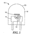
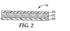
白色光PLEDは、反射ヒートシンク中にUV発光半導体ダイ(チップ)を含みうる。反射ヒートシンクはまた、UV光を部分的に平行にするのに役立ちうる。蛍燐光体含有層の下面にUV光が照射されると、蛍燐光体含有層がUV光の少なくとも一部分を吸収して可視領域の多波長の光を放出し、普通の観察者に実質的に白色に見える光源が提供される。図1は、そのようなPLED10の一構成を示している。PLEDは、導電性ヒートシンク14のウェル中に装着された半導電性LED12を備える。導電性ヒートシンク14はまた、LED12から放出された光の一部分を蛍燐光体−リフレクターアセンブリー16の方向に反射する。アセンブリー16は、PLED10により放出される光を調整すべくレンズ特徴部20を提供するように造形することのできる光透過性ポッティング材料18中に存在しうる。図2に蛍燐光体アセンブリー16をより詳細に示す。蛍燐光体は、バインダーと混合された1種以上の蛍燐光体材料の組合せから層22の形態に形成される。UV励起光は反射するが可視放出光は透過するロングパス(LP)リフレクター24を蛍燐光体層22のトップ表面に適用することができる。可視光は反射するがUV光は透過するショートパス(SP)リフレクター26を層22の下端に適用することができる。
A white light PLED may include a UV light emitting semiconductor die (chip) in a reflective heat sink. A reflective heat sink can also help to partially collimate the UV light. When the lower surface of the phosphor-containing layer is irradiated with UV light, the phosphor-containing layer absorbs at least a part of the UV light and emits multi-wavelength light in the visible region, which is substantially A light source that appears white is provided. FIG. 1 shows one configuration of such a PLED 10. The PLED comprises a
所与の蛍燐光体濃度の蛍燐光体層の最適厚さは、UV光を効率的に吸収すること(光学的に厚い蛍燐光体層が有利である)と可視光を効率的に放出すること(光学的に薄い蛍燐光体層が有利である)と間の妥協点である。さらに、UV光の強度は蛍燐光体層22の下端で最大でありかつ有用な光は蛍燐光体層22の上端から抽出されることになるので、最適厚さを超えて蛍燐光体層22の厚さを増大させると、PLED全体の出力および効率は急速に低下するであろう。 The optimum thickness of the phosphor layer at a given phosphor concentration is effective in absorbing UV light (an optically thick phosphor layer is advantageous) and efficiently emitting visible light. (A thin optical phosphor layer is advantageous). Furthermore, the intensity of the UV light is greatest at the lower end of the phosphor layer 22 and useful light will be extracted from the upper end of the phosphor layer 22, so that the phosphor layer 22 exceeds the optimum thickness. Increasing the thickness of the LED will rapidly decrease the overall power and efficiency of the PLED.
LPリフレクター24およびSPリフレクター26を存在させれば、PLED10の効率を向上させることができる。LPリフレクター24は、蛍燐光体層22により吸収されずそのままでは浪費されるおそれのあるUV光を反射して蛍燐光体層22に戻す。こうすると蛍燐光体層を貫通するUV光の有効経路長が増大されるので、所与の蛍燐光体層厚さの蛍燐光体により吸収されるUV光の量が増大される。かくして、LPリフレクター24を備えていない構成体と比較して最適な蛍燐光体層厚さを減少させることができるので、光発生効率が増大される。
If the
PLEDの他の有意な損失は、蛍燐光体層中における方向無制御状態の光発生が原因であり、これにより、蛍燐光体層22中で発生された可視光の半分がLEDの方向に戻されることになる。ヒートシンクの傾斜壁から反射させることによりこの光の一部分を捕捉することは可能であるが、光の大部分は、散乱されるか、吸収されるか、または品質低下を生じる。この損失は、図示されるようにLED12と蛍燐光体層22との間にSPリフレクター26を配置することにより減少させることができる。
Another significant loss of PLEDs is due to uncontrolled light generation in the phosphor layer, which causes half of the visible light generated in the phosphor layer 22 to return to the LED direction. Will be. While it is possible to capture a portion of this light by reflecting off the inclined walls of the heat sink, most of the light is scattered, absorbed, or degraded. This loss can be reduced by placing an SP reflector 26 between the
PLED構成体の効率をより一層向上させることが有利であろう。PLEDの製造を単純化しかつその製造コストを削減することもまた有利であろう。 It would be advantageous to further improve the efficiency of the PLED structure. It would also be advantageous to simplify the manufacture of PLEDs and reduce their manufacturing costs.
本出願では、ポリマー多層光学フィルムをフィルター素子(すなわち、LPリフレクターおよびSPリフレクター)として利用するPLEDを開示する。多層光学フィルムは、フィルムの厚さ全体にわたり光学的反復ユニットの形態に配置された個別光学層を含み、個別光学層の少なくともいくつかは複屈折性である。隣接光学層は、中入射角〜高入射角のp偏光光の反射率を保持してその漏れを回避する屈折率関係を有する。SPリフレクターは、蛍燐光体により放出された可視光は反射しUV励起光は透過するように位置決めされた反射帯域を生成する厚さ勾配を有する光学的反復ユニットを含む。LPリフレクターは、UV励起光は反射し蛍燐光体により放出された可視光は透過するように位置決めされた反射帯域を生成する異なる厚さ勾配を有する光学的反復ユニットを含む。PLEDの素子として、ポリマー多層光学フィルムはフラットな構成をとりうるか、あるいは少なくとも1層をエンボス加工したり、または球面、放物面、楕円面、もしくは他の形状で湾曲させるように造形したりすることが可能である。 This application discloses PLEDs that utilize polymer multilayer optical films as filter elements (ie, LP reflectors and SP reflectors). Multilayer optical films include individual optical layers arranged in the form of optical repeat units throughout the thickness of the film, at least some of the individual optical layers being birefringent. The adjacent optical layer has a refractive index relationship that maintains the reflectance of the p-polarized light having a medium incident angle to a high incident angle and avoids the leakage thereof. The SP reflector includes an optical repeat unit having a thickness gradient that produces a reflection band positioned to reflect visible light emitted by the phosphor and transmit UV excitation light. The LP reflector includes optical repeat units having different thickness gradients that are positioned to reflect UV excitation light and transmit visible light emitted by the phosphor. As a PLED element, a polymer multilayer optical film can take a flat configuration, or at least one layer can be embossed or shaped to be curved in a spherical, parabolic, elliptical, or other shape. It is possible.
少なくとも1つのポリマー多層光学フィルムと蛍燐光体層とを備えたシート材料を形成することを含むPLEDの製造方法を開示する。いくつかの場合には、2つのポリマー多層光学フィルム間すなわち1つのSPリフレクターと1つのLPリフレクターとの間に蛍燐光体を挟設することができる。他の場合には、1つのポリマー多層光学フィルムだけに蛍燐光体層を適用することができる。ポリマー多層光学フィルムおよび蛍燐光体層は、蛍燐光体−リフレクターアセンブリーを形成する。蛍燐光体−リフレクターアセンブリーの個別部片をシート材料から切り出し、続いて、透明ポッティング材料中に浸漬するかまたは射出成形することにより第1の光学素子を形成し、次に、それを別に製造されたLED素子に結合することができる。シート材料は、必要になるまで便利なロール形態で蛍燐光体−リフレクターアセンブリー部片を保持して保存すべくキャリヤーフィルムを備えうる。PLEDは、蛍燐光体−リフレクターアセンブリーを備えた上側部分にLEDを備えた下側部分を連結するにより作製することができる。また、いくつかの場合には、シート材料をエンボス加工することができる。 Disclosed is a method of manufacturing a PLED comprising forming a sheet material comprising at least one polymer multilayer optical film and a phosphor layer. In some cases, a phosphor can be sandwiched between two polymer multilayer optical films, ie, between one SP reflector and one LP reflector. In other cases, the phosphor layer can be applied to only one polymer multilayer optical film. The polymer multilayer optical film and the phosphor layer form a phosphor-reflector assembly. A separate optical piece of the phosphor-reflector assembly is cut from the sheet material, followed by immersion or injection molding in a transparent potting material to form the first optical element, which is then manufactured separately. The LED element can be coupled. The sheet material may comprise a carrier film to hold and store the phosphor-reflector assembly pieces in a convenient roll form until needed. PLEDs can be made by connecting the lower part with the LED to the upper part with the phosphor-reflector assembly. Also, in some cases, the sheet material can be embossed.
本明細書には、蛍燐光体層により吸収されないすべてのUV励起光が限られた範囲の入射角にわたってLPリフレクターに当たりより効率的に反射されて蛍燐光体層上に戻されるように、曲面LPリフレクターが蛍燐光体層または少なくともその中央光輝部分から離間して配置された、PLEDの実施形態が開示されている。 The present specification describes a curved LP so that all UV excitation light that is not absorbed by the phosphor layer is more efficiently reflected back to the LP reflector over a limited range of incident angles and back onto the phosphor layer. An embodiment of a PLED is disclosed in which the reflector is positioned spaced from the phosphor layer or at least its central bright portion.
本出願には、全内反射を促進すべく多層光学フィルムおよび蛍燐光体層の少なくとも一方に近接したエアギャップを利用するPLEDの実施形態が開示されている。 The present application discloses PLED embodiments that utilize an air gap proximate at least one of a multilayer optical film and a phosphor layer to promote total internal reflection.
本出願には、LPおよび/またはSPリフレクターの性能を向上させるべく非結像コンセントレーター要素の組合せを利用するPLEDの実施形態が開示されている。 The present application discloses PLED embodiments that utilize a combination of non-imaging concentrator elements to improve the performance of LP and / or SP reflectors.
本出願にはまた、LEDからの励起光が蛍燐光体層のフロント主表面に直接反射されるようにLED、LPリフレクター、および蛍燐光体層が配置されたPLEDの実施形態が開示されている。 The application also discloses an embodiment of a PLED in which the LED, LP reflector, and phosphor layer are arranged so that the excitation light from the LED is reflected directly to the front major surface of the phosphor layer. .
開示された実施形態のこれらのおよび他の態様については、以下の詳細な説明から明らかであろう。しかしながら、いかなる場合においても、上記の概要は、特許請求対象を限定するものとみなされるべきものではなく、特許請求対象は、出願手続時に補正される可能性のある添付の特許請求の範囲によってのみ規定される。 These and other aspects of the disclosed embodiments will be apparent from the detailed description below. In no event, however, the above summary should be construed as limiting the claimed subject matter, which is solely subject to the appended claims that may be amended during application processing. It is prescribed.
本明細書全体を通して、添付の図面を参照する。ここで、同じ参照番号は同じ要素を示す。 Throughout this specification, reference is made to the accompanying drawings. Here, the same reference numerals indicate the same elements.
図1〜2に示されるようにLPリフレクター24およびSPリフレクター26の一方または両方を使用することにより系の効率を改善することができるが、ある種のリフレクターでは斜入射角における不十分な分光選択性および不十分な反射率が原因となって改善は制限される。散乱過程に基づくLPミラーまたはLPフィルターは、入射角の関数として比較的一定した性能を達成しうるが、不十分な分光選択性を有する。無機誘電体材料のスタックから構成されるLPミラーおよびSPミラーは、狭範囲の入射角にわたり良好な分光選択性を有しうるが、入射角の増大に伴うスペクトルのブルーシフトおよび中入射角〜高入射角のp偏光光の低反射率(高透過率)の問題を抱えている。蛍燐光体粒子はUV励起光を散乱し、それ自体の光を広範囲の角度にわたり放出するので、従来のLPミラーおよびSPミラーは、蛍燐光体−リフレクターアセンブリー内の光を操作するうえでそれほど効果的でない。
Although the efficiency of the system can be improved by using one or both of the
高分子多層光学フィルム、すなわち、UV波長に制限された反射帯域または可視波長に制限された反射帯域のようなスペクトルの所望の部分において所望の反射率を達成するように厚さおよび屈折率が選択された少なくとも第1および第2のポリマー材料よりなる何十、何百、または何千という交互層を有するフィルムを用いることにより、PLEDの性能を増大させることができる。たとえば、米国特許第5,882,774号明細書(ジョンザ(Jonza)ら)を参照されたい。これらのフィルムにより生成される反射帯域もまた、無機等方性材料のスタックに付随するブルーシフトと同様に入射角によるブルーシフトを受けるが、フィルムに垂直なz軸に関連付けられる隣接層対の屈折率が一致するか、ほぼ一致するか、または計画的に不一致になるように高分子多層光学フィルムを加工することにより、隣接層間の各境界面におけるp偏光光の反射率を入射角と共に徐々に減少させたり、入射角に実質的に依存しないようにしたり、または法線から入射角が離れるにつれて増加させたりすることができる。したがって、そのような高分子多層光学フィルムは、大きい斜入射角度でさえもp偏光光に対して高い反射率レベルを保持しうるので、反射フィルムにより透過されるp偏光光の量は、従来の無機等方性スタックリフレクターと比較して減少する。これらの特性を達成するために、ポリマー材料およびプロセス条件は、各隣接光学層対に対してz軸に沿った(フィルムの厚さに平行な)屈折率差がx軸またはy軸(面内軸)に沿った屈折率差の何分の一以下(0.5倍以下、0.25倍以下、またはさらには0.1倍以下)になるように選択される。他の選択肢として、z軸に沿った屈折率差を面内屈折率差と逆の符号にすることができる。 Polymer multilayer optical film, ie thickness and refractive index selected to achieve the desired reflectivity in the desired part of the spectrum, such as the reflection band limited to UV wavelengths or the reflection band limited to visible wavelengths By using films with dozens, hundreds, or thousands of alternating layers of at least the first and second polymer materials that have been made, the performance of the PLED can be increased. See, for example, US Pat. No. 5,882,774 (Jonza et al.). The reflection bands produced by these films are also subject to a blue shift due to the angle of incidence, similar to the blue shift associated with a stack of inorganic isotropic materials, but the refraction of adjacent layer pairs associated with the z axis perpendicular to the film. By processing the polymer multilayer optical film so that the rates match, nearly match, or systematically match, the reflectance of p-polarized light at each interface between adjacent layers is gradually increased with the incident angle. It can be reduced, made substantially independent of the angle of incidence, or increased as the angle of incidence increases away from the normal. Therefore, since such a polymer multilayer optical film can maintain a high reflectance level for p-polarized light even at a large oblique incident angle, the amount of p-polarized light transmitted by the reflective film is Reduced compared to inorganic isotropic stack reflectors. To achieve these properties, the polymer material and process conditions are such that the refractive index difference along the z-axis (parallel to the film thickness) for each adjacent optical layer pair is x-axis or y-axis (in-plane Selected to be a fraction of the refractive index difference along the axis) (0.5 times or less, 0.25 times or less, or even 0.1 times or less). As another option, the refractive index difference along the z-axis can be opposite in sign to the in-plane refractive index difference.
また、高分子多層光学フィルムを使用すれば、そのようなフィルム(先に言及した屈折率関係を有していても有していなくてもよい)の可撓性および成形性に基づいてさまざまな新しいPLEDの実施形態および構成方法が利用可能になる。たとえば、放物面、球面、または楕円面の一部分のような3次元形状をもたせるべく、エンボス加工、熱成形、または他の公知の手段により、高分子多層光学フィルムを永久変形させることができる。全般については、米国特許出願公開第2002/0154406号明細書(メリル(Merrill)ら)を参照されたい。このほか、さらなる高分子多層フィルムの実施形態については、米国特許第5,540,978号明細書(シュレンク(Schrenk))を参照されたい。以下でさらに説明されるように、剛性で脆い基板上に通常は層ごとに気相堆積される従来の無機等方性スタックとは異なり、高分子多層光学フィルムは、大量のロールの形態で製造可能であり、しかも他のフィルムにラミネートしたりコーティングしたりすることが可能であり、さらにはPLEDのような光学系に容易に組み込めるように小部片にダイカットするかまたは他の方法で細分割することが可能である。高分子多層光学フィルムを細分割する好適な方法は、係属中の米国特許出願第10/268,118号明細書(2002年10月10日出願)に開示されている。 In addition, if a polymer multilayer optical film is used, various films can be used based on the flexibility and moldability of such a film (which may or may not have the refractive index relationship mentioned above). New PLED embodiments and construction methods become available. For example, the polymeric multilayer optical film can be permanently deformed by embossing, thermoforming, or other known means to have a three-dimensional shape, such as a parabolic, spherical, or elliptical portion. See generally US 2002/0154406 (Merrill et al.) For general information. In addition, see US Pat. No. 5,540,978 (Schrenk) for further polymeric multilayer film embodiments. As explained further below, unlike conventional inorganic isotropic stacks, which are typically vapor deposited layer by layer on rigid and brittle substrates, polymeric multilayer optical films are manufactured in the form of large numbers of rolls. Yes, it can be laminated to other films and coated, and even die cut or otherwise subdivided into small pieces for easy integration into optical systems such as PLEDs Is possible. A suitable method for subdividing polymeric multilayer optical films is disclosed in pending US patent application Ser. No. 10 / 268,118 (filed Oct. 10, 2002).
多種多様なポリマー材料が、PLED用の多層光学フィルムに使用するのに好適である。しかしながら、とくに、PLEDが、UV LED励起光源と組み合わされた白色光蛍燐光体エミッターを備える場合、多層光学フィルムは、好ましくは、UV光に暴露されたときに分解に耐える材料で構成された交互ポリマー層を含む。この点に関して、とくに好ましいポリマー対は、ポリエチレンテレフタレート(PET)/co−ポリメチルメタクリレート(co−PMMA)である。ヒンダードアミン光安定化剤(HALS)のような非UV吸収性光安定化剤を組み込むことにより、高分子リフレクターのUV安定性を増大させることもできる。いくつかの場合には、高分子多層光学フィルムは、透明な金属層または金属酸化物層を含みうる。たとえば、PCT国際公開第97/01778号パンフレット(Ouderkirkら)を参照されたい。ロバストなポリマー材料の組合せでさえも許容できないほど劣化させるおそれのあるとりわけ高い強度のUV光が使用される用途では、無機材料を用いて多層スタックを形成することが有益であろう。無機材料層は、等方性であってもよいし、またはPCT国際公開第01/75490号パンフレット(ウェーバー(Weber))に記載されているような形状複屈折性をもたせることによって先に記載したように向上したp偏光反射率を生じる有益な屈折率関係を有するように作製してもよい。しかしながら、ほとんどの場合、多層光学フィルムが無機材料を含まずに実質的に完全に高分子であることが、最も便利でありかつ費用効果的である。 A wide variety of polymeric materials are suitable for use in multilayer optical films for PLEDs. However, especially when the PLED comprises a white light phosphor emitter combined with a UV LED excitation light source, the multilayer optical film is preferably composed of alternating materials composed of materials that resist degradation when exposed to UV light. Includes a polymer layer. In this regard, a particularly preferred polymer pair is polyethylene terephthalate (PET) / co-polymethyl methacrylate (co-PMMA). The incorporation of non-UV absorbing light stabilizers such as hindered amine light stabilizers (HALS) can also increase the UV stability of the polymeric reflector. In some cases, the polymeric multilayer optical film can include a transparent metal layer or metal oxide layer. See, for example, PCT WO 97/01778 (Ouderkirk et al.). In applications where particularly high intensity UV light is used, which may unacceptably degrade even a combination of robust polymeric materials, it may be beneficial to form a multilayer stack with inorganic materials. The inorganic material layer may be isotropic or previously described by having a shape birefringence as described in PCT Publication No. 01/75490 (Weber). It may also be made to have a beneficial refractive index relationship that yields improved p-polarized reflectivity. However, in most cases, it is most convenient and cost effective that the multilayer optical film is substantially completely polymer free of inorganic materials.
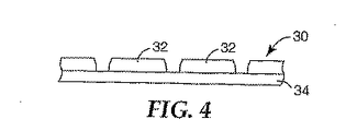
図3は、シート材料のロール30を示している。この材料は、少なくとも1つの高分子多層光学フィルムと、コーティング操作により多層光学フィルムに適用された実質的に均一な蛍燐光体層と、を含む。シート材料は、図2に示されるように、蛍燐光体層が第1および第2の高分子多層光学フィルム間に挟設されるように適用された第2の高分子多層光学フィルムをも含みうる。所望の機械的特性、化学的特性、および/または光学的特性を提供する追加の層およびコーティングをも含みうる。米国特許第6,368,699号明細書(ギルバート(Gilbert)ら)を参照されたい。シート材料30はまた、好ましくはキャリヤーフィルムを含む。シート材料は、ナイフカット、精密ダイカットのような機械的手段により、または先に参照した係属中の‘118出願に記載されているような走査レーザー放射により、キスカットされる。キスカットラインは、原型を保つキャリヤーフィルムを除いてシート材料の個別部片32を規定する。部片32は、図2に示されるものと同様な断面構成をとることが可能であり、またサイズを随意小さくすることが可能である。それらは、図4に示されるような下側のキャリヤーフィルム34によって都合よく支持される。PLEDの製造時(LED光源の構成に依存せずに)、部片32をキャリヤーフィルムから取り出して、ポッティング材料が添加されるかまたはあらかじめ添加された個別の成形型に入れることにより、図1に示されるようなPLEDを形成しうるが、その場合、リフレクター素子には高分子多層光学フィルムが使用される。
FIG. 3 shows a
図5〜7は、凹面形多層光学フィルムLPリフレクターを利用するPLEDの他の構成を示している。LPリフレクターを蛍燐光体から離間させかつ蛍燐光体の方向におよびLED12の方向にそれを内側に湾曲させると、LPリフレクターに当たる励起光の入射角の範囲を狭くするのに役立つので、先に論述したブルーシフト効果により引き起こされるLPリフレクターを貫通するUV光の漏れが減少する。好ましくは、多層光学フィルムは、透明媒体18中に浸漬する前にエンボス加工または他の好適なプロセスによって好適な形状の凹表面の形態に永久変形される。多層光学フィルムは、LPであるかSPであるかにかかわらず、それらのそれぞれの反射帯域内において鏡面リフレクターである。多層光学フィルムからの拡散反射は、典型的には無視できる。
FIGS. 5-7 show other configurations of PLEDs using concave multilayer optical film LP reflectors. The separation of the LP reflector from the phosphor and bending it inward in the direction of the phosphor and in the direction of the
図5では、PLED40は、高分子多層光学フィルムで構成されたオプションのSPリフレクター44上に配設された比較的小面積の蛍燐光体層42を備える。LPリフレクター46は、凹面形状が得られるようにエンボス加工され、蛍燐光体−リフレクターアセンブリーの他の素子(42、44)に隣接して位置決めされている。LED12およびヒートシンク14は、LEDにより放出されたUV励起光を蛍燐光体層42の中央部分の方向に方向付けるように配置される。好ましくは、UV光は、蛍燐光体層42の中心またはその近傍でその最高フルエンスを有する。蛍燐光体層42を初回通過するときに吸収されないUV光は、LPリフレクター46と蛍燐光体層42との間の領域48を貫通した後、LPリフレクター46により反射されて蛍燐光体層の方向に戻される。領域48は、透明ポッティング材料18で構成しうるか、あるいは他の選択肢として他の高分子材料、空気(もしくは他の気体)、またはガラスで構成しうる。LPリフレクター46は、好ましくは、反射されて蛍燐光体の方向に戻されるUV励起光の量を最大化するように造形される。
In FIG. 5, the PLED 40 comprises a relatively small
図6は、蛍燐光体層52、SPリフレクター54、およびLPリフレクター56のサイズが増大されていること以外はPLED40に類似したPLED50を示している。LED12から蛍燐光体層までの所与の距離およびヒートシンク14の同一幾何学形状に対して、より大きいLPリフレクター56は、蛍燐光体層の中央でより高い集束度の光を生成するであろう。蛍燐光体層の中央の発光領域を小さくするほどLPリフレクターの表面に対する蛍燐光体放出光の入射角範囲が小さくなるので、全PLED効率が改善される。先の場合と同じように、領域58は、ポッティング材料18で構成しうるか、あるいは他の高分子材料、空気(もしくは他のガス)、またはガラスで構成しうる。
FIG. 6 shows a PLED 50 that is similar to PLED 40 except that the size of the
図7に示されるPLED60は、このLPリフレクター66が光源の外表面を形成すること以外はPLED50に類似している。領域68は、ポッティング材料18または他の透明媒体で充填しうる。
The PLED 60 shown in FIG. 7 is similar to the PLED 50 except that this
図5〜7の蛍燐光体層は、連続したものであってもよいし、または最も効果的な場所に蛍燐光体を制限するようにパターン化されたものであってもよい。図1および図5〜7の実施形態ならびに蛍燐光体−リフレクターアセンブリーがLEDの上方に離間して配設される他の実施形態では、PLEDを二分割部片として製造することが可能である。すなわち、一方の部片は、ヒートシンクと共にLEDを含有し、他方の部片は、蛍燐光体層および多層リフレクターを含有する。二分割部片を別々に作製し、次に、連結一体化させるかまたは他の方法では固定して一体化させることが可能である。この構成方法は、製造の単純化および全歩留りの増大に役立ちうる。 The phosphor layers of FIGS. 5-7 can be continuous or patterned to limit the phosphor to the most effective locations. In the embodiment of FIGS. 1 and 5-7 and other embodiments in which the phosphor-reflector assembly is spaced apart above the LED, the PLED can be manufactured as a two-part piece. . That is, one piece contains the LED together with the heat sink, and the other piece contains the phosphor layer and the multilayer reflector. The bipartite pieces can be made separately and then linked together or otherwise fixed and integrated. This construction method can help simplify manufacturing and increase overall yield.
図8は、本明細書に記載の他の実施形態に有益に適用しうる概念、すなわち、LEDと蛍燐光体層との間にエアギャップを提供することおよび/または蛍燐光体−リフレクターアセンブリーの1つ以上の要素のすぐ近くにエアギャップを提供することを示している。説明を簡潔にするために、PLEDのいくつかの要素だけを図に示す。エアギャップ70は、多層光学フィルムSPリフレクター74に隣接してLED12と蛍燐光体層72との間に示されている。比較的小さい角度が関与するので、LEDから蛍燐光体層に到達するUV光に及ぼすエアギャップの悪影響はごくわずかである。しかし、エアギャップは、SPリフレクター、蛍燐光体層、およびLPリフレクターの中を伝播する光のような高入射角で伝播する光の全内反射(TIR)を可能にする。図8の実施形態では、SPリフレクターの効率は、リフレクター74の下部表面でTIRを可能にすることにより向上する。他の選択肢として、SPリフレクター74を省略することが可能であり、そして蛍燐光体層72の下側にエアギャップを直接形成することが可能である。また、蛍燐光体層72の上面またはLPリフレクターに隣接してその上部表面もしくは下部表面にエアギャップを形成することも可能である。エアギャップを提供する一方法には、公知のマイクロ構造化フィルムの使用が含まれる。そのようなフィルムは、マイクロ構造化表面に対向して実質的にフラットな表面を有する。マイクロ構造化表面は、単一セットの線形v字形グルーブまたはプリズム、小さな角錐のアレイを規定する複数の交差セットのv字形グルーブ、1セット以上の狭いリッジなどにより特性付けることができる。そのようなフィルムのマイクロ構造化表面を他のフラットフィルムに当接して配置した場合、マイクロ構造化表面の最上部内にエアギャップが形成される。
FIG. 8 illustrates a concept that can be beneficially applied to other embodiments described herein, ie, providing an air gap between an LED and a phosphor layer and / or a phosphor-reflector assembly. Providing an air gap in the immediate vicinity of one or more of the elements. For the sake of brevity, only some elements of the PLED are shown in the figure. An
蛍燐光体によりある波長(励起波長)の光を他の波長(発光波長)に変換する際、熱が生成される。蛍燐光体の近傍にエアギャップが存在すると、蛍燐光体から周囲材料への熱伝達が有意に減少する可能性がある。熱伝達の減少は、他の方法により、たとえば、熱を横方向に除去することのできるガラスまたは透明セラミックの層を蛍燐光体層の近傍に提供することにより、補償することができる。 When light of a certain wavelength (excitation wavelength) is converted into another wavelength (emission wavelength) by the phosphor, heat is generated. The presence of an air gap in the vicinity of the phosphor can significantly reduce heat transfer from the phosphor to the surrounding material. The reduction in heat transfer can be compensated by other methods, for example by providing a glass or transparent ceramic layer in the vicinity of the phosphor layer that can remove heat laterally.
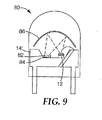
PLEDの効率を改善するさらに他の方法は、蛍燐光体層の下端表面上にUV光の全部を方向付けるのではなく、LEDからのUV光の少なくとも一部分をLPリフレクターにより蛍燐光体層の上端表面(目視表面)に直接反射させるように、LED、蛍燐光体層、およびLPリフレクターを構成する方法である。図9は、そのようなPLED80を示している。ヒートシンク14’は、LED12および蛍燐光体層82を略共面上に装着できるように上記の実施形態に変更が加えられている。SPリフレクターが蛍燐光体層の下側に示されているが、多くの場合、必要ないであろう。この理由は、凹楕円面または類似の形状にエンボス加工されたLPリフレクター86によりUV励起光がLEDから蛍燐光体層82の上部表面(この表面はPLED80の前面の方向を向く)に直接方向付けられることにある。LEDおよび蛍燐光体層は、好ましくは楕円面の焦点に配設される。蛍燐光体層により放出された可視光は、LPリフレクター86を透過してPLED本体の丸みを帯びた前端部により集光され、所望のパターンまたは可視光(好ましくは白色光)を形成する。
Yet another way to improve the efficiency of a PLED is not to direct all of the UV light onto the bottom surface of the phosphor layer, but at least a portion of the UV light from the LED is transmitted by an LP reflector to the top of the phosphor layer. In this method, the LED, the phosphor layer, and the LP reflector are configured to directly reflect on the surface (viewing surface). FIG. 9 shows such a PLED 80. The
励起光を蛍燐光体層のフロント表面に直接方向付けることには、いくつかの利点がある。この場合、励起光が最強である蛍燐光体層の最高光輝部分は、蛍燐光体層の厚さ全体にわたり覆い隠されることなくデバイスの前方に露出される。先に言及した厚さ/明るさのトレードオフを問題にすることなく、UV励起光の実質的にすべてを吸収するように、蛍燐光体層を実質的により厚く作製することができる。銀または機能強化アルミニウムを含む広帯域金属ミラー上に蛍燐光体を装着することができる。 Directing the excitation light directly to the front surface of the phosphor layer has several advantages. In this case, the brightest part of the phosphor layer where the excitation light is strongest is exposed in front of the device without being obscured over the entire thickness of the phosphor layer. The phosphor layer can be made substantially thicker so that it absorbs substantially all of the UV excitation light without questioning the thickness / brightness tradeoff referred to above. The phosphor can be mounted on a broadband metal mirror containing silver or functionally enhanced aluminum.
図10は、LED光が蛍燐光体層のフロント表面に衝突するがLED光の一部がバック表面にも衝突する他のPLEDの実施形態を模式的に示している。この実施形態では、LED12により放出された光の一部は、蛍燐光体層92のバック表面に衝突するが、一部のLED光は、蛍燐光体を貫通することなく、凹面形LPリフレクター96から反射されて蛍燐光体層92のフロント表面にも当たる。次に、蛍燐光体層92により放出された可視光は、目視者または照明対象物の方向にLPリフレクター96を貫通する。LED、蛍燐光体層、およびLPリフレクターはすべて、以上の実施形態に示されるように、透明ポッティング媒体に浸漬または接合することができる。
FIG. 10 schematically illustrates another PLED embodiment in which LED light strikes the front surface of the phosphor layer, but some of the LED light also strikes the back surface. In this embodiment, some of the light emitted by the
図11は、多層光学フィルムの作用を強化するように非結像コンセントレーターが組み合わされて配置された他のPLEDの実施形態を模式的に示している。具体的には、図示されるように、LED12、SPリフレクター104、蛍燐光体層102、およびLPリフレクター106の間に、コンセントレーター要素100a、100b、100cが提供される。コンセントレーター要素は、多層リフレクターに当たる光の角度の広がりを減少させる作用を有するので、図5〜7に関連して先に論述した反射帯域のブルーシフトが低減される。コンセントレーター要素は、滑らかな側壁を有する単純な円錐部分の形態をとりうるか、または側壁は、光の伝播方向に依存して平行化作用もしくは集束作用を強化することが知られているより複雑な曲面形状をとりうる。いずれにせよ、コンセントレーター要素の側壁は反射性であり、2つの端(1つの端は小さく1つの端は大きい)は反射性でない。図11では、LED12は、コンセントレーター100aの小さい端に配設される。コンセントレーター要素100aは、LEDにより放出された広角度範囲の光を集光し、その範囲は、SPリフレクター104が装着されたコンセントレーター要素100aの大きい端にそのような光が伝播するまで低減される。SPリフレクターは、UV励起光を透過させてコンセントレーター要素100bに送り、コンセントレーター要素100bは、そのような光を蛍燐光体層102上に集束させる(それと同時に、光の角度の広がりを増大させる)。蛍燐光体層102により下方に放出された広角度範囲の可視光は、コンセントレーター要素100bによってより狭い角度範囲に変換されてSPリフレクター104に送られ、そこで反射されて蛍燐光体層102の方向に戻される。その間、蛍燐光体層102を貫通して漏れたUV光および蛍燐光体層102により上方に最初に放出された可視光は、広角度の広がりを有するが、コンセントレーター要素100cによってより小角度の広がりに変換されるので、LPリフレクター106は、より良好に、蛍燐光体により放出された可視光を透過するとともに、UV光を反射して蛍燐光体層の方向にもどすであろう。
FIG. 11 schematically illustrates another PLED embodiment in which non-imaging concentrators are placed in combination to enhance the action of the multilayer optical film. Specifically,
できるかぎり多くのLED励起光を捕捉するために、コンセントレーター要素100aの小さい端は、図12に示されるように、LEDの側面により放出された光の少なくとも一部分を捕捉するようにキャビティーを有しうる。
In order to capture as much LED excitation light as possible, the small end of the
本明細書中に開示されている実施形態は、さまざまな蛍燐光体材料を用いて機能する。蛍燐光体材料は、典型的には、300〜450ナノメートルの範囲内の励起波長および可視波長範囲内の発光波長を有する組成をもつ無機物である。狭い発光波長範囲を有する蛍燐光体材料の場合、目視者により感知される所望の色バランスが達成されるように、赤色発光蛍燐光体と緑色発光蛍燐光体と青色発光蛍燐光体との混合物のような蛍燐光体材料の混合物を配合しうる。より高い演色指数を有する蛍燐光体混合物を得るには、より広い発光帯域を有する蛍燐光体材料が有用である。望ましくは、蛍燐光体は、迅速な放射減衰速度を有していなければならない。蛍燐光体ブレンドは、たとえば、エポキシ、接着剤、シリコーン、フルオロカーボン、または高分子マトリックスのようなバインダー中に分散された1〜25ミクロンのサイズ範囲の蛍燐光体粒子を含みうる。このブレンドは、次に、LEDまたはフィルムのような基体に適用することができる。約300〜470nmの範囲内の光をより長い波長に変換する蛍燐光体は、当技術分野で周知である。たとえば、英国エセックスのホルファー・テクノロジー・リミテッド(Phosphor Technology Ltd.,Essex,England)により販売されている蛍燐光体の系列を参照されたい。蛍燐光体は、希土類がドープされたガーネット、シリケート、および他のセラミックスを含む。本明細書中で使用される「蛍燐光体」という用語は、蛍光染料や蛍光顔料などの有機蛍光物質を包含しうる。300〜470nmの放射線下で高い安定性を有する材料が好ましく、とくに無機蛍燐光体が好ましい。 The embodiments disclosed herein function with a variety of phosphor materials. The phosphor material is typically an inorganic material with a composition having an excitation wavelength in the range of 300 to 450 nanometers and an emission wavelength in the visible wavelength range. In the case of a phosphor material having a narrow emission wavelength range, a mixture of a red-emitting phosphor, a green-emitting phosphor and a blue-emitting phosphor so that the desired color balance perceived by the viewer is achieved. A mixture of phosphor materials such as To obtain a phosphor mixture having a higher color rendering index, phosphor materials having a broader emission band are useful. Desirably, the phosphor must have a rapid radiation decay rate. The phosphor blend can include phosphor particles in the size range of 1-25 microns dispersed in a binder such as, for example, epoxy, adhesive, silicone, fluorocarbon, or polymeric matrix. This blend can then be applied to a substrate such as an LED or film. Phosphors that convert light in the range of about 300-470 nm to longer wavelengths are well known in the art. See, for example, the family of phosphors sold by Phosphor Technology Ltd., Essex, England, Essex, UK. Phosphors include garnets, silicates, and other ceramics doped with rare earths. As used herein, the term “phosphor” may include organic fluorescent materials such as fluorescent dyes and fluorescent pigments. A material having high stability under a radiation of 300 to 470 nm is preferable, and an inorganic phosphor is particularly preferable.
特定用語の解説
LED: 可視、紫外、または赤外であるかにかかわらず、またコヒーレントまたはインコヒーレントであるかにかかわらず、光を放出するダイオード。本明細書中で使用されるこの用語は、従来型または超放射型であるかにかかわらず、「LED」として販売されるインコヒーレント(通常は安価)エポキシ封止半導体デバイスを包含する。本明細書中で使用されるこの用語は、半導体レーザーダイオードをも包含する。
可視光: 一般的には約400〜700nmの波長範囲内にある人間の肉眼で知覚可能な光。
光学的反復ユニット(「ORU」): 多層光学フィルムの厚さを横切って反復する少なくとも2層の個別層よりなるスタック。ただし、対応する繰返し層は同一の厚さを有する必要はない。
光学的厚さ: 所与の物体の物理的厚さとその屈折率との積。一般的には、これは波長および偏光の関数である。
反射帯域: 比較的低い反射率の領域により両側が境界付けられた比較的高い反射率のスペクトル領域。
紫外(UV): 波長が約300〜約400nmの範囲内にある光。
白色光: 普通の観察者により「白色」とみなされる外観を生成するように人間の眼の赤色感覚器、緑色感覚器、および青色感覚器を刺激する光。そのような光は、赤色方向に偏移させたり(暖白色光と一般に呼ばれる)、または青色方向に偏移させたり(冷白色光と一般に呼ばれる)することが可能である。そのような光は、100までの演色指数を有しうる。
Glossary of Specific Terms LED: A diode that emits light, whether visible, ultraviolet, or infrared, and whether it is coherent or incoherent. As used herein, this term encompasses incoherent (usually inexpensive) epoxy encapsulated semiconductor devices sold as “LEDs”, whether conventional or superradiant. The term as used herein also includes semiconductor laser diodes.
Visible light: light that is perceptible to the human eye, generally in the wavelength range of about 400-700 nm.
Optical repeat unit ("ORU"): A stack of at least two individual layers that repeat across the thickness of a multilayer optical film. However, the corresponding repeating layers need not have the same thickness.
Optical thickness: The product of the physical thickness of a given object and its refractive index. In general, this is a function of wavelength and polarization.
Reflection band: A relatively high reflectance spectral region bounded on both sides by a relatively low reflectance region.
Ultraviolet (UV): light having a wavelength in the range of about 300 to about 400 nm.
White light: Light that stimulates the red, green, and blue sensory sensations of the human eye to produce an appearance that is considered “white” by a normal observer. Such light can be shifted in the red direction (commonly referred to as warm white light) or can be shifted in the blue direction (commonly referred to as cold white light). Such light can have a color rendering index of up to 100.
さらなる考察
本明細書に記載の干渉リフレクターは、有機材料、無機材料、または有機材料と無機材料との組合せから形成されるリフレクターを包含する。本明細書中で使用される「干渉リフレクター」および「干渉フィルター」という用語は、同義的である。干渉リフレクターは、光の強め合う干渉または弱め合う干渉を引き起こしてリフレクターの反射特性に影響を及ぼす複数の薄層または他の構造体を備えた任意のリフレクターを包含する。干渉リフレクターは多層干渉リフレクターであってもよい。干渉リフレクターは可撓性干渉リフレクターであってもよい。可撓性干渉リフレクターは、高分子材料、非高分子材料、または高分子材料と非高分子材料から形成可能である。高分子材料および非高分子材料を含む例示的なフィルムは、米国特許第6,010,751号明細書および同第6,172,810号明細書ならびに欧州特許出願公開第733,919A2号明細書に開示されている。
Further Considerations Interference reflectors described herein include reflectors formed from organic materials, inorganic materials, or a combination of organic and inorganic materials. As used herein, the terms “interference reflector” and “interference filter” are synonymous. Interference reflectors include any reflector with multiple thin layers or other structures that cause constructive or destructive interference of light and affect the reflective properties of the reflector. The interference reflector may be a multilayer interference reflector. The interference reflector may be a flexible interference reflector. The flexible interference reflector can be formed from a polymeric material, a non-polymeric material, or a polymeric material and a non-polymeric material. Exemplary films comprising polymeric and non-polymeric materials are described in US Pat. Nos. 6,010,751 and 6,172,810 and European Patent Application 733,919 A2. Is disclosed.
本明細書に記載の干渉リフレクターは、可撓性、可塑性、または変形性の材料から形成可能であり、それ自体が可撓性、可塑性、または変形性であってもよい。これらの干渉リフレクターは、従来のLEDと併用可能な半径(すなわち0.5〜5mm)になるように屈撓可能または湾曲可能である。これらの可撓性干渉リフレクターは、屈撓可能または湾曲可能であるとともに、依然として屈撓前の光学的特性を保持しうる。 The interference reflector described herein can be formed from a flexible, plastic, or deformable material, and may itself be flexible, plastic, or deformable. These interference reflectors can bend or bend to a radius that can be used with conventional LEDs (ie 0.5-5 mm). These flexible interference reflectors can bend or bend and still retain the optical properties prior to bending.
コレステリック反射偏光子および特定のブロックコポリマーのような既知の自己集合周期構造体は、本出願の目的では多層干渉リフレクターであるとみなされる。コレステリックミラーは、左旋性および右旋性のキラルピッチ要素の組合せを用いて作製することができる。 Known self-assembled periodic structures, such as cholesteric reflective polarizers and certain block copolymers, are considered multilayer interference reflectors for purposes of this application. Cholesteric mirrors can be made using a combination of levorotatory and dextrorotatory chiral pitch elements.
例示的な実施形態では、青色光の全波長を部分透過するロングパスフィルターは、LEDからの青色光の一部が蛍燐光体を初回通過した後に蛍燐光体層に戻されるように方向付けるべく、薄肉黄色蛍燐光体層と組み合わせて使用することができる。 In an exemplary embodiment, a long pass filter that partially transmits all wavelengths of blue light is directed so that a portion of the blue light from the LED is returned to the phosphor layer after first passing through the phosphor, It can be used in combination with a thin yellow phosphor layer.
UV光の反射を提供することに加えて、多層光学フィルムの機能は、人間の眼の損傷を防止することを含めてLEDパッケージの内部または外部の後続要素の劣化を防止するようにUV光の透過を阻止することであろう。いくつかの実施形態では、LEDから最も離れたUVリフレクター面にUV吸収剤を組み込むことが有利であろう。このUV吸収剤は、多層光学フィルムの内部、面上、または隣接位に存在させうる。 In addition to providing UV light reflection, the function of the multilayer optical film is capable of preventing UV light from deteriorating subsequent elements inside or outside the LED package, including preventing damage to the human eye. It will prevent transmission. In some embodiments, it may be advantageous to incorporate a UV absorber on the UV reflector surface furthest from the LED. The UV absorber may be present in the multilayer optical film, on the surface, or adjacent.
干渉フィルターを製造するためのさまざまな方法が当技術分野で公知であるが、すべてがポリマーである構成体は、いくつかの製造上および費用上の利点を提供しうる。高い光透過率および大きい屈折率差を有する耐熱ポリマーを干渉フィルターに利用すれば、ショートパス(SP)およびロングパス(LP)のフィルターの光学的ニーズを満たすように、薄肉性と高い可撓性とを兼ね備えた環境安定性フィルターを製造することができる。とくに、米国特許第6,531,230号明細書(ウェーバー(Weber)ら)に教示されているような共押出多層干渉フィルターを用いれば、正確な波長選択、さらには大面積、費用効果的な製造が提供できるようになる。大きい屈折率差を有するポリマー対を使用すれば、自立性であるが(すなわち基材を有していないが)依然として加工が容易である非常に薄肉の高反射性ミラーを構成することができる。そのような干渉構造体は、熱成形する時も1mm程度の小さい曲率半径に屈曲させる時も、亀裂を生じたり、飛散したり、他の劣化を生じたりすることはないであろう。 Although various methods for manufacturing interference filters are known in the art, constructs that are all polymers can provide several manufacturing and cost advantages. If heat-resistant polymer with high light transmittance and large refractive index difference is used for interference filter, it is thin and highly flexible to meet the optical needs of short pass (SP) and long pass (LP) filters. It is possible to manufacture an environmental stability filter having both of the above. In particular, co-extruded multilayer interference filters such as taught in US Pat. No. 6,531,230 (Weber et al.) Provide accurate wavelength selection, and even large area, cost effective. Manufacturing can be provided. Using a polymer pair with a large refractive index difference makes it possible to construct a very thin, highly reflective mirror that is self-supporting (ie has no substrate) but is still easy to process. Such an interference structure will not crack, scatter or otherwise degrade when thermoformed or bent to a radius of curvature as small as 1 mm.
すべてがポリマーであるフィルターは、たとえば(以下に記載されているような)半球形ドームなどの種々の3D形状に熱成形することができる。しかしながら、所望の角度性能を得るべく、ドームの全表面にわたり薄層化を適正な量に制御するように注意しなければならない。単純な二次元湾曲を有するフィルターは、3D複合形状フィルターよりも作製が容易である。とくに、薄肉可撓性フィルターであれば、たとえば円柱の一部分のような2D形状に屈曲させることができる。この場合、すべてがポリマーであるフィルターが必要になるわけではない。薄肉高分子基材上の多層無機フィルターは、このようにして造形可能であり、同様にして、厚さ200ミクロン未満のガラス基材上の無機多層も造形可能である。後者の場合には、低応力性の永久造形品を得るべく、ガラス転移点の近傍の温度に加熱しなければならないであろう。 Filters that are all polymeric can be thermoformed into various 3D shapes, such as, for example, a hemispherical dome (as described below). However, care must be taken to control the thinning to the proper amount over the entire surface of the dome to achieve the desired angular performance. A filter having a simple two-dimensional curvature is easier to manufacture than a 3D composite shape filter. In particular, a thin flexible filter can be bent into a 2D shape such as a part of a cylinder. In this case, a filter that is all polymer is not required. A multilayer inorganic filter on a thin polymer substrate can be formed in this manner, and similarly, an inorganic multilayer on a glass substrate having a thickness of less than 200 microns can be formed. In the latter case, it would have to be heated to a temperature in the vicinity of the glass transition point in order to obtain a low-stress permanent shaped article.
ロングパスおよびショートパスのフィルターの最適帯域端は、フィルターを動作させるべく設計されるシステム内のLEDと蛍燐光体の両方の発光スペクトルに依存するであろう。例示的な実施形態では、ショートパスのフィルターに関して言えば、LED発光の実質的にすべてがフィルターを貫通して蛍燐光体を励起し、蛍燐光体発光の実質的にすべてが、LEDまたは吸収される可能性のあるそのベース構造体に進入しないようにフィルターにより反射される。このため、ショートパスを規定する帯域端は、LEDの平均発光波長と蛍燐光体の平均発光波長との間の領域に配置される。例示的な実施形態では、フィルターはLEDと蛍燐光体との間に配置される。しかしながら、フィルターが平面状である場合、典型的なLEDからの発光は、さまざまな角度でフィルターに当たり、ある入射角ではフィルターにより反射されて蛍燐光体に到達しないであろう。ほぼ一定の入射角を保持するようにフィルターが湾曲されていなければ、システム全体の性能を最適化すべく、蛍燐光体の発光曲線とLEDの発光曲線との中点よりも長波長側に設計帯域端を配置することが望まれるであろう。とくに、ほぼゼロ度の入射角でフィルターの方向に方向付けられる蛍燐光体発光はごくわずかである。なぜなら、その囲まれた立体角は非常に小さいからである。 The optimum band edge of the long pass and short pass filters will depend on the emission spectra of both the LED and the phosphor in the system designed to operate the filter. In an exemplary embodiment, when referring to a short-pass filter, substantially all of the LED emission passes through the filter to excite the phosphor, and substantially all of the phosphor emission is LED or absorbed. Reflected by the filter so that it may not enter its possible base structure. For this reason, the band edge that defines the short path is arranged in a region between the average emission wavelength of the LED and the average emission wavelength of the phosphor. In an exemplary embodiment, the filter is disposed between the LED and the phosphor. However, if the filter is planar, the emission from a typical LED will hit the filter at various angles and will be reflected by the filter at a certain angle of incidence and not reach the phosphor. If the filter is not curved to maintain a nearly constant angle of incidence, the design bandwidth is longer than the midpoint between the phosphor emission curve and the LED emission curve to optimize overall system performance. It would be desirable to place the ends. In particular, very little phosphor emission is directed in the direction of the filter at an incident angle of approximately zero degrees. This is because the enclosed solid angle is very small.
他の例示的な実施形態では、システム効率を改善すべくLED励起光がリサイクルされて蛍燐光体に戻されるように、LEDから見て蛍燐光体層の反対側にロングパス反射フィルターを配置する。他の例示的な実施形態では、法線入射よりも高角度でより多くの青色光を透過する分光角度シフトを介して青色LED/黄色蛍燐光体システムの角度性能を最適化すべく、たとえば青色光のような短波光を部分透過するロングパスフィルターを使用することができる。ロングパスリフレクターは、蛍燐光体発光をすべての入射角で効率的に透過するように設計することが可能であり、または角度の関数として所望の出力を達成すべく、変換された励起光を異なる入射角では異なって反射するように設計することが可能である。ロングパスミラーは、いかなる偏光の一次光もしくは励起光に対しても等しい透過を提供するように構成しうるか、または励起光もしくは一次光に対して反射偏光子でありうるか、あるいはその中間の任意の構成体、たとえば部分偏光子でありうる。最終結果として、一次光線の一部分が透過されることになる。ロングパス多層反射偏光子は、本明細書に記載されるように、当技術分野で公知である。いくつかの例は、多層複屈折ポリマー干渉フィルターおよびコレステリック反射偏光子である。 In another exemplary embodiment, a long pass reflective filter is placed on the opposite side of the phosphor layer as viewed from the LED so that the LED excitation light is recycled back to the phosphor to improve system efficiency. In another exemplary embodiment, to optimize the angular performance of a blue LED / yellow phosphor system through a spectral angle shift that transmits more blue light at higher angles than normal incidence, for example, blue light It is possible to use a long pass filter that partially transmits short wave light. Longpass reflectors can be designed to efficiently transmit phosphor emission at all angles of incidence, or differently incident converted excitation light to achieve the desired output as a function of angle. It can be designed to reflect differently at the corners. The long pass mirror can be configured to provide equal transmission for any polarized primary or excitation light, or can be a reflective polarizer for excitation or primary light, or any configuration in between Body, for example a partial polarizer. The net result is that a portion of the primary ray is transmitted. Long pass multilayer reflective polarizers are known in the art, as described herein. Some examples are multilayer birefringent polymer interference filters and cholesteric reflective polarizers.
さらなる例示的な実施形態では、フィルターへのLED放出光の入射角がほぼ一定に保持されるようにLPフィルターを湾曲させる。この実施形態では、蛍燐光体とLEDの両方がLPフィルターの一方の面の方向を向く。高入射角では、LPフィルターは短波光を反射しないであろう。このため、蛍燐光体発光をできるかぎり遮断しないようにしつつ、LPフィルターの長波帯域端を可能なかぎり長波長側に配置することができる。この場合にも、系全体の効率を最適化すべく、帯域端の位置を変化させることができる。 In a further exemplary embodiment, the LP filter is curved so that the angle of incidence of the LED emitted light on the filter is kept substantially constant. In this embodiment, both the phosphor and the LED are oriented toward one side of the LP filter. At high incident angles, the LP filter will not reflect shortwave light. For this reason, the long wave band end of the LP filter can be arranged on the long wavelength side as much as possible while preventing the phosphor emission from being cut off as much as possible. Also in this case, the position of the band edge can be changed in order to optimize the efficiency of the entire system.
「隣接」という用語は、本明細書中では、互いに近くにある2つの物品の相対位置を表すものと定義される。隣接したアイテムは、接触していてもよいし、または隣接したアイテム間に1つ以上の材料を配設して互い離間していてもよい。 The term “adjacent” is defined herein to denote the relative position of two articles that are close to each other. Adjacent items may be in contact or may be spaced apart from each other with one or more materials disposed between adjacent items.
LED励起光は、LED光源が放出しうる任意の光であってよい。LED励起光は、UV光または青色光であってよい。青色光は、菫色光および藍色光を包含する。LEDは、自然発光デバイス、さらには誘導放射発光または超放射発光を用いるデバイス、たとえば、レーザーダイオードおよび垂直キャビティー表面発光レーザーダイオードを包含する。 The LED excitation light may be any light that can be emitted by the LED light source. The LED excitation light may be UV light or blue light. Blue light includes amber light and indigo light. LEDs include spontaneous light emitting devices, as well as devices that use stimulated emission or superradiance emission, such as laser diodes and vertical cavity surface emitting laser diodes.
本明細書に記載の蛍燐光体の層は、連続層であっても不連続層であってもよい。蛍燐光体材料の層は、均一パターンであっても不均一パターンであってもよい。蛍燐光体材料の層は、小さい断面積を有する複数の領域であってもよい。たとえば、平面図において10000マイクロメートル2未満または500〜10000マイクロメートル2の面積を有する複数の「ドット」であってもよい。例示的な実施形態では、複数のドットは、それぞれ、1つ以上の異なる波長の可視光を放出する蛍燐光体から形成可能である。たとえば、赤色発光ドット、青色発光ドット、および緑色発光ドットである。複数の波長の可視光を放出するドットを、所望に応じて任意の均一形態または不均一形態に配置構成しうる。たとえば、蛍燐光体材料の層は、表面または領域に沿って不均一な密度勾配を有する複数のドットであってよい。「ドット」は、任意の規則形状または不規則形状をとることができ、平面図において丸形である必要はない。蛍燐光体材料は、多層光学フィルムの共押出スキン層であってよい。 The phosphor layers described herein may be continuous layers or discontinuous layers. The layer of phosphor material may be a uniform pattern or a non-uniform pattern. The layer of phosphor material may be a plurality of regions having a small cross-sectional area. For example, it may be a plurality of "dots" with an area of 10000 microns 2 or less than 500 to 10,000 micrometers 2 in plan view. In an exemplary embodiment, each of the plurality of dots can be formed from a phosphor that emits one or more different wavelengths of visible light. For example, red light emitting dots, blue light emitting dots, and green light emitting dots. Dots that emit visible light of multiple wavelengths can be arranged and configured in any uniform or non-uniform form as desired. For example, the layer of phosphor material may be a plurality of dots having a non-uniform density gradient along the surface or region. The “dots” can take any regular or irregular shape and need not be round in the plan view. The phosphor material may be a coextruded skin layer of a multilayer optical film.
以下に記載されているように、性能上の利点が得られるように、いくつかの方法で構造化蛍燐光体層を構成することができる。より広いまたはより完全なスペクトル出力が得られるように複数の蛍燐光体タイプを用いる場合、より短波長の蛍燐光体からの光は、他の蛍燐光体に再吸収される可能性がある。各蛍燐光体タイプの独立したドット、線、または独立した領域を含むパターンを用いれば、再吸収量は低減される。吸収されない励起光が反射されて蛍燐光体パターンに戻されるキャビティータイプ構成では、これはとくに効果的であろう。 As described below, the structured phosphor layer can be constructed in several ways to provide performance advantages. When using multiple phosphor types to obtain a broader or more complete spectral output, light from shorter wavelength phosphors may be reabsorbed by other phosphors. Using a pattern that includes independent dots, lines, or independent regions of each phosphor type reduces the amount of reabsorption. This would be particularly effective in a cavity type configuration where unabsorbed excitation light is reflected back into the phosphor pattern.
多層蛍燐光体構造体はまた、吸収を減少させる可能性がある。たとえば、最長波長エミッターが励起光源に最も近い位置にくるようにして各蛍燐光体の層を逐次形成することが有利なこともある。このエミッターにより近い位置で放出された光は、平均して、出力表面の近傍で放出された光よりも多く全蛍燐光体層内で多重散乱を受けるであろう。放出された最短波長が最も散乱を受けやすいので、出力表面に最も近い位置に最短波長蛍燐光体を配置することが有利である。このほか、多層構造体を貫通して伝播するにつれて次第に低下する励起光の強度を補償するように、各層を異なる厚さにすることが有利であろう。放出された蛍燐光体光が後方に散乱されたり順序の先行する蛍燐光体層により再吸収されたりするのを減少させるために、異なる蛍燐光体層間にショートパスフィルターを配置することも有利であろう。 Multilayer phosphor structures can also reduce absorption. For example, it may be advantageous to sequentially form layers of each phosphor so that the longest wavelength emitter is closest to the excitation light source. On average, light emitted closer to this emitter will undergo multiple scattering in the total phosphor layer than light emitted near the output surface. Since the emitted shortest wavelength is most susceptible to scattering, it is advantageous to place the shortest wavelength phosphor at a location closest to the output surface. In addition, it may be advantageous for each layer to have a different thickness so as to compensate for the intensity of the excitation light that gradually decreases as it propagates through the multilayer structure. It is also advantageous to place a short-pass filter between the different phosphor layers in order to reduce the emitted phosphor light being scattered back and reabsorbed by the preceding phosphor layers in sequence. I will.
また、蛍燐光体コーティングでフィルム構造体を形成することにより、ダイオードの個別ユニットにダイシングするのに好適な小さい構造体のアレイの製造が可能である。たとえば、小さいドームまたは半球のアレイを印刷することが可能であり、これらは、それぞれ、PLEDでときどき見られる「ハロー効果」を減少するのに有用である(以下に記載のとおり)。 Also, by forming a film structure with a phosphor coating, it is possible to produce an array of small structures suitable for dicing into individual diode units. For example, it is possible to print an array of small domes or hemispheres, each of which is useful to reduce the “halo effect” sometimes seen with PLEDs (as described below).
非散乱蛍燐光体層を多層光学フィルムと組み合わせることにより、増強された光出力を提供することができる。非散乱蛍燐光体層は、実質的に屈折率の一致したバインダー中もしくは近似的に屈折率の一致したバインダー中の従来の蛍燐光体(たとえば、高屈折率不活性ナノ粒子を有するバインダー)、従来の蛍燐光体組成のナノサイズ粒子(たとえば、粒度が小さく、光散乱が無視できる場合)、または量子ドット蛍燐光体の使用を含みうる。量子ドット蛍燐光体は、電子構造が粒度による影響および制御を受ける程度に十分に小さい粒子の硫化カドミウムのような半導体に基づく光エミッターである。したがって、吸収スペクトルおよび発光スペクトルは、粒度により制御される。量子ドットについては、米国特許第6,501,091号明細書に開示されている。 By combining a non-scattering phosphor layer with a multilayer optical film, an enhanced light output can be provided. The non-scattering phosphor layer is a conventional phosphor in a substantially index-matched binder or in an approximately index-matched binder (eg, a binder with high index inert nanoparticles), It may include the use of nano-sized particles of conventional phosphor composition (eg, where particle size is small and light scattering is negligible), or quantum dot phosphors. Quantum dot phosphors are light emitters based on semiconductors such as cadmium sulfide in particles that are small enough that the electronic structure is influenced and controlled by particle size. Therefore, the absorption spectrum and emission spectrum are controlled by the particle size. Quantum dots are disclosed in US Pat. No. 6,501,091.
蛍燐光体/リフレクターアセンブリーを含む第1の光学素子をLEDベースに装着することが可能であり、かつヒートシンクが、場合により、蛍燐光体層および干渉フィルターを装着することのできる透明ヒートシンクを含みうる実施形態を本明細書中に開示する。透明ヒートシンクは、蛍燐光体層/干渉フィルターとLEDベースとの間に配設されたサファイアの層でありうる。ほとんどのガラスは、ポリマーよりも高い熱伝導率を有し、この機能に同様に有用でありうる。多くの他の結晶性材料の熱伝導率は、ほとんどのガラスよりも高いので、同様にここで使用することができる。サファイア層は、金属ヒートシンクと縁で接触させることができる。 A first optical element including a phosphor / reflector assembly can be mounted to the LED base, and the heat sink optionally includes a transparent heat sink that can be mounted with a phosphor layer and an interference filter. Possible embodiments are disclosed herein. The transparent heat sink can be a layer of sapphire disposed between the phosphor layer / interference filter and the LED base. Most glasses have a higher thermal conductivity than polymers and can be equally useful for this function. Many other crystalline materials have higher thermal conductivities than most glasses and can be used here as well. The sapphire layer can be in contact with the metal heat sink at the edge.
例示的な実施形態では、干渉フィルター(すなわち、高分子干渉フィルター)を蛍燐光体層でコーティングする前に、コーティングの接着性を促進すべくフィルターの表面を処理することができる。最適処理は、フィルターの表面層と蛍燐光体コーティング中の材料(とくに、蛍燐光体粒子を表面上に保持するために使用されるバインダー)の両方に依存する。表面処理は、標準的コロナ放電処理であってもよいし、またはコロナ放電に続くプライミング層であってもよい。プライミング層は、典型的には1ミクロン未満の厚さである。有用なプライミング材料は、PVDC、スルホン化ポリエステルおよびヴィッテル(Vitel)のような他のアモルファスポリエステル、バイネル(Bynel)(デュポン(Dupont))やアドマー(Admer)(ミツイ・ケミカルス(Mitsui Chemicals))のようなマレイン化コポリマー、ならびにエルバックス(Elvax)(デュポン(Dupont))のようなEVAである。蛍燐光体層用のバインダーは、熱可塑性および/または熱成形性であってよく、たとえば、フルオロポリマーまたはシリコン系材料であってよい。 In an exemplary embodiment, before coating an interference filter (ie, a polymer interference filter) with a phosphor layer, the surface of the filter can be treated to promote the adhesion of the coating. Optimal processing depends on both the surface layer of the filter and the material in the phosphor coating, particularly the binder used to hold the phosphor particles on the surface. The surface treatment may be a standard corona discharge treatment or a priming layer following the corona discharge. The priming layer is typically less than 1 micron thick. Useful priming materials include PVDC, sulfonated polyesters and other amorphous polyesters such as Vitel, Bynel (Dupont) and Admer (Mitsui Chemicals). Maleated copolymers, as well as EVA such as Elvax (Dupont). The binder for the phosphor layer may be thermoplastic and / or thermoformable, for example, a fluoropolymer or a silicon-based material.
他のプライミング層としては、たとえば、真空蒸着層、好ましくは、プライミング層を堆積させながらポリマー表面にイオン成分またはプラズマ成分を衝突させるイオンビーム源またはガスプラズマ源のような高エネルギー源からの真空蒸着層が挙げられる。そのようなプライミング層は、典型的にはチタニア層またはシリカ層のような無機材料層である。 Other priming layers include, for example, a vacuum deposition layer, preferably a vacuum deposition from a high energy source such as an ion beam source or a gas plasma source that impinges an ion component or plasma component on the polymer surface while depositing the priming layer. Layer. Such a priming layer is typically an inorganic material layer such as a titania layer or a silica layer.
短波長光を可視光にダウンコンバートするための蛍燐光体の使用に関して多くの注意を与えてきたが、赤外線を可視光にアップコンバートすることも可能である。アップコンバート性蛍燐光体は当技術分野で周知であり、典型的には1個の可視フォトンを生成させるのに2個以上の赤外フォトンを使用する。そのような蛍燐光体を励起するのに必要とされる赤外LEDも明らかにされており、非常に効率的である。ロングパス(LP)フィルターおよびショートパス(SP)フィルターを追加すれば、この過程を用いる可視光源をより効率的に作製することができるが、ただし、この場合、それぞれの機能は、ダウンコンバート性蛍燐光体系と比較して逆になる。SPフィルターは、可視光を透過させつつIR光を蛍燐光体の方向に方向付けるために使用することが可能であり、LPフィルターは、外向きに放出された可視光を目標系またはユーザーの方向に方向付けるために蛍燐光体とLEDとの間で配置することができる。 Although much attention has been given to the use of phosphors to downconvert short wavelength light to visible light, it is also possible to upconvert infrared light to visible light. Upconverting phosphors are well known in the art and typically use two or more infrared photons to generate one visible photon. Infrared LEDs required to excite such phosphors have also been identified and are very efficient. Adding a long pass (LP) filter and a short pass (SP) filter can make a visible light source using this process more efficient, but in this case, each function is down-converting phosphorescence. The opposite is true compared to the system. The SP filter can be used to direct IR light in the direction of the phosphor while transmitting visible light, and the LP filter can direct the outwardly emitted visible light to the target system or user direction. Can be placed between the phosphor and the LED to direct the light.
SPフィルターまたはLPフィルターの寿命は、好ましくは、同一系内のLEDの寿命よりも長いかまたはそれと同等である。高分子干渉フィルターの劣化は、過熱が原因になりうる。過熱により材料のクリープを生じる可能性があり、クリープにより層の厚さ値が変化するので、フィルターにより反射される波長が変化することになる。最悪の場合、過熱によりポリマー材料が融解する可能性があるので、結果として、材料が急速に流動し、波長選択が変化し、さらにはフィルターの不均一性を招く。 The lifetime of the SP filter or LP filter is preferably longer than or equal to the lifetime of the LEDs in the same system. Degradation of the polymer interference filter can be caused by overheating. Overheating can cause the material to creep, and the creep changes the thickness value of the layer, thereby changing the wavelength reflected by the filter. In the worst case, overheating can cause the polymer material to melt, resulting in a rapid flow of the material, changing wavelength selection and even filter non-uniformity.
ポリマー材料の劣化はまた、ポリマー材料に依存して、青色光線、菫色光線、またはUV線のような短波長線(化学線)により引き起こされる可能性もある。劣化速度は、作用光の流束とポリマーの温度の両方に依存する。一般的には、LEDからの距離の増大と共に、温度と流束の両方が減少するであろう。このため、高輝度LED(とくに、UV LED)の場合、設計上可能なかぎり高分子フィルターをLEDから離して配置することが有利である。また、先に記載したような透明ヒートシンク上にポリマーフィルターを配置することにより、フィルターの寿命を改善することもできる。ドーム形フィルターでは、化学線の流束は、LEDからの距離の二乗として減少する。たとえば、曲率中心に位置する単方向性1ワットLEDと共に配置された半径1cmの半球形MOFリフレクターは、1/(2π)ワット/cm2(ドームの表面積=2πcm2)の平均強度を受けるであろう。半径0.5cmでは、ドーム上の平均強度は、その値の4倍すなわち2/πW/cm2になるであろう。LED、蛍燐光体、および多層光学フィルムの系は、光束および温度の制御を考慮に入れて設計することができる。 Degradation of the polymer material can also be caused by short wavelength lines (actinic radiation) such as blue light, amber light, or UV radiation, depending on the polymer material. The rate of degradation depends on both the working light flux and the polymer temperature. In general, both temperature and flux will decrease with increasing distance from the LED. For this reason, in the case of a high-intensity LED (particularly UV LED), it is advantageous to dispose the polymer filter as far away from the LED as possible in design. Moreover, the lifetime of a filter can also be improved by arrange | positioning a polymer filter on the transparent heat sink as described above. In a dome filter, the actinic flux decreases as the square of the distance from the LED. For example, a 1 cm radius hemispherical MOF reflector placed with a unidirectional 1 watt LED located in the center of curvature will receive an average intensity of 1 / (2π) watts / cm 2 (dome surface area = 2πcm 2 ). Let's go. At a radius of 0.5 cm, the average intensity on the dome will be four times that value or 2 / πW / cm 2 . LED, phosphor, and multilayer optical film systems can be designed with light flux and temperature control taken into account.
多層リフレクターに隣接しておよび/または蛍燐光体材料に隣接して、反射偏光子を配設することができる。反射偏光子を用いると、好ましい偏光の光を放出させると同時に、他の偏光の光を反射させることができる。当技術分野で公知の蛍燐光体層および他のフィルム素子を用いると、該反射偏光子により反射された偏光光は偏光解消される可能性があり、そして多層リフレクターと組み合わされた蛍燐光体層または蛍燐光体層からのいずれかの反射により、光はリサイクルされ、固体光デバイス(LED)の偏光光の明るさが増大される。好適な反射偏光子としては、たとえば、コレステリック反射偏光子、1/4波長リターダーを備えたコレステリック反射偏光子、スリーエム・カンパニー(3M Company)から入手可能なDBEF反射偏光子、またはスリーエム・カンパニー(3M Company)から入手可能なDRPF反射偏光子が挙げられる。反射偏光子は、好ましくは、蛍燐光体により放出された波長および角度の実質的な範囲にわたり光を偏光させ、LEDが青色光を放出する場合、LED発光波長範囲を反射することも可能である。 A reflective polarizer can be disposed adjacent to the multilayer reflector and / or adjacent to the phosphor material. When a reflective polarizer is used, light having a preferable polarization can be emitted and light having another polarization can be reflected at the same time. Using phosphor layers and other film elements known in the art, the polarized light reflected by the reflective polarizer can be depolarized and the phosphor layer combined with a multilayer reflector Or any reflection from the phosphor layer will recycle the light and increase the brightness of the polarized light of the solid state light device (LED). Suitable reflective polarizers include, for example, a cholesteric reflective polarizer, a cholesteric reflective polarizer with a quarter-wave retarder, a DBEF reflective polarizer available from 3M Company, or 3M Company (3M DRPF reflective polarizer available from Company). The reflective polarizer preferably polarizes light over a substantial range of wavelengths and angles emitted by the phosphor, and can also reflect the LED emission wavelength range when the LED emits blue light. .
好適な多層リフレクターフィルムは、2つの隣接した層の厚さ方向で屈折率が実質的に一致し、かつ非常に大きいかまたは存在しないブルースター角(p偏光光の反射率がゼロになる角度)を有する複屈折性多層光学フィルムである。これにより、p偏光光に対する反射率が入射角と共に徐々に減少するか、入射角に依存しないか、または法線から入射角が離れるにつれて増加する多層ミラーおよび偏光子を構成することができる。その結果、広い帯域幅にわたり高反射率(ミラーの場合には任意の入射方向の偏光面に対して、偏光子の場合には選択された方向の偏光面に対して)を有する多層フィルムを達成することができる。これらの高分子多層リフレクターは、第1および第2の熱可塑性ポリマーの交互層を含む。交互層は、層に平行に延在する互いに直交するx軸およびy軸ならびにx軸およびy軸に直交するz軸を有する局所座標系を規定し、層の少なくともいくつかは複屈折性である。第1、第2、および第3の互いに直交する軸に沿って偏光された光に対して、第1および第2の層間の屈折率差の絶対値は、それぞれ、Δx、Δy、およびΔzである。第3の軸は、フィルムの平面に直交する。ここで、Δxは約0.05超であり、そしてΔzは約0.05未満である。これらのフィルムについては、たとえば、米国特許第5,882,774号明細書に記載されている。 A suitable multilayer reflector film has a Brewster angle (an angle at which the reflectivity of p-polarized light becomes zero) that has substantially the same refractive index in the thickness direction of two adjacent layers and is very large or absent. It is a birefringent multilayer optical film having Accordingly, it is possible to configure a multilayer mirror and a polarizer in which the reflectivity for p-polarized light gradually decreases with the incident angle, does not depend on the incident angle, or increases as the incident angle moves away from the normal line. The result is a multilayer film with high reflectivity over a wide bandwidth (for the plane of polarization in any incident direction for mirrors and for the plane of polarization selected for polarizers). can do. These polymeric multilayer reflectors include alternating layers of first and second thermoplastic polymers. Alternating layers define a local coordinate system having orthogonal x and y axes extending parallel to the layers and a z axis orthogonal to the x and y axes, and at least some of the layers are birefringent . For light polarized along first, second, and third mutually orthogonal axes, the absolute values of the refractive index differences between the first and second layers are Δx, Δy, and Δz, respectively. is there. The third axis is perpendicular to the plane of the film. Here, Δx is greater than about 0.05 and Δz is less than about 0.05. These films are described, for example, in US Pat. No. 5,882,774.
非平面は、フラットでない表面として定義される。非平面表面は、たとえば、フラットな物品を屈撓させて曲面物品を形成することにより、形成可能である。本発明に有用であるリフレクターは、平面であっても非平面であってもよい。非平面多層リフレクターは、直接的に非平面形状物品にキャストされたものであってもよいし、または平面多層リフレクターから非平面多層リフレクターに熱成形されたものであってもよい。非平面多層リフレクターは凹面形状をとりうる。例示的な実施形態では、非平面多層リフレクターは半球形凹面形状をとりうる。LEDは、非平面多層リフレクターの曲率中心またはその近傍に位置決めされうる。例示的な実施形態では、非平面多層リフレクターは、LEDの方向に開口した半球形凹面形状である。LEDの発光領域の横方向の大きさは、非平面多層リフレクターの最小曲率半径の1/3未満または1/6未満でありうる。 Non-planar is defined as a non-flat surface. A non-planar surface can be formed, for example, by bending a flat article to form a curved article. Reflectors that are useful in the present invention may be planar or non-planar. The non-planar multilayer reflector may be cast directly into a non-planar shaped article, or may be thermoformed from a planar multilayer reflector to a non-planar multilayer reflector. Non-planar multilayer reflectors can have a concave shape. In an exemplary embodiment, the non-planar multilayer reflector can take a hemispherical concave shape. The LED can be positioned at or near the center of curvature of the non-planar multilayer reflector. In an exemplary embodiment, the non-planar multilayer reflector is a hemispherical concave shape that opens in the direction of the LED. The lateral size of the light emitting area of the LED can be less than 1/3 or less than 1/6 of the minimum radius of curvature of the non-planar multilayer reflector.
図13は、PLED構成体の他の実施形態210の概略断面図である。この具体例では、蛍燐光体材料層222はLED212と同一平面上に配設される。蛍燐光体材料層222は、第1の主表面または目視面220と、対向する第2の主表面または非目視面221と、を有する。目視面220とは、干渉リフレクター224および/または光源の出力端の上方でPLED構成体210の方向を向く目視者が見たときの目視面を意味するものとする。
FIG. 13 is a schematic cross-sectional view of another
干渉リフレクター224は、目視者と蛍燐光体材料層222との間に配設可能である。非目視面221は、基材またはリフレクター223上にまたはそれに隣接した形で配設可能である。先に記載したように、この基材またはリフレクター223は、放出光を反射して目視面220の方向に戻すことができる。代替的または追加的に、PLED210を第1の方向に向けることが可能であり、LED212を第1の方向に向けることが可能であり、かつ蛍燐光体材料層222の第1の主表面220を第1の方向に向けることが可能である。
The
LED212から放出された光は、少なくとも部分反射されて蛍燐光体材料層222または蛍燐光体材料層222の第1の主表面もしくは目視面220の方向に戻される。LED放出光の少なくとも一部分は、干渉リフレクター224に当たり、蛍燐光体材料層222上に反射されるが、蛍燐光体材料層222を透過することはない。
The light emitted from the
リフレクター224は、所望に応じて平面状であっても非平面状であってもよい。リフレクター224は、LED放出光を反射して蛍燐光体材料層222の第1の主表面または目視面220の方向に戻すのに好適な湾曲形状として示されている。例示的形状は、LED放出光を反射してLED212を取り囲みうる蛍燐光体材料層222上に戻す回転表面である。いくつかの場合には、回転表面の対称軸は、図に示されるようにLED212を通過しうる。リフレクター224は、LED光を反射し、かつ励起された蛍燐光体層222からの光がPLED構成体210を透過して外に放出されるようにする。いくつかの実施形態では、LED放出光は、最初にロングパスリフレクター224に当たり、LED放出光の少なくとも一部分は、反射されて蛍燐光体材料層222上に戻されるが、最初に蛍燐光体材料層222を透過することはない。
The
図14は、図13に示される実施形態の概略平面図である。第1の主表面または目視面320を有する蛍燐光体材料層322は、LED312を取り囲んだ形で示されている。蛍燐光体材料層322は、先に記載したように構成可能である。LED312と蛍燐光体材料322の第1の主表面または目視面320はいずれも、目視者および/または光源の出力端に向かって同一方向(ページ面から)を向く。
FIG. 14 is a schematic plan view of the embodiment shown in FIG. A
蛍燐光体層322は、内周324および外周325により規定された環形状を有しうる。環形状の蛍燐光体層322の周方向に蛍燐光体材料層322をセグメント化した具体例が示されている。所望に応じて、蛍燐光体材料層322を異なる色の領域にセグメント化しうる。蛍燐光体材料層322に、第1の領域322A、第2の領域322B、第3の領域322C、および第4の領域322D、またはそれよりも多い領域もしくは少ない領域をもたせて、各領域が異なる色を放出するようにすることができる。各領域は、独立して、連続または不連続の蛍燐光体材料層を有しうる。各領域は、独立して、先に記載したように均一または不均一な「ドット」パターンを有しうる。
The
図15は、PLED構成体410の他の実施形態の概略断面図である。この具体例では、蛍燐光体材料層422は、LED412と共に非平面構成体中に配設される。蛍燐光体材料層422は、第1の主表面または目視面420と、対向する第2の主表面または非目視面421と、を有する。この非目視面421は、基材またはリフレクター423上に配設可能である。先に記載したように、この基材またはリフレクター423は、放出光を反射して目視面420の方向に戻すことができる。LED412から放出された光は、少なくとも部分反射されて蛍燐光体材料層422の目視面420の方向に戻されるが、最初に蛍燐光体材料層422を透過することはない。
FIG. 15 is a schematic cross-sectional view of another embodiment of a PLED
リフレクター424は、所望に応じて平面状であっても非平面状であってもよい。リフレクター424は、LED放出光を反射して蛍燐光体材料層422の第1の主表面または目視面420の方向に戻すのに好適な湾曲形状として示されている。例示的形状は、LED放出光を反射してLED412を取り囲みうる蛍燐光体材料層422上に戻す凹面形状である。リフレクター424は、LED光を反射し、かつ励起された蛍燐光体層422からの光がPLED構成体410を透過して外に放出されるようにする。
The
本明細書に記載の蛍燐光体ルミネセンスの測定は、積分球(商品名OL IS−670−LED,オプトロニック・ラボラトリーズ(Optronic Laboratories)製)および高精度LEDホルダー(商品名OL 700−80−20,オプトロニック・ラボラトリーズ(Optronic Laboratories)製)を備えた分光放射計(商品名OL 770−LED,米国フロリダ州オーランドのオプトロニック・ラボラトリーズ・インコーポレーテッド(Optronic Laboratories,Inc.,Orlando,Florida,USA)製)を用いて行った。入力ポートから積分球に入る全放射エネルギー(ワット毎ナノメートルの単位)を報告すべく、分光放射計を校正する。カスタムパンチを用いて蛍燐光体コーテッドサンプルから直径1インチのディスクを作製された。このディスクは、高精度LEDホルダーに取り付けるように作製されたカスタムフィルムアダプターに嵌入する。カスタムアダプターは、パッケージ化LEDのベースから上方に約1インチの位置にフィルムサンプルを保持する。LEDをホルダー中に取り付け、蛍燐光体コーティングを有するフィルムをアダプター中に配置し、アダプターを発光ダイオードマウントに固定し、次に、ダイオードマウントアセンブリーを積分球の入口孔に挿入することにより、測定を行った。所要により、校正された中性濃度フィルターを用いて分光放射計の検出器に到達する光レベルを調整した。 The phosphor luminescence measurements described herein were measured using an integrating sphere (trade name OL IS-670-LED, manufactured by Optronic Laboratories) and a high-precision LED holder (trade name OL 700-80-). 20, Spectroradiometer (trade name OL 770-LED, manufactured by Optronic Laboratories), Optronic Laboratories, Inc., Orlando, Florida, United States, Florida, USA )). Calibrate the spectroradiometer to report the total radiant energy (in watts per nanometer) entering the integrating sphere from the input port. A 1 inch diameter disc was made from a phosphor coated sample using a custom punch. This disc fits into a custom film adapter made to attach to a high precision LED holder. The custom adapter holds the film sample approximately 1 inch above the base of the packaged LED. Measurement by mounting the LED in the holder, placing the film with the phosphor coating in the adapter, fixing the adapter to the light emitting diode mount, and then inserting the diode mount assembly into the inlet hole of the integrating sphere Went. If necessary, the light level reaching the detector of the spectroradiometer was adjusted using a calibrated neutral density filter.
別段の記載がないかぎり、以下の実施例で使用した多層光学フィルムは、法線入射において両方の偏光状態を等しく反射するものであった(すなわち、各個別光学層は、直交する面内軸に沿って名目上等しい屈折率を有していた)。 Unless otherwise stated, the multilayer optical films used in the following examples were those that reflected both polarization states equally at normal incidence (ie, each individual optical layer had an orthogonal in-plane axis. Along with a nominally equal refractive index).
蛍燐光体層の厚さが与えられている以下の実施例のいずれについても、厚さは、蛍燐光体層および基材フィルムの合計厚さから基材フィルムの厚さを引くことにより決定したものである。厚さは、ダイヤルゲージスタンド(カタログ番号52−580−020,ファウラー(Fowler)製)に取り付けられたフラット接点(カタログ番号52−525−035,ファウラー(Fowler)製)を有するダイヤルインジケーター(カタログ番号52−520−140,米国マサチューセッツ州ニュートンのフレッド・ヴィ・ファウラー・カンパニー・インコーポレーテッド(Fred V.Fowler Co.,Inc.,of Newton,Massachusetts,USA))を用いて測定した。基材フィルムの厚さは、基材フィルム上のランダムな位置における3つの測定値を平均したものである。蛍燐光体層および基材フィルムの厚さは、蛍燐光体層上のランダムな位置における6つの測定値を平均したものである。 For any of the following examples where the thickness of the phosphor layer is given, the thickness was determined by subtracting the thickness of the substrate film from the total thickness of the phosphor layer and the substrate film. Is. The thickness is a dial indicator (catalog number) having a flat contact (catalog number 52-525-035, fowler) attached to a dial gauge stand (catalog number 52-580-020, made by Fowler). 52-520-140, Fred V. Fowler Company, Inc., Newton, Mass. (Fred V. Fowler Co., Inc., of Newton, Massachusetts, USA). The thickness of the base film is an average of three measured values at random positions on the base film. The thickness of the phosphor layer and the substrate film is an average of six measurements at random locations on the phosphor layer.
実施例1
セリウムをドープしたイットリウムアルミニウムガーネット(YAG:Ce)蛍燐光体のコーティングを、次の手順により、単一層透明ポリ(エチレンテレフタレート)(PET)フィルム上に作製した。
Example 1
A coating of cerium doped yttrium aluminum garnet (YAG: Ce) phosphor was made on a single layer transparent poly (ethylene terephthalate) (PET) film by the following procedure.
12.00グラムのフルオロポリマー樹脂(商品名「ホスファー・インク・パートA:レジン・ソルージョン(Phosphor Ink Part A:Resin Solution)」,製品番号:1INR001、rev:AA,バッチ番号:KY4−035,米国アリゾナ州チャンドラーのジュレル・カンパニー(Durel Company of Chandler,Arizona,USA)製)を40ミリリットルのガラスジャーに入れた。15.02グラムのYAG:Ce蛍燐光体(商品名QMK58/F−U1,ロット#13235,英国スティーベネッジのホスファー・テクノロジー・リミテッド(Phosphor Technology,Ltd.of Stevenage,England)製)を計量して秤量ディッシュに入れた。最初に蛍燐光体の半分を樹脂に添加し、次にステンレス鋼スパチュラを用いて手で混合し、その後、残りの半分を添加して手で混合することにより、蛍燐光体を樹脂と混合した。混合物が平滑テクスチャーおよび均一な外観をもつようになるまで、蛍燐光体と樹脂を手で混合した。得られた蛍燐光体ペーストの入っているジャーを蓋でカバーし、ボトルローラー上に約30分間配置した。 12.00 grams of fluoropolymer resin (trade name “Phosphor Ink Part A: Resin Solution”, product number: 1 INR001, rev: AA, batch number: KY4-035, USA The Jurell Company of Chandler, Arizona (Durele Company of Chandler, Arizona, USA) was placed in a 40 milliliter glass jar. Weigh and weigh 15.02 grams of YAG: Ce phosphor (product name QMK58 / F-U1, Lot # 13235, Phosphor Technology, Ltd. of Stevenage, England, UK) I put it in the dish. First, half of the phosphor was added to the resin, then mixed by hand with a stainless steel spatula, and then the other half was added and mixed by hand to mix the phosphor with the resin. . The phosphor and resin were mixed by hand until the mixture had a smooth texture and uniform appearance. The resulting jar containing the phosphor paste was covered with a lid and placed on a bottle roller for about 30 minutes.
ミネソタ州セントポールのスリーエム・カンパニー(3M Company(St.Paul,MN))製の幅6インチ×長さ10インチ(250マイクロメートル)×厚さ1.5ミル(40マイクロメートル)の単層透明PETフィルムシートを、クリーンなフラット表面上に配置した。メタノールで湿潤させたリントフリー綿布でPETフィルムの両側の表面を払拭した。蛍燐光体ペーストの入っているジャーをボトルローラーから取り出し、約5グラムのペーストをPETフィルム上に小さい溜りの状態に配置した。5ミル(130マイクロメートル)のギャップの正方形マルチクリアランスアプリケーター(商品名PAR−5357,米国メリーランド州コロンビアのビーワイケー・ガードナー・ユーエスエイ(BYK−Gardner USA of Columbia,Maryland,USA)製)を用いて、蛍燐光体ペーストをコーティングの状態に手作業で引き延ばした。重力対流式オーブン(商品名モデル1350G(Model 1350G),米国ペンシルバニア州ウェストチェスターのヴィダブリューアール・インターナショナル・インコーポレーテッド(VWR International, Inc.,of West Chester,Pennsylvania,USA)製)内で約130℃の温度で湿潤フィルムを30分間硬化させた。硬化後、蛍燐光体/樹脂コーティングの厚さは1.6ミル(40マイクロメートル)であった。 Single-layer transparent 6 inches wide x 10 inches long (250 micrometers) x 1.5 mils thick (40 micrometers) manufactured by 3M Company (St. Paul, MN), St. Paul, Minnesota A PET film sheet was placed on a clean flat surface. The surfaces on both sides of the PET film were wiped with a lint-free cotton cloth moistened with methanol. The jar containing the phosphor paste was removed from the bottle roller and about 5 grams of paste was placed in a small pool on the PET film. Using a 5 mil (130 micrometer) gap square multi-clearance applicator (trade name PAR-5357, manufactured by BYK-Gardner USA of Columbia, Maryland, USA) The phosphor paste was manually stretched into the coating state. About 130 ° C. in a gravity convection oven (trade name model 1350G (Model 1350G), manufactured by VWR International, Inc., West West, Pennsylvania, USA), Westchester, PA, USA The wet film was cured at a temperature of 30 minutes. After curing, the phosphor / resin coating thickness was 1.6 mils (40 micrometers).
YAG:Ceコーテッドフィルムの直径1インチ(25mm)のディスクを作製し、先に記載した分光放射計中に取り付けた。蛍燐光体コーテッド面が積分球の方向を向くように、ディスクの向きを変えた。約463nmのピーク波長の青色LED(製品番号25−365,オハイオ州ストューベンヴィルのホスフェルト・エレクトロニックス・インコーポレーテッド(Hosfelt Electronics,Inc.,Steubenville,OH)製)を用いて蛍燐光体を励起した。青色光のフラット出口面を提供するようにパッケージの上端のドーム形レンズを機械加工することにより、青色LED用の標準的5mmパッケージを改造した。パッケージの約0.18インチ(4.6mm)をパッケージの上端から除去した。定電流電源により20ミリアンペアおよび3.46ボルトでLEDに電力供給した。分光放射計を用いて記録した蛍燐光体層の発光スペクトルを、「実施例1」と記された曲線として図16に示す。分光放射計に付属するソフトウェアを用いて、積分球中に放出された全光束を算出したところ、0.068ルーメンであった。 A 1 inch (25 mm) diameter disc of YAG: Ce coated film was made and mounted in the spectroradiometer described above. The orientation of the disc was changed so that the phosphor-coated surface was oriented toward the integrating sphere. Exciting phosphors using a blue LED with a peak wavelength of about 463 nm (product number 25-365, manufactured by Hosvelt Electronics, Inc., Stevenville, OH), Stuvenville, Ohio did. A standard 5 mm package for blue LEDs was modified by machining the top dome-shaped lens of the package to provide a flat exit surface for blue light. Approximately 0.18 inch (4.6 mm) of the package was removed from the top of the package. The LED was powered by a constant current power supply at 20 milliamps and 3.46 volts. The emission spectrum of the phosphor layer recorded using a spectroradiometer is shown in FIG. 16 as the curve labeled “Example 1”. Using the software attached to the spectroradiometer, the total luminous flux emitted into the integrating sphere was calculated to be 0.068 lumen.
実施例2
PETおよびco−PMMAの交互層を有し、かつ約600nm〜約1070nmの法線入射反射帯域(最大値の半分の位置で測定)を有する多層光学フィルム(MOF)(米国特許第6,531,230号明細書に従って作製)の部片を、実施例1の蛍燐光体コーテッドPETフィルムと実施例1の青色LED(20ミリアンペアで動作)と間のフィルムアダプター中に配置した。スペクトルを記録し、「実施例2」と記された曲線として図16に示す。分光放射計に付属するソフトウェアを用いて、積分球中に放出された全光束を算出したところ、0.118ルーメンであった。これは73%の光度増加を表す。
Example 2
A multilayer optical film (MOF) (US Pat. No. 6,531, with alternating layers of PET and co-PMMA and having a normal incidence reflection band (measured at half the maximum value) of about 600 nm to about 1070 nm No. 230) was placed in a film adapter between the phosphor coated PET film of Example 1 and the blue LED of Example 1 (operating at 20 milliamps). The spectrum was recorded and shown in FIG. 16 as the curve labeled “Example 2”. Using the software attached to the spectroradiometer, the total luminous flux emitted into the integrating sphere was calculated to be 0.118 lumen. This represents a 73% increase in luminous intensity.
実施例3
硫化亜鉛(ZnS)蛍燐光体のコーティングを、次の手順により、ポリ(エチレンテレフタレート)(PET)フィルム上に作製した。
Example 3
A coating of zinc sulfide (ZnS) phosphor was made on a poly (ethylene terephthalate) (PET) film by the following procedure.
20.04グラムのフルオロポリマー樹脂(商品名「ホスファー・インク・パートA:レジン・ソルージョン(Phosphor Ink Part A:Resin Solution)」,製品番号:1INR001、rev:AA,バッチ番号:KY4−035,米国アリゾナ州チャンドラーのジュレル・カンパニー(Durel Company of Chandler,Arizona,USA)製)を2オンスのガラスジャーに入れた。20.06グラムのZnS蛍燐光体(商品名GL29A/N−C1,ロット番号11382,英国スティーベネッジのホスファー・テクノロジー・リミテッド(Phosphor Technology,Ltd.of Stevenage,England)製)を計量して秤量ディッシュに入れた。最初に蛍燐光体の半分を樹脂に添加し、次にステンレス鋼スパチュラを用いて手で混合し、その後、残りの半分を添加して手で混合することにより、蛍燐光体を樹脂中に混合した。混合物が平滑なテクスチャーおよび均一な外観をもつようになるまで、蛍燐光体と樹脂を手で混合した。得られた蛍燐光体ペーストの入っているジャーを蓋でカバーし、ボトルローラー上に約24時間配置した。 20.04 grams of fluoropolymer resin (trade name “Phosphor Ink Part A: Resin Solution”, product number: 1 INR001, rev: AA, batch number: KY4-035, USA A Juel Company of Chandler, Arizona (Durele Company of Chandler, Arizona, USA) was placed in a 2 ounce glass jar. Weigh 20.06 grams of ZnS phosphor (trade name GL29A / N-C1, lot number 11382, manufactured by Phosphor Technology, Ltd. of Stevenage, England, UK) I put it in. First add half of the phosphor to the resin, then mix by hand with a stainless steel spatula, then add the other half and mix by hand to mix the phosphor into the resin did. The phosphor and resin were mixed by hand until the mixture had a smooth texture and uniform appearance. The resulting jar containing the phosphor paste was covered with a lid and placed on a bottle roller for about 24 hours.
ミネソタ州セントポールのスリーエム・カンパニー(3M Company(St.Paul,MN))製の幅6インチ×長さ10インチ×厚さ1.5ミル(45マイクロメートル)の透明PETフィルムシートを、クリーンなフラット表面上に配置した。メタノールで湿潤させたリントフリー綿布でPETフィルムの両側の表面を払拭した。蛍燐光体ペーストの入っているジャーをボトルローラーから取り出し、約3グラムのペーストをPETフィルム上に配置した。2ミル(50マイクロメートル)のギャップの正方形マルチクリアランスアプリケーター(商品名PAR−5353,米国メリーランド州コロンビアのビーワイケー・ガードナー・ユーエスエイ(BYK−Gardner USA of Columbia,Maryland,USA)製)を用いて、蛍燐光体ペーストをコーティングの状態に手作業で引き延ばした。重力対流式オーブン(商品名モデル1350G(Model 1350G),米国ペンシルバニア州ウェストチェスターのヴィダブリューアール・インターナショナル・インコーポレーテッド(VWR International, Inc.,of West Chester,Pennsylvania,USA)製)内で約130℃の温度で湿潤フィルムを30分間硬化させた。硬化後、蛍燐光体/樹脂コーティングの厚さは0.7ミル(18マイクロメートル)であった。 A clear PET film sheet 6 cm wide x 10 inches long x 1.5 mils thick (45 micrometers) manufactured by 3M Company, St. Paul, Minn. Placed on a flat surface. The surfaces on both sides of the PET film were wiped with a lint-free cotton cloth moistened with methanol. The jar containing the phosphor paste was removed from the bottle roller and approximately 3 grams of paste was placed on the PET film. Using a 2 mil (50 micrometer) gap square multi-clearance applicator (trade name PAR-5353, manufactured by BYK-Gardner USA of Columbia, Maryland, USA) The phosphor paste was manually stretched into the coating state. About 130 ° C. in a gravity convection oven (trade name model 1350G (Model 1350G), manufactured by VWR International, Inc., West West, Pennsylvania, USA), Westchester, PA, USA The wet film was cured at a temperature of 30 minutes. After curing, the phosphor / resin coating thickness was 0.7 mil (18 micrometers).
ZnSコーテッドフィルムの直径1インチ(25mm)のディスクを作製し、先に記載した分光放射計中に取り付けた。蛍燐光体コーテッド面が積分球の方向を向くように、ディスクの向きを変えた。約395nmのピーク波長のUV LED(製品番号25−495,オハイオ州ストューベンヴィルのホスフェルト・エレクトロニックス・インコーポレーテッド(Hosfelt Electronics,Inc of Steubenville,OH)製)を用いて蛍燐光体蛍光を発生させた。UV光のフラット出口面を提供するようにパッケージのドーム形上端を機械加工で除去することにより、UV LED用の標準的5mmパッケージを改造した。パッケージの約0.18インチ(5mm)をパッケージの上端から除去した。定電流電源により20ミリアンペアおよび3.7ボルトでLEDに電力供給した。分光放射計を用いて記録した蛍燐光体層の発光スペクトルを、「実施例3」と記された曲線として図17に示す。分光放射計に付属するソフトウェアを用いて、積分球中に放出された全光束を算出したところ、0.052ルーメンであった。 A 1 inch (25 mm) diameter disk of ZnS coated film was made and mounted in the spectroradiometer described above. The orientation of the disc was changed so that the phosphor-coated surface was oriented toward the integrating sphere. Phosphor fluorescence is generated using a UV LED with a peak wavelength of about 395 nm (product number 25-495, manufactured by Hosvelt Electronics, Inc. of Stephenville, OH). I let you. A standard 5 mm package for UV LEDs was modified by machining away the dome-shaped top end of the package to provide a flat exit surface for UV light. About 0.18 inch (5 mm) of the package was removed from the top of the package. The LED was powered by a constant current power supply at 20 milliamps and 3.7 volts. The emission spectrum of the phosphor layer recorded using a spectroradiometer is shown in FIG. 17 as the curve labeled “Example 3”. Using the software attached to the spectroradiometer, the total luminous flux emitted into the integrating sphere was calculated to be 0.052 lumen.
実施例4
PETおよびco−PMMAの交互層を有し、かつ約320nm〜約490nmの法線入射反射帯域(最大値の半分の位置で測定)を有する多層光学フィルム(MOF)(米国特許第6,531,230号明細書に従って作製)の部片を、実施例3の蛍燐光体層の上のフィルムアダプター中に配置し、実施例3のUV LED(20ミリアンペアで動作)を励起光源として使用した。スペクトルを記録し、「実施例4」と記された曲線として図17に示す。分光放射計に付属するソフトウェアを用いて、積分球中に放出された全光束を算出したところ、0.062ルーメンであった。これは、実施例3と比較したとき約19%の光度増加を表す。
Example 4
A multilayer optical film (MOF) having alternating layers of PET and co-PMMA and having a normal incidence reflection band (measured at half the maximum value) of about 320 nm to about 490 nm (US Pat. No. 6,531, No. 230) was placed in a film adapter on the phosphor layer of Example 3 and the UV LED of Example 3 (operating at 20 milliamps) was used as the excitation light source. The spectrum was recorded and shown in FIG. 17 as the curve labeled “Example 4”. Using the software attached to the spectroradiometer, the total luminous flux emitted into the integrating sphere was calculated to be 0.062 lumen. This represents an increase in luminous intensity of about 19% when compared to Example 3.
実施例5
多層光学フィルム(MOF)の2つの部片をラミネートすることにより、広帯域可視リフレクターを作製した。PETおよびco−PMMAの交互層を有し、かつ約490nm〜約610nmの法線入射反射帯域(最大値の半分の位置で測定)を有するMOF(ミネソタ州セントポールのスリーエム・カンパニー(3M Company of St.Paul,MN)製)の層を、PETおよびco−PMMAの交互層を有し、かつ約590nm〜約710nmの法線入射反射帯域(最大値の半分の位置で測定)を有するMOF(ミネソタ州セントポールのスリーエム・カンパニー(3M Company of St.Paul,MN)製)の層に、光学的透明接着剤によりラミネートした。実施例3の蛍燐光体コーテッドPETフィルムと実施例3のUV LED(20ミリアンペアで動作)との間のフィルムアダプター中にラミネートを配置した。PETおよびco−PMMAの交互層を有し、かつ約320nm〜約490nmの法線入射反射帯域(最大値の半分の位置で測定)を有する多層光学フィルム(MOF)(ミネソタ州セントポールのスリーエム・カンパニー(3M Company of St.Paul,MN)製)の部片を、蛍燐光体層の上のフィルムアダプター中に配置し、LED側の可視ミラーと他方の側のUV/青色ミラーとの間に挟設された蛍燐光体層を有するキャビティーを形成するようにした。スペクトルを記録し、「実施例5」と記された曲線として図17に示す。分光放射計に付属するソフトウェアを用いて、積分球中に放出された全光束を算出したところ、0.106ルーメンであった。これは、実施例3と比較したとき約104%の光度増加を表す。
Example 5
A broadband visible reflector was made by laminating two pieces of multilayer optical film (MOF). MOF (3M Company of St. Paul, Minn.) With alternating layers of PET and co-PMMA and having a normal incidence reflection band (measured at half the maximum) of about 490 nm to about 610 nm (M. St. Paul, MN)) having a normal incidence reflection band (measured at half the maximum value) of about 590 nm to about 710 nm with alternating layers of PET and co-PMMA and A layer of 3M Company of St. Paul, Minn. (3M Company of St. Paul, MN) was laminated with an optically clear adhesive. The laminate was placed in a film adapter between the phosphor coated PET film of Example 3 and the UV LED of Example 3 (operating at 20 milliamps). Multi-layer optical film (MOF) with alternating layers of PET and co-PMMA and having a normal incidence reflection band (measured at half maximum) of about 320 nm to about 490 nm (Three M., St. Paul, Minn.) A piece of the company (manufactured by 3M Company of St. Paul, MN) is placed in a film adapter on the phosphor layer, between the visible mirror on the LED side and the UV / blue mirror on the other side. A cavity having a sandwiched phosphor layer was formed. The spectrum was recorded and shown in FIG. 17 as the curve labeled “Example 5”. Using the software attached to the spectroradiometer, the total luminous flux emitted into the integrating sphere was calculated to be 0.106 lumen. This represents an increase in luminous intensity of about 104% when compared to Example 3.
実施例6
硫化亜鉛(ZnS)蛍燐光体のコーティングを、次の手順により、ポリ(エチレンテレフタレート)(PET)フィルム上に作製した。
Example 6
A coating of zinc sulfide (ZnS) phosphor was made on a poly (ethylene terephthalate) (PET) film by the following procedure.
実施例3に記載した蛍燐光体ペーストを、幅6インチ×長さ10インチ×厚さ1.5ミル(40マイクロメートル)の透明PETフィルムシート上にコーティングした。PETをクリーンなフラット表面上に配置した。メタノールで湿潤させたリントフリー綿布でPETフィルムの両側の表面を払拭した。約3グラムのペーストをPETフィルム上に配置した。4ミル(100マイクロメートル)のギャップの正方形マルチクリアランスアプリケーター(商品名PAR−5353,米国メリーランド州コロンビアのビーワイケー・ガードナー・ユーエスエイ(BYK−Gardner USA of Columbia,Maryland,USA)製)を用いて、蛍燐光体ペーストをコーティングの状態に手作業で引き延ばした。重力対流式オーブン(商品名モデル1350G(Model 1350G),米国ペンシルバニア州ウェストチェスターのヴィダブリューアール・インターナショナル・インコーポレーテッド(VWR International, Inc.,of West Chester,Pennsylvania,USA)製)内で約130℃の温度で湿潤フィルムを30分間硬化させた。硬化後、蛍燐光体/樹脂コーティングの厚さは1.3ミル(33マイクロメートル)であった。 The phosphor paste described in Example 3 was coated on a transparent PET film sheet 6 inches wide x 10 inches long x 1.5 mils thick (40 micrometers). PET was placed on a clean flat surface. The surfaces on both sides of the PET film were wiped with a lint-free cotton cloth moistened with methanol. About 3 grams of paste was placed on the PET film. Using a 4 mil (100 micrometer) gap square multi-clearance applicator (trade name PAR-5353, manufactured by BYK-Gardner USA of Columbia, Maryland, USA) The phosphor paste was manually stretched into the coating state. About 130 ° C. in a gravity convection oven (trade name model 1350G (Model 1350G), manufactured by VWR International, Inc., West West, Pennsylvania, USA), Westchester, PA, USA The wet film was cured at a temperature of 30 minutes. After curing, the phosphor / resin coating thickness was 1.3 mil (33 micrometers).
ZnSコーテッドフィルムの直径1インチ(25.4mm)のディスクを作製し、先に記載した分光放射計中に取り付けた。蛍燐光体コーテッド面が積分球の方向を向くように、ディスクの向きを変えた。約395nmのピーク波長のUV LED(製品番号25−495,オハイオ州ストューベンヴィルのホスフェルト・エレクトロニックス・インコーポレーテッド(Hosfelt Electronics,Inc of Steubenville,OH)製)を用いて蛍燐光体を励起した。UV光のフラット出口面を提供するようにパッケージのドーム形上端を機械加工で除去することにより、UV LED用の標準的5mmパッケージを改造した。パッケージの約0.18インチ(5mm)をパッケージの上端から除去した。定電流電源により20ミリアンペアおよび3.7ボルトでLEDに電力供給した。分光放射計を用いて記録した蛍燐光体層の発光スペクトルを、「実施例6」と記された曲線として図18に示す。分光放射計に付属するソフトウェアを用いて、積分球中に放出された全光束を算出したところ、0.066ルーメンであった。 A 1 inch (25.4 mm) diameter disk of ZnS coated film was made and mounted in the spectroradiometer described above. The orientation of the disc was changed so that the phosphor-coated surface was oriented toward the integrating sphere. The phosphor was excited using a UV LED with a peak wavelength of about 395 nm (product number 25-495, manufactured by Hosvelt Electronics, Inc. of Stephenville, Ohio). . A standard 5 mm package for UV LEDs was modified by machining away the dome-shaped top end of the package to provide a flat exit surface for UV light. About 0.18 inch (5 mm) of the package was removed from the top of the package. The LED was powered by a constant current power supply at 20 milliamps and 3.7 volts. The emission spectrum of the phosphor layer recorded using a spectroradiometer is shown in FIG. 18 as the curve labeled “Example 6”. Using the software attached to the spectroradiometer, the total luminous flux emitted into the integrating sphere was calculated to be 0.066 lumen.
実施例7
PETおよびco−PMMAの交互層を有し、かつ約490nm〜約610nmの法線入射反射帯域(最大値の半分の位置で測定)を有する多層光学フィルム(MOF)(ミネソタ州セントポールのスリーエム・カンパニー(3M Company(St.Paul,MN))製)の部片を、実施例6の蛍燐光体コーテッドPETフィルムと実施例6のUV LED(20ミリアンペアで動作)と間のフィルムアダプター中に配置した。スペクトルを記録し、「実施例7」と記された曲線として図18に示す。分光放射計に付属するソフトウェアを用いて、積分球中に放出された全光束を算出したところ、0.095ルーメンであった。これは、実施例6と比較したとき約44%の光度増加を表す。
Example 7
Multi-layer optical film (MOF) having alternating normal layers of PET and co-PMMA and having a normal incidence reflection band (measured at half maximum) of about 490 nm to about 610 nm, 3M, St. Paul, Minn. A piece of company (3M Company (St. Paul, MN)) is placed in a film adapter between the phosphor coated PET film of Example 6 and the UV LED of Example 6 (operating at 20 milliamps). did. The spectrum was recorded and shown in FIG. 18 as the curve labeled “Example 7”. Using the software attached to the spectroradiometer, the total luminous flux emitted into the integrating sphere was calculated to be 0.095 lumen. This represents an increase in luminous intensity of about 44% when compared to Example 6.
実施例8
硫化亜鉛(ZnS)蛍燐光体のコーティングを、次の手順により、多層光学フィルム(MOF)上に作製した。
Example 8
A coating of zinc sulfide (ZnS) phosphor was made on a multilayer optical film (MOF) by the following procedure.
PETおよびco−PMMAの交互層を有し、かつ約490nm〜約610nmの法線入射反射帯域(最大値の半分の位置で測定)を有するMOF(ミネソタ州セントポールのスリーエム・カンパニー(3M Company(St.Paul,MN))製)のシート上に、実施例3に記載した蛍燐光体ペーストをコーティングした。MOFをクリーンなフラット表面の上に配置した。メタノールで湿潤させたリントフリー綿布でMOFフィルムの両側の表面を払拭した。約3グラムのペーストをMOFフィルム上に配置した。4ミル(100マイクロメートル)のギャップの正方形マルチクリアランスアプリケーター(商品名PAR−5353,米国メリーランド州コロンビアのビーワイケー・ガードナー・ユーエスエイ(BYK−Gardner USA of Columbia,Maryland,USA)製)を用いて、蛍燐光体ペーストをコーティングの状態に手作業で引き延ばした。重力対流式オーブン(商品名モデル1350G(Model 1350G),米国ペンシルバニア州ウェストチェスターのヴィダブリューアール・インターナショナル・インコーポレーテッド(VWR International, Inc.,of West Chester,Pennsylvania,USA)製)内で約130℃の温度で湿潤フィルムを30分間硬化させた。硬化後、蛍燐光体/樹脂コーティングの厚さは1.3ミル(33マイクロメートル)であった。 MOF (3M Company, St. Paul, Minn.) With alternating layers of PET and co-PMMA and having a normal incidence reflection band (measured at half the maximum) of about 490 nm to about 610 nm. The phosphor paste described in Example 3 was coated on a sheet of St. Paul, MN)). The MOF was placed on a clean flat surface. The surfaces on both sides of the MOF film were wiped with a lint-free cotton cloth moistened with methanol. About 3 grams of paste was placed on the MOF film. Using a 4 mil (100 micrometer) gap square multi-clearance applicator (trade name PAR-5353, manufactured by BYK-Gardner USA of Columbia, Maryland, USA) The phosphor paste was manually stretched into the coating state. About 130 ° C. in a gravity convection oven (trade name model 1350G (Model 1350G), manufactured by VWR International, Inc., of West Chester, Pennsylvania, USA), Westchester, PA, USA The wet film was cured at a temperature of 30 minutes. After curing, the phosphor / resin coating thickness was 1.3 mil (33 micrometers).
ZnSコーテッドフィルムの直径1インチのディスクを作製し、先に記載した分光放射計中に取り付けた。蛍燐光体コーテッド面が積分球の方向を向くように、ディスクの向きを変えた。約395nmのピーク波長のUV LED(製品番号25−495,オハイオ州ストューベンヴィルのホスフェルト・エレクトロニックス・インコーポレーテッド(Hosfelt Electronics,Inc of Steubenville,OH)製)を用いて蛍燐光体を励起した。UV光のフラット出口面を提供するようにパッケージのドーム形上端を機械加工で除去することにより、UV LED用の標準的5mmパッケージを改造した。パッケージの約0.180インチ(5mm)をパッケージの上端から除去した。定電流電源により20ミリアンペアおよび3.7ボルトでLEDに電力供給した。分光放射計を用いて記録した蛍燐光体層の発光スペクトルを、「実施例8」と記された曲線として図18に示す。分光放射計に付属するソフトウェアを用いて、積分球中に放出された全光束を算出したところ、0.107ルーメンであった。これは、実施例6と比較したとき約62%の光度増加を表す。 A 1 inch diameter disk of ZnS coated film was made and mounted in the spectroradiometer described above. The orientation of the disc was changed so that the phosphor-coated surface was oriented toward the integrating sphere. The phosphor was excited using a UV LED with a peak wavelength of about 395 nm (product number 25-495, manufactured by Hosvelt Electronics, Inc. of Stephenville, Ohio). . A standard 5 mm package for UV LEDs was modified by machining away the dome-shaped top end of the package to provide a flat exit surface for UV light. About 0.180 inch (5 mm) of the package was removed from the top of the package. The LED was powered by a constant current power supply at 20 milliamps and 3.7 volts. The emission spectrum of the phosphor layer recorded using a spectroradiometer is shown in FIG. 18 as the curve labeled “Example 8”. Using the software attached to the spectroradiometer, the total luminous flux emitted into the integrating sphere was calculated to be 0.107 lumen. This represents an increase in luminous intensity of about 62% when compared to Example 6.
実施例9
硫化亜鉛(ZnS)蛍燐光体のコーティングを、次の手順により、実施例5に記載したラミネート化多層光学フィルム(MOF)上にスクリーン印刷した。
Example 9
A coating of zinc sulfide (ZnS) phosphor was screen printed onto the laminated multilayer optical film (MOF) described in Example 5 by the following procedure.
150グラムのフルオロポリマー樹脂(商品名「ホスファー・インク・パートA:レジン・ソルージョン(Phosphor Ink Part A:Resin Solution)」,製品番号:1INR001、rev:AA,バッチ番号:KY4−035,米国アリゾナ州チャンドラーのジュレル・カンパニー(Durel Company of Chandler,Arizona,USA)製)を16オンスのガラスジャーに入れた。150グラムのZnS蛍燐光体(商品名GL29A/N−C1,ロット番号11382,英国スティーベネッジのホスファー・テクノロジー・リミテッド(Phosphor Technology,Ltd.of Stevenage,England)製)を計量して秤量ディッシュに入れた。エアモーターにより駆動されるガラスインペラーを用いて、蛍燐光体を樹脂中に徐々に混合した。混合物が平滑なテクスチャーおよび均一な外観をもつようになるまで、蛍燐光体と樹脂を混合した。得られた蛍燐光体ペーストの入っているジャーを蓋でカバーし、ボトルローラー上に約10分間配置した。 150 grams of fluoropolymer resin (trade name “Phosphor Ink Part A: Resin Solution”, product number: 1 INR001, rev: AA, batch number: KY4-035, Arizona, USA Chandler's Julel Company (Durel Company of Chandler, Arizona, USA) was placed in a 16 ounce glass jar. 150 grams of ZnS phosphor (trade name GL29A / N-C1, lot number 11382, manufactured by Phosphor Technology, Ltd. of Stevenage, England, UK) was placed in a weighing dish. . The phosphor was gradually mixed into the resin using a glass impeller driven by an air motor. The phosphor and resin were mixed until the mixture had a smooth texture and uniform appearance. The resulting jar containing the phosphor paste was covered with a lid and placed on a bottle roller for about 10 minutes.
スクリーンプリンター(商品名タイプSSM(Type SSM),スウェーデン国ストックホルムのスベシア・シルクスクリーン・マスキナー・エイビー(Svecia Silkscreen Maskiner AB,of Stockholm,Sweden)製)に取り付けられた280スレッド毎インチ(11スレッド毎mm)PETスクリーン上で28ライン毎インチ(1.1ライン毎mm)の解像度のハーフトーンパターンを用いて、印刷を行った。ハーフトーンパターンは、10%、50%、および90%の被覆度を有する3つの領域からなるものであった。実施例5に記載した2層ラミネート化MOFフィルムのシート上にパターンを1回通過させて印刷した。 280 threads per inch (11 threads per mm) attached to a screen printer (trade name type SSM, manufactured by Svecia Silkscreen Masker AB, of Stockholm, Sweden), Stockholm, Sweden. ) Printing was performed on a PET screen using a halftone pattern with a resolution of 28 lines per inch (1.1 lines per mm). The halftone pattern consisted of three areas with 10%, 50%, and 90% coverage. The pattern was printed once through the two-layer laminated MOF film sheet described in Example 5.
強制空気オーブン内で約138℃の温度で印刷層を15分間硬化させた。硬化後、蛍燐光体/樹脂コーティングの厚さは0.8ミル(20マイクロメートル)であった。 The printed layer was cured for 15 minutes at a temperature of about 138 ° C. in a forced air oven. After curing, the phosphor / resin coating thickness was 0.8 mil (20 micrometers).
50%の被覆度を有するパターン部分から得られたZnSスクリーン印刷フィルムの直径1インチ(25mm)のディスクを作製し、先に記載した分光放射計中に取り付けた。蛍燐光体コーテッド面が積分球の方向を向くように、ディスクの向きを変えた。約395nmのピーク波長のUV LED(製品番号25−495,オハイオ州ストューベンヴィルのホスフェルト・エレクトロニックス・インコーポレーテッド(Hosfelt Electronics,Inc of Steubenville,OH)製)を用いて蛍燐光体を励起した。UV光のフラット出口面を提供するようにパッケージのドーム形上端を機械加工で除去することにより、UV LED用の標準的5mmパッケージを改造した。パッケージの約0.180インチ(5mm)をパッケージの上端から除去した。定電流電源により20ミリアンペアおよび3.7ボルトでLEDに電力供給した。分光放射計を用いて記録した蛍燐光体層の発光スペクトルを、「実施例9」と記された曲線として図19に示す。分光放射計に付属するソフトウェアを用いて、積分球中に放出された全光束を算出したところ、0.052ルーメンであった。 A 1 inch (25 mm) diameter disk of ZnS screen-printed film obtained from a pattern portion having a coverage of 50% was made and mounted in the spectroradiometer described above. The orientation of the disc was changed so that the phosphor-coated surface was oriented toward the integrating sphere. The phosphor was excited using a UV LED with a peak wavelength of about 395 nm (product number 25-495, manufactured by Hosvelt Electronics, Inc. of Stephenville, Ohio). . A standard 5 mm package for UV LEDs was modified by machining away the dome-shaped top end of the package to provide a flat exit surface for UV light. About 0.180 inch (5 mm) of the package was removed from the top of the package. The LED was powered by a constant current power supply at 20 milliamps and 3.7 volts. The emission spectrum of the phosphor layer recorded using a spectroradiometer is shown in FIG. 19 as the curve labeled “Example 9”. Using the software attached to the spectroradiometer, the total luminous flux emitted into the integrating sphere was calculated to be 0.052 lumen.
実施例10
PETおよびco−PMMAの交互層を有し、かつ約320nm〜約490nmの法線入射反射帯域(最大値の半分の位置で測定)を有する多層光学フィルム(MOF)(ミネソタ州セントポールのスリーエム・カンパニー(3M Company(St.Paul,MN))製)の部片を、実施例9の蛍燐光体層の上のフィルムアダプター中に配置し、実施例9のUV LED(20ミリアンペアで動作)を励起光源として使用した。スペクトルを記録し、「実施例10」と記された曲線として図19に示す。分光放射計に付属するソフトウェアを用いて、積分球中に放出された全光束を算出したところ、0.078ルーメンであった。これは、実施例9と比較したとき約50%の光度増加を表す。
Example 10
Multi-layer optical film (MOF) having alternating normal layers of PET and co-PMMA and having a normal incidence reflection band (measured at half maximum) of about 320 nm to about 490 nm (Three M., St. Paul, Minn.) A piece of company (3M Company (St. Paul, MN)) was placed in the film adapter above the phosphor layer of Example 9 and the UV LED of Example 9 (operating at 20 milliamps) was placed. Used as excitation light source. The spectrum was recorded and shown in FIG. 19 as the curve labeled “Example 10”. The total luminous flux emitted into the integrating sphere was calculated using the software attached to the spectroradiometer and found to be 0.078 lumen. This represents a luminous intensity increase of about 50% when compared to Example 9.
実施例11
硫化亜鉛(ZnS)蛍燐光体でコーティングされた多層光学フィルム(MOF)の熱成形ドームを、次の手順により作製した。
Example 11
A thermoformed dome of multilayer optical film (MOF) coated with zinc sulfide (ZnS) phosphor was prepared by the following procedure.
PETおよびco−PMMAの交互層を有し、かつ約590nm〜約710nmの法線入射反射帯域(最大値の半分の位置で測定)を有するMOF(米国ミネソタ州セントポールのスリーエム・カンパニー(3M Company of St.Paul,Minnesota,USA)製)の層を、ポリ(ビニルクロリド)のシートに接合して、可撓性複合体を形成した。この複合体をMOF−PVCと呼ぶことにする。 MOF (3M Company, St. Paul, Minn., USA) having alternating layers of PET and co-PMMA and having a normal incidence reflection band (measured at half the maximum) of about 590 nm to about 710 nm of St. Paul, Minnesota, USA) was bonded to a sheet of poly (vinyl chloride) to form a flexible composite. This composite will be referred to as MOF-PVC.
MOF側を上向きにして、MOF−PVCをクリーンなフラット表面上に配置した。メタノールで湿潤させたリントフリー綿布でMOF−PVCのトップ表面を払拭した。約3グラムの実施例9に記載したZnS蛍燐光体ペーストをMOF−PVC上に配置した。4ミル(100マイクロメートル)のギャップの正方形マルチクリアランスアプリケーター(商品名PAR−5353,米国メリーランド州コロンビアのビーワイケー・ガードナー・ユーエスエイ(BYK−Gardner USA of Columbia,Maryland,USA)製)を用いて、蛍燐光体ペーストをコーティングの状態に手作業で引き延ばした。重力対流式オーブン(商品名モデル1350G(Model 1350G),米国ペンシルバニア州ウェストチェスターのヴィダブリューアール・インターナショナル・インコーポレーテッド(VWR International, Inc.,of West Chester,Pennsylvania,USA)製)内で約130℃の温度で湿潤フィルムを30分間硬化させた。 The MOF-PVC was placed on a clean flat surface with the MOF side facing up. The top surface of the MOF-PVC was wiped with a lint-free cotton cloth moistened with methanol. About 3 grams of the ZnS phosphor paste described in Example 9 was placed on the MOF-PVC. Using a 4 mil (100 micrometer) gap square multi-clearance applicator (trade name PAR-5353, manufactured by BYK-Gardner USA of Columbia, Maryland, USA) The phosphor paste was manually stretched into the coating state. About 130 ° C. in a gravity convection oven (trade name model 1350G (Model 1350G), manufactured by VWR International, Inc., West West, Pennsylvania, USA), Westchester, PA, USA The wet film was cured at a temperature of 30 minutes.
蛍燐光体コーテッドMOF−PVC複合体を熱成形機に充填した。層を270℃の温度で23秒間加熱した。円形孔(直径約1/2インチ(13mm))を有するプレートを用いて、半球の凸面側に蛍燐光体を有する約1/2インチ(13mm)の半球の形態に、蛍燐光体コーテッドMOF−PVCを形成した。半球の目視検査から、半球が半球の外側領域近傍でより厚肉であり半球の内側領域でより薄肉であることが示唆された。蛍燐光体層は、平滑で連続しており、亀裂や離層の徴候は見られなかった。 The phosphor-coated MOF-PVC composite was filled into a thermoforming machine. The layer was heated at a temperature of 270 ° C. for 23 seconds. Using a plate with a circular hole (about 1/2 inch (13 mm) in diameter), a phosphor-coated MOF− is formed into an approximately 1/2 inch (13 mm) hemisphere with a phosphor on the convex side of the hemisphere. A PVC was formed. Visual inspection of the hemisphere suggested that the hemisphere was thicker in the vicinity of the outer region of the hemisphere and thinner in the inner region of the hemisphere. The phosphor layer was smooth and continuous with no signs of cracking or delamination.
実施例12
硫化亜鉛(ZnS)蛍燐光体でコーティングされた多層光学フィルム(MOF)の熱成形ドームを、次の手順により作製した。
Example 12
A thermoformed dome of multilayer optical film (MOF) coated with zinc sulfide (ZnS) phosphor was prepared by the following procedure.
MOF側を上向きにして、実施例11に記載したMOF−PVCのシートをクリーンなフラット表面上に配置した。メタノールで湿潤させたリントフリー綿布でMOF−PVCのトップ表面を払拭した。約3グラムの実施例9に記載したZnS蛍燐光体ペーストをMOF−PVC上に配置した。2ミル(50マイクロメートル)のギャップの正方形マルチクリアランスアプリケーター(商品名PAR−5353,米国メリーランド州コロンビアのビーワイケー・ガードナー・ユーエスエイ(BYK−Gardner USA of Columbia,Maryland,USA)製)を用いて、蛍燐光体ペーストをコーティングの状態に手作業で引き延ばした。重力対流式オーブン(商品名モデル1350G(Model 1350G),米国ペンシルバニア州ウェストチェスターのヴィダブリューアール・インターナショナル・インコーポレーテッド(VWR International, Inc.,of West Chester,Pennsylvania,USA)製)内で約130℃の温度で湿潤フィルムを30分間硬化させた。 The MOF-PVC sheet described in Example 11 was placed on a clean flat surface with the MOF side facing up. The top surface of the MOF-PVC was wiped with a lint-free cotton cloth moistened with methanol. About 3 grams of the ZnS phosphor paste described in Example 9 was placed on the MOF-PVC. Using a 2 mil (50 micrometer) gap square multi-clearance applicator (trade name PAR-5353, manufactured by BYK-Gardner USA of Columbia, Maryland, USA) The phosphor paste was manually stretched into the coating state. About 130 ° C. in a gravity convection oven (trade name model 1350G (Model 1350G), manufactured by VWR International, Inc., of West Chester, Pennsylvania, USA), Westchester, PA, USA The wet film was cured at a temperature of 30 minutes.
蛍燐光体コーテッドMOF−PVC複合体を熱成形機に充填した。層を270℃の温度で21秒間加熱した。円形孔(直径約1/2インチ(13mm))を有するプレートを用いて、半球の凸面側に蛍燐光体を有する約1/2インチ(13mm)の半球の形態に、蛍燐光体コーテッドMOF−PVCを形成した。半球の目視検査から、半球が半球の外側領域近傍でより厚肉であり半球の内側領域でより薄肉であることが示唆された。蛍燐光体層は、平滑で連続しており、亀裂や離層の徴候は見られなかった。 The phosphor-coated MOF-PVC composite was filled into a thermoforming machine. The layer was heated at a temperature of 270 ° C. for 21 seconds. Using a plate with a circular hole (about 1/2 inch (13 mm) in diameter), a phosphor-coated MOF− is formed into an approximately 1/2 inch (13 mm) hemisphere with a phosphor on the convex side of the hemisphere. A PVC was formed. Visual inspection of the hemisphere suggested that the hemisphere was thicker in the vicinity of the outer region of the hemisphere and thinner in the inner region of the hemisphere. The phosphor layer was smooth and continuous with no signs of cracking or delamination.
実施例13
セリウムをドープしたイットリウムアルミニウムガーネット(YAG:Ce)蛍燐光体でコーティングされた多層光学フィルム(MOF)の熱成形されたドームを、次の手順により作製した。
Example 13
A thermoformed dome of multilayer optical film (MOF) coated with cerium-doped yttrium aluminum garnet (YAG: Ce) phosphor was made by the following procedure.
20.01グラムのフルオロポリマー樹脂(商品名「ホスファー・インク・パートA:レジン・ソルージョン(Phosphor Ink Part A:Resin Solution)」,製品番号:1INR001、rev:AA,バッチ番号:KY4−035,米国アリゾナ州チャンドラーのジュレル・コーポレーション(Durel Corporation of Chandler,Arizona,USA)製)を2オンスのガラスジャーに入れた。19.98グラムのYAG:Ce蛍燐光体(商品名QMK58/F−U1,ロット番号13235,英国スティーベネッジのホスファー・テクノロジー・リミテッド(Phosphor Technology,Ltd.of Stevenage,England)製)を計量して秤量ディッシュに入れた。最初に蛍燐光体の半分を樹脂に添加し、次にステンレス鋼スパチュラを用いて手で混合し、その後、残りの半分を添加して手で混合することにより、蛍燐光体を樹脂中に混合した。混合物が平滑なテクスチャーおよび均一な外観をもつようになるまで、蛍燐光体と樹脂を手で混合した。得られた蛍燐光体ペーストの入っているジャーを蓋でカバーし、ボトルローラー上に約30分間配置した。 20.01 grams of fluoropolymer resin (trade name “Phosphor Ink Part A: Resin Solution”, product number: 1 INR001, rev: AA, batch number: KY4-035, USA A 2 ounce glass jar was placed in Chandler, Arizona from Durel Corporation of Chandler, Arizona, USA. Weigh and weigh 19.98 grams of YAG: Ce phosphor (trade name QMK58 / F-U1, lot number 13235, manufactured by Phosphor Technology, Ltd. of Stevenage, England) I put it in the dish. First add half of the phosphor to the resin, then mix by hand with a stainless steel spatula, then add the other half and mix by hand to mix the phosphor into the resin did. The phosphor and resin were mixed by hand until the mixture had a smooth texture and uniform appearance. The resulting jar containing the phosphor paste was covered with a lid and placed on a bottle roller for about 30 minutes.
MOF側を上向きにして、実施例11に記載したMOF−PVCのシートをクリーンなフラット表面上に配置した。メタノールで湿潤させたリントフリー綿布でMOF−PVCのトップ表面を払拭した。約3グラムのYAG:Ce蛍燐光体ペーストをMOF−PVC上に配置した。4ミル(100マイクロメートル)のギャップの正方形マルチクリアランスアプリケーター(商品名PAR−5353,米国メリーランド州コロンビアのビーワイケー・ガードナー・ユーエスエイ(BYK−Gardner USA of Columbia,Maryland,USA)製)を用いて、蛍燐光体ペーストをコーティングの状態に手作業で引き延ばした。重力対流式オーブン(商品名モデル1350G(Model 1350G),米国ペンシルバニア州ウェストチェスターのヴィダブリューアール・インターナショナル・インコーポレーテッド(VWR International, Inc.,of West Chester,Pennsylvania,USA)製)内で約130℃の温度で湿潤フィルムを30分間硬化させた。 The MOF-PVC sheet described in Example 11 was placed on a clean flat surface with the MOF side facing up. The top surface of the MOF-PVC was wiped with a lint-free cotton cloth moistened with methanol. About 3 grams of YAG: Ce phosphor paste was placed on the MOF-PVC. Using a 4 mil (100 micrometer) gap square multi-clearance applicator (trade name PAR-5353, manufactured by BYK-Gardner USA of Columbia, Maryland, USA) The phosphor paste was manually stretched into the coating state. About 130 ° C. in a gravity convection oven (trade name model 1350G (Model 1350G), manufactured by VWR International, Inc., of West Chester, Pennsylvania, USA), Westchester, PA, USA The wet film was cured at a temperature of 30 minutes.
蛍燐光体コーテッドMOF−PVC複合体を熱成形機に充填した。層を270℃の温度で23秒間加熱した。円形孔(直径約1/2インチ(13mm))を有するプレートを用いて、半球の凸面側に蛍燐光体を有する約1/2インチ(13mm)の半球の形態に、蛍燐光体コーテッドMOF−PVCを形成した。半球の目視検査から、半球が半球の外側領域近傍でより厚肉であり半球の内側領域でより薄肉であることが示唆された。蛍燐光体層は、平滑で連続しており、亀裂や離層の徴候は見られなかった。 The phosphor-coated MOF-PVC composite was filled into a thermoforming machine. The layer was heated at a temperature of 270 ° C. for 23 seconds. Using a plate with a circular hole (about 1/2 inch (13 mm) in diameter), a phosphor-coated MOF− is formed into an approximately 1/2 inch (13 mm) hemisphere with a phosphor on the convex side of the hemisphere. A PVC was formed. Visual inspection of the hemisphere suggested that the hemisphere was thicker in the vicinity of the outer region of the hemisphere and thinner in the inner region of the hemisphere. The phosphor layer was smooth and continuous with no signs of cracking or delamination.
実施例14
セリウムをドープしたイットリウムアルミニウムガーネット(YAG:Ce)蛍燐光体でコーティングされた多層光学フィルム(MOF)の熱成形されたドームを、次の手順により作製した。
Example 14
A thermoformed dome of multilayer optical film (MOF) coated with cerium-doped yttrium aluminum garnet (YAG: Ce) phosphor was made by the following procedure.
MOF側を上向きにして、実施例11に記載したMOF−PVCのシートをクリーンなフラット表面上に配置した。メタノールで湿潤させたリントフリー綿布でMOF−PVCのトップ表面を払拭した。約3グラムの実施例13に記載したYAG:Ce蛍燐光体ペーストをMOF−PVC上に配置した。2ミル(50マイクロメートル)のギャップの正方形マルチクリアランスアプリケーター(商品名PAR−5353,米国メリーランド州コロンビアのビーワイケー・ガードナー・ユーエスエイ(BYK−Gardner USA of Columbia,Maryland,USA)製)を用いて、蛍燐光体ペーストをコーティングの状態に手作業で引き延ばした。重力対流式オーブン(商品名モデル1350G(Model 1350G),米国ペンシルバニア州ウェストチェスターのヴィダブリューアール・インターナショナル・インコーポレーテッド(VWR International, Inc.,of West Chester,Pennsylvania,USA)製)内で約130℃の温度で湿潤フィルムを30分間硬化させた。 The MOF-PVC sheet described in Example 11 was placed on a clean flat surface with the MOF side facing up. The top surface of the MOF-PVC was wiped with a lint-free cotton cloth moistened with methanol. Approximately 3 grams of the YAG: Ce phosphor paste described in Example 13 was placed on the MOF-PVC. Using a 2 mil (50 micrometer) gap square multi-clearance applicator (trade name PAR-5353, manufactured by BYK-Gardner USA of Columbia, Maryland, USA) The phosphor paste was manually stretched into the coating state. About 130 ° C. in a gravity convection oven (trade name model 1350G (Model 1350G), manufactured by VWR International, Inc., of West Chester, Pennsylvania, USA), Westchester, PA, USA The wet film was cured at a temperature of 30 minutes.
蛍燐光体コーテッドMOF−PVC複合体を熱成形機に充填した。層を270℃の温度で21秒間加熱した。円形孔(直径約1/2インチ(13mm))を有するプレートを用いて、半球の凸面側に蛍燐光体を有する約1/2インチ(13mm)の半球の形態に、蛍燐光体コーテッドMOF−PVCを形成した。半球の目視検査から、半球が半球の外側領域近傍でより厚肉であり半球の内側領域でより薄肉であることが示唆された。蛍燐光体層は、平滑で連続しており、亀裂や離層の徴候は見られなかった。 The phosphor-coated MOF-PVC composite was filled into a thermoforming machine. The layer was heated at a temperature of 270 ° C. for 21 seconds. Using a plate with a circular hole (about 1/2 inch (13 mm) in diameter), a phosphor-coated MOF− is formed into an approximately 1/2 inch (13 mm) hemisphere with a phosphor on the convex side of the hemisphere. A PVC was formed. Visual inspection of the hemisphere suggested that the hemisphere was thicker in the vicinity of the outer region of the hemisphere and thinner in the inner region of the hemisphere. The phosphor layer was smooth and continuous with no signs of cracking or delamination.
実施例15
実施例11に記載したMOF−PVCのシートを、先に記載した熱成形装置で約270℃の温度に16秒間加熱した。MOF−PVCのこの加熱シートを真空支援下で市販の5mmLEDパッケージの半球形レンズ上にドレープ成形した。MOF−PVCは、半球形レンズ形状に対応する最終形状になった。
Example 15
The MOF-PVC sheet described in Example 11 was heated to a temperature of about 270 ° C. for 16 seconds in the thermoforming apparatus described above. This heated sheet of MOF-PVC was draped on a hemispherical lens of a commercial 5 mm LED package with vacuum assistance. The MOF-PVC became the final shape corresponding to the hemispherical lens shape.
成形されたMOF−PVCの透過スペクトルをパーキン・エルマー・ラムダ19(Perkin−Elmer Lambda 19)分光光度計により測定した。成形されたMOF−PVCの中央部分のスペクトルは、360nmおよび460nmに帯域端を有し、400nmにピーク反射率を生じることがわかった。この成形されたMOF−PVFは、500nm超の波長で75%超の透過率を有していた。この測定されたMOF−PVCのスペクトルシフトは、造形操作時に生じた光学スタックの薄層化が原因であった。 The transmission spectrum of the molded MOF-PVC was measured with a Perkin-Elmer Lambda 19 spectrophotometer. The spectrum of the central part of the molded MOF-PVC was found to have band edges at 360 nm and 460 nm and give a peak reflectance at 400 nm. This molded MOF-PVF had a transmission of over 75% at a wavelength of over 500 nm. This measured spectral shift of the MOF-PVC was due to the thinning of the optical stack that occurred during the shaping operation.
本発明の範囲および精神から逸脱することなく行われる本発明に対する種々の修正および変更は、当業者に自明なものであろう。また、当然のことながら、本発明は、本明細書に記載の例示的な実施形態に限定されるものではない。 Various modifications and alterations to the present invention made without departing from the scope and spirit of the invention will be apparent to those skilled in the art. It should also be understood that the present invention is not limited to the exemplary embodiments described herein.
Claims (23)
励起光が照射されたときに励起光を受け取りかつ可視光を放出するように位置決めされた蛍燐光体材料層と、
該蛍燐光体材料を透過していない該LEDにより放出された少なくともいくらかの光を該蛍燐光体材料層上に反射しかつ該蛍燐光体材料により放出された少なくともいくらかの可視光を透過する干渉リフレクター手段と、
を備える、光源。 An LED capable of emitting light;
A phosphor material layer positioned to receive excitation light and emit visible light when irradiated with excitation light;
Interference reflecting at least some light emitted by the LED that is not transmitted through the phosphor material onto the phosphor material layer and transmitting at least some visible light emitted by the phosphor material. Reflector means;
A light source.
該蛍燐光体材料を励起する光を放出することのできるLEDと、
該蛍燐光体材料を透過していない該LEDにより放出された少なくともいくらかの光を該蛍燐光体材料層上に反射するように位置決めされた干渉リフレクターと、
を備える、光源。 A phosphor material layer;
An LED capable of emitting light that excites the phosphor material;
An interference reflector positioned to reflect on the phosphor material layer at least some light emitted by the LED that is not transmitted through the phosphor material;
A light source.
蛍燐光体材料層と該蛍燐光体材料を励起する光を放出することのできるLEDとを提供する工程と、
該LEDからリフレクターの方向に光を放出してLED放出光を生成する工程と、
少なくとも一部分は該蛍燐光体材料層を透過していない該LED放出光を該蛍燐光体材料層上に反射する工程と、
を含む方法。 A method of irradiating a phosphor with light,
Providing a phosphor material layer and an LED capable of emitting light that excites the phosphor material;
Emitting light in the direction of the reflector from the LED to generate LED emission light;
Reflecting the LED emission light that is not transmitted at least in part through the phosphor material layer onto the phosphor material layer;
Including methods.
Applications Claiming Priority (4)
| Application Number | Priority Date | Filing Date | Title |
|---|---|---|---|
| US44323503P | 2003-01-27 | 2003-01-27 | |
| US44323203P | 2003-01-27 | 2003-01-27 | |
| US44327403P | 2003-01-27 | 2003-01-27 | |
| PCT/US2004/002161 WO2004068598A2 (en) | 2003-01-27 | 2004-01-27 | Phosphor converted light emitting devices |
Publications (2)
| Publication Number | Publication Date |
|---|---|
| JP2006515962A true JP2006515962A (en) | 2006-06-08 |
| JP2006515962A5 JP2006515962A5 (en) | 2007-03-15 |
Family
ID=32830867
Family Applications (3)
| Application Number | Title | Priority Date | Filing Date |
|---|---|---|---|
| JP2006503017A Withdrawn JP2006515961A (en) | 2003-01-27 | 2004-01-27 | Phosphorescent light source using total internal reflection |
| JP2006503044A Withdrawn JP2006515962A (en) | 2003-01-27 | 2004-01-27 | Phosphor conversion light emitting device |
| JP2006503058A Expired - Fee Related JP5192148B2 (en) | 2003-01-27 | 2004-01-27 | Phosphorescent light source with reflective polarizer |
Family Applications Before (1)
| Application Number | Title | Priority Date | Filing Date |
|---|---|---|---|
| JP2006503017A Withdrawn JP2006515961A (en) | 2003-01-27 | 2004-01-27 | Phosphorescent light source using total internal reflection |
Family Applications After (1)
| Application Number | Title | Priority Date | Filing Date |
|---|---|---|---|
| JP2006503058A Expired - Fee Related JP5192148B2 (en) | 2003-01-27 | 2004-01-27 | Phosphorescent light source with reflective polarizer |
Country Status (6)
| Country | Link |
|---|---|
| US (2) | US20040159900A1 (en) |
| EP (3) | EP1588432A2 (en) |
| JP (3) | JP2006515961A (en) |
| KR (3) | KR101079443B1 (en) |
| TW (5) | TW200428679A (en) |
| WO (3) | WO2004068598A2 (en) |
Cited By (6)
| Publication number | Priority date | Publication date | Assignee | Title |
|---|---|---|---|---|
| JP2007535149A (en) * | 2004-04-23 | 2007-11-29 | ライト プレスクリプションズ イノベーターズ エルエルシー | Optical manifold for light-emitting diodes |
| JP2010130000A (en) * | 2008-11-27 | 2010-06-10 | Lighthouse Technology Co Ltd | Optical film |
| JP2012109136A (en) * | 2010-11-18 | 2012-06-07 | Stanley Electric Co Ltd | Light source device and lighting system |
| CN103403596A (en) * | 2011-02-23 | 2013-11-20 | 欧司朗股份有限公司 | Lighting apparatus |
| KR20140082793A (en) * | 2011-10-14 | 2014-07-02 | 쓰리엠 이노베이티브 프로퍼티즈 컴파니 | Lens assembly for remote phosphor led device |
| JP2016197756A (en) * | 2010-12-29 | 2016-11-24 | スリーエム イノベイティブ プロパティズ カンパニー | Remote fluorescent led structure |
Families Citing this family (239)
| Publication number | Priority date | Publication date | Assignee | Title |
|---|---|---|---|---|
| US6819486B2 (en) * | 2001-01-17 | 2004-11-16 | 3M Innovative Properties Company | Projection screen having elongated structures |
| US7186005B2 (en) * | 2001-10-18 | 2007-03-06 | Ilight Technologies, Inc. | Color-changing illumination device |
| MXPA05005658A (en) * | 2002-12-02 | 2005-08-16 | 3M Innovative Properties Co | Illumination system using a plurality of light sources. |
| US20040159900A1 (en) | 2003-01-27 | 2004-08-19 | 3M Innovative Properties Company | Phosphor based light sources having front illumination |
| JP2006516828A (en) * | 2003-01-27 | 2006-07-06 | スリーエム イノベイティブ プロパティズ カンパニー | Phosphorescent light source element and manufacturing method |
| US7091653B2 (en) | 2003-01-27 | 2006-08-15 | 3M Innovative Properties Company | Phosphor based light sources having a non-planar long pass reflector |
| US7312560B2 (en) | 2003-01-27 | 2007-12-25 | 3M Innovative Properties | Phosphor based light sources having a non-planar long pass reflector and method of making |
| US20040145289A1 (en) * | 2003-01-27 | 2004-07-29 | 3M Innovative Properties Company | Phosphor based light sources having a non-planar short pass reflector and method of making |
| US7091661B2 (en) | 2003-01-27 | 2006-08-15 | 3M Innovative Properties Company | Phosphor based light sources having a reflective polarizer |
| US20040145312A1 (en) * | 2003-01-27 | 2004-07-29 | 3M Innovative Properties Company | Phosphor based light source having a flexible short pass reflector |
| US7245072B2 (en) * | 2003-01-27 | 2007-07-17 | 3M Innovative Properties Company | Phosphor based light sources having a polymeric long pass reflector |
| US7118438B2 (en) * | 2003-01-27 | 2006-10-10 | 3M Innovative Properties Company | Methods of making phosphor based light sources having an interference reflector |
| US7368179B2 (en) | 2003-04-21 | 2008-05-06 | Sarnoff Corporation | Methods and devices using high efficiency alkaline earth metal thiogallate-based phosphors |
| US20070013057A1 (en) * | 2003-05-05 | 2007-01-18 | Joseph Mazzochette | Multicolor LED assembly with improved color mixing |
| US20070187710A1 (en) * | 2003-09-08 | 2007-08-16 | Schefenacker Vision Systmes Usa Inc. | Led light source |
| US20050099808A1 (en) * | 2003-11-12 | 2005-05-12 | Cheng Tzu C. | Light-emitting device |
| JP4784966B2 (en) * | 2003-11-18 | 2011-10-05 | シャープ株式会社 | Semiconductor laser device and illumination device |
| US20050116635A1 (en) * | 2003-12-02 | 2005-06-02 | Walson James E. | Multiple LED source and method for assembling same |
| US7329887B2 (en) | 2003-12-02 | 2008-02-12 | 3M Innovative Properties Company | Solid state light device |
| US7403680B2 (en) * | 2003-12-02 | 2008-07-22 | 3M Innovative Properties Company | Reflective light coupler |
| US7456805B2 (en) * | 2003-12-18 | 2008-11-25 | 3M Innovative Properties Company | Display including a solid state light device and method using same |
| EP1735149A2 (en) * | 2004-04-16 | 2006-12-27 | Lucea AG | Light-emitting panel and optically effective foil |
| US7204631B2 (en) * | 2004-06-30 | 2007-04-17 | 3M Innovative Properties Company | Phosphor based illumination system having a plurality of light guides and an interference reflector |
| US20060002108A1 (en) * | 2004-06-30 | 2006-01-05 | Ouderkirk Andrew J | Phosphor based illumination system having a short pass reflector and method of making same |
| US7182498B2 (en) | 2004-06-30 | 2007-02-27 | 3M Innovative Properties Company | Phosphor based illumination system having a plurality of light guides and an interference reflector |
| US7213958B2 (en) * | 2004-06-30 | 2007-05-08 | 3M Innovative Properties Company | Phosphor based illumination system having light guide and an interference reflector |
| US7255469B2 (en) * | 2004-06-30 | 2007-08-14 | 3M Innovative Properties Company | Phosphor based illumination system having a light guide and an interference reflector |
| US7204630B2 (en) * | 2004-06-30 | 2007-04-17 | 3M Innovative Properties Company | Phosphor based illumination system having a plurality of light guides and an interference reflector |
| KR101209488B1 (en) | 2004-07-06 | 2012-12-07 | 라이트스케이프 머티어리얼스, 인코포레이티드 | Efficient, green-emitting phosphors, and combinations with red-emitting phosphors |
| US20080262316A1 (en) * | 2004-07-28 | 2008-10-23 | Kyocera Corporation | Light Source Apparatus and Endoscope Provided with Light Source Apparatus |
| US7626179B2 (en) | 2005-09-30 | 2009-12-01 | Virgin Island Microsystems, Inc. | Electron beam induced resonance |
| US7791290B2 (en) | 2005-09-30 | 2010-09-07 | Virgin Islands Microsystems, Inc. | Ultra-small resonating charged particle beam modulator |
| US7586097B2 (en) | 2006-01-05 | 2009-09-08 | Virgin Islands Microsystems, Inc. | Switching micro-resonant structures using at least one director |
| WO2006035388A2 (en) * | 2004-09-30 | 2006-04-06 | Koninklijke Philips Electronics N.V. | Phosphor-converted led with luminance enhancement through light recycling |
| US20060091412A1 (en) * | 2004-10-29 | 2006-05-04 | Wheatley John A | Polarized LED |
| US7330319B2 (en) * | 2004-10-29 | 2008-02-12 | 3M Innovative Properties Company | High brightness LED package with multiple optical elements |
| US7304425B2 (en) * | 2004-10-29 | 2007-12-04 | 3M Innovative Properties Company | High brightness LED package with compound optical element(s) |
| US20060091414A1 (en) * | 2004-10-29 | 2006-05-04 | Ouderkirk Andrew J | LED package with front surface heat extractor |
| US7329982B2 (en) * | 2004-10-29 | 2008-02-12 | 3M Innovative Properties Company | LED package with non-bonded optical element |
| US20060091411A1 (en) * | 2004-10-29 | 2006-05-04 | Ouderkirk Andrew J | High brightness LED package |
| US7192795B2 (en) * | 2004-11-18 | 2007-03-20 | 3M Innovative Properties Company | Method of making light emitting device with silicon-containing encapsulant |
| US7481562B2 (en) * | 2004-11-18 | 2009-01-27 | Avago Technologies Ecbu Ip (Singapore) Pte. Ltd. | Device and method for providing illuminating light using quantum dots |
| US7314770B2 (en) * | 2004-11-18 | 2008-01-01 | 3M Innovative Properties Company | Method of making light emitting device with silicon-containing encapsulant |
| EP1840977A4 (en) | 2004-12-24 | 2009-07-29 | Kyocera Corp | Light-emitting device and illuminating device |
| JP3872490B2 (en) * | 2004-12-24 | 2007-01-24 | 京セラ株式会社 | Light emitting element storage package, light emitting device, and lighting device |
| CN100438095C (en) * | 2005-01-14 | 2008-11-26 | 财团法人工业技术研究院 | Light emitting diode with quasi-omnibearing reflector |
| KR100668328B1 (en) * | 2005-02-15 | 2007-01-12 | 삼성전자주식회사 | Quantum dot vertical cavity surface emitting laser and fabrication method of the same |
| JP5373244B2 (en) | 2005-02-24 | 2013-12-18 | 株式会社朝日ラバー | Light-emitting diode lens component and light-emitting diode light source device |
| US7276183B2 (en) * | 2005-03-25 | 2007-10-02 | Sarnoff Corporation | Metal silicate-silica-based polymorphous phosphors and lighting devices |
| US7358543B2 (en) * | 2005-05-27 | 2008-04-15 | Avago Technologies Ecbu Ip (Singapore) Pte. Ltd. | Light emitting device having a layer of photonic crystals and a region of diffusing material and method for fabricating the device |
| US7294861B2 (en) * | 2005-06-30 | 2007-11-13 | 3M Innovative Properties Company | Phosphor tape article |
| US20070001182A1 (en) * | 2005-06-30 | 2007-01-04 | 3M Innovative Properties Company | Structured phosphor tape article |
| EP1905272B1 (en) * | 2005-07-14 | 2012-10-17 | Philips Intellectual Property & Standards GmbH | Electroluminescent device |
| DE102005034793B3 (en) * | 2005-07-21 | 2007-04-19 | G.L.I. Global Light Industries Gmbh | Light-emitting semiconductor diode of high light output |
| JP2007116131A (en) * | 2005-09-21 | 2007-05-10 | Sanyo Electric Co Ltd | Led light emitting device |
| DE102005062514A1 (en) * | 2005-09-28 | 2007-03-29 | Osram Opto Semiconductors Gmbh | Multi-purpose light emitting diode incorporates selective wavelength trap |
| WO2007064358A2 (en) * | 2005-09-30 | 2007-06-07 | Virgin Islands Microsystems, Inc. | Structures and methods for coupling energy from an electromagnetic wave |
| US7543959B2 (en) * | 2005-10-11 | 2009-06-09 | Philips Lumiled Lighting Company, Llc | Illumination system with optical concentrator and wavelength converting element |
| US7401948B2 (en) * | 2005-10-17 | 2008-07-22 | Visteon Global Technologies, Inc. | Near field lens having reduced size |
| US20070092736A1 (en) * | 2005-10-21 | 2007-04-26 | 3M Innovative Properties Company | Method of making light emitting device with silicon-containing encapsulant |
| US20070092737A1 (en) * | 2005-10-21 | 2007-04-26 | 3M Innovative Properties Company | Method of making light emitting device with silicon-containing encapsulant |
| WO2007050484A1 (en) * | 2005-10-24 | 2007-05-03 | 3M Innovative Properties Company | Method of making light emitting device having a molded encapsulant |
| US7595515B2 (en) | 2005-10-24 | 2009-09-29 | 3M Innovative Properties Company | Method of making light emitting device having a molded encapsulant |
| US7344952B2 (en) * | 2005-10-28 | 2008-03-18 | Philips Lumileds Lighting Company, Llc | Laminating encapsulant film containing phosphor over LEDs |
| US7489453B2 (en) * | 2005-11-15 | 2009-02-10 | Visteon Global Technologies, Inc. | Side emitting near field lens |
| US7438454B2 (en) * | 2005-11-29 | 2008-10-21 | Visteon Global Technologies, Inc. | Light assembly for automotive lighting applications |
| US20070125984A1 (en) * | 2005-12-01 | 2007-06-07 | Sarnoff Corporation | Phosphors protected against moisture and LED lighting devices |
| US8906262B2 (en) * | 2005-12-02 | 2014-12-09 | Lightscape Materials, Inc. | Metal silicate halide phosphors and LED lighting devices using the same |
| US7798678B2 (en) | 2005-12-30 | 2010-09-21 | 3M Innovative Properties Company | LED with compound encapsulant lens |
| US7717343B2 (en) * | 2006-01-12 | 2010-05-18 | Hand Held Products, Inc. | High-efficiency illumination in data collection devices |
| US8441179B2 (en) | 2006-01-20 | 2013-05-14 | Cree, Inc. | Lighting devices having remote lumiphors that are excited by lumiphor-converted semiconductor excitation sources |
| CN101473453B (en) | 2006-01-20 | 2014-08-27 | 科锐公司 | Shifting spectral content in solid state light emitters by spatially separating lumiphor films |
| US7282776B2 (en) | 2006-02-09 | 2007-10-16 | Virgin Islands Microsystems, Inc. | Method and structure for coupling two microcircuits |
| US20070200071A1 (en) * | 2006-02-28 | 2007-08-30 | Virgin Islands Microsystems, Inc. | Coupling output from a micro resonator to a plasmon transmission line |
| US7443358B2 (en) * | 2006-02-28 | 2008-10-28 | Virgin Island Microsystems, Inc. | Integrated filter in antenna-based detector |
| US20080037127A1 (en) * | 2006-03-31 | 2008-02-14 | 3M Innovative Properties Company | Wide angle mirror system |
| US7876793B2 (en) | 2006-04-26 | 2011-01-25 | Virgin Islands Microsystems, Inc. | Micro free electron laser (FEL) |
| US7646991B2 (en) | 2006-04-26 | 2010-01-12 | Virgin Island Microsystems, Inc. | Selectable frequency EMR emitter |
| US20070257270A1 (en) * | 2006-05-02 | 2007-11-08 | 3M Innovative Properties Company | Led package with wedge-shaped optical element |
| US7953293B2 (en) * | 2006-05-02 | 2011-05-31 | Ati Technologies Ulc | Field sequence detector, method and video device |
| US7525126B2 (en) | 2006-05-02 | 2009-04-28 | 3M Innovative Properties Company | LED package with converging optical element |
| US20070257271A1 (en) * | 2006-05-02 | 2007-11-08 | 3M Innovative Properties Company | Led package with encapsulated converging optical element |
| US7390117B2 (en) * | 2006-05-02 | 2008-06-24 | 3M Innovative Properties Company | LED package with compound converging optical element |
| US20070258492A1 (en) * | 2006-05-05 | 2007-11-08 | Virgin Islands Microsystems, Inc. | Light-emitting resonant structure driving raman laser |
| US7728397B2 (en) | 2006-05-05 | 2010-06-01 | Virgin Islands Microsystems, Inc. | Coupled nano-resonating energy emitting structures |
| US7436177B2 (en) * | 2006-05-05 | 2008-10-14 | Virgin Islands Microsystems, Inc. | SEM test apparatus |
| US7986113B2 (en) | 2006-05-05 | 2011-07-26 | Virgin Islands Microsystems, Inc. | Selectable frequency light emitter |
| US7746532B2 (en) | 2006-05-05 | 2010-06-29 | Virgin Island Microsystems, Inc. | Electro-optical switching system and method |
| US7741934B2 (en) | 2006-05-05 | 2010-06-22 | Virgin Islands Microsystems, Inc. | Coupling a signal through a window |
| US7732786B2 (en) | 2006-05-05 | 2010-06-08 | Virgin Islands Microsystems, Inc. | Coupling energy in a plasmon wave to an electron beam |
| US7710040B2 (en) | 2006-05-05 | 2010-05-04 | Virgin Islands Microsystems, Inc. | Single layer construction for ultra small devices |
| US7718977B2 (en) | 2006-05-05 | 2010-05-18 | Virgin Island Microsystems, Inc. | Stray charged particle removal device |
| US7656094B2 (en) | 2006-05-05 | 2010-02-02 | Virgin Islands Microsystems, Inc. | Electron accelerator for ultra-small resonant structures |
| US7342441B2 (en) * | 2006-05-05 | 2008-03-11 | Virgin Islands Microsystems, Inc. | Heterodyne receiver array using resonant structures |
| US7723698B2 (en) | 2006-05-05 | 2010-05-25 | Virgin Islands Microsystems, Inc. | Top metal layer shield for ultra-small resonant structures |
| US7728702B2 (en) | 2006-05-05 | 2010-06-01 | Virgin Islands Microsystems, Inc. | Shielding of integrated circuit package with high-permeability magnetic material |
| US8188431B2 (en) | 2006-05-05 | 2012-05-29 | Jonathan Gorrell | Integration of vacuum microelectronic device with integrated circuit |
| US7443577B2 (en) * | 2006-05-05 | 2008-10-28 | Virgin Islands Microsystems, Inc. | Reflecting filtering cover |
| US7359589B2 (en) * | 2006-05-05 | 2008-04-15 | Virgin Islands Microsystems, Inc. | Coupling electromagnetic wave through microcircuit |
| US7655486B2 (en) * | 2006-05-17 | 2010-02-02 | 3M Innovative Properties Company | Method of making light emitting device with multilayer silicon-containing encapsulant |
| US20070269586A1 (en) * | 2006-05-17 | 2007-11-22 | 3M Innovative Properties Company | Method of making light emitting device with silicon-containing composition |
| US7679067B2 (en) | 2006-05-26 | 2010-03-16 | Virgin Island Microsystems, Inc. | Receiver array using shared electron beam |
| US7863634B2 (en) * | 2006-06-12 | 2011-01-04 | 3M Innovative Properties Company | LED device with re-emitting semiconductor construction and reflector |
| CN101467270B (en) | 2006-06-14 | 2013-03-27 | 皇家飞利浦电子股份有限公司 | Lighting device |
| US7661840B1 (en) | 2006-06-21 | 2010-02-16 | Ilight Technologies, Inc. | Lighting device with illuminated front panel |
| US20070299162A1 (en) * | 2006-06-27 | 2007-12-27 | Gelcore Llc | Optoelectronic device |
| US7655934B2 (en) * | 2006-06-28 | 2010-02-02 | Virgin Island Microsystems, Inc. | Data on light bulb |
| US20080012034A1 (en) * | 2006-07-17 | 2008-01-17 | 3M Innovative Properties Company | Led package with converging extractor |
| US7717599B2 (en) | 2006-07-31 | 2010-05-18 | 3M Innovative Properties Company | Integrating light source module |
| EP2049947A1 (en) | 2006-07-31 | 2009-04-22 | 3M Innovative Properties Company | Optical projection subsystem |
| US8092735B2 (en) | 2006-08-17 | 2012-01-10 | 3M Innovative Properties Company | Method of making a light emitting device having a molded encapsulant |
| US20080054793A1 (en) * | 2006-08-30 | 2008-03-06 | Everlight Electronics Co., Ltd. | White light-emitting apparatus |
| US7450794B2 (en) * | 2006-09-19 | 2008-11-11 | Virgin Islands Microsystems, Inc. | Microcircuit using electromagnetic wave routing |
| TW200815787A (en) * | 2006-09-20 | 2008-04-01 | Ind Tech Res Inst | Polarization light source |
| US7713442B2 (en) | 2006-10-03 | 2010-05-11 | Lightscape Materials, Inc. | Metal silicate halide phosphors and LED lighting devices using the same |
| JP5351034B2 (en) * | 2006-10-12 | 2013-11-27 | クリー インコーポレイテッド | LIGHTING DEVICE AND MANUFACTURING METHOD THEREOF |
| WO2008067441A1 (en) * | 2006-11-30 | 2008-06-05 | Cree Led Lighting Solutions, Inc. | Lighting device and lighting method |
| KR20090096629A (en) | 2006-12-15 | 2009-09-11 | 코닌클리즈케 필립스 일렉트로닉스 엔.브이. | Lighting system with dichromatic surfaces |
| US7659513B2 (en) | 2006-12-20 | 2010-02-09 | Virgin Islands Microsystems, Inc. | Low terahertz source and detector |
| US7686478B1 (en) | 2007-01-12 | 2010-03-30 | Ilight Technologies, Inc. | Bulb for light-emitting diode with color-converting insert |
| US20080169746A1 (en) * | 2007-01-12 | 2008-07-17 | Ilight Technologies, Inc. | Bulb for light-emitting diode |
| US8109656B1 (en) | 2007-01-12 | 2012-02-07 | Ilight Technologies, Inc. | Bulb for light-emitting diode with modified inner cavity |
| DE102007010244A1 (en) * | 2007-02-02 | 2008-08-07 | Osram Opto Semiconductors Gmbh | Arrangement and method for generating mixed light |
| US9944031B2 (en) * | 2007-02-13 | 2018-04-17 | 3M Innovative Properties Company | Molded optical articles and methods of making same |
| US7972030B2 (en) * | 2007-03-05 | 2011-07-05 | Intematix Corporation | Light emitting diode (LED) based lighting systems |
| JP4976895B2 (en) * | 2007-03-26 | 2012-07-18 | パナソニック株式会社 | Light emitting device |
| US7554742B2 (en) * | 2007-04-17 | 2009-06-30 | Visteon Global Technologies, Inc. | Lens assembly |
| US7990336B2 (en) | 2007-06-19 | 2011-08-02 | Virgin Islands Microsystems, Inc. | Microwave coupled excitation of solid state resonant arrays |
| KR101623422B1 (en) * | 2007-06-27 | 2016-05-23 | 더 리전츠 오브 더 유니버시티 오브 캘리포니아 | Optical designs for high-efficacy white-light emitting diodes |
| US8791631B2 (en) * | 2007-07-19 | 2014-07-29 | Quarkstar Llc | Light emitting device |
| US7663315B1 (en) | 2007-07-24 | 2010-02-16 | Ilight Technologies, Inc. | Spherical bulb for light-emitting diode with spherical inner cavity |
| DE102007039291A1 (en) * | 2007-08-20 | 2009-02-26 | Osram Opto Semiconductors Gmbh | Optoelectronic semiconductor module and method for producing such |
| US7810956B2 (en) * | 2007-08-23 | 2010-10-12 | Koninklijke Philips Electronics N.V. | Light source including reflective wavelength-converting layer |
| WO2009028869A2 (en) * | 2007-08-27 | 2009-03-05 | Lg Electronics Inc. | Light emitting device package and lighting apparatus using the same |
| TW200931683A (en) * | 2007-09-20 | 2009-07-16 | Koninkl Philips Electronics Nv | LED package |
| DE102007049799A1 (en) * | 2007-09-28 | 2009-04-02 | Osram Opto Semiconductors Gmbh | Optoelectronic component |
| US7791053B2 (en) | 2007-10-10 | 2010-09-07 | Virgin Islands Microsystems, Inc. | Depressed anode with plasmon-enabled devices such as ultra-small resonant structures |
| WO2009064472A1 (en) * | 2007-11-14 | 2009-05-22 | Light Prescriptions Innovators, Llc | Neon-tube substitute using light-emitting diodes |
| DE102007055003A1 (en) * | 2007-11-14 | 2009-05-20 | Carl Zeiss Surgical Gmbh | Medical lighting unit |
| DE102007056562A1 (en) * | 2007-11-23 | 2009-05-28 | Oerlikon Textile Gmbh & Co. Kg | Device for the optical detection of contaminants in longitudinally moved yarn |
| CN101463975A (en) * | 2007-12-19 | 2009-06-24 | 富士迈半导体精密工业(上海)有限公司 | Solid state light source |
| US20090159915A1 (en) * | 2007-12-19 | 2009-06-25 | Shaul Branchevsky | Led insert module and multi-layer lens |
| US20090218582A1 (en) * | 2008-02-28 | 2009-09-03 | Kang Wei-Hung | Optical device and method of fabricating the same |
| US8916890B2 (en) * | 2008-03-19 | 2014-12-23 | Cree, Inc. | Light emitting diodes with light filters |
| US20100033077A1 (en) * | 2008-08-08 | 2010-02-11 | Glory Science Co., Ltd. | Light emitting device and method of manufacturing the light emitting device |
| KR100982990B1 (en) * | 2008-09-03 | 2010-09-17 | 삼성엘이디 주식회사 | wavelength conversion plate and light emitting device using the same |
| US8075165B2 (en) * | 2008-10-14 | 2011-12-13 | Ledengin, Inc. | Total internal reflection lens and mechanical retention and locating device |
| BRPI1005164A2 (en) * | 2009-01-21 | 2019-04-24 | Koninl Philips Electronics Nv | light source and light recycling device |
| TW201034258A (en) * | 2009-03-11 | 2010-09-16 | Forward Electronics Co Ltd | LED packaging structure |
| US8598793B2 (en) | 2011-05-12 | 2013-12-03 | Ledengin, Inc. | Tuning of emitter with multiple LEDs to a single color bin |
| CN101894901B (en) | 2009-04-08 | 2013-11-20 | 硅谷光擎 | Package for multiple light emitting diodes |
| EP2419714A1 (en) | 2009-04-15 | 2012-02-22 | 3M Innovative Properties Company | Optical film for preventing optical coupling |
| JP2012524381A (en) | 2009-04-15 | 2012-10-11 | スリーエム イノベイティブ プロパティズ カンパニー | Black light for light guide and display system with optical film containing voids |
| US9291752B2 (en) | 2013-08-19 | 2016-03-22 | 3M Innovative Properties Company | Retroreflecting optical construction |
| IN2011CN07418A (en) | 2009-04-15 | 2015-08-21 | 3M Innovative Properties Co | |
| TWI605276B (en) | 2009-04-15 | 2017-11-11 | 3M新設資產公司 | Optical construction and display system incorporating same |
| US8337030B2 (en) | 2009-05-13 | 2012-12-25 | Cree, Inc. | Solid state lighting devices having remote luminescent material-containing element, and lighting methods |
| US8350223B2 (en) | 2009-07-31 | 2013-01-08 | Raytheon Company | Quantum dot based radiation source and radiometric calibrator using the same |
| KR101679063B1 (en) * | 2009-09-16 | 2016-11-24 | 코닌클리케 필립스 엔.브이. | Light emitter with predefined angular color point distribution |
| EP2480816A1 (en) | 2009-09-25 | 2012-08-01 | Cree, Inc. | Lighting device with low glare and high light level uniformity |
| EP2491445B1 (en) | 2009-10-24 | 2018-01-03 | 3M Innovative Properties Company | Light source and display system incorporating same |
| EP3258167A3 (en) | 2009-12-08 | 2018-04-18 | 3M Innovative Properties Co. | Optical constructions incorporating a light guide and low refractive index films |
| KR101181000B1 (en) | 2009-12-29 | 2012-09-07 | 엘지이노텍 주식회사 | Light emitting device, method for fabricating the same and light emitting device package |
| KR20110080318A (en) * | 2010-01-05 | 2011-07-13 | 엘지이노텍 주식회사 | Light emitting device package |
| GB2477569A (en) | 2010-02-09 | 2011-08-10 | Sharp Kk | Lamp having a phosphor. |
| US8646949B2 (en) * | 2010-03-03 | 2014-02-11 | LumenFlow Corp. | Constrained folded path resonant white light scintillator |
| US9345095B2 (en) | 2010-04-08 | 2016-05-17 | Ledengin, Inc. | Tunable multi-LED emitter module |
| US9080729B2 (en) | 2010-04-08 | 2015-07-14 | Ledengin, Inc. | Multiple-LED emitter for A-19 lamps |
| US8858022B2 (en) | 2011-05-05 | 2014-10-14 | Ledengin, Inc. | Spot TIR lens system for small high-power emitter |
| KR101954456B1 (en) | 2010-04-15 | 2019-03-05 | 쓰리엠 이노베이티브 프로퍼티즈 캄파니 | Retroreflective articles including optically active areas and optically inactive areas |
| US9791604B2 (en) | 2010-04-15 | 2017-10-17 | 3M Innovative Properties Company | Retroreflective articles including optically active areas and optically inactive areas |
| KR101960149B1 (en) | 2010-04-15 | 2019-03-19 | 쓰리엠 이노베이티브 프로퍼티즈 캄파니 | Retroreflective articles including optically active areas and optically inactive areas |
| US8450756B2 (en) * | 2010-06-14 | 2013-05-28 | Micron Technology, Inc. | Multi-dimensional LED array system and associated methods and structures |
| KR20110136676A (en) * | 2010-06-14 | 2011-12-21 | 삼성엘이디 주식회사 | Light emitting device package using quantum dot, illumination apparatus and dispaly apparatus |
| JP5459092B2 (en) * | 2010-06-17 | 2014-04-02 | セイコーエプソン株式会社 | Light source device and projector |
| US9759843B2 (en) * | 2010-06-28 | 2017-09-12 | Axlen, Inc. | Optical beam shaping and polarization selection on LED with wavelength conversion |
| WO2012009921A1 (en) * | 2010-07-19 | 2012-01-26 | Huizhou Light Engine Ltd. | Phosphor coating films and lighting apparatuses using the same |
| TWI557875B (en) * | 2010-07-19 | 2016-11-11 | 晶元光電股份有限公司 | Multi-dimensional light emitting device |
| US8501509B2 (en) | 2010-08-25 | 2013-08-06 | Micron Technology, Inc. | Multi-dimensional solid state lighting device array system and associated methods and structures |
| KR101926204B1 (en) | 2010-10-20 | 2018-12-06 | 쓰리엠 이노베이티브 프로퍼티즈 컴파니 | Wide Band Semi-Specular Mirror Film Incorporating Nanovoided Polymeric Layer |
| WO2012052063A1 (en) * | 2010-10-22 | 2012-04-26 | Osram Ag | Led light source and associated structural unit |
| TWI421620B (en) * | 2010-11-03 | 2014-01-01 | Delta Electronics Inc | Light source adjusting device and projection system comprising the same |
| US9648673B2 (en) | 2010-11-05 | 2017-05-09 | Cree, Inc. | Lighting device with spatially segregated primary and secondary emitters |
| KR101710212B1 (en) * | 2010-12-28 | 2017-02-24 | 엘지전자 주식회사 | Optical device and light emitting diode package using the same, backlight apparatus |
| CN103403894B (en) * | 2011-03-07 | 2016-10-26 | 皇家飞利浦有限公司 | Light emitting module, lamp, illumination apparatus and display device |
| JP5951190B2 (en) | 2011-04-22 | 2016-07-13 | 富士フイルム株式会社 | Circularly polarized illumination device and plant growth control method |
| JP2012243701A (en) * | 2011-05-24 | 2012-12-10 | Stanley Electric Co Ltd | Light source device and lighting system |
| US8421037B2 (en) * | 2011-06-10 | 2013-04-16 | Rockwell Automation Technologies, Inc. | System and method for reduction of optical noise |
| EP2748872B1 (en) * | 2011-09-20 | 2020-03-11 | Lumileds Holding B.V. | A light emitting module, a lamp, a luminaire and a display device |
| US9863605B2 (en) | 2011-11-23 | 2018-01-09 | Quarkstar Llc | Light-emitting devices providing asymmetrical propagation of light |
| JP5885499B2 (en) * | 2011-12-27 | 2016-03-15 | 株式会社ディスコ | Tool cutting method |
| RU2502917C2 (en) * | 2011-12-30 | 2013-12-27 | Закрытое Акционерное Общество "Научно-Производственная Коммерческая Фирма "Элтан Лтд" | Light diode source of white light with combined remote photoluminiscent converter |
| US11032884B2 (en) | 2012-03-02 | 2021-06-08 | Ledengin, Inc. | Method for making tunable multi-led emitter module |
| US9897284B2 (en) | 2012-03-28 | 2018-02-20 | Ledengin, Inc. | LED-based MR16 replacement lamp |
| JP2013207049A (en) * | 2012-03-28 | 2013-10-07 | Nec Corp | Light emitting device using wavelength conversion body |
| WO2013171610A1 (en) | 2012-05-14 | 2013-11-21 | Koninklijke Philips N.V. | Light emitting device with remote nanostructured phosphor |
| WO2013180890A1 (en) * | 2012-06-01 | 2013-12-05 | 3M Innovative Properties Company | Hybrid light bulbs using combinations of remote phosphor leds and direct emitting leds |
| WO2014138591A1 (en) | 2013-03-07 | 2014-09-12 | Quarkstar Llc | Illumination device with multi-color light-emitting elements |
| US9915410B2 (en) | 2012-09-13 | 2018-03-13 | Quarkstar Llc | Light-emitting devices with reflective elements |
| WO2014043384A1 (en) | 2012-09-13 | 2014-03-20 | Quarkstar Llc | Light-emitting device with remote scattering element and total internal reflection extractor element |
| DE102012111123A1 (en) * | 2012-09-26 | 2014-03-27 | Osram Opto Semiconductors Gmbh | Light-emitting semiconductor device |
| JP6535598B2 (en) | 2012-11-07 | 2019-06-26 | ルミレッズ ホールディング ベーフェー | Light emitting device including filter and protective layer |
| JP2014096419A (en) * | 2012-11-07 | 2014-05-22 | Stanley Electric Co Ltd | Optoelectronic device |
| EP3763710A1 (en) * | 2013-02-20 | 2021-01-13 | Kala Pharmaceuticals, Inc. | Therapeutic compounds and uses thereof |
| US9752757B2 (en) | 2013-03-07 | 2017-09-05 | Quarkstar Llc | Light-emitting device with light guide for two way illumination |
| US9234801B2 (en) | 2013-03-15 | 2016-01-12 | Ledengin, Inc. | Manufacturing method for LED emitter with high color consistency |
| WO2014144706A2 (en) | 2013-03-15 | 2014-09-18 | Quarkstar Llc | Color tuning of light-emitting devices |
| KR101466477B1 (en) * | 2013-04-04 | 2014-12-02 | 한국광기술원 | Light emitting device menufacturing method |
| JP6217210B2 (en) * | 2013-07-23 | 2017-10-25 | セイコーエプソン株式会社 | Light source device and projector |
| JP6354288B2 (en) * | 2013-12-20 | 2018-07-11 | セイコーエプソン株式会社 | Light source device and projector |
| JP5952982B1 (en) * | 2013-10-29 | 2016-07-13 | フィリップス ライティング ホールディング ビー ヴィ | Phosphor-based lighting device and method for generating light output |
| WO2015074934A1 (en) * | 2013-11-25 | 2015-05-28 | Koninklijke Philips N.V. | Lighting arrangement with improved illumination uniformity |
| US9335023B2 (en) * | 2013-12-11 | 2016-05-10 | Shenzhen China Star Optoelectronics Technology Co., Ltd. | Quantum dot lens and manufacturing method thereof |
| US9406654B2 (en) | 2014-01-27 | 2016-08-02 | Ledengin, Inc. | Package for high-power LED devices |
| US9997676B2 (en) | 2014-05-14 | 2018-06-12 | Genesis Photonics Inc. | Light emitting device and manufacturing method thereof |
| US9696424B2 (en) | 2014-05-19 | 2017-07-04 | Rockwell Automation Technologies, Inc. | Optical area monitoring with spot matrix illumination |
| US9256944B2 (en) | 2014-05-19 | 2016-02-09 | Rockwell Automation Technologies, Inc. | Integration of optical area monitoring with industrial machine control |
| US11243294B2 (en) | 2014-05-19 | 2022-02-08 | Rockwell Automation Technologies, Inc. | Waveform reconstruction in a time-of-flight sensor |
| US9921300B2 (en) | 2014-05-19 | 2018-03-20 | Rockwell Automation Technologies, Inc. | Waveform reconstruction in a time-of-flight sensor |
| TWI641285B (en) | 2014-07-14 | 2018-11-11 | 新世紀光電股份有限公司 | Light emitting module and method for manufacturing light emitting unit |
| US9625108B2 (en) * | 2014-10-08 | 2017-04-18 | Rockwell Automation Technologies, Inc. | Auxiliary light source associated with an industrial application |
| DE102014116737A1 (en) | 2014-11-17 | 2016-05-19 | Karl Storz Gmbh & Co. Kg | Light source device for endoscopic or exoscopic applications |
| JP6563495B2 (en) | 2014-11-26 | 2019-08-21 | エルイーディエンジン・インコーポレーテッド | Compact LED emitter for gentle dimming and color adjustable lamps |
| EP3273850B1 (en) * | 2015-03-23 | 2021-11-24 | Koninklijke Philips N.V. | Optical vital signs sensor |
| DE102015106635A1 (en) | 2015-04-29 | 2016-11-03 | Osram Opto Semiconductors Gmbh | Optoelectronic arrangement |
| JP6092446B1 (en) * | 2015-10-23 | 2017-03-08 | デクセリアルズ株式会社 | Partially driven light source device and image display device using the same |
| TWI624085B (en) * | 2016-03-30 | 2018-05-11 | 開發晶照明(廈門)有限公司 | Led package structure and led light-emitting device |
| JP6382906B2 (en) * | 2016-10-17 | 2018-08-29 | ファナック株式会社 | Robot and indicator light installation method for robot |
| DE102017108573A1 (en) * | 2017-04-21 | 2018-10-25 | Osram Opto Semiconductors Gmbh | Optoelectronic component and method for producing an optoelectronic component |
| JP7048873B2 (en) * | 2017-07-25 | 2022-04-06 | 日亜化学工業株式会社 | Light emitting device and manufacturing method of light emitting device |
| US20190064595A1 (en) * | 2017-08-28 | 2019-02-28 | Radiant Choice Limited | Display system |
| KR101977261B1 (en) * | 2017-11-03 | 2019-05-13 | 엘지전자 주식회사 | Phosphor module |
| US10575374B2 (en) | 2018-03-09 | 2020-02-25 | Ledengin, Inc. | Package for flip-chip LEDs with close spacing of LED chips |
| US11342311B2 (en) * | 2019-03-18 | 2022-05-24 | Intematix Corporation | LED-filaments and LED-filament lamps utilizing manganese-activated fluoride red photoluminescence material |
| JP7293003B2 (en) * | 2019-06-27 | 2023-06-19 | コイト電工株式会社 | lighting equipment |
| JPWO2021166785A1 (en) * | 2020-02-19 | 2021-08-26 | ||
| US11965650B2 (en) * | 2020-03-31 | 2024-04-23 | Kyocera Corporation | Photoconversion device and illumination system |
| TW202232023A (en) * | 2020-10-20 | 2022-08-16 | 以色列商康鈦檢測科技有限公司 | Dark field illumination based on laser illuminated phosphor |
| KR20230034562A (en) * | 2021-09-03 | 2023-03-10 | 현대자동차주식회사 | Hidden Lighting Lamp Using Color Conversion Materials and Vehicles Thereof |
Family Cites Families (89)
| Publication number | Priority date | Publication date | Assignee | Title |
|---|---|---|---|---|
| US4843575A (en) * | 1982-10-21 | 1989-06-27 | Crane Harold E | Interactive dynamic real-time management system |
| EP0627991A1 (en) | 1992-02-25 | 1994-12-14 | The Dow Chemical Company | All-polymeric ultraviolet reflecting film |
| US5339198A (en) | 1992-10-16 | 1994-08-16 | The Dow Chemical Company | All-polymeric cold mirror |
| KR950704701A (en) * | 1992-10-29 | 1995-11-20 | 스티븐 에스. 그레이스 | Formable reflective multilayer body |
| DK0596318T3 (en) | 1992-11-04 | 1999-06-14 | Nat Starch Chem Invest | Low formaldehyde emulsion binders which have improved tensile strength |
| US5882774A (en) * | 1993-12-21 | 1999-03-16 | Minnesota Mining And Manufacturing Company | Optical film |
| US6101032A (en) * | 1994-04-06 | 2000-08-08 | 3M Innovative Properties Company | Light fixture having a multilayer polymeric film |
| US5598053A (en) * | 1995-03-20 | 1997-01-28 | The United States Of America As Represented By The Secretary Of The Army | LCD-CRT hybrid image tube |
| US5877895A (en) | 1995-03-20 | 1999-03-02 | Catalina Coatings, Inc. | Multicolor interference coating |
| KR100468560B1 (en) * | 1995-06-26 | 2005-08-04 | 미네소타 마이닝 앤드 매뉴팩춰링 캄파니 | Multilayer polymer film with additional coatings or layers |
| AU694884B2 (en) | 1995-06-26 | 1998-07-30 | Minnesota Mining And Manufacturing Company | Transparent multilayer device |
| US5785404A (en) * | 1995-06-29 | 1998-07-28 | Siemens Microelectronics, Inc. | Localized illumination device |
| EP0843953B1 (en) * | 1995-08-11 | 2001-10-17 | Minnesota Mining And Manufacturing Company | Electroluminescent lamp using multilayer optical film |
| DE19534163A1 (en) | 1995-09-15 | 1997-03-20 | Basf Ag | Process for the production of compact or cellular polyurethane elastomers and isocyanate prepolymers suitable for this |
| GB2311166A (en) * | 1996-03-13 | 1997-09-17 | Sharp Kk | An optoelectronic semiconductor device |
| EP0856202A2 (en) | 1996-06-11 | 1998-08-05 | Koninklijke Philips Electronics N.V. | Visible light emitting devices including uv-light emitting diode and uv-excitable, visible light emitting phosphor, and method of producing such devices |
| US6608332B2 (en) | 1996-07-29 | 2003-08-19 | Nichia Kagaku Kogyo Kabushiki Kaisha | Light emitting device and display |
| US5813752A (en) * | 1997-05-27 | 1998-09-29 | Philips Electronics North America Corporation | UV/blue LED-phosphor device with short wave pass, long wave pass band pass and peroit filters |
| US5813753A (en) | 1997-05-27 | 1998-09-29 | Philips Electronics North America Corporation | UV/blue led-phosphor device with efficient conversion of UV/blues light to visible light |
| JP3744195B2 (en) * | 1997-07-28 | 2006-02-08 | セイコーエプソン株式会社 | Liquid crystal device, electronic device and watch |
| US6340824B1 (en) | 1997-09-01 | 2002-01-22 | Kabushiki Kaisha Toshiba | Semiconductor light emitting device including a fluorescent material |
| US5982092A (en) | 1997-10-06 | 1999-11-09 | Chen; Hsing | Light Emitting Diode planar light source with blue light or ultraviolet ray-emitting luminescent crystal with optional UV filter |
| US6486997B1 (en) | 1997-10-28 | 2002-11-26 | 3M Innovative Properties Company | Reflective LCD projection system using wide-angle Cartesian polarizing beam splitter |
| US6531230B1 (en) * | 1998-01-13 | 2003-03-11 | 3M Innovative Properties Company | Color shifting film |
| WO1999036248A2 (en) | 1998-01-13 | 1999-07-22 | Minnesota Mining And Manufacturing Company | Process for making multilayer optical films |
| US6788463B2 (en) * | 1998-01-13 | 2004-09-07 | 3M Innovative Properties Company | Post-formable multilayer optical films and methods of forming |
| US6808658B2 (en) * | 1998-01-13 | 2004-10-26 | 3M Innovative Properties Company | Method for making texture multilayer optical films |
| JPH11274572A (en) | 1998-03-23 | 1999-10-08 | Nec Corp | Led display element and display apparatus |
| US6501091B1 (en) * | 1998-04-01 | 2002-12-31 | Massachusetts Institute Of Technology | Quantum dot white and colored light emitting diodes |
| US6186649B1 (en) | 1998-04-16 | 2001-02-13 | Honeywell International Inc. | Linear illumination sources and systems |
| JP4172843B2 (en) | 1998-05-18 | 2008-10-29 | スリーエム カンパニー | Reflective film and light emitting device |
| JP3585097B2 (en) | 1998-06-04 | 2004-11-04 | セイコーエプソン株式会社 | Light source device, optical device and liquid crystal display device |
| JP2907286B1 (en) | 1998-06-26 | 1999-06-21 | サンケン電気株式会社 | Resin-sealed semiconductor light emitting device having fluorescent cover |
| US5959316A (en) * | 1998-09-01 | 1999-09-28 | Hewlett-Packard Company | Multiple encapsulation of phosphor-LED devices |
| US6366018B1 (en) * | 1998-10-21 | 2002-04-02 | Sarnoff Corporation | Apparatus for performing wavelength-conversion using phosphors with light emitting diodes |
| US6404125B1 (en) * | 1998-10-21 | 2002-06-11 | Sarnoff Corporation | Method and apparatus for performing wavelength-conversion using phosphors with light emitting diodes |
| US6373188B1 (en) | 1998-12-22 | 2002-04-16 | Honeywell International Inc. | Efficient solid-state light emitting device with excited phosphors for producing a visible light output |
| US6172810B1 (en) * | 1999-02-26 | 2001-01-09 | 3M Innovative Properties Company | Retroreflective articles having polymer multilayer reflective coatings |
| US6155699A (en) | 1999-03-15 | 2000-12-05 | Agilent Technologies, Inc. | Efficient phosphor-conversion led structure |
| US6515785B1 (en) | 1999-04-22 | 2003-02-04 | 3M Innovative Properties Company | Optical devices using reflecting polarizing materials |
| JP3458823B2 (en) | 1999-05-11 | 2003-10-20 | 日亜化学工業株式会社 | Surface emitting device |
| CN1196203C (en) | 1999-07-29 | 2005-04-06 | 西铁城电子股份有限公司 | Light-emitting diode |
| US6504301B1 (en) | 1999-09-03 | 2003-01-07 | Lumileds Lighting, U.S., Llc | Non-incandescent lightbulb package using light emitting diodes |
| DE19951656A1 (en) | 1999-10-27 | 2000-08-31 | Bayerische Motoren Werke Ag | Light emitting device (LED) with chip cast in housing for light input into optical fibre by focussing the LED light emission |
| GB2356713A (en) | 1999-11-26 | 2001-05-30 | Seiko Epson Corp | Distributed Bragg reflector |
| US6717348B2 (en) * | 1999-12-09 | 2004-04-06 | Fuji Photo Film Co., Ltd. | Display apparatus |
| JP2001349900A (en) * | 1999-12-28 | 2001-12-21 | Fujitsu Ltd | Acceleration sensor and acceleration sensor apparatus |
| US6590707B1 (en) | 2000-03-31 | 2003-07-08 | 3M Innovative Properties Company | Birefringent reflectors using isotropic materials and form birefringence |
| US6653765B1 (en) * | 2000-04-17 | 2003-11-25 | General Electric Company | Uniform angular light distribution from LEDs |
| US6543911B1 (en) * | 2000-05-08 | 2003-04-08 | Farlight Llc | Highly efficient luminaire having optical transformer providing precalculated angular intensity distribution and method therefore |
| JP2002043633A (en) * | 2000-07-25 | 2002-02-08 | Stanley Electric Co Ltd | White light emitting diode |
| US6464366B1 (en) * | 2000-08-03 | 2002-10-15 | Bright View Electronics Co., Ltd | Illumination device providing longitudinal illumination |
| JP2002076434A (en) * | 2000-08-28 | 2002-03-15 | Toyoda Gosei Co Ltd | Light emitting device |
| JP2004513483A (en) | 2000-11-02 | 2004-04-30 | スリーエム イノベイティブ プロパティズ カンパニー | Bright and contrast enhanced direct-view luminescent display |
| US20020054406A1 (en) * | 2000-11-03 | 2002-05-09 | Gary Duerksen | Bidirectional WDM optical communication network with optical bridge between bidirectional optical waveguides |
| US20020063520A1 (en) | 2000-11-29 | 2002-05-30 | Huei-Che Yu | Pre-formed fluorescent plate - LED device |
| JP3614776B2 (en) * | 2000-12-19 | 2005-01-26 | シャープ株式会社 | Chip component type LED and its manufacturing method |
| US20020084748A1 (en) * | 2000-12-28 | 2002-07-04 | Ayala Raul E. | UV Reflecting materials for LED lamps using UV-emitting diodes |
| US20020084749A1 (en) * | 2000-12-28 | 2002-07-04 | Ayala Raul E. | UV reflecting materials for LED lamps using UV-emitting diodes |
| US20020084745A1 (en) | 2000-12-29 | 2002-07-04 | Airma Optoelectronics Corporation | Light emitting diode with light conversion by dielectric phosphor powder |
| US6930737B2 (en) | 2001-01-16 | 2005-08-16 | Visteon Global Technologies, Inc. | LED backlighting system |
| US6801841B2 (en) * | 2001-02-15 | 2004-10-05 | Joseph A. Tabe | Standard transportation excellent maintenance solutions |
| US6534158B2 (en) | 2001-02-16 | 2003-03-18 | 3M Innovative Properties Company | Color shifting film with patterned fluorescent and non-fluorescent colorants |
| US6506480B2 (en) * | 2001-02-16 | 2003-01-14 | 3M Innovative Properties Company | Color shifting film with a plurality of fluorescent colorants |
| JP2002261333A (en) | 2001-03-05 | 2002-09-13 | Toyoda Gosei Co Ltd | Light-emitting device |
| GB2373368B (en) | 2001-03-12 | 2004-10-27 | Arima Optoelectronics Corp | Light emitting devices |
| US6686676B2 (en) | 2001-04-30 | 2004-02-03 | General Electric Company | UV reflectors and UV-based light sources having reduced UV radiation leakage incorporating the same |
| US6521329B2 (en) | 2001-06-18 | 2003-02-18 | Eastman Kodak Company | Radiographic phosphor panel having reflective polymeric supports |
| JP2003007114A (en) * | 2001-06-26 | 2003-01-10 | Sharp Corp | Front light and reflection type display device using the same |
| JP2003017751A (en) | 2001-06-28 | 2003-01-17 | Toyoda Gosei Co Ltd | Light emitting diode |
| US6737681B2 (en) | 2001-08-22 | 2004-05-18 | Nichia Corporation | Light emitting device with fluorescent member excited by semiconductor light emitting element |
| GB0123815D0 (en) | 2001-10-03 | 2001-11-21 | 3M Innovative Properties Co | Light-guide lights providing a substantially monochromatic beam |
| US6652996B2 (en) * | 2002-01-31 | 2003-11-25 | Eastman Kodak Company | Radiographic phosphor panel having improved speed and sharpness |
| US6991695B2 (en) | 2002-05-21 | 2006-01-31 | 3M Innovative Properties Company | Method for subdividing multilayer optical film cleanly and rapidly |
| JP2004031843A (en) | 2002-06-28 | 2004-01-29 | Kyocera Corp | Light-emitting diode |
| ES2335878T3 (en) | 2002-08-30 | 2010-04-06 | Lumination, Llc | COVERED LED WITH IMPROVED EFFECTIVENESS. |
| US6744077B2 (en) | 2002-09-27 | 2004-06-01 | Lumileds Lighting U.S., Llc | Selective filtering of wavelength-converted semiconductor light emitting devices |
| TW561636B (en) * | 2002-10-11 | 2003-11-11 | Highlink Technology Corp | Optoelectronic device |
| MXPA05005658A (en) | 2002-12-02 | 2005-08-16 | 3M Innovative Properties Co | Illumination system using a plurality of light sources. |
| US7312560B2 (en) | 2003-01-27 | 2007-12-25 | 3M Innovative Properties | Phosphor based light sources having a non-planar long pass reflector and method of making |
| US7118438B2 (en) * | 2003-01-27 | 2006-10-10 | 3M Innovative Properties Company | Methods of making phosphor based light sources having an interference reflector |
| US7245072B2 (en) | 2003-01-27 | 2007-07-17 | 3M Innovative Properties Company | Phosphor based light sources having a polymeric long pass reflector |
| US20040145312A1 (en) | 2003-01-27 | 2004-07-29 | 3M Innovative Properties Company | Phosphor based light source having a flexible short pass reflector |
| US7091661B2 (en) | 2003-01-27 | 2006-08-15 | 3M Innovative Properties Company | Phosphor based light sources having a reflective polarizer |
| US20040145289A1 (en) | 2003-01-27 | 2004-07-29 | 3M Innovative Properties Company | Phosphor based light sources having a non-planar short pass reflector and method of making |
| US20040159900A1 (en) | 2003-01-27 | 2004-08-19 | 3M Innovative Properties Company | Phosphor based light sources having front illumination |
| US7091653B2 (en) | 2003-01-27 | 2006-08-15 | 3M Innovative Properties Company | Phosphor based light sources having a non-planar long pass reflector |
| JP4232585B2 (en) * | 2003-09-17 | 2009-03-04 | 豊田合成株式会社 | Light emitting device |
| JP5216028B2 (en) | 2010-01-18 | 2013-06-19 | 住友ゴム工業株式会社 | Rubber composition for inner liner and pneumatic tire |
-
2004
- 2004-01-20 US US10/762,678 patent/US20040159900A1/en not_active Abandoned
- 2004-01-20 US US10/762,724 patent/US7157839B2/en active Active
- 2004-01-27 TW TW093101910A patent/TW200428679A/en unknown
- 2004-01-27 EP EP04705629A patent/EP1588432A2/en not_active Withdrawn
- 2004-01-27 KR KR1020057013524A patent/KR101079443B1/en active IP Right Grant
- 2004-01-27 EP EP04705687A patent/EP1588433B1/en not_active Expired - Lifetime
- 2004-01-27 TW TW093101792A patent/TW200507298A/en unknown
- 2004-01-27 EP EP04705584A patent/EP1588427A2/en not_active Withdrawn
- 2004-01-27 KR KR1020057013731A patent/KR20050103208A/en not_active Application Discontinuation
- 2004-01-27 TW TW093101789A patent/TW200428677A/en unknown
- 2004-01-27 KR KR1020057013719A patent/KR20050095872A/en not_active Application Discontinuation
- 2004-01-27 WO PCT/US2004/002161 patent/WO2004068598A2/en active Application Filing
- 2004-01-27 TW TW093101791A patent/TW200507297A/en unknown
- 2004-01-27 TW TW093101790A patent/TW200505049A/en unknown
- 2004-01-27 WO PCT/US2004/002205 patent/WO2004068602A2/en active Application Filing
- 2004-01-27 JP JP2006503017A patent/JP2006515961A/en not_active Withdrawn
- 2004-01-27 JP JP2006503044A patent/JP2006515962A/en not_active Withdrawn
- 2004-01-27 WO PCT/US2004/002086 patent/WO2004068597A2/en active Application Filing
- 2004-01-27 JP JP2006503058A patent/JP5192148B2/en not_active Expired - Fee Related
Cited By (8)
| Publication number | Priority date | Publication date | Assignee | Title |
|---|---|---|---|---|
| JP2007535149A (en) * | 2004-04-23 | 2007-11-29 | ライト プレスクリプションズ イノベーターズ エルエルシー | Optical manifold for light-emitting diodes |
| JP2010130000A (en) * | 2008-11-27 | 2010-06-10 | Lighthouse Technology Co Ltd | Optical film |
| JP2012109136A (en) * | 2010-11-18 | 2012-06-07 | Stanley Electric Co Ltd | Light source device and lighting system |
| JP2016197756A (en) * | 2010-12-29 | 2016-11-24 | スリーエム イノベイティブ プロパティズ カンパニー | Remote fluorescent led structure |
| CN103403596A (en) * | 2011-02-23 | 2013-11-20 | 欧司朗股份有限公司 | Lighting apparatus |
| JP2014513378A (en) * | 2011-02-23 | 2014-05-29 | オスラム ゲーエムベーハー | Lighting device |
| KR20140082793A (en) * | 2011-10-14 | 2014-07-02 | 쓰리엠 이노베이티브 프로퍼티즈 컴파니 | Lens assembly for remote phosphor led device |
| JP2014528655A (en) * | 2011-10-14 | 2014-10-27 | スリーエム イノベイティブ プロパティズ カンパニー | Lens assembly for remote fluorescent LED device |
Also Published As
| Publication number | Publication date |
|---|---|
| US7157839B2 (en) | 2007-01-02 |
| US20040150991A1 (en) | 2004-08-05 |
| JP2006515961A (en) | 2006-06-08 |
| EP1588432A2 (en) | 2005-10-26 |
| EP1588427A2 (en) | 2005-10-26 |
| WO2004068602A3 (en) | 2004-11-18 |
| WO2004068598A3 (en) | 2004-11-04 |
| TW200507297A (en) | 2005-02-16 |
| WO2004068597A3 (en) | 2004-10-28 |
| JP5192148B2 (en) | 2013-05-08 |
| TW200428677A (en) | 2004-12-16 |
| WO2004068602A2 (en) | 2004-08-12 |
| TW200428679A (en) | 2004-12-16 |
| KR101079443B1 (en) | 2011-11-03 |
| KR20050103281A (en) | 2005-10-28 |
| KR20050103208A (en) | 2005-10-27 |
| EP1588433B1 (en) | 2012-12-05 |
| WO2004068597A2 (en) | 2004-08-12 |
| KR20050095872A (en) | 2005-10-04 |
| TW200505049A (en) | 2005-02-01 |
| JP2006515963A (en) | 2006-06-08 |
| WO2004068598A2 (en) | 2004-08-12 |
| TW200507298A (en) | 2005-02-16 |
| US20040159900A1 (en) | 2004-08-19 |
| EP1588433A2 (en) | 2005-10-26 |
Similar Documents
| Publication | Publication Date | Title |
|---|---|---|
| JP5192148B2 (en) | Phosphorescent light source with reflective polarizer | |
| US7210977B2 (en) | Phosphor based light source component and method of making | |
| US7118438B2 (en) | Methods of making phosphor based light sources having an interference reflector | |
| US7091661B2 (en) | Phosphor based light sources having a reflective polarizer | |
| US7091653B2 (en) | Phosphor based light sources having a non-planar long pass reflector | |
| US7312560B2 (en) | Phosphor based light sources having a non-planar long pass reflector and method of making | |
| US7394188B2 (en) | Phosphor based light source component | |
| US7245072B2 (en) | Phosphor based light sources having a polymeric long pass reflector | |
| JP2006516827A (en) | Phosphorescent light source with flexible short path reflector | |
| JP2006516826A (en) | Phosphorescent light source with non-planar short path reflector and fabrication method | |
| EP1916719A2 (en) | Method of making phosphor based light sources having an interference reflector |
Legal Events
| Date | Code | Title | Description |
|---|---|---|---|
| A521 | Written amendment |
Free format text: JAPANESE INTERMEDIATE CODE: A523 Effective date: 20070125 |
|
| A621 | Written request for application examination |
Free format text: JAPANESE INTERMEDIATE CODE: A621 Effective date: 20070125 |
|
| A761 | Written withdrawal of application |
Free format text: JAPANESE INTERMEDIATE CODE: A761 Effective date: 20080707 |