JP2006510206A - Integrated circuit structure - Google Patents
Integrated circuit structure Download PDFInfo
- Publication number
- JP2006510206A JP2006510206A JP2004559410A JP2004559410A JP2006510206A JP 2006510206 A JP2006510206 A JP 2006510206A JP 2004559410 A JP2004559410 A JP 2004559410A JP 2004559410 A JP2004559410 A JP 2004559410A JP 2006510206 A JP2006510206 A JP 2006510206A
- Authority
- JP
- Japan
- Prior art keywords
- region
- source
- semiconductor layer
- conductivity type
- pair
- Prior art date
- Legal status (The legal status is an assumption and is not a legal conclusion. Google has not performed a legal analysis and makes no representation as to the accuracy of the status listed.)
- Pending
Links
- 239000004065 semiconductor Substances 0.000 claims abstract description 61
- 210000000746 body region Anatomy 0.000 claims abstract description 28
- 230000005669 field effect Effects 0.000 claims abstract description 8
- 125000006850 spacer group Chemical group 0.000 claims description 24
- 239000007943 implant Substances 0.000 claims description 23
- 238000000034 method Methods 0.000 claims description 17
- 239000002019 doping agent Substances 0.000 claims description 14
- 238000004519 manufacturing process Methods 0.000 claims description 10
- 229910021332 silicide Inorganic materials 0.000 claims description 7
- FVBUAEGBCNSCDD-UHFFFAOYSA-N silicide(4-) Chemical compound [Si-4] FVBUAEGBCNSCDD-UHFFFAOYSA-N 0.000 claims description 7
- 238000002513 implantation Methods 0.000 claims description 6
- 239000000463 material Substances 0.000 claims description 3
- 239000004020 conductor Substances 0.000 claims description 2
- 239000010410 layer Substances 0.000 description 30
- 238000009792 diffusion process Methods 0.000 description 9
- 229920002120 photoresistant polymer Polymers 0.000 description 6
- 230000008569 process Effects 0.000 description 6
- 238000010168 coupling process Methods 0.000 description 5
- 238000005859 coupling reaction Methods 0.000 description 5
- 230000015556 catabolic process Effects 0.000 description 4
- 230000008878 coupling Effects 0.000 description 4
- VYPSYNLAJGMNEJ-UHFFFAOYSA-N Silicium dioxide Chemical compound O=[Si]=O VYPSYNLAJGMNEJ-UHFFFAOYSA-N 0.000 description 3
- 230000015572 biosynthetic process Effects 0.000 description 3
- ZOXJGFHDIHLPTG-UHFFFAOYSA-N Boron Chemical compound [B] ZOXJGFHDIHLPTG-UHFFFAOYSA-N 0.000 description 2
- 229910052796 boron Inorganic materials 0.000 description 2
- 238000006243 chemical reaction Methods 0.000 description 2
- 230000008021 deposition Effects 0.000 description 2
- 239000012212 insulator Substances 0.000 description 2
- 230000009467 reduction Effects 0.000 description 2
- 229910052581 Si3N4 Inorganic materials 0.000 description 1
- RTAQQCXQSZGOHL-UHFFFAOYSA-N Titanium Chemical compound [Ti] RTAQQCXQSZGOHL-UHFFFAOYSA-N 0.000 description 1
- 229910052785 arsenic Inorganic materials 0.000 description 1
- RQNWIZPPADIBDY-UHFFFAOYSA-N arsenic atom Chemical compound [As] RQNWIZPPADIBDY-UHFFFAOYSA-N 0.000 description 1
- 230000008901 benefit Effects 0.000 description 1
- 239000010941 cobalt Substances 0.000 description 1
- 229910017052 cobalt Inorganic materials 0.000 description 1
- GUTLYIVDDKVIGB-UHFFFAOYSA-N cobalt atom Chemical compound [Co] GUTLYIVDDKVIGB-UHFFFAOYSA-N 0.000 description 1
- 230000000295 complement effect Effects 0.000 description 1
- 230000005684 electric field Effects 0.000 description 1
- 239000011810 insulating material Substances 0.000 description 1
- 230000010354 integration Effects 0.000 description 1
- 238000002955 isolation Methods 0.000 description 1
- 230000000873 masking effect Effects 0.000 description 1
- 229910052751 metal Inorganic materials 0.000 description 1
- 239000002184 metal Substances 0.000 description 1
- 230000002093 peripheral effect Effects 0.000 description 1
- 235000012239 silicon dioxide Nutrition 0.000 description 1
- 239000000377 silicon dioxide Substances 0.000 description 1
- HQVNEWCFYHHQES-UHFFFAOYSA-N silicon nitride Chemical compound N12[Si]34N5[Si]62N3[Si]51N64 HQVNEWCFYHHQES-UHFFFAOYSA-N 0.000 description 1
- 229910052814 silicon oxide Inorganic materials 0.000 description 1
- 230000005476 size effect Effects 0.000 description 1
- 239000000758 substrate Substances 0.000 description 1
- 239000002344 surface layer Substances 0.000 description 1
- 238000007725 thermal activation Methods 0.000 description 1
- 239000010936 titanium Substances 0.000 description 1
- 229910052719 titanium Inorganic materials 0.000 description 1
- WFKWXMTUELFFGS-UHFFFAOYSA-N tungsten Chemical compound [W] WFKWXMTUELFFGS-UHFFFAOYSA-N 0.000 description 1
- 229910052721 tungsten Inorganic materials 0.000 description 1
- 239000010937 tungsten Substances 0.000 description 1
Images


Classifications
-
- H—ELECTRICITY
- H01—ELECTRIC ELEMENTS
- H01L—SEMICONDUCTOR DEVICES NOT COVERED BY CLASS H10
- H01L29/00—Semiconductor devices adapted for rectifying, amplifying, oscillating or switching, or capacitors or resistors with at least one potential-jump barrier or surface barrier, e.g. PN junction depletion layer or carrier concentration layer; Details of semiconductor bodies or of electrodes thereof ; Multistep manufacturing processes therefor
- H01L29/66—Types of semiconductor device ; Multistep manufacturing processes therefor
- H01L29/68—Types of semiconductor device ; Multistep manufacturing processes therefor controllable by only the electric current supplied, or only the electric potential applied, to an electrode which does not carry the current to be rectified, amplified or switched
- H01L29/76—Unipolar devices, e.g. field effect transistors
- H01L29/772—Field effect transistors
- H01L29/78—Field effect transistors with field effect produced by an insulated gate
- H01L29/7801—DMOS transistors, i.e. MISFETs with a channel accommodating body or base region adjoining a drain drift region
- H01L29/7816—Lateral DMOS transistors, i.e. LDMOS transistors
-
- H—ELECTRICITY
- H01—ELECTRIC ELEMENTS
- H01L—SEMICONDUCTOR DEVICES NOT COVERED BY CLASS H10
- H01L29/00—Semiconductor devices adapted for rectifying, amplifying, oscillating or switching, or capacitors or resistors with at least one potential-jump barrier or surface barrier, e.g. PN junction depletion layer or carrier concentration layer; Details of semiconductor bodies or of electrodes thereof ; Multistep manufacturing processes therefor
- H01L29/02—Semiconductor bodies ; Multistep manufacturing processes therefor
- H01L29/06—Semiconductor bodies ; Multistep manufacturing processes therefor characterised by their shape; characterised by the shapes, relative sizes, or dispositions of the semiconductor regions ; characterised by the concentration or distribution of impurities within semiconductor regions
- H01L29/10—Semiconductor bodies ; Multistep manufacturing processes therefor characterised by their shape; characterised by the shapes, relative sizes, or dispositions of the semiconductor regions ; characterised by the concentration or distribution of impurities within semiconductor regions with semiconductor regions connected to an electrode not carrying current to be rectified, amplified or switched and such electrode being part of a semiconductor device which comprises three or more electrodes
- H01L29/1095—Body region, i.e. base region, of DMOS transistors or IGBTs
-
- H—ELECTRICITY
- H01—ELECTRIC ELEMENTS
- H01L—SEMICONDUCTOR DEVICES NOT COVERED BY CLASS H10
- H01L29/00—Semiconductor devices adapted for rectifying, amplifying, oscillating or switching, or capacitors or resistors with at least one potential-jump barrier or surface barrier, e.g. PN junction depletion layer or carrier concentration layer; Details of semiconductor bodies or of electrodes thereof ; Multistep manufacturing processes therefor
- H01L29/66—Types of semiconductor device ; Multistep manufacturing processes therefor
- H01L29/66007—Multistep manufacturing processes
- H01L29/66075—Multistep manufacturing processes of devices having semiconductor bodies comprising group 14 or group 13/15 materials
- H01L29/66227—Multistep manufacturing processes of devices having semiconductor bodies comprising group 14 or group 13/15 materials the devices being controllable only by the electric current supplied or the electric potential applied, to an electrode which does not carry the current to be rectified, amplified or switched, e.g. three-terminal devices
- H01L29/66409—Unipolar field-effect transistors
- H01L29/66477—Unipolar field-effect transistors with an insulated gate, i.e. MISFET
- H01L29/66674—DMOS transistors, i.e. MISFETs with a channel accommodating body or base region adjoining a drain drift region
- H01L29/66681—Lateral DMOS transistors, i.e. LDMOS transistors
- H01L29/66689—Lateral DMOS transistors, i.e. LDMOS transistors with a step of forming an insulating sidewall spacer
-
- H—ELECTRICITY
- H01—ELECTRIC ELEMENTS
- H01L—SEMICONDUCTOR DEVICES NOT COVERED BY CLASS H10
- H01L29/00—Semiconductor devices adapted for rectifying, amplifying, oscillating or switching, or capacitors or resistors with at least one potential-jump barrier or surface barrier, e.g. PN junction depletion layer or carrier concentration layer; Details of semiconductor bodies or of electrodes thereof ; Multistep manufacturing processes therefor
- H01L29/40—Electrodes ; Multistep manufacturing processes therefor
- H01L29/43—Electrodes ; Multistep manufacturing processes therefor characterised by the materials of which they are formed
- H01L29/45—Ohmic electrodes
- H01L29/456—Ohmic electrodes on silicon
-
- H—ELECTRICITY
- H01—ELECTRIC ELEMENTS
- H01L—SEMICONDUCTOR DEVICES NOT COVERED BY CLASS H10
- H01L29/00—Semiconductor devices adapted for rectifying, amplifying, oscillating or switching, or capacitors or resistors with at least one potential-jump barrier or surface barrier, e.g. PN junction depletion layer or carrier concentration layer; Details of semiconductor bodies or of electrodes thereof ; Multistep manufacturing processes therefor
- H01L29/40—Electrodes ; Multistep manufacturing processes therefor
- H01L29/43—Electrodes ; Multistep manufacturing processes therefor characterised by the materials of which they are formed
- H01L29/49—Metal-insulator-semiconductor electrodes, e.g. gates of MOSFET
- H01L29/4916—Metal-insulator-semiconductor electrodes, e.g. gates of MOSFET the conductor material next to the insulator being a silicon layer, e.g. polysilicon doped with boron, phosphorus or nitrogen
- H01L29/4925—Metal-insulator-semiconductor electrodes, e.g. gates of MOSFET the conductor material next to the insulator being a silicon layer, e.g. polysilicon doped with boron, phosphorus or nitrogen with a multiple layer structure, e.g. several silicon layers with different crystal structure or grain arrangement
- H01L29/4933—Metal-insulator-semiconductor electrodes, e.g. gates of MOSFET the conductor material next to the insulator being a silicon layer, e.g. polysilicon doped with boron, phosphorus or nitrogen with a multiple layer structure, e.g. several silicon layers with different crystal structure or grain arrangement with a silicide layer contacting the silicon layer, e.g. Polycide gate
-
- H—ELECTRICITY
- H01—ELECTRIC ELEMENTS
- H01L—SEMICONDUCTOR DEVICES NOT COVERED BY CLASS H10
- H01L29/00—Semiconductor devices adapted for rectifying, amplifying, oscillating or switching, or capacitors or resistors with at least one potential-jump barrier or surface barrier, e.g. PN junction depletion layer or carrier concentration layer; Details of semiconductor bodies or of electrodes thereof ; Multistep manufacturing processes therefor
- H01L29/66—Types of semiconductor device ; Multistep manufacturing processes therefor
- H01L29/66007—Multistep manufacturing processes
- H01L29/66075—Multistep manufacturing processes of devices having semiconductor bodies comprising group 14 or group 13/15 materials
- H01L29/66227—Multistep manufacturing processes of devices having semiconductor bodies comprising group 14 or group 13/15 materials the devices being controllable only by the electric current supplied or the electric potential applied, to an electrode which does not carry the current to be rectified, amplified or switched, e.g. three-terminal devices
- H01L29/66409—Unipolar field-effect transistors
- H01L29/66477—Unipolar field-effect transistors with an insulated gate, i.e. MISFET
- H01L29/665—Unipolar field-effect transistors with an insulated gate, i.e. MISFET using self aligned silicidation, i.e. salicide
Landscapes
- Engineering & Computer Science (AREA)
- Microelectronics & Electronic Packaging (AREA)
- Power Engineering (AREA)
- Physics & Mathematics (AREA)
- Ceramic Engineering (AREA)
- Condensed Matter Physics & Semiconductors (AREA)
- General Physics & Mathematics (AREA)
- Computer Hardware Design (AREA)
- Manufacturing & Machinery (AREA)
- Insulated Gate Type Field-Effect Transistor (AREA)
- Metal-Oxide And Bipolar Metal-Oxide Semiconductor Integrated Circuits (AREA)
Abstract
LDMOSデバイス構造を含む半導体集積回路は、半導体層を含み、この半導体層の表面に一対の離間された電界効果ゲート構造を有する。第1の導電型の第1及び第2の離間されたソース領域は、それらの間に形成された第2の導電型の第1の領域とともに、一対のゲート構造体の間の半導体層の一部に形成される。第2の導電型の軽ドープボディ領域は半導体層に形成されソース領域の下からゲート構造体の下まで延在し、且つ、半導体層内の任意の深さまで延在する。ボディ領域は、第1の領域の下に延在するボディ領域の一部の深さのインフレクションで特徴づけられる。A semiconductor integrated circuit including an LDMOS device structure includes a semiconductor layer, and has a pair of spaced field effect gate structures on the surface of the semiconductor layer. The first and second spaced apart source regions of the first conductivity type, together with the first region of the second conductivity type formed between them, is one of the semiconductor layers between the pair of gate structures. Formed in the part. A lightly doped body region of the second conductivity type is formed in the semiconductor layer and extends from below the source region to below the gate structure and to any depth within the semiconductor layer. The body region is characterized by a partial depth of inflation of the body region that extends below the first region.
Description
[関連出願についてのクロスリファレンス]
本願は2002年12月10日に出願された米国特許出願No.10/315,517号の優先日の利益を請求する。
[技術分野]
本発明は、半導体回路に関し、より詳細には、デジタル回路及び電源機能を集積化した回路に関する。また、このようなデバイスの製造方法に関する。
[Cross-reference for related applications]
This application is a U.S. patent application no. Claim the benefit of the priority date of 10 / 315,517.
[Technical field]
The present invention relates to a semiconductor circuit, and more particularly to a circuit in which a digital circuit and a power supply function are integrated. The present invention also relates to a method for manufacturing such a device.
デバイスの集積レベルが上昇するとともに集積回路の電源デバイスの性能についての必要条件も上昇してきている。デジタル回路部品をよりコンパクトにするとともに電源デバイスの全体的な大きさを減じることも望まれる。しかしながら、大きさを減じることは電圧の動作範囲及びバイアス状態を反転させるのに要する許容範囲の維持を困難とする。 As device integration levels increase, so do the requirements for the performance of integrated circuit power devices. It would also be desirable to make digital circuit components more compact and reduce the overall size of the power supply device. However, reducing the size makes it difficult to maintain the operating range of voltage and the tolerance required to reverse the bias state.
これらの問題は特に消費者向け携帯型電子市場に関連している。もっとも一般的な性能要求はディスプレイドライバ、RFインターフェース及びバッテリ動作を含む周辺機能であって大となり得るアレイについてである。高まる消費者の要求に応ずるために携帯型設計はエネルギーマネージメント及び高効率のパワー変換機能を達成しなければならない。 These issues are particularly relevant to the consumer portable electronic market. The most common performance requirements are for peripherals that can be large, including display drivers, RF interfaces, and battery operation. In order to meet increasing consumer demand, portable designs must achieve energy management and highly efficient power conversion functions.
携帯型電源に使用されるようなパワー集積回路は一般的には高効率電池を使用してエネルギー変換を管理するための低電圧回路や高電圧トランジスタなどを含む。例えば、高スイッチング速度、低「オン」抵抗、及び、スイッチング動作の間の低い消費電力といったパワーデバイスの性能の必要条件故に電源デバイスとしてLateral Double Diffused MOS transistor(LDMOS)が多くのパワー集積回路に選択されている。LDMOSはバイポーラトランジスタデバイスと比較して相対的に低いオン抵抗及び高いブレークダウン電圧を与え得る。しかしながら更にデバイスの大きさを減じて動作効率を改善するためのドライブについて、これらのデバイス特性を維持若しくは改良するための限定的な手段が存在する。 Power integrated circuits, such as those used in portable power supplies, typically include low voltage circuits, high voltage transistors, etc. for managing energy conversion using high efficiency batteries. For example, Lateral Double Diffused MOS transistor (LDMOS) is selected for many power integrated circuits as a power supply device due to power device performance requirements such as high switching speed, low “on” resistance, and low power consumption during switching operation Has been. LDMOS can provide relatively low on-resistance and high breakdown voltage compared to bipolar transistor devices. However, for drives to further reduce device size and improve operational efficiency, there are limited means to maintain or improve these device characteristics.
オン抵抗の更なる減少は、例えばドリフト領域の如きLDMOS導電経路上のドーパント・レベルを増加させることで、若しくは、ドリフト領域の長さを減じることで達成され得る。しかしながら、この種のアプローチは、デバイス性能の他の特性に影響を与えるトレードオフの関係にある。例えば、より高いドーパント集中によって達成されるより低い抵抗はデバイスのブレークダウン電圧特性を低下させ得るのである。ドリフト領域の長さの減少は、ゲート近傍により高い集中を生じさせると、更により低いブレークダウン電圧となるのである。 Further reduction in on-resistance can be achieved by increasing the dopant level on the LDMOS conductive path, such as the drift region, or by reducing the length of the drift region. However, this type of approach is in a trade-off relationship that affects other characteristics of device performance. For example, the lower resistance achieved by higher dopant concentration can degrade the breakdown voltage characteristics of the device. The decrease in the length of the drift region results in a much lower breakdown voltage when a higher concentration is generated near the gate.
近年、消費市場は上昇するデバイス密度とより低い消費電力とを組み合わせて、例えば、バッテリ寿命を延ばしつつ全体のコストを減じるような集積回路を要求する。故に、より繊細な線結合構造に対する進歩において、デバイス固有の限界近傍でオン抵抗及びブレークダウン電圧を設計する技術を開発するよう試みられている。一般的には、消費電力を減じるとともに、この種のデバイスの安全動作領域を改善するための技術が望まれている。 In recent years, the consumer market has demanded integrated circuits that combine increasing device density with lower power consumption, for example, to reduce overall costs while extending battery life. Thus, advances in more delicate line-coupling structures have attempted to develop techniques for designing on-resistance and breakdown voltage near device-specific limits. In general, a technique for reducing the power consumption and improving the safe operation area of this type of device is desired.
本発明によれば、半導体デバイスは半導体層の表面上に一対の離間された電界効果ゲート構造体を有する半導体層を含む。各々のゲート構造体は、他のゲート構造体に面した第1の端部を含む。第1の導電型の第1及び第2の離間されたソース領域は、一対のゲート構造体の間の半導体層の一部に形成される。第1の端部の間の表面の一部は、第1の面積によって特徴づけられる。各々のソース領域は、第1の端部のうちの一方に関して自己配列されている。第2の導電型の軽ドープボディ領域が半導体層に形成されており、ソース領域の下からゲート構造体の下まで延在している。第2の導電型の重ドープ領域は、第1の端部の間の表面の一部にまで延在し、第1の面積未満の表面に沿った面積を有する領域である。 In accordance with the present invention, a semiconductor device includes a semiconductor layer having a pair of spaced field effect gate structures on the surface of the semiconductor layer. Each gate structure includes a first end facing the other gate structure. First and second spaced source regions of the first conductivity type are formed in a portion of the semiconductor layer between the pair of gate structures. The portion of the surface between the first ends is characterized by a first area. Each source region is self-aligned with respect to one of the first ends. A lightly doped body region of the second conductivity type is formed in the semiconductor layer and extends from below the source region to below the gate structure. The heavily doped region of the second conductivity type is a region that extends to a portion of the surface between the first ends and has an area along the surface that is less than the first area.
また、半導体層の上部表面を覆って離間された一対の電界効果ゲート構造体を有する半導体層を含むLDMOSデバイス構造体を含む半導体ICが提供される。第1の導電型の第1及び第2の離間されたソース領域は、その間に第2の導電型の第1の領域を有する一対のゲート構造体の間の半導体層の一部分に形成される。第2の導電型の軽ドープボディ領域が半導体層に形成され、これはソース領域の下からゲート構造体の下まで延在し且つ半導体層に可変の深さを延長している。このボディ領域は、第1の領域の下に延在するボディ領域の一部の深さにおけるインフレクションによって特徴づけられる。 Also provided is a semiconductor IC including an LDMOS device structure including a semiconductor layer having a pair of field effect gate structures spaced over and covering an upper surface of the semiconductor layer. First and second spaced apart source regions of the first conductivity type are formed in a portion of the semiconductor layer between a pair of gate structures having a first region of the second conductivity type therebetween. A lightly doped body region of a second conductivity type is formed in the semiconductor layer, which extends from below the source region to below the gate structure and extends a variable depth into the semiconductor layer. This body region is characterized by inflation at a depth of a portion of the body region that extends below the first region.
本発明による半導体デバイスを形成する方法は、第1のマスク・レベルとともに、一対の離間された電界効果ゲート構造体を半導体層の表面上に形成するステップを含む。各ゲート構造体は他のゲート構造体に面して第1の端部を含んでいる。第2のマスク・レベルとともに、第1の導電型の第1及び第2の離間されたソース領域が半導体層内に形成されており、第1の領域大きさを有する第1及び第2の離間されたソース領域の間の表面の得られる領域とともに、一対のゲート構造体の間に形成される。第2のマスク・レベルとともに定義される第2の導電型の軽ドープボディ領域は、半導体層内に形成されて、ソース領域の下に延在している。第2の導電型の重ドープ領域は、第1の領域大きさを有する表面を有する半導体層の一部に形成される。更に重ドープされた重ドープ領域に対応する部分は、第1の領域大きさよりも小さい領域大きさを有する表面を有する。 A method of forming a semiconductor device according to the present invention includes forming a pair of spaced field effect gate structures on a surface of a semiconductor layer with a first mask level. Each gate structure includes a first end facing the other gate structure. A first and second spaced apart source region of the first conductivity type is formed in the semiconductor layer along with a second mask level and has a first region size. Formed between a pair of gate structures, along with the resulting area of the surface between the formed source regions. A lightly doped body region of a second conductivity type defined with a second mask level is formed in the semiconductor layer and extends below the source region. The heavily doped region of the second conductivity type is formed in a part of the semiconductor layer having a surface having the first region size. Further, the portion corresponding to the heavily doped heavily doped region has a surface having a region size smaller than the first region size.
一般的な慣行によれば、図面の中に図示されたさまざまな特徴はスケール通りではなく、本発明に関連する特定の特徴を強調するように図示されている。更に、特徴部分の大きさ及び各層の厚みは実質的にこれらが示すスケールから逸脱している場合がある。参照符は、図及びテキストの全体に亘って同様の要素を示している。 In accordance with common practice, the various features illustrated in the drawings are not drawn to scale but are drawn to emphasize specific features relevant to the present invention. Furthermore, the size of the features and the thickness of each layer may deviate substantially from the scale they represent. Reference signs indicate similar elements throughout the figures and text.
以下の説明において与えられる大きさは、対応する投影図に沿った距離に関連している。断面図において、幅又は横方向の大きさは、図の水平方向に沿った距離を意味しており、同様に、高さ若しくは深さは、図の垂直方向に沿った距離を意味している。公知の設計例と本発明の実施例とを比較する目的のために図示された全てのデバイスは同じフォトリソグラフィック性能で形成されていると仮定され得る。ここに開示の実施例では、0.35ミクロンの線幅結合構造を特徴的なサイズとする。 The magnitude given in the following description is related to the distance along the corresponding projection. In a cross-sectional view, the width or horizontal dimension means the distance along the horizontal direction of the figure, and similarly the height or depth means the distance along the vertical direction of the figure. . For purposes of comparing known designs with embodiments of the present invention, it can be assumed that all devices shown are formed with the same photolithographic performance. In the disclosed embodiment, a 0.35 micron linewidth coupling structure is featured.
形態又は関連構造について自己配列されるようになされたドーパント・インプランテーション若しくはそこから生じる拡散とは、熱活性化拡散の前後で、例えばインプラントされたドーパントの如きマスク素子としての構造体が構造体若しくは関連形態に関して特性分布を呈することを利用して得られるインプランテーション若しくは拡散のことである。本明細書においては詳細には記載しないが、本発明に関連したインプラントされたドーパントは、あらかじめ決められた拡散分布特性を与えるように製作工程の間において各種の熱活性拡散を経ることを理解されるであろう。1つの層が他の層の上又はこれを覆って配置されると記載され若しくは図示されているとき、本発明と同様若しくは代替可能な実施例に関して他の介在層(図示せず)があってもよいことも認識されるであろう。 Dopant implantation, or diffusion resulting therefrom, that is adapted to be self-aligned with respect to morphology or related structure means that the structure as a mask element, such as an implanted dopant, before or after thermal activation diffusion Implantation or diffusion obtained by using a characteristic distribution with respect to a related form. Although not described in detail herein, it is understood that the implanted dopants associated with the present invention undergo various thermal active diffusions during the fabrication process to provide predetermined diffusion distribution characteristics. It will be. When one layer is described or illustrated as being disposed on or over another layer, there are other intervening layers (not shown) for embodiments similar to or alternative to the present invention. It will also be appreciated.
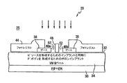
図1に示されるような、従来の横長デバイス設計が半導体材料のN−上部層に形成される。この図は、熱酸化層4を覆って、N−層の表面上に各々形成された一対の離間配置されたゲート電極2を図示している。ゲート電極の間隔は3ミクロンよりも大である。P−型ボディ6は、N−層の表面を通ってゲート電極の間にインプラネーションによって形成される。絶縁側壁スペーサ素子は各ゲート電極2の各側面に形成される。一対のドレイン側壁スペーサ7が図示される。高ドーパント集中ソース領域8がゲート電極2についてオフセット関係にインプラントされるように図示しない一対のソース・スペーサが異なるゲート電極2の対向する側面に形成される。
A conventional landscape device design, as shown in FIG. 1, is formed on the N-top layer of semiconductor material. This figure illustrates a pair of spaced apart
ソース領域8を形成するインプラントと同時に、N+ドレイン10がゲート電極2に対して離間されて、パターン化されたフォトレジスト開口部に形成される。ソース抵抗をより下げるためには、一般的にはソース・スペーサが図示されるように除去されて、低濃度N−型インプラントがゲート電極2と自己配列して軽ドープソース延長領域14を画定する。同時に、残りのドレイン側面スペーサ7について、N−型インプラントが各ドリフト領域の一部、すなわち、各ゲート電極2及び関連ドレイン10の間のN−上部層の体積における固有抵抗を低下させる。材料の固有抵抗の変更は、ドリフト領域を横切る電場(すなわちゲートからドレインまでの電流パス)におけるより大なる均一性の確立に寄与する。
Simultaneously with the implant forming the
図1のデバイス内にインプラントされた領域は、図1Aに示すように3つの分離したコンタクトによって後に接触(コンタクト)せしめられる。N+ソース領域は側壁スペーサの範囲外にある点に注意されたい。2つのN+ソース領域とP+ボディ・タイとをコンタクトするためには、従来のデバイスは3つの分離したコンタクトを使用していた。各コンタクトの面積は工程パラメータによって制限される最小大きさを有する。各コンタクトのコンタクト面積は、1つのコンタクトを他のコンタクトから分離する、例えば二酸化シリコンの如き絶縁体を提供するのに十分広くなければならない。このように、従来のデバイスは、そのゲートの対向する側壁スペーサ間に少なくとも3つの最小コンタクト面積を有するのである。相対的に大なるソースコンタクト面積は、リークや、デバイスのN+ソース領域の下のp−ボディ抵抗を増加させる。 The region implanted in the device of FIG. 1 is subsequently contacted by three separate contacts as shown in FIG. 1A. Note that the N + source region is outside the range of the sidewall spacer. To contact the two N + source regions and the P + body tie, the prior device used three separate contacts. The area of each contact has a minimum size limited by process parameters. The contact area of each contact must be large enough to provide an insulator, such as silicon dioxide, that separates one contact from the other. Thus, conventional devices have at least three minimum contact areas between opposing sidewall spacers of their gates. A relatively large source contact area increases leakage and p-body resistance under the N + source region of the device.
本発明は、3つから1つへソース及びボディ・タイのコンタクト領域の数を減じることで従来技術の不利益を克服する。これは、ゲート構造体の間の間隔を減じて、ソース領域の大きさを減じ、これによりリーク及びp−ボディ抵抗を減じるのである。その結果、本発明によるデバイスは、より大なる安全動作領域を有するのである。 The present invention overcomes the disadvantages of the prior art by reducing the number of source and body tie contact areas from three to one. This reduces the spacing between the gate structures and reduces the size of the source region, thereby reducing leakage and p-body resistance. As a result, the device according to the invention has a larger safe operating area.
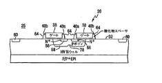
本発明の1つの実施例によるLDMOSペア20の製造方法が図2A乃至2Fに示される集積回路構造体25の部分断面図に示される。0.35ミクロン線幅結合構造に基づくN−チャネルLDMOSにおける関連したステップを順番に示す。上部表面に形成された複数のN−ウェル34を有する上面32を有するP−型半導体層30から始まる。本図は、表面32に沿って形成されたN−チャネル及びP−チャネルLDMOSデバイスを有するCMOS集積回路を表しているが、図示の目的で一対のN−チャネルデバイス20の製造方法について詳述する。すなわち、N−チャネル・デバイス20がN−ウェル内に形成されるとともに、相補的なP−チャネルデバイスが層30のP−型領域において形成されることを理解されるであろう。層30は、図示しない下地基板上にエピタキシャルに成長せしめられる。
A method of manufacturing an
N−型ウェル34に形成された典型的なLDMOSペア20とともに、関連したN−ウェルの重要部分だけが図示される。図2A及び図2Bに関して、一対の離間されたゲート電極38が表層32の上に従来、形成されていた。各電極38は、他の電極38に対抗する端部40aを含み、各電極は、他の電極38とは反対を向いた端部40bを更に含む。図2Bを参照されたい。端部40aの間の好適な幅は、約1ミクロンである。
With a
フォトレジスト44のインプラント・マスク・レベルが堆積されて層30の表面32を覆ってパターン化される。図示した電極38の端部40aの間で間隔を置いて素子48を配置して、2つの離間した開口部52を形成する。その幅はソース・インプラントを受容するのに適しており、典型的には約0.3ミクロンである。レジスト素子48は、インプランテーションの影響から開口部52の間の表面32の充分な領域50を絶縁して、横方向拡散の後のドープ領域の分離を確保することを目的として設けられている。これは、好ましくは0.4ミクロンオーダーの幅を有する。適当なフォトレジスト44を与えられて、ボディ領域を形成するために表面32に沿って浅いN−型ソース・ドーパント及びN−ウェル内により深いP−型ドーパントを与えるようにヘテロドーピングインプラントが行われる。その後、フォトレジスト44が除去される。拡散後のソース56及びボディ領域58の形成を示す図2Bを参照されたい。好ましくは、ボディ領域インプラントは60KeVで5×1013cm-2から1×1014cm-2(ボロン)のオーダーである。一方、ソース・インプラントは30KeVで3×1015cm-2(ヒ素)のオーダーである。分離したフォトマスク及びインプラントステップで形成された従来のN型ドレイン60も図示する。ドレイン60は、表面32の他の部分に沿って、他のCMOSデバイスの形成とともに形成され得る。
An implant mask level of
ソース及びボディ領域インプラントを決定するヘテロドーピングステップの後、図2Cに図示したように側壁スペーサ素子64がゲート端部40aの上に形成される。またゲート端部40bの上にも形成され得る。スペーサ素子64は、異方性エッチングに続いて、例えば酸化シリコンまたは窒化シリコンの如き、絶縁物の堆積によって形成され得る。
After the heterodoping step to determine the source and body region implants,
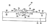
各ゲート端部40aに対向して配置されたスペーサ素子64とともに、ドレイン60を越えてゲート電極端部40bから更に伸びる表面を覆う領域がパターン化されたフォトレジスト66でマスキングされる。図2Dを参照されたい。ここで、表面32の露出部分は、ボディ・タイ70を形成するために、80KeVで1×1015cm-2から3×1015cm-2のオーダー(ボロンまたはBF2)のP+インプラント68を受ける。ボディ・タイは、ソース領域を通って延在し隣接したスペーサ素子64に自己配列する。すなわち、ボディ・タイは、ソースによって占められた表面32の下の領域に繰り込まれる。得られるソース56がボディ・タイ70に関してオフセットされるようなボディ・タイ・インプラントに関して、本発明によればソース・インプラントの横方向オフセットを許容する。拡散後に最終的に得られる構造体において、ボディ・タイが各隣接スペーサ素子64と自己配列する間に各ソースは隣接したゲート端部40aと自己配列される。好ましくは、インプラント68は集積回路構造体25上のデジタル・回路のためのCMOS P+ソース/ドレイン拡散を形成するために使用される。
A region covering the surface extending beyond the
図2Dに示すように、完全に形成されたボディ・タイ70はソース領域56の下で半導体層30に達する。すなわち、ウェル34及びボディ58に達する。この構造の特徴は、繰り込まれたボディ・タイが低い抵抗及び小なる横方向の大きさである一方、スペーサ素子64の下に配置される各ソース56のほとんどの部分は相対的に多量のネットドーパント濃度を保持するのである。フォトレジスト・マスク66の除去の後、金属、例えばタングステン、チタンまたはコバルトが堆積されて、反応によりゲート・シリサイド74及びソース/ボディ・タイ・シリサイド76を形成する。図2Eはシリサイド化工程の後の構造体25を図示している。
As shown in FIG. 2D, the fully formed
改良されたLDMOSデバイスが記載される。得られたデバイスは、改善されたオン抵抗及び動作の安全動作領域を有する。本発明の特徴は、ソース領域56及びボディ領域58を1つのマスク・レベルで与える図2A及び図2Bのヘテロドーピングインプラントである。すなわち、動作特性を改善したLDMOSを形成するために必要なマスクの数を減じたのである。特に、離間された領域50の周囲のソース領域56及び領域50の下のボディ領域の一部分の深さのインフレクション76の組合せにおいてヘテロドーピング形態となる。つまり、これらの特徴のいずれもがヘテロドーピング工程の間のマスク素子48の存在に起因するものである。すなわち、半導体層のボディ領域の深さは、第1の領域の下の深さと比較してゲート電極の下で相対的により深いのである。
An improved LDMOS device is described. The resulting device has improved on-resistance and safe operating area of operation. A feature of the present invention is the heterodoping implant of FIGS. 2A and 2B that provides the
本発明の他の特徴は、第2の導電型の重ドープ領域と、例えば電極38の如き、隣接ゲート構造の下にある半導体層の一部分との間の相対的に一定な横方向ドーパント分布によって特徴づけられるソース領域を供給することである。すなわち、ソース領域はネット導電型の単一のドーパント・インプラントで形成されていてもよい。一方、従来例では、ソース構造はデバイスオン抵抗を下げるために重ドープ領域(例えば図1の領域8)及び軽ドープ領域(例えば図1の延長領域14)の組合せを必要とした。本発明により形成される装置の特に低いオン抵抗は、例えば、図示された自己配列化形成によって達成され得てデバイスユニットの大きさを結果として減じる。動作における改良された安全動作領域は、減じられたボディ抵抗、小なるソース・スペース面積、浅いソース結合及び例えば領域58の如き、ボディ領域の逆行的な添加分布によって生じる。
Another feature of the present invention is the relatively constant lateral dopant distribution between the heavily doped region of the second conductivity type and a portion of the semiconductor layer underneath the adjacent gate structure, such as
改善された動作特性を与える小なる大きさの効果として、例えばゲート電極端部40a及び40bに隣接したスペーサ64の如き、スペーサ素子に微細線結合構造マスクを与えて、小なるソース領域の達成が可能となる。加えて、自己配列化ケイ素化(サリサイド)工程が、例えばボディ・タイ領域及びソース領域の如き、臨界コンタクト領域において多量ドーパント補償を有さない故に、接触抵抗を低くすることが可能なのである。ボディ・タイ70及び関連シリサイド層76は、ソース領域56に関して整列配置される。本発明は、N+ソース・インプラントは同じサイズ及びドレイン・インプラントである必要はないと認識される。
A small size effect that provides improved operating characteristics can be achieved by providing a fine line coupling structure mask to the spacer elements, such as
本発明は、ゲート上に側壁酸化物スペーサを使用することで、P+タイ・インプラントからN+ソース・インプラントをマスキングする。本発明では、N+ソース・インプラントは、側壁スペーサよりも前に形成される。本発明の方法は、1回のマスキング・ステップでN+ソース及びP−ボディをインプラントする。本発明は、従来技術によって必要とされた分離したPボディマスク工程を必要としない。本発明は、2つのN+ソース、P+ボディ・タイ及びN+ソースとP+ボディ・タイとのオーバーラップに自己配列した1つのシリサイドコンタクトを与える。コンタクトの数は、従来の3から1まで減じられる。ゲート間に1つのコンタクトを設けることで、より密度の高いデバイスを提供する。そして、このデバイスは小さなソースによって、より少ないリークとなることから、より広い安全動作領域を有するのである。従来のデバイスのより大なるソースよりも下にp−ボディ抵抗を有する。 The present invention masks the N + source implant from the P + tie implant by using sidewall oxide spacers on the gate. In the present invention, the N + source implant is formed before the sidewall spacer. The method of the present invention implants N + source and P-body in a single masking step. The present invention does not require a separate P body mask process as required by the prior art. The present invention provides one silicide contact that is self-aligned in the overlap of two N + sources, P + body tie and N + source and P + body tie. The number of contacts is reduced from the conventional 3 to 1. By providing one contact between the gates, a higher density device is provided. And this device has a wider safe operating area because it has less leakage with a small source. It has a p-body resistance below the larger source of conventional devices.
改良された半導体デバイスについて構造及び工程を記載してきた。典型的な実施例を開示してきたが、異なる半導体、絶縁性材料及び導電性材料からなる構造を含む本発明の他の実施例も明らかであろう。更に、本発明は導電型の1つの組を図示したが、本発明の応用例は反対の導電型デバイスについても同様に考慮される。本発明はさまざまな方法によって実行され得るが、本発明の範囲は、特許請求の範囲によってのみ限定される。 The structure and process have been described for an improved semiconductor device. While exemplary embodiments have been disclosed, other embodiments of the invention that include structures of different semiconductors, insulating materials, and conductive materials will be apparent. Furthermore, although the present invention illustrates one set of conductivity types, applications of the present invention are equally contemplated for opposite conductivity type devices. The present invention may be implemented in a variety of ways, but the scope of the present invention is limited only by the claims.
Claims (27)
前記半導体層の表面に離間して配置されて一方のゲート構造体が他方のゲート構造体に対向した第1の端部領域を有する一対の電界効果ゲート構造体と、
前記一対のゲート構造体の間の前記半導体層の一部に形成された第1の導電型の第1及び第2の離間されたソース領域と、
前記ソース領域の下から前記ゲート構造体の下まで延在する前記半導体層内の第2の導電型の軽ドープボディ領域と、
前記第1の端部領域の間の前記表面の一部において延在する第2の導電型の重ドープ領域と、を含む半導体デバイスであって、
前記ソース領域の各々は前記第1の端部領域のうちの1に関して自己配列せしめられており、前記第1の端部領域の間の前記表面の一部は第1の面積を有するとともに前記重ドープ領域は前記第1の面積未満の前記表面に沿った面積を有することを特徴とする半導体デバイス。 A semiconductor layer;
A pair of field effect gate structures having a first end region that is spaced apart from the surface of the semiconductor layer and wherein one gate structure faces the other gate structure;
First and second spaced apart source regions of a first conductivity type formed in a portion of the semiconductor layer between the pair of gate structures;
A lightly doped body region of a second conductivity type in the semiconductor layer extending from below the source region to below the gate structure;
A heavily doped region of a second conductivity type extending in a portion of the surface between the first end regions, the semiconductor device comprising:
Each of the source regions is self-aligned with respect to one of the first end regions, and a portion of the surface between the first end regions has a first area and the overlap. The semiconductor device, wherein the doped region has an area along the surface that is less than the first area.
他のゲート構造体に対向した第1の端部領域を含み半導体層の表面上において離間された一対の電界効果ゲート構造体を第1マスク・レベルで形成するステップと、
前記層内であって且つ一対の前記構造体の間に第1の導電型の第1及び第2の離間されたソース領域を第2マスクレベルで形成して前記第1及び第2の離間されたソース領域間の前記表面の得られた領域に第1の面積を与えるステップと、
前記第2のマスク・レベルで前記層内であって且つ前記ソース領域の下に延在する第2の導電型の軽ドープボディ領域を形成するステップと、
前記第1の面積の表面を有する前記半導体層の一部であって、前記第1の面積よりも小なる面積の表面を有する前記一部に前記第2の導電型の重ドープ領域を形成するステップと、を含むことを特徴とする半導体デバイスの製造方法。 Providing a layer of semiconductor material;
Forming a pair of field effect gate structures at a first mask level including a first end region opposite the other gate structure and spaced apart on a surface of the semiconductor layer;
The first and second spaced apart source regions of the first conductivity type are formed at a second mask level in the layer and between the pair of structures. Providing a first area to the resulting region of the surface between the source regions;
Forming a lightly doped body region of a second conductivity type in the layer at the second mask level and extending below the source region;
A heavy doped region of the second conductivity type is formed in a part of the semiconductor layer having a surface having the first area and having a surface having an area smaller than the first area. And a step of manufacturing a semiconductor device.
半導体層と、
前記半導体層の上部表面を覆う一対の離間された電界効果ゲート構造体と、
第2の導電型の第1の領域を有する一対の前記ゲート構造体の間の前記層の一部の第1の導電型の第1及び第2の離間されたソース領域と、
前記ソース領域の下から前記ゲート構造体の下まで延在し、前記半導体層内の可変深さにまで延在し、前記第1の領域の下に延在する前記ボディ領域の一部の前記ボディ領域の深さのインフレクションによって特徴づけられる前記半導体層の第2の導電型の軽ドープボディ領域と、を含むことを特徴とする半導体IC。 A semiconductor IC including an LDMOS device structure,
A semiconductor layer;
A pair of spaced field effect gate structures covering an upper surface of the semiconductor layer;
A first conductive type first and second spaced source region of a portion of the layer between a pair of the gate structures having a first conductive type first region;
The portion of the body region that extends from below the source region to below the gate structure, extends to a variable depth in the semiconductor layer, and extends below the first region. And a lightly doped body region of the second conductivity type of the semiconductor layer characterized by the depth of the body region.
他のゲート構造体に対向する絶縁側壁端部領域を含む前記半導体層の表面上において離間された一対の電界効果ゲート構造体と、
前記一対のゲート構造体の間の前記層の一部の第1の導電型の第1及び第2の離間された重ドープソース領域と、
前記ソース領域の下から前記ゲート構造体の下まで延在する前記半導体層内の第2の導電型の軽ドープボディ領域と、
前記第1の端部領域間の前記表面の前記一部に延在する前記第2の導電型の重ドープボディ・タイ領域と、
前記重ドープソース領域及び前記ボディ・タイ領域の共通シリサイドコンタクトと、を含む半導体デバイスであって、
前記表面の一部は第1の面積を有する絶縁側壁端部の間にあって、各ソース領域は前記絶縁側壁端部領域のうちの1に関して自己配列せしめられて、前記重ドープボディ・タイ領域は前記第1面積未満の前記表面に沿った面積を有することを特徴とする半導体デバイス。 A semiconductor layer;
A pair of field effect gate structures spaced apart on the surface of the semiconductor layer including insulating sidewall end regions opposite the other gate structures;
First and second spaced heavily doped source regions of a first conductivity type of a portion of the layer between the pair of gate structures;
A lightly doped body region of a second conductivity type in the semiconductor layer extending from below the source region to below the gate structure;
A heavily doped body tie region of the second conductivity type extending to the portion of the surface between the first end regions;
A semiconductor device comprising a common silicide contact of the heavily doped source region and the body tie region,
A portion of the surface is between insulating sidewall end portions having a first area, each source region is self-aligned with respect to one of the insulating sidewall end regions, and the heavily doped body tie region is A semiconductor device having an area along the surface of less than a first area.
Applications Claiming Priority (2)
| Application Number | Priority Date | Filing Date | Title |
|---|---|---|---|
| US10/315,517 US6870218B2 (en) | 2002-12-10 | 2002-12-10 | Integrated circuit structure with improved LDMOS design |
| PCT/US2003/038931 WO2004053939A2 (en) | 2002-12-10 | 2003-12-09 | Integrated circuit structure with improved ldmos design |
Publications (2)
| Publication Number | Publication Date |
|---|---|
| JP2006510206A true JP2006510206A (en) | 2006-03-23 |
| JP2006510206A5 JP2006510206A5 (en) | 2011-09-29 |
Family
ID=32468724
Family Applications (1)
| Application Number | Title | Priority Date | Filing Date |
|---|---|---|---|
| JP2004559410A Pending JP2006510206A (en) | 2002-12-10 | 2003-12-09 | Integrated circuit structure |
Country Status (8)
| Country | Link |
|---|---|
| US (3) | US6870218B2 (en) |
| JP (1) | JP2006510206A (en) |
| KR (1) | KR101030178B1 (en) |
| CN (1) | CN100524812C (en) |
| AU (1) | AU2003296321A1 (en) |
| DE (1) | DE10393858T5 (en) |
| TW (1) | TWI355074B (en) |
| WO (1) | WO2004053939A2 (en) |
Cited By (2)
| Publication number | Priority date | Publication date | Assignee | Title |
|---|---|---|---|---|
| JP2009260155A (en) * | 2008-04-21 | 2009-11-05 | Sanyo Electric Co Ltd | Dmos transistor |
| JP2012156205A (en) * | 2011-01-24 | 2012-08-16 | Asahi Kasei Electronics Co Ltd | Semiconductor device, method of manufacturing the same |
Families Citing this family (23)
| Publication number | Priority date | Publication date | Assignee | Title |
|---|---|---|---|---|
| US6870218B2 (en) * | 2002-12-10 | 2005-03-22 | Fairchild Semiconductor Corporation | Integrated circuit structure with improved LDMOS design |
| JP4800566B2 (en) * | 2003-10-06 | 2011-10-26 | ルネサスエレクトロニクス株式会社 | Semiconductor device and manufacturing method thereof |
| US7180132B2 (en) * | 2004-09-16 | 2007-02-20 | Fairchild Semiconductor Corporation | Enhanced RESURF HVPMOS device with stacked hetero-doping RIM and gradual drift region |
| JP4907920B2 (en) * | 2005-08-18 | 2012-04-04 | 株式会社東芝 | Semiconductor device and manufacturing method thereof |
| US7736984B2 (en) * | 2005-09-23 | 2010-06-15 | Semiconductor Components Industries, Llc | Method of forming a low resistance semiconductor contact and structure therefor |
| CN100370625C (en) * | 2005-10-14 | 2008-02-20 | 西安电子科技大学 | Integrated high-voltage P-type LDMOS transistor structure and production thereof |
| KR100778861B1 (en) * | 2006-12-12 | 2007-11-22 | 동부일렉트로닉스 주식회사 | Method for fabricating ldmos semiconductor device |
| US8035159B2 (en) * | 2007-04-30 | 2011-10-11 | Alpha & Omega Semiconductor, Ltd. | Device structure and manufacturing method using HDP deposited source-body implant block |
| KR100840667B1 (en) * | 2007-06-26 | 2008-06-24 | 주식회사 동부하이텍 | Lateral dmos device and fabrication method therefor |
| US8063443B2 (en) | 2007-10-30 | 2011-11-22 | Fairchild Semiconductor Corporation | Hybrid-mode LDMOS |
| US7906810B2 (en) * | 2008-08-06 | 2011-03-15 | United Microelectronics Corp. | LDMOS device for ESD protection circuit |
| US8138558B2 (en) * | 2010-08-20 | 2012-03-20 | Great Wall Semiconductor Corporation | Semiconductor device and method of forming low voltage MOSFET for portable electronic devices and data processing centers |
| CN102681370B (en) * | 2012-05-09 | 2016-04-20 | 上海华虹宏力半导体制造有限公司 | Photoetching overlay method and raising LDMOS device puncture the method for stability |
| CN103456734B (en) * | 2012-05-28 | 2016-04-13 | 上海华虹宏力半导体制造有限公司 | A kind of monitoring structure of asymmetric LDMOS process deviation and manufacture method thereof |
| US9337284B2 (en) * | 2014-04-07 | 2016-05-10 | Alpha And Omega Semiconductor Incorporated | Closed cell lateral MOSFET using silicide source and body regions |
| US10038063B2 (en) | 2014-06-10 | 2018-07-31 | International Business Machines Corporation | Tunable breakdown voltage RF FET devices |
| US9397090B1 (en) * | 2015-04-10 | 2016-07-19 | Macronix International Co., Ltd. | Semiconductor device |
| CN108493113A (en) * | 2018-03-30 | 2018-09-04 | 北京时代民芯科技有限公司 | A kind of manufacturing method of low resistance Flouride-resistani acid phesphatase VDMOS chip |
| TWI666681B (en) * | 2018-07-18 | 2019-07-21 | 帥群微電子股份有限公司 | Semiconductor power device and manufacturing method thereof |
| US20210020630A1 (en) * | 2019-04-15 | 2021-01-21 | Nexchip Semiconductor Co., Ltd. | High-voltage tolerant semiconductor element |
| CN111200020B (en) * | 2019-04-15 | 2021-01-08 | 合肥晶合集成电路股份有限公司 | High voltage semiconductor device and method for manufacturing the same |
| US11581215B2 (en) * | 2020-07-14 | 2023-02-14 | Newport Fab, Llc | Body-source-tied semiconductor-on-insulator (SOI) transistor |
| CN116207142B (en) * | 2023-05-04 | 2023-07-18 | 合肥晶合集成电路股份有限公司 | Semiconductor structure and manufacturing method thereof |
Citations (8)
| Publication number | Priority date | Publication date | Assignee | Title |
|---|---|---|---|---|
| JPS5578574A (en) * | 1978-12-09 | 1980-06-13 | Victor Co Of Japan Ltd | Manufacture of insulated-gate field-effect transistor |
| US4883767A (en) * | 1986-12-05 | 1989-11-28 | General Electric Company | Method of fabricating self aligned semiconductor devices |
| JPH03244135A (en) * | 1990-02-22 | 1991-10-30 | New Japan Radio Co Ltd | Manufacture of mos transistor |
| JPH0897410A (en) * | 1994-07-01 | 1996-04-12 | Texas Instr Inc <Ti> | Manufacture of lateral type dmos transistor that self conforms |
| EP0747966A2 (en) * | 1995-06-07 | 1996-12-11 | Harris Corporation | High efficiency quasi-vertical DMOS in MOS or BICMOS process |
| JPH10335663A (en) * | 1997-05-23 | 1998-12-18 | Texas Instr Inc <Ti> | Reduced surface drain(rsd) ldmos power device |
| US6049104A (en) * | 1997-11-28 | 2000-04-11 | Magepower Semiconductor Corp. | MOSFET device to reduce gate-width without increasing JFET resistance |
| JP2002314065A (en) * | 2001-04-13 | 2002-10-25 | Sanyo Electric Co Ltd | Mos semiconductor device and its manufacturing method |
Family Cites Families (30)
| Publication number | Priority date | Publication date | Assignee | Title |
|---|---|---|---|---|
| US5079608A (en) | 1990-11-06 | 1992-01-07 | Harris Corporation | Power MOSFET transistor circuit with active clamp |
| US5272098A (en) * | 1990-11-21 | 1993-12-21 | Texas Instruments Incorporated | Vertical and lateral insulated-gate, field-effect transistors, systems and methods |
| CN1019720B (en) | 1991-03-19 | 1992-12-30 | 电子科技大学 | Power semiconductor device |
| US5585294A (en) * | 1994-10-14 | 1996-12-17 | Texas Instruments Incorporated | Method of fabricating lateral double diffused MOS (LDMOS) transistors |
| EP0730309B1 (en) * | 1995-02-21 | 1998-10-14 | STMicroelectronics S.r.l. | A high voltage MOSFET structure with field plate electrode and process for its fabrication |
| US5567634A (en) * | 1995-05-01 | 1996-10-22 | National Semiconductor Corporation | Method of fabricating self-aligned contact trench DMOS transistors |
| EP0741416B1 (en) * | 1995-05-02 | 2001-09-26 | STMicroelectronics S.r.l. | Thin epitaxy RESURF ic containing HV p-ch and n-ch devices with source or drain not tied to grounds potential |
| KR0143459B1 (en) * | 1995-05-22 | 1998-07-01 | 한민구 | Morse-gate type power transistor |
| US5684319A (en) * | 1995-08-24 | 1997-11-04 | National Semiconductor Corporation | Self-aligned source and body contact structure for high performance DMOS transistors and method of fabricating same |
| JP3528420B2 (en) * | 1996-04-26 | 2004-05-17 | 株式会社デンソー | Semiconductor device and manufacturing method thereof |
| US5792687A (en) * | 1996-08-01 | 1998-08-11 | Vanguard International Semiconductor Corporation | Method for fabricating high density integrated circuits using oxide and polysilicon spacers |
| US5960275A (en) * | 1996-10-28 | 1999-09-28 | Magemos Corporation | Power MOSFET fabrication process to achieve enhanced ruggedness, cost savings, and product reliability |
| US5879968A (en) * | 1996-11-18 | 1999-03-09 | International Rectifier Corporation | Process for manufacture of a P-channel MOS gated device with base implant through the contact window |
| KR100204805B1 (en) * | 1996-12-28 | 1999-06-15 | 윤종용 | Method for fabricating transistor |
| KR100225411B1 (en) * | 1997-03-24 | 1999-10-15 | 김덕중 | Ldmos transistor device and method of manufacturing the same |
| US5907169A (en) * | 1997-04-18 | 1999-05-25 | Megamos Corporation | Self-aligned and process-adjusted high density power transistor with gate sidewalls provided with punch through prevention and reduced JFET resistance |
| US5854099A (en) * | 1997-06-06 | 1998-12-29 | National Semiconductor Corporation | DMOS process module applicable to an E2 CMOS core process |
| US5930630A (en) * | 1997-07-23 | 1999-07-27 | Megamos Corporation | Method for device ruggedness improvement and on-resistance reduction for power MOSFET achieved by novel source contact structure |
| US6252278B1 (en) | 1998-05-18 | 2001-06-26 | Monolithic Power Systems, Inc. | Self-aligned lateral DMOS with spacer drift region |
| KR100301071B1 (en) * | 1998-10-26 | 2001-11-22 | 김덕중 | DMOS transistor and method for manufacturing thereof |
| JP2000208759A (en) * | 1999-01-12 | 2000-07-28 | Rohm Co Ltd | Semiconductor device |
| KR20000051294A (en) * | 1999-01-20 | 2000-08-16 | 김덕중 | DMOS field effect transistor with improved electrical characteristics and fabricating method thereof |
| US6277695B1 (en) * | 1999-04-16 | 2001-08-21 | Siliconix Incorporated | Method of forming vertical planar DMOSFET with self-aligned contact |
| US6198127B1 (en) | 1999-05-19 | 2001-03-06 | Intersil Corporation | MOS-gated power device having extended trench and doping zone and process for forming same |
| US6365932B1 (en) * | 1999-08-20 | 2002-04-02 | Denso Corporation | Power MOS transistor |
| US6376878B1 (en) | 2000-02-11 | 2002-04-23 | Fairchild Semiconductor Corporation | MOS-gated devices with alternating zones of conductivity |
| US7115946B2 (en) * | 2000-09-28 | 2006-10-03 | Kabushiki Kaisha Toshiba | MOS transistor having an offset region |
| JP3431909B2 (en) * | 2001-08-21 | 2003-07-28 | 沖電気工業株式会社 | LDMOS transistor manufacturing method |
| US6661042B2 (en) * | 2002-03-11 | 2003-12-09 | Monolithic System Technology, Inc. | One-transistor floating-body DRAM cell in bulk CMOS process with electrically isolated charge storage region |
| US6870218B2 (en) * | 2002-12-10 | 2005-03-22 | Fairchild Semiconductor Corporation | Integrated circuit structure with improved LDMOS design |
-
2002
- 2002-12-10 US US10/315,517 patent/US6870218B2/en not_active Expired - Fee Related
-
2003
- 2003-12-09 WO PCT/US2003/038931 patent/WO2004053939A2/en active Application Filing
- 2003-12-09 KR KR1020057010197A patent/KR101030178B1/en not_active IP Right Cessation
- 2003-12-09 AU AU2003296321A patent/AU2003296321A1/en not_active Abandoned
- 2003-12-09 JP JP2004559410A patent/JP2006510206A/en active Pending
- 2003-12-09 TW TW092134753A patent/TWI355074B/en not_active IP Right Cessation
- 2003-12-09 DE DE10393858T patent/DE10393858T5/en not_active Withdrawn
- 2003-12-09 CN CNB2003801057172A patent/CN100524812C/en not_active Expired - Fee Related
-
2005
- 2005-03-01 US US11/069,900 patent/US7220646B2/en not_active Expired - Lifetime
-
2007
- 2007-02-16 US US11/675,759 patent/US7608512B2/en not_active Expired - Fee Related
Patent Citations (8)
| Publication number | Priority date | Publication date | Assignee | Title |
|---|---|---|---|---|
| JPS5578574A (en) * | 1978-12-09 | 1980-06-13 | Victor Co Of Japan Ltd | Manufacture of insulated-gate field-effect transistor |
| US4883767A (en) * | 1986-12-05 | 1989-11-28 | General Electric Company | Method of fabricating self aligned semiconductor devices |
| JPH03244135A (en) * | 1990-02-22 | 1991-10-30 | New Japan Radio Co Ltd | Manufacture of mos transistor |
| JPH0897410A (en) * | 1994-07-01 | 1996-04-12 | Texas Instr Inc <Ti> | Manufacture of lateral type dmos transistor that self conforms |
| EP0747966A2 (en) * | 1995-06-07 | 1996-12-11 | Harris Corporation | High efficiency quasi-vertical DMOS in MOS or BICMOS process |
| JPH10335663A (en) * | 1997-05-23 | 1998-12-18 | Texas Instr Inc <Ti> | Reduced surface drain(rsd) ldmos power device |
| US6049104A (en) * | 1997-11-28 | 2000-04-11 | Magepower Semiconductor Corp. | MOSFET device to reduce gate-width without increasing JFET resistance |
| JP2002314065A (en) * | 2001-04-13 | 2002-10-25 | Sanyo Electric Co Ltd | Mos semiconductor device and its manufacturing method |
Cited By (2)
| Publication number | Priority date | Publication date | Assignee | Title |
|---|---|---|---|---|
| JP2009260155A (en) * | 2008-04-21 | 2009-11-05 | Sanyo Electric Co Ltd | Dmos transistor |
| JP2012156205A (en) * | 2011-01-24 | 2012-08-16 | Asahi Kasei Electronics Co Ltd | Semiconductor device, method of manufacturing the same |
Also Published As
| Publication number | Publication date |
|---|---|
| CN100524812C (en) | 2009-08-05 |
| KR101030178B1 (en) | 2011-04-18 |
| CN1757118A (en) | 2006-04-05 |
| TW200503266A (en) | 2005-01-16 |
| AU2003296321A8 (en) | 2004-06-30 |
| US20070141792A1 (en) | 2007-06-21 |
| WO2004053939A2 (en) | 2004-06-24 |
| US20050239253A1 (en) | 2005-10-27 |
| AU2003296321A1 (en) | 2004-06-30 |
| US6870218B2 (en) | 2005-03-22 |
| KR20050085383A (en) | 2005-08-29 |
| DE10393858T5 (en) | 2007-03-15 |
| US20040108548A1 (en) | 2004-06-10 |
| TWI355074B (en) | 2011-12-21 |
| US7608512B2 (en) | 2009-10-27 |
| US7220646B2 (en) | 2007-05-22 |
| WO2004053939A3 (en) | 2005-07-21 |
Similar Documents
| Publication | Publication Date | Title |
|---|---|---|
| US7220646B2 (en) | Integrated circuit structure with improved LDMOS design | |
| US7125777B2 (en) | Asymmetric hetero-doped high-voltage MOSFET (AH2MOS) | |
| US6277675B1 (en) | Method of fabricating high voltage MOS device | |
| US7687335B2 (en) | Self aligned gate JFET structure and method | |
| US6833586B2 (en) | LDMOS transistor with high voltage source and drain terminals | |
| JP4384224B2 (en) | High voltage junction field effect transistor | |
| JPH11284174A (en) | Field connection-type power mosfet bus architecture using trench technology | |
| US20120187476A1 (en) | Semiconductor device and method of manufacturing the same | |
| KR100611111B1 (en) | High Frequency MOS Transistor, Method of forming the same and Method of manufacturing semiconductor device | |
| US7560324B2 (en) | Drain extended MOS transistors and methods for making the same | |
| JPH1084045A (en) | Semiconductor integrated circuit device and its manufacturing method | |
| JPH11330267A (en) | Assembly of double supply voltage by excluding drain extender injection from high voltage | |
| EP1142014B1 (en) | A method of manufacturing a peripheral transistor of a non-volatile memory | |
| US20100090291A1 (en) | Transistor structure having reduced input capacitance | |
| US8354716B2 (en) | Semiconductor devices and methods of manufacturing the same | |
| US7928445B2 (en) | Semiconductor MOS transistor device | |
| US7364959B2 (en) | Method for manufacturing a MOS transistor | |
| US20230136827A1 (en) | Laterally difused metal-oxide semiconductor (ldmos) transistor with integrated back-gate | |
| KR0165347B1 (en) | Transistor with high breakdown voltage and method of making thereof | |
| US5970349A (en) | Semiconductor device having one or more asymmetric background dopant regions and method of manufacture thereof | |
| KR101201496B1 (en) | Lateral diffused metal oxide semiconductor and method for manufacturing the same | |
| US20040166625A1 (en) | Method for increasing the Beta of PNP BJT device in CMOS process |
Legal Events
| Date | Code | Title | Description |
|---|---|---|---|
| A621 | Written request for application examination |
Free format text: JAPANESE INTERMEDIATE CODE: A621 Effective date: 20061124 |
|
| A977 | Report on retrieval |
Free format text: JAPANESE INTERMEDIATE CODE: A971007 Effective date: 20090326 |
|
| A131 | Notification of reasons for refusal |
Free format text: JAPANESE INTERMEDIATE CODE: A131 Effective date: 20100629 |
|
| A601 | Written request for extension of time |
Free format text: JAPANESE INTERMEDIATE CODE: A601 Effective date: 20100921 |
|
| A602 | Written permission of extension of time |
Free format text: JAPANESE INTERMEDIATE CODE: A602 Effective date: 20100929 |
|
| A521 | Request for written amendment filed |
Free format text: JAPANESE INTERMEDIATE CODE: A523 Effective date: 20101228 |
|
| A131 | Notification of reasons for refusal |
Free format text: JAPANESE INTERMEDIATE CODE: A131 Effective date: 20110510 |
|
| A524 | Written submission of copy of amendment under article 19 pct |
Free format text: JAPANESE INTERMEDIATE CODE: A524 Effective date: 20110809 |
|
| A02 | Decision of refusal |
Free format text: JAPANESE INTERMEDIATE CODE: A02 Effective date: 20120214 |