JP2006509375A - Multilayer gate stack - Google Patents
Multilayer gate stack Download PDFInfo
- Publication number
- JP2006509375A JP2006509375A JP2004559293A JP2004559293A JP2006509375A JP 2006509375 A JP2006509375 A JP 2006509375A JP 2004559293 A JP2004559293 A JP 2004559293A JP 2004559293 A JP2004559293 A JP 2004559293A JP 2006509375 A JP2006509375 A JP 2006509375A
- Authority
- JP
- Japan
- Prior art keywords
- layer
- gate
- nitride layer
- semiconductor
- sccm
- Prior art date
- Legal status (The legal status is an assumption and is not a legal conclusion. Google has not performed a legal analysis and makes no representation as to the accuracy of the status listed.)
- Pending
Links
- 239000004065 semiconductor Substances 0.000 claims abstract description 52
- 150000004767 nitrides Chemical class 0.000 claims abstract description 49
- 238000005530 etching Methods 0.000 claims abstract description 41
- 229920002120 photoresistant polymer Polymers 0.000 claims abstract description 28
- 239000000758 substrate Substances 0.000 claims abstract description 26
- 239000000203 mixture Substances 0.000 claims abstract description 16
- 238000004519 manufacturing process Methods 0.000 claims abstract description 10
- 238000000034 method Methods 0.000 claims description 40
- 229910052751 metal Inorganic materials 0.000 claims description 27
- 239000002184 metal Substances 0.000 claims description 27
- 239000007789 gas Substances 0.000 claims description 19
- 229910052710 silicon Inorganic materials 0.000 claims description 11
- 239000010703 silicon Substances 0.000 claims description 11
- 229910052739 hydrogen Inorganic materials 0.000 claims description 8
- UFHFLCQGNIYNRP-UHFFFAOYSA-N Hydrogen Chemical compound [H][H] UFHFLCQGNIYNRP-UHFFFAOYSA-N 0.000 claims description 7
- 239000001257 hydrogen Substances 0.000 claims description 7
- 238000002955 isolation Methods 0.000 claims description 7
- 239000011737 fluorine Substances 0.000 claims description 5
- 229910052731 fluorine Inorganic materials 0.000 claims description 5
- OKTJSMMVPCPJKN-UHFFFAOYSA-N Carbon Chemical compound [C] OKTJSMMVPCPJKN-UHFFFAOYSA-N 0.000 claims description 3
- 229910052799 carbon Inorganic materials 0.000 claims description 3
- PXGOKWXKJXAPGV-UHFFFAOYSA-N Fluorine Chemical compound FF PXGOKWXKJXAPGV-UHFFFAOYSA-N 0.000 claims 1
- 238000000926 separation method Methods 0.000 claims 1
- 239000010410 layer Substances 0.000 description 139
- 229910052721 tungsten Inorganic materials 0.000 description 15
- 239000010937 tungsten Substances 0.000 description 15
- 230000015572 biosynthetic process Effects 0.000 description 14
- 238000004140 cleaning Methods 0.000 description 14
- CPELXLSAUQHCOX-UHFFFAOYSA-N Hydrogen bromide Chemical compound Br CPELXLSAUQHCOX-UHFFFAOYSA-N 0.000 description 12
- 230000004888 barrier function Effects 0.000 description 11
- 125000006850 spacer group Chemical group 0.000 description 11
- WFKWXMTUELFFGS-UHFFFAOYSA-N tungsten Chemical compound [W] WFKWXMTUELFFGS-UHFFFAOYSA-N 0.000 description 11
- XUIMIQQOPSSXEZ-UHFFFAOYSA-N Silicon Chemical compound [Si] XUIMIQQOPSSXEZ-UHFFFAOYSA-N 0.000 description 9
- 239000000463 material Substances 0.000 description 8
- 229910052581 Si3N4 Inorganic materials 0.000 description 6
- 229910000042 hydrogen bromide Inorganic materials 0.000 description 6
- HQVNEWCFYHHQES-UHFFFAOYSA-N silicon nitride Chemical compound N12[Si]34N5[Si]62N3[Si]51N64 HQVNEWCFYHHQES-UHFFFAOYSA-N 0.000 description 6
- XLYOFNOQVPJJNP-UHFFFAOYSA-N water Substances O XLYOFNOQVPJJNP-UHFFFAOYSA-N 0.000 description 6
- 238000004380 ashing Methods 0.000 description 5
- 239000002019 doping agent Substances 0.000 description 5
- YCKRFDGAMUMZLT-UHFFFAOYSA-N Fluorine atom Chemical compound [F] YCKRFDGAMUMZLT-UHFFFAOYSA-N 0.000 description 4
- YCIMNLLNPGFGHC-UHFFFAOYSA-N catechol Chemical compound OC1=CC=CC=C1O YCIMNLLNPGFGHC-UHFFFAOYSA-N 0.000 description 4
- 150000003377 silicon compounds Chemical class 0.000 description 4
- -1 tungsten nitride Chemical class 0.000 description 4
- 235000012431 wafers Nutrition 0.000 description 4
- RTAQQCXQSZGOHL-UHFFFAOYSA-N Titanium Chemical compound [Ti] RTAQQCXQSZGOHL-UHFFFAOYSA-N 0.000 description 3
- 239000000460 chlorine Substances 0.000 description 3
- 239000008367 deionised water Substances 0.000 description 3
- 229910021641 deionized water Inorganic materials 0.000 description 3
- 230000000694 effects Effects 0.000 description 3
- 238000005516 engineering process Methods 0.000 description 3
- 230000003647 oxidation Effects 0.000 description 3
- 238000007254 oxidation reaction Methods 0.000 description 3
- 229910021420 polycrystalline silicon Inorganic materials 0.000 description 3
- 230000005855 radiation Effects 0.000 description 3
- 239000010936 titanium Substances 0.000 description 3
- 229910052719 titanium Inorganic materials 0.000 description 3
- 238000005406 washing Methods 0.000 description 3
- XKRFYHLGVUSROY-UHFFFAOYSA-N Argon Chemical compound [Ar] XKRFYHLGVUSROY-UHFFFAOYSA-N 0.000 description 2
- 241000282461 Canis lupus Species 0.000 description 2
- KRHYYFGTRYWZRS-UHFFFAOYSA-N Fluorane Chemical compound F KRHYYFGTRYWZRS-UHFFFAOYSA-N 0.000 description 2
- XPDWGBQVDMORPB-UHFFFAOYSA-N Fluoroform Chemical compound FC(F)F XPDWGBQVDMORPB-UHFFFAOYSA-N 0.000 description 2
- AVXURJPOCDRRFD-UHFFFAOYSA-N Hydroxylamine Chemical compound ON AVXURJPOCDRRFD-UHFFFAOYSA-N 0.000 description 2
- QAOWNCQODCNURD-UHFFFAOYSA-N Sulfuric acid Chemical compound OS(O)(=O)=O QAOWNCQODCNURD-UHFFFAOYSA-N 0.000 description 2
- 229910045601 alloy Inorganic materials 0.000 description 2
- 239000000956 alloy Substances 0.000 description 2
- QVGXLLKOCUKJST-UHFFFAOYSA-N atomic oxygen Chemical compound [O] QVGXLLKOCUKJST-UHFFFAOYSA-N 0.000 description 2
- 238000005229 chemical vapour deposition Methods 0.000 description 2
- 239000004020 conductor Substances 0.000 description 2
- 230000007423 decrease Effects 0.000 description 2
- 238000000151 deposition Methods 0.000 description 2
- 230000008021 deposition Effects 0.000 description 2
- 239000003599 detergent Substances 0.000 description 2
- 238000009792 diffusion process Methods 0.000 description 2
- RWRIWBAIICGTTQ-UHFFFAOYSA-N difluoromethane Chemical compound FCF RWRIWBAIICGTTQ-UHFFFAOYSA-N 0.000 description 2
- 239000004744 fabric Substances 0.000 description 2
- 238000004518 low pressure chemical vapour deposition Methods 0.000 description 2
- 230000000873 masking effect Effects 0.000 description 2
- 229910044991 metal oxide Inorganic materials 0.000 description 2
- 150000004706 metal oxides Chemical class 0.000 description 2
- 238000001465 metallisation Methods 0.000 description 2
- 229910052760 oxygen Inorganic materials 0.000 description 2
- 239000001301 oxygen Substances 0.000 description 2
- 238000005240 physical vapour deposition Methods 0.000 description 2
- 238000001020 plasma etching Methods 0.000 description 2
- 238000000623 plasma-assisted chemical vapour deposition Methods 0.000 description 2
- 229910052715 tantalum Inorganic materials 0.000 description 2
- GUVRBAGPIYLISA-UHFFFAOYSA-N tantalum atom Chemical compound [Ta] GUVRBAGPIYLISA-UHFFFAOYSA-N 0.000 description 2
- IHGSAQHSAGRWNI-UHFFFAOYSA-N 1-(4-bromophenyl)-2,2,2-trifluoroethanone Chemical compound FC(F)(F)C(=O)C1=CC=C(Br)C=C1 IHGSAQHSAGRWNI-UHFFFAOYSA-N 0.000 description 1
- BMYNFMYTOJXKLE-UHFFFAOYSA-N 3-azaniumyl-2-hydroxypropanoate Chemical compound NCC(O)C(O)=O BMYNFMYTOJXKLE-UHFFFAOYSA-N 0.000 description 1
- JBRZTFJDHDCESZ-UHFFFAOYSA-N AsGa Chemical compound [As]#[Ga] JBRZTFJDHDCESZ-UHFFFAOYSA-N 0.000 description 1
- ZAMOUSCENKQFHK-UHFFFAOYSA-N Chlorine atom Chemical compound [Cl] ZAMOUSCENKQFHK-UHFFFAOYSA-N 0.000 description 1
- RYGMFSIKBFXOCR-UHFFFAOYSA-N Copper Chemical compound [Cu] RYGMFSIKBFXOCR-UHFFFAOYSA-N 0.000 description 1
- 229910002601 GaN Inorganic materials 0.000 description 1
- 229910001218 Gallium arsenide Inorganic materials 0.000 description 1
- JMASRVWKEDWRBT-UHFFFAOYSA-N Gallium nitride Chemical compound [Ga]#N JMASRVWKEDWRBT-UHFFFAOYSA-N 0.000 description 1
- VYPSYNLAJGMNEJ-UHFFFAOYSA-N Silicium dioxide Chemical compound O=[Si]=O VYPSYNLAJGMNEJ-UHFFFAOYSA-N 0.000 description 1
- ATJFFYVFTNAWJD-UHFFFAOYSA-N Tin Chemical compound [Sn] ATJFFYVFTNAWJD-UHFFFAOYSA-N 0.000 description 1
- 229910052782 aluminium Inorganic materials 0.000 description 1
- XAGFODPZIPBFFR-UHFFFAOYSA-N aluminium Chemical compound [Al] XAGFODPZIPBFFR-UHFFFAOYSA-N 0.000 description 1
- 229910021417 amorphous silicon Inorganic materials 0.000 description 1
- 229910052786 argon Inorganic materials 0.000 description 1
- 239000006227 byproduct Substances 0.000 description 1
- 239000003990 capacitor Substances 0.000 description 1
- 239000003795 chemical substances by application Substances 0.000 description 1
- 229910052801 chlorine Inorganic materials 0.000 description 1
- 238000004891 communication Methods 0.000 description 1
- 150000001875 compounds Chemical class 0.000 description 1
- 238000001816 cooling Methods 0.000 description 1
- 229910052802 copper Inorganic materials 0.000 description 1
- 239000010949 copper Substances 0.000 description 1
- 238000001035 drying Methods 0.000 description 1
- 230000006870 function Effects 0.000 description 1
- 229910052732 germanium Inorganic materials 0.000 description 1
- GNPVGFCGXDBREM-UHFFFAOYSA-N germanium atom Chemical compound [Ge] GNPVGFCGXDBREM-UHFFFAOYSA-N 0.000 description 1
- 239000001307 helium Substances 0.000 description 1
- 229910052734 helium Inorganic materials 0.000 description 1
- SWQJXJOGLNCZEY-UHFFFAOYSA-N helium atom Chemical compound [He] SWQJXJOGLNCZEY-UHFFFAOYSA-N 0.000 description 1
- BHEPBYXIRTUNPN-UHFFFAOYSA-N hydridophosphorus(.) (triplet) Chemical compound [PH] BHEPBYXIRTUNPN-UHFFFAOYSA-N 0.000 description 1
- 238000007654 immersion Methods 0.000 description 1
- 239000012212 insulator Substances 0.000 description 1
- 239000011229 interlayer Substances 0.000 description 1
- 229910001507 metal halide Inorganic materials 0.000 description 1
- 150000005309 metal halides Chemical class 0.000 description 1
- QKCGXXHCELUCKW-UHFFFAOYSA-N n-[4-[4-(dinaphthalen-2-ylamino)phenyl]phenyl]-n-naphthalen-2-ylnaphthalen-2-amine Chemical compound C1=CC=CC2=CC(N(C=3C=CC(=CC=3)C=3C=CC(=CC=3)N(C=3C=C4C=CC=CC4=CC=3)C=3C=C4C=CC=CC4=CC=3)C3=CC4=CC=CC=C4C=C3)=CC=C21 QKCGXXHCELUCKW-UHFFFAOYSA-N 0.000 description 1
- 229910052754 neon Inorganic materials 0.000 description 1
- GKAOGPIIYCISHV-UHFFFAOYSA-N neon atom Chemical compound [Ne] GKAOGPIIYCISHV-UHFFFAOYSA-N 0.000 description 1
- 229910052758 niobium Inorganic materials 0.000 description 1
- 239000010955 niobium Substances 0.000 description 1
- GUCVJGMIXFAOAE-UHFFFAOYSA-N niobium atom Chemical compound [Nb] GUCVJGMIXFAOAE-UHFFFAOYSA-N 0.000 description 1
- 230000010355 oscillation Effects 0.000 description 1
- 238000000206 photolithography Methods 0.000 description 1
- 238000005498 polishing Methods 0.000 description 1
- 239000000047 product Substances 0.000 description 1
- 230000007261 regionalization Effects 0.000 description 1
- 229910021332 silicide Inorganic materials 0.000 description 1
- FVBUAEGBCNSCDD-UHFFFAOYSA-N silicide(4-) Chemical compound [Si-4] FVBUAEGBCNSCDD-UHFFFAOYSA-N 0.000 description 1
- 229910052814 silicon oxide Inorganic materials 0.000 description 1
- 238000009987 spinning Methods 0.000 description 1
- 239000007921 spray Substances 0.000 description 1
- 238000005507 spraying Methods 0.000 description 1
- 229920003051 synthetic elastomer Polymers 0.000 description 1
- TXEYQDLBPFQVAA-UHFFFAOYSA-N tetrafluoromethane Chemical compound FC(F)(F)F TXEYQDLBPFQVAA-UHFFFAOYSA-N 0.000 description 1
Images


Classifications
-
- H—ELECTRICITY
- H01—ELECTRIC ELEMENTS
- H01L—SEMICONDUCTOR DEVICES NOT COVERED BY CLASS H10
- H01L21/00—Processes or apparatus adapted for the manufacture or treatment of semiconductor or solid state devices or of parts thereof
- H01L21/02—Manufacture or treatment of semiconductor devices or of parts thereof
- H01L21/04—Manufacture or treatment of semiconductor devices or of parts thereof the devices having at least one potential-jump barrier or surface barrier, e.g. PN junction, depletion layer or carrier concentration layer
- H01L21/18—Manufacture or treatment of semiconductor devices or of parts thereof the devices having at least one potential-jump barrier or surface barrier, e.g. PN junction, depletion layer or carrier concentration layer the devices having semiconductor bodies comprising elements of Group IV of the Periodic System or AIIIBV compounds with or without impurities, e.g. doping materials
- H01L21/28—Manufacture of electrodes on semiconductor bodies using processes or apparatus not provided for in groups H01L21/20 - H01L21/268
- H01L21/28008—Making conductor-insulator-semiconductor electrodes
- H01L21/28017—Making conductor-insulator-semiconductor electrodes the insulator being formed after the semiconductor body, the semiconductor being silicon
- H01L21/28026—Making conductor-insulator-semiconductor electrodes the insulator being formed after the semiconductor body, the semiconductor being silicon characterised by the conductor
- H01L21/28035—Making conductor-insulator-semiconductor electrodes the insulator being formed after the semiconductor body, the semiconductor being silicon characterised by the conductor the final conductor layer next to the insulator being silicon, e.g. polysilicon, with or without impurities
- H01L21/28044—Making conductor-insulator-semiconductor electrodes the insulator being formed after the semiconductor body, the semiconductor being silicon characterised by the conductor the final conductor layer next to the insulator being silicon, e.g. polysilicon, with or without impurities the conductor comprising at least another non-silicon conductive layer
- H01L21/28061—Making conductor-insulator-semiconductor electrodes the insulator being formed after the semiconductor body, the semiconductor being silicon characterised by the conductor the final conductor layer next to the insulator being silicon, e.g. polysilicon, with or without impurities the conductor comprising at least another non-silicon conductive layer the conductor comprising a metal or metal silicide formed by deposition, e.g. sputter deposition, i.e. without a silicidation reaction
-
- H—ELECTRICITY
- H01—ELECTRIC ELEMENTS
- H01L—SEMICONDUCTOR DEVICES NOT COVERED BY CLASS H10
- H01L21/00—Processes or apparatus adapted for the manufacture or treatment of semiconductor or solid state devices or of parts thereof
- H01L21/02—Manufacture or treatment of semiconductor devices or of parts thereof
- H01L21/04—Manufacture or treatment of semiconductor devices or of parts thereof the devices having at least one potential-jump barrier or surface barrier, e.g. PN junction, depletion layer or carrier concentration layer
- H01L21/18—Manufacture or treatment of semiconductor devices or of parts thereof the devices having at least one potential-jump barrier or surface barrier, e.g. PN junction, depletion layer or carrier concentration layer the devices having semiconductor bodies comprising elements of Group IV of the Periodic System or AIIIBV compounds with or without impurities, e.g. doping materials
- H01L21/30—Treatment of semiconductor bodies using processes or apparatus not provided for in groups H01L21/20 - H01L21/26
- H01L21/31—Treatment of semiconductor bodies using processes or apparatus not provided for in groups H01L21/20 - H01L21/26 to form insulating layers thereon, e.g. for masking or by using photolithographic techniques; After treatment of these layers; Selection of materials for these layers
- H01L21/3105—After-treatment
- H01L21/311—Etching the insulating layers by chemical or physical means
- H01L21/31105—Etching inorganic layers
- H01L21/31111—Etching inorganic layers by chemical means
- H01L21/31116—Etching inorganic layers by chemical means by dry-etching
-
- H—ELECTRICITY
- H01—ELECTRIC ELEMENTS
- H01L—SEMICONDUCTOR DEVICES NOT COVERED BY CLASS H10
- H01L21/00—Processes or apparatus adapted for the manufacture or treatment of semiconductor or solid state devices or of parts thereof
- H01L21/02—Manufacture or treatment of semiconductor devices or of parts thereof
- H01L21/04—Manufacture or treatment of semiconductor devices or of parts thereof the devices having at least one potential-jump barrier or surface barrier, e.g. PN junction, depletion layer or carrier concentration layer
- H01L21/18—Manufacture or treatment of semiconductor devices or of parts thereof the devices having at least one potential-jump barrier or surface barrier, e.g. PN junction, depletion layer or carrier concentration layer the devices having semiconductor bodies comprising elements of Group IV of the Periodic System or AIIIBV compounds with or without impurities, e.g. doping materials
- H01L21/30—Treatment of semiconductor bodies using processes or apparatus not provided for in groups H01L21/20 - H01L21/26
- H01L21/31—Treatment of semiconductor bodies using processes or apparatus not provided for in groups H01L21/20 - H01L21/26 to form insulating layers thereon, e.g. for masking or by using photolithographic techniques; After treatment of these layers; Selection of materials for these layers
- H01L21/3105—After-treatment
- H01L21/311—Etching the insulating layers by chemical or physical means
- H01L21/31144—Etching the insulating layers by chemical or physical means using masks
-
- H—ELECTRICITY
- H01—ELECTRIC ELEMENTS
- H01L—SEMICONDUCTOR DEVICES NOT COVERED BY CLASS H10
- H01L21/00—Processes or apparatus adapted for the manufacture or treatment of semiconductor or solid state devices or of parts thereof
- H01L21/02—Manufacture or treatment of semiconductor devices or of parts thereof
- H01L21/04—Manufacture or treatment of semiconductor devices or of parts thereof the devices having at least one potential-jump barrier or surface barrier, e.g. PN junction, depletion layer or carrier concentration layer
- H01L21/18—Manufacture or treatment of semiconductor devices or of parts thereof the devices having at least one potential-jump barrier or surface barrier, e.g. PN junction, depletion layer or carrier concentration layer the devices having semiconductor bodies comprising elements of Group IV of the Periodic System or AIIIBV compounds with or without impurities, e.g. doping materials
- H01L21/30—Treatment of semiconductor bodies using processes or apparatus not provided for in groups H01L21/20 - H01L21/26
- H01L21/31—Treatment of semiconductor bodies using processes or apparatus not provided for in groups H01L21/20 - H01L21/26 to form insulating layers thereon, e.g. for masking or by using photolithographic techniques; After treatment of these layers; Selection of materials for these layers
- H01L21/3205—Deposition of non-insulating-, e.g. conductive- or resistive-, layers on insulating layers; After-treatment of these layers
- H01L21/321—After treatment
- H01L21/3213—Physical or chemical etching of the layers, e.g. to produce a patterned layer from a pre-deposited extensive layer
- H01L21/32133—Physical or chemical etching of the layers, e.g. to produce a patterned layer from a pre-deposited extensive layer by chemical means only
- H01L21/32135—Physical or chemical etching of the layers, e.g. to produce a patterned layer from a pre-deposited extensive layer by chemical means only by vapour etching only
- H01L21/32136—Physical or chemical etching of the layers, e.g. to produce a patterned layer from a pre-deposited extensive layer by chemical means only by vapour etching only using plasmas
- H01L21/32137—Physical or chemical etching of the layers, e.g. to produce a patterned layer from a pre-deposited extensive layer by chemical means only by vapour etching only using plasmas of silicon-containing layers
-
- H—ELECTRICITY
- H01—ELECTRIC ELEMENTS
- H01L—SEMICONDUCTOR DEVICES NOT COVERED BY CLASS H10
- H01L21/00—Processes or apparatus adapted for the manufacture or treatment of semiconductor or solid state devices or of parts thereof
- H01L21/02—Manufacture or treatment of semiconductor devices or of parts thereof
- H01L21/04—Manufacture or treatment of semiconductor devices or of parts thereof the devices having at least one potential-jump barrier or surface barrier, e.g. PN junction, depletion layer or carrier concentration layer
- H01L21/18—Manufacture or treatment of semiconductor devices or of parts thereof the devices having at least one potential-jump barrier or surface barrier, e.g. PN junction, depletion layer or carrier concentration layer the devices having semiconductor bodies comprising elements of Group IV of the Periodic System or AIIIBV compounds with or without impurities, e.g. doping materials
- H01L21/30—Treatment of semiconductor bodies using processes or apparatus not provided for in groups H01L21/20 - H01L21/26
- H01L21/31—Treatment of semiconductor bodies using processes or apparatus not provided for in groups H01L21/20 - H01L21/26 to form insulating layers thereon, e.g. for masking or by using photolithographic techniques; After treatment of these layers; Selection of materials for these layers
- H01L21/3205—Deposition of non-insulating-, e.g. conductive- or resistive-, layers on insulating layers; After-treatment of these layers
- H01L21/321—After treatment
- H01L21/3213—Physical or chemical etching of the layers, e.g. to produce a patterned layer from a pre-deposited extensive layer
- H01L21/32139—Physical or chemical etching of the layers, e.g. to produce a patterned layer from a pre-deposited extensive layer using masks
-
- H—ELECTRICITY
- H01—ELECTRIC ELEMENTS
- H01L—SEMICONDUCTOR DEVICES NOT COVERED BY CLASS H10
- H01L21/00—Processes or apparatus adapted for the manufacture or treatment of semiconductor or solid state devices or of parts thereof
- H01L21/02—Manufacture or treatment of semiconductor devices or of parts thereof
- H01L21/04—Manufacture or treatment of semiconductor devices or of parts thereof the devices having at least one potential-jump barrier or surface barrier, e.g. PN junction, depletion layer or carrier concentration layer
- H01L21/18—Manufacture or treatment of semiconductor devices or of parts thereof the devices having at least one potential-jump barrier or surface barrier, e.g. PN junction, depletion layer or carrier concentration layer the devices having semiconductor bodies comprising elements of Group IV of the Periodic System or AIIIBV compounds with or without impurities, e.g. doping materials
- H01L21/28—Manufacture of electrodes on semiconductor bodies using processes or apparatus not provided for in groups H01L21/20 - H01L21/268
- H01L21/28008—Making conductor-insulator-semiconductor electrodes
- H01L21/28017—Making conductor-insulator-semiconductor electrodes the insulator being formed after the semiconductor body, the semiconductor being silicon
- H01L21/28247—Making conductor-insulator-semiconductor electrodes the insulator being formed after the semiconductor body, the semiconductor being silicon passivation or protection of the electrode, e.g. using re-oxidation
-
- H—ELECTRICITY
- H01—ELECTRIC ELEMENTS
- H01L—SEMICONDUCTOR DEVICES NOT COVERED BY CLASS H10
- H01L29/00—Semiconductor devices adapted for rectifying, amplifying, oscillating or switching, or capacitors or resistors with at least one potential-jump barrier or surface barrier, e.g. PN junction depletion layer or carrier concentration layer; Details of semiconductor bodies or of electrodes thereof ; Multistep manufacturing processes therefor
- H01L29/40—Electrodes ; Multistep manufacturing processes therefor
- H01L29/401—Multistep manufacturing processes
- H01L29/4011—Multistep manufacturing processes for data storage electrodes
- H01L29/40114—Multistep manufacturing processes for data storage electrodes the electrodes comprising a conductor-insulator-conductor-insulator-semiconductor structure
Abstract
プラズマによりパターン形成された窒化層を形成するために窒化層をエッチングすることからなる半導体構造体を製造する方法。窒化層は半導体の基板上にあり、フォトレジスト層は窒化層上にあり、プラズマは、少なくとも圧力10ミリトルでCF4及びCHF3のガス混合物から形成される。A method of manufacturing a semiconductor structure comprising etching a nitride layer to form a nitride layer patterned by plasma. The nitride layer is on the semiconductor substrate, the photoresist layer is on the nitride layer, and the plasma is formed from a gas mixture of CF 4 and CHF 3 at a pressure of at least 10 mTorr.
Description
現代の集積回路は、トランジスタやコンデンサのように、半導体の基板の中や上で形成される最大数百万の能動素子で構成されている。能動素子間の相互接続は、多結晶シリコン及び多結晶金属のような複数の導電性相互接続層を設けることにより生成され、この導電性相互接続層は、エッチングされて搬送信号のための導電体を形成する。導電性層及び層間誘電体層が、例えば各層が厚さ0.1ミクロンのオーダーになるように、連続的にケイ素基板ウェハ上に成層される。 Modern integrated circuits are composed of up to several million active devices formed in or on a semiconductor substrate, such as transistors and capacitors. Interconnects between active devices are created by providing a plurality of conductive interconnect layers, such as polycrystalline silicon and polycrystalline metal, which are etched to provide a conductor for the carrier signal. Form. Conductive layers and interlayer dielectric layers are successively deposited on the silicon substrate wafer, for example, with each layer on the order of 0.1 microns thick.
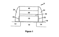
ゲート構造は、トランジスタの一素子である。図1は、ゲートスタック8の例を示している。半導体の基板10は、基板(12,14)内のドープ領域(ソース・ドレン領域)に重なるゲートの絶縁層16を支持し、ゲート絶縁層は、典型的には多結晶シリコンであるゲート18を支持する。ゲート上には金属層30がある。金属層は、全体的にバリヤー層20として示される窒化物、酸化物又はケイ素化合物のような、1つ又はそれ以上の他の層によりゲートから分離される。次いで、金属層は、窒化物、酸化物又はケイ素化合物のような1つ又はそれ以上の他の層(全体を40)を支持する。酸化物22が、ゲートスタックの根元部においてゲート酸化物を保護するために、ゲートの側面に形成され、そして絶縁スペーサー24が、ゲートスタックのいずれかの側面に形成される。更に、基板内のソース・ドレン領域に対するコンタクト及びゲート構造に対するコンタクトが形成されることがある。
The gate structure is one element of a transistor. FIG. 1 shows an example of the gate stack 8. The semiconductor substrate 10 supports a gate insulating layer 16 overlying a doped region (source / drain region) in the substrate (12, 14), and the gate insulating layer includes a
自己整合コンタクト(self‐aligned contact=SAC)は、ゲートと基板へのバイアコンタクトとの間の距離を、最大で最小ゲート幅の2分の1にするような半導体素子の設計を可能にする。典型的には、SACは、整合不良のコンタクトがゲート自体に接触することを阻止するために窒化物を含むようにされたスペーサーと共に、ゲートスタック上の窒化層を使用する。窒化物が存在していない場合には、コンタクトとなる穴を形成するために使用されるエッチングが、誘電体層を貫通してゲートに達することになる。窒化物が存在する場合には、窒化層とスペーサーは、エッチングのストップ作用を果たし、不整合のために穴がゲートまで達するようになることを防止し、したがって、コンタクトとゲートの間に遥かに小さな平均距離を持つ素子設計を可能にする。 The self-aligned contact (self-aligned contact = SAC) enables the design of semiconductor devices such that the distance between the gate and the via contact to the substrate is at most one-half of the minimum gate width. Typically, a SAC uses a nitride layer on the gate stack with a spacer that is adapted to include nitride to prevent misaligned contacts from contacting the gate itself. In the absence of nitride, the etch used to form the contact hole will penetrate the dielectric layer to the gate. In the presence of nitride, the nitride layer and spacer serve as an etch stop, preventing the holes from reaching the gate due to misalignment, and thus far between the contact and gate. Enables device design with a small average distance.
ゲートスタック上の窒化層は、SACの形成に使用されるときには少なくとも800オングストロームの厚さがある。エッチング停止層又はハードマスクのような他の目的にのみ使用される場合には、800オングストローム以下の厚さが使用される。また、少なくとも800オングストロームの厚さは、誘電体層が形成された後の厚さであり、窒化層は、最初に形成されたときには通常はもっと厚く、ゲートエッチングの間に約500オングストロームの損失を許容し(例えばハードマスク機能としての厚さ)、窒化物スペーサーの形成の間に約200オングストロームの損失を許容する。 The nitride layer on the gate stack is at least 800 angstroms thick when used to form a SAC. If used only for other purposes such as an etch stop layer or hard mask, a thickness of 800 angstroms or less is used. Also, the thickness of at least 800 Angstroms is the thickness after the dielectric layer is formed, and the nitride layer is usually thicker when first formed, resulting in a loss of about 500 Angstroms during gate etching. Allow (eg, thickness as a hard mask function) and allow a loss of about 200 angstroms during nitride spacer formation.
集積回路及び半導体構造体内の素子の大きさを減らすことについて継続する必要性がある。素子の大きさが減少するにつれて、望ましいより小さな形状を得るためには、フォトレジストを露光するのに、より短い波長の放射線が必要である。このため、より短い波長の放射線に感度を持つフォトレジストを使用しなければならない。0.1ミクロンのオーダーの形状を得るために、193ナノメートルの波長を持つ放射線が使用されており、この波長に対して感度を持つフォトレジストは193ナノメートル・レジストと呼ばれる。このレジストは、T9269(スイス、ムッテン、Clariant International Ltd.製)、6A100(日本川崎市 東京応化工業株式会社)、及びAR414とAR237(両方とも日本、東京、日本合成ゴム株式会社製)のように種々のものが市販されている。 There is a continuing need to reduce the size of devices in integrated circuits and semiconductor structures. As the device size decreases, shorter wavelength radiation is required to expose the photoresist in order to obtain the desired smaller shape. For this reason, a photoresist sensitive to shorter wavelength radiation must be used. In order to obtain shapes on the order of 0.1 microns, radiation having a wavelength of 193 nanometers is used, and photoresists sensitive to this wavelength are called 193 nanometer resists. The resists are T9269 (Mutten, Switzerland, Clariant International Ltd.), 6A100 (Nippon Kawasaki City Tokyo Ohka Kogyo Co., Ltd.), and AR414 and AR237 (both from Japan, Tokyo, Nippon Synthetic Rubber Co., Ltd.). Various products are commercially available.
しかし、遭遇する好ましくない問題は、エッチング処理が特定のフォトレジストに対して最適化され、スケールの減少に伴って異なるフォトレジストに切り換えることにより、ラインエッジ粗さの増大のような問題を生じ得ることである。(「An Experimentally Validated Analytical Model For Gate Line‐Edge Roughness (LER) Effects on Technology Scaling」 Diaz, C. H.他 IEEE Electronic Device Letters,22巻No.6,287から89ページ(2001年6月)を参照のこと)。ラインエッジ粗さが増大すると素子の不良や素子の収益の減少という結果になる。 However, undesired problems encountered can cause problems such as increased line edge roughness by switching to a different photoresist as the etching process is optimized for a particular photoresist and scale decreases. That is. (“An Experientially Validated Analytical Model for Gate Line-Edge Roughness (LER) Effects on Technology Scaling,” Vol.6, E.E.E.E.E.E. See Increasing line edge roughness results in device failure and reduced device revenue.
第一の態様においては、本発明は、窒化層をプラズマによりエッチングして、パターン形成された窒化層を形成することを含む半導体構造体を製造する方法である。窒化層は半導体の基板上にあり、フォトレジスト層が窒化層上にあり、プラズマは、少なくとも10ミリトルの圧力においてCF4(テトラフルオルメタン)及びCHF3(トリフルオルメタン)を含むガス混合物から形成される。 In a first aspect, the present invention is a method of manufacturing a semiconductor structure that includes etching a nitride layer with plasma to form a patterned nitride layer. The nitride layer is on a semiconductor substrate, the photoresist layer is on the nitride layer, and the plasma is from a gas mixture comprising CF 4 (tetrafluoromethane) and CHF 3 (trifluoromethane) at a pressure of at least 10 millitorr. It is formed.
第二の態様においては、本発明は窒化層をプラズマによりエッチングして、パターン形成された窒化層を形成することを含む半導体構造体を製造する方法である。窒化層はスタック上にあり、スタックは半導体の基板上にあり、スタックは、(i)ケイ素を含むゲート層、及び(ii)ゲート層上の金属層を含んでいる。フォトレジスト層は窒化層上にあり、フォトレジスト層は193ナノメートルのフォトレジストを含み、パターン形成された窒化層は8ナノメートル以下のラインエッジ粗さであり、プラズマは炭素、水素及びフッ素から構成される。 In a second aspect, the present invention is a method of manufacturing a semiconductor structure comprising etching a nitride layer with plasma to form a patterned nitride layer. The nitride layer is on the stack, the stack is on a semiconductor substrate, and the stack includes (i) a gate layer comprising silicon, and (ii) a metal layer on the gate layer. The photoresist layer is on the nitride layer, the photoresist layer includes a 193 nanometer photoresist, the patterned nitride layer has a line edge roughness of 8 nanometers or less, and the plasma is from carbon, hydrogen and fluorine. Composed.
第三の態様においては、本発明は、半導体基板上のパターン形成された窒化層を含む半導体構造体である。パターン形成された窒化層は9ナノメートル以下のラインエッジ粗さであり、基板の分離領域は0.4ミクロン以下の幅である。 In a third aspect, the present invention is a semiconductor structure that includes a patterned nitride layer on a semiconductor substrate. The patterned nitride layer has a line edge roughness of 9 nanometers or less and the isolation region of the substrate is 0.4 microns or less in width.
ラインエッジ粗さは任意の線に沿って1ミクロン間隔で均一に取られた10個の重要寸法(critical demension=CD)の読み値の3シグマとして定義される。(「An Experimentally Validated Analytical Model For Gate Line‐Edge Roughness(LER) Effects on Technology Scaling」 Diaz, C. H.他 IEEE Electronic Device Letters,22巻No.6,287から89ページ(2001年6月)における長距離LERの説明を参照のこと) Line edge roughness is defined as 3 sigma of 10 critical dimension (CD) readings taken uniformly along the line at 1 micron intervals. (“An Experientially Validated Analytical Model For Gate Line-Edge Roughness (LER) Effects on Technology Scaling, Volumes 6 to 7 E.E.E.E.E.E.E.E. (See description of long distance LER)
本発明は、9ナノメートル以下のラインエッジ粗さを生成するための新規な窒化物エッチング方法の発見を利用している。一般的に、窒化物のエッチングは、エッチングが4ミリトルの圧力のもとでCH2F2(ジフルオルメタン)により形成されたプラズマで実行された場合、193ナノメートル・レジストに対して10から12ナノメートルのラインエッジ粗さという結果となる。9ナノメートル以下のラインエッジ粗さはエッチングのプラズマ圧力を著しく増加させること、及びプラズマにおけるフッ素濃度を増加させることにより達成される。 The present invention takes advantage of the discovery of a novel nitride etch method to produce line edge roughness below 9 nanometers. In general, nitride etching is performed from 10 for a 193 nanometer resist when the etching is performed with a plasma formed by CH 2 F 2 (difluoromethane) under a pressure of 4 millitorr. The result is a line edge roughness of 12 nanometers. Line edge roughness below 9 nanometers is achieved by significantly increasing the plasma pressure of the etch and increasing the fluorine concentration in the plasma.
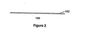
図2を参照すると、ゲート絶縁層102が半導体基板100上にある。半導体基板は、従来から知られている半導体材料とすることができる。半導体の例は、ケイ素、ガリウムヒ素、ゲルマニウム、窒化ガリウム、リン化アルミニウム、及び、0≦x≦1として、Si1‐xGex及びAIxGa1‐xAsのような合金を含む。半導体基板はケイ素が好ましく、ケイ素はドープされたものでも、されていないものでもよい。ゲート絶縁層102は、従来から知られている絶縁体材料とすることができる。例えば、ゲート絶縁層は、シリコン酸化物又はシリコン窒酸化物を含むことができる。
Referring to FIG. 2, the
図3を参照すると、ゲート層105がゲート絶縁層上に形成される。このゲート層は、様々な半導体材料を含むことができる。典型的には、ゲート層は、多結晶シリコン(ポリ)又はアモルファスシリコンを含む。ゲート層は、一つの型のドープ剤(P+又はN+)によりドープされるか、又は、区分された領域に両方の型のドープ剤を含むことができる。分割ゲートは、P+とN+両方のドーピング領域を持つゲート層である。
Referring to FIG. 3, a
分割ゲートの場合、P+型ドープされた(B又はBF2 +で)ゲート領域が基板のN-型ドープされたチャンネル領域上にあってPMOS(P型金属酸化膜半導体)素子を形成し、N+型ドープされた(As+又はリン+で)ゲート領域が、基板のP-型ドープされたチャンネル領域上にあってNMOS(N型金属酸化膜半導体)素子を形成する。ゲートのP+及びN+ドーピング領域は、基板の分離領域上にある領域で分離されており、この分離領域の幅は0.4ミクロン以下、より好ましい幅は0.36ミクロン以下である。ゲート領域のドーピングは、ゲートの形成後に、各領域を別々にマスキング及びドーピングするか、或いは一つの型のドープ剤でゲート全体をドーピンし、次いで他の型のドープ剤で一つの領域だけをマスキング及びドーピングする(カウンタードーピング処理)ことにより遂行することが好ましい。 In the case of a split gate, a P + -type doped (in B or BF 2 + ) gate region is on the N − -type doped channel region of the substrate to form a PMOS (P-type metal oxide semiconductor) device; An N + -doped (as + or phosphorous + ) gate region is on the P − -doped channel region of the substrate to form an NMOS (N-type metal oxide semiconductor) device. The P + and N + doping regions of the gate are separated by a region on the isolation region of the substrate, the isolation region having a width of 0.4 microns or less, more preferably 0.36 microns or less. Gate region doping can be done by masking and doping each region separately after gate formation, or by doping the entire gate with one type of dopant and then masking only one region with another type of dopant. And it is preferable to carry out by doping (counter doping treatment).
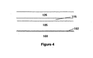
図4を参照すると、任意にバリヤー層115をゲート層上に形成することができる。この任意のバリヤー層は、窒化物、ケイ素化合物、酸化物を含む様々な物質を含むことができ、導電性材料が好ましい。例えば、バリヤー層は、耐火ケイ素化合物及び窒化物を含むことができる。バリヤー層は、窒化ケイ素、或いは、タンタル、チタニウム、ニオブ又はタングステンのような金属の窒化物又はケイ化物、例えば窒化タングステンを含むことが好ましい。
Referring to FIG. 4, a
更に図4を参照すると、金属層125が存在させる場合には、該金属層125は、ゲート層上又はバリヤー層115上に形成することができる。金属層の厚みは200から600オングストロームが好ましく、更に好ましいのは300から500オングストロームであり、325から450オングストロームが最も好ましい。金属層125は、様々な金属含有物質を含むことができる。例えば、金属層は、アルミニウム、銅、タンタル、チタニウム、タングステン、或いはその合金又は化合物を含むことができる。金属層はタングステン又はチタニウムからなることが好ましい。例えば、金属層は、金属の物理的気相成長法(PVD)又はハロゲン化金属と水素の混合物の低圧化学蒸着法(LPCVD)によって形成することができる。
Still referring to FIG. 4, if a
図5を参照すると、任意にバリヤー層135を金属層上に形成することができる。この第2の任意のバリヤー層の形成は、第1の任意のバリヤー層115について説明したように遂行することができ、この層は、同じ物質により同じ厚さに形成することができる。
Referring to FIG. 5, a
更に図5を参照すると、エッチング停止層145が、化学蒸着法(CVD)を含む様々な方法で金属層上に形成される。エッチング停止層は、窒化層であることが好ましい。更には、エッチング停止層は、プラズマ増強化学蒸着法(PECVD)により形成された窒化ケイ素であることが好ましい。エッチング停止層は、組成を異ならせ、エッチング停止層の上に反射防止があるように、例えばエッチング停止層の上にケイ素濃度の高い窒化ケイ素、又はケイ素の酸窒化物があるようにし、この層が後のエッチング中にエッチング停止層を保護するハードマスクの機能も果たすようにすることができる。代わりに、別の反射防止層(ARC)を形成することができる。
Still referring to FIG. 5, an
エッチング停止層は、比較的低温で急速に形成することが好ましい。例えば、ゲート層がP+及びN+両方のドーピング領域を含む場合には、ウェハが十分に高温のもとで長時間保持されるとドープ剤の拡散を生じる。したがって、どんな高温処理も、比較的短時間においてのみ行われることが望ましい。同様に、長時間の処理はいずれも、比較的低温で行われることが望ましい。もし大気が実質的に無酸素であれば、或いは還元環境(水素を多く含む)であれば、エッチング停止層は、750度までの温度のもとで形成されることが好ましい。典型的な状況のもとでは、600度までの温度が好ましく、450度までが更に好ましい。少なくとも350度の温度、例えば400度が好ましい。エッチング停止層の被着は、分割ゲートにおけるP+領域とN+領域の間で実質的な拡散を生じない温度及び時間で遂行されることが好ましい。 The etch stop layer is preferably formed rapidly at a relatively low temperature. For example, if the gate layer includes both P + and N + doped regions, dopant diffusion occurs when the wafer is held at a sufficiently high temperature for an extended period of time. Therefore, it is desirable that any high temperature treatment be performed only in a relatively short time. Similarly, it is desirable that any long-time treatment be performed at a relatively low temperature. If the atmosphere is substantially oxygen-free or if it is a reducing environment (containing a lot of hydrogen), the etch stop layer is preferably formed at a temperature of up to 750 degrees. Under typical circumstances, temperatures up to 600 degrees are preferred, and up to 450 degrees are more preferred. A temperature of at least 350 degrees, for example 400 degrees, is preferred. The deposition of the etch stop layer is preferably performed at a temperature and time that does not cause substantial diffusion between the P + and N + regions in the split gate.
エッチング停止層は、ゲート層のエッチングの後で、かつ、ゲートスペーサーの形成の後の状態で、少なくとも800オングストロームの厚さが好ましく、少なくとも1100オングストロームが一層好ましく、最も好ましいのは少なくとも1200オングストロームである。エッチング停止層の約500オングストロームがゲート層のエッチング中に失われ、エッチング停止層の約200オングストロームがスペーサーの形成の間に失われる。少なくとも1500オングストロームの厚さにエッチング停止層を被着させることが好ましく、少なくとも1800オングストロームの厚さにエッチング停止層を被着させることが一層好ましく、少なくとも2100オングストロームの厚さにエッチング停止層を被着させることが最も好ましい。ゲート層のエッチングの後で、かつ、ゲートスペーサーの形成の後(或いはその代わりとして誘電体層が形成された後)の状態で、エッチング停止層は800から1800オングストロームの厚さが好ましく、1100から1500オングストロームの厚さが一層好ましく、最も好ましいのは1200から1400オングストロームである。同様に、工程におけるゲート層エッチング及びスペーサー形成の各点においてエッチング停止層の損失を生じるような物質が使われるときには、成層付着される厚みは、上述と同様の範囲に、ゲート層のエッチング及びスペーサーの形成の間に生じる損失を調整するための追加の700オングストロームを付加したものとすることが好ましい。 The etch stop layer is preferably at least 800 angstroms thick, more preferably at least 1100 angstroms, most preferably at least 1200 angstroms after etching the gate layer and after formation of the gate spacer. . About 500 Å of the etch stop layer is lost during the etching of the gate layer, and about 200 Å of the etch stop layer is lost during the formation of the spacer. Preferably, the etch stop layer is deposited to a thickness of at least 1500 angstroms, more preferably the etch stop layer is deposited to a thickness of at least 1800 angstroms, and the etch stop layer is deposited to a thickness of at least 2100 angstroms. Most preferably. Preferably after etching the gate layer and after forming the gate spacer (or after the dielectric layer is formed), the etch stop layer is preferably between 800 and 1800 angstroms thick. A thickness of 1500 angstroms is more preferred and most preferred is 1200 to 1400 angstroms. Similarly, when a material that causes loss of the etch stop layer at each point of gate layer etching and spacer formation in the process is used, the thickness of the deposited layer is within the same range as described above, and the gate layer etching and spacer It is preferable to add an additional 700 angstroms to adjust for the losses that occur during the formation of.
図6−9を参照すると、各層は、ゲートスタックを形成するためにパターン形成することができる。このパターン形成は、例えば従来の写真平版技術とエッチング技術により遂行することができる。図6及び7を参照すると、例えば、エッチング停止層145(図6)上にパターン状のフォトレジスト210を形成し、次いで層の露光された部分をエッチングすることによってエッチングを行い、パターン形成されたエッチング停止層150を形成することによって、エッチング停止層が形成される。側壁の不動態化状態を除くために、フッ化水素酸浸漬を使用することができる。
Referring to FIGS. 6-9, each layer can be patterned to form a gate stack. This pattern formation can be performed by, for example, conventional photolithography and etching techniques. Referring to FIGS. 6 and 7, for example, a
エッチング停止層のエッチングは、ガス混合物から形成されたプラズマに露出することにより遂行することができる。ガス及びプラズマは、炭素、フッ素及び水素から構成することが好ましい。フッ素と水素の原子比は、43:1から13:3が好ましく、35:1から5:1が更に好ましく、27:1から7:1が最も好ましい。ガス混合物は、CF4及びCHF3を含むことが好ましく、CF4とCHF3の容積比は、10:1から1:3が好ましく、8:1から1:2が更に好ましく、6:1から1:1が最も好ましい。ガス混合物及びプラズマは又、He(ヘリウム)、Ne(ネオン)又はAr(アルゴン)のような他のガスを含むことができる。エッチング中の圧力は、4ミリトルより大きく、10から80ミリトルのように、少なくとも10ミリトルが好ましく、15から45ミリトルのように、少なくとも15ミリトルが更に好ましく、25から35ミリトルが最も好ましい。 Etching the etch stop layer can be accomplished by exposure to a plasma formed from a gas mixture. The gas and plasma are preferably composed of carbon, fluorine and hydrogen. The atomic ratio of fluorine to hydrogen is preferably 43: 1 to 13: 3, more preferably 35: 1 to 5: 1, and most preferably 27: 1 to 7: 1. Gas mixture preferably comprises CF 4 and CHF 3, the volume ratio of CF 4 and CHF 3 is 10: 1 to 1: 3 are preferred, 8: 1 to 1: 2 more preferably, 6: 1 1: 1 is most preferred. The gas mixture and plasma can also include other gases such as He (helium), Ne (neon) or Ar (argon). The pressure during etching is greater than 4 millitorr, preferably at least 10 millitorr, such as 10 to 80 millitorr, more preferably at least 15 millitorr, such as 15 to 45 millitorr, most preferably 25 to 35 millitorr.
到達したラインエッジ粗さは9ナノメートル以下、好ましくは8ナノメートル以下、6ナノメートル以下となることが最も好ましい。このプラズマエッチングのその他の利点は、フォトレジストの消費が少ないことである。このプラズマエッチングは、窒化層を形成する他のステップにおいて、例えば、浅いトレンチ分離(STI)形成工程中といった、分離領域の形成中に使用することができる。 The reached line edge roughness is most preferably 9 nanometers or less, preferably 8 nanometers or less, or 6 nanometers or less. Another advantage of this plasma etching is that it consumes less photoresist. This plasma etching can be used in other steps of forming the nitride layer, eg, during the formation of the isolation region, such as during a shallow trench isolation (STI) formation process.
図8を参照すると、パターン状のエッチング停止層は、パターン状の金属層130を形成するために金属層125(図7)をエッチングする場合のハードマスクとして使用することができる。図9を参照すると、パターン状のエッチング停止層とパターン状の金属層は、パターン状のゲート層110を形成するためにゲート層105(図8)をエッチングする場合のハードマスクとして使用することができる。ゲートのエッチングは、例えば塩素、臭化水素酸及び/又は酸素から形成されたプラズマに露出することによる従来のゲートエッチング技術によって遂行することができる。
Referring to FIG. 8, the patterned etch stop layer can be used as a hard mask when etching the metal layer 125 (FIG. 7) to form the patterned metal layer. Referring to FIG. 9, the patterned etch stop layer and the patterned metal layer may be used as a hard mask when etching the gate layer 105 (FIG. 8) to form the patterned
パターン形成されたフォトレジスト210(図6)は、エッチング停止層のエッチングに続くゲートスタック形成のいずれかのステップにおいて除去できる。例えば、パターン形成されたフォトレジストは、エッチング停止層のエッチング(図6と7に示されるように)直後に除去できるし、或いは金属層のエッチングの後又はゲートエッチングの後で除去できる。フォトレジストの除去に続いて、フォトレジストの残留副産物の除去又はフォトレジストの除去を確認するための洗浄手順を行うことができる。例えば、フォトレジストは、パターン形成されたフォトレジストをアッシングしてパターン形成されたエッチング停止層(図を有するゲートスタックを構成することにより除去することができる。フォトレジスト層のないこのゲートスタックは、次いで洗浄液で処理して、洗浄工程と除去を完了することができる。最も好ましい洗浄剤は、水、2−(2アミノエチレン)エタノール、ヒドロキシルアミン、及びカテコールを含むものである。洗浄液の例としては、EKC265(カリフォルニア州へーワード、EKC)がある。 The patterned photoresist 210 (FIG. 6) can be removed at any step of gate stack formation following etching of the etch stop layer. For example, the patterned photoresist can be removed immediately after etching the etch stop layer (as shown in FIGS. 6 and 7) or can be removed after etching the metal layer or after gate etching. Following removal of the photoresist, a cleaning procedure can be performed to confirm removal of residual photoresist by-products or removal of the photoresist. For example, the photoresist can be removed by ashing the patterned photoresist to form a patterned etch stop layer (a gate stack having a figure. This gate stack without the photoresist layer is It can then be treated with a washing solution to complete the washing step and removal, the most preferred washing agent comprising water, 2- (2aminoethylene) ethanol, hydroxylamine, and catechol. EKC265 (Heward, CA, EKC).
このように、図9は、半導体のウェハ上に形成できるゲートスタック200を表している。半導体の基板100はゲート絶縁層102を支持し、該ゲート絶縁層102は順にゲート層110を支持している。ゲート層は金属層130を支持し、該金属層130は任意にバリヤー層120によりゲート層から分離することができる。任意に、金属層はバリヤー層140を支持するようにすることができる。エッチング停止層150は、金属層130上、或いは任意に該金属層の上方の層140の上にある。
9 illustrates a
ゲート構造の更なる処理は、ゲート層110上の側壁の酸化物領域170を形成することと、スタックの側面にスペーサー160(酸化物を含むことが好ましい)を形成することを含むことができる。更に、図10に示されるように、誘電体層180をエッチング停止層上に形成することができ、かつ、該誘電体を通って基板に達するようにコンタクト又はバイア190を形成することができる。このバイアは、例えばTiN及びタングステンのそれぞれにより線形成及び充填されてバイアコンタクトを形成することができる。他の処理は、ゲート自体に対するコンタクトの形成を含むことができる。誘電体層が形成された後に、エッチング停止層は、少なくとも800オングストローム、更に好ましくは少なくとも1100オングストロームの厚さであり、これは、SACの形成を可能にするために使用できる。
Further processing of the gate structure may include forming
該半導体構造体から半導体素子を形成することを完了するために、他の処理を使用することができる。例えば、ソース/ドレン領域12、14を基板内に形成することができ、追加の誘電体層を基板上に形成することができ、コンタクト及び金属化層をこれらの構造上に形成することができる。これらの追加の素子は、ゲートスタックの形成の前、形成中又はその後に形成することができる。
Other processes can be used to complete the formation of semiconductor elements from the semiconductor structure. For example, source /
本発明において使用するための、ゲートスタック層のエッチング、及び、研磨、洗浄、被着のステップのような他のステップを含む関連の処理ステップは、当技術における当業者によく知られており、Kirk‐Othmerによる工業化学百科事典の14巻、677から709ページ(1995年)、Semiconductor Device Fundamentals、Robert F. Pierret、Addison−Wesley、1996年、Wolf、Silicon Processing for the VLSI Era. Lattice Press、1986年、1990年、1995年(それぞれの1から3巻)、及び、Microship Fabrication 第4版、Peter Van Zant、Mcgraw−Hill、2000年において説明されている。 Related processing steps for use in the present invention, including gate stack layer etching and other steps such as polishing, cleaning, deposition steps, are well known to those skilled in the art, Kirk-Othmer, Encyclopedia of Industrial Chemistry, Vol. 14, 677-709 (1995), Semiconductor Device Fundamentals, Robert F. Pierret, Addison-Wesley, 1996, Wolf, Silicon Processing for the VLSI Era. Lattice Press, 1986, 1990, 1995 (1 to 3 volumes each), and Microsoft Fabric Fabrication 4th Edition, Peter Van Zant, Mcgraw-Hill, 2000.
本発明の半導体構造体は、例えばSRAM、DRAM、EPROM、EEPROMなどのようなメモリーセル、プログラム可能論理装置、データ通信装置、クロック発振装置などの集積回路のような半導体素子に組み込むことができる。更に、この半導体素子のいずれも、例えばコンピュータ、航空機又は自動車のような電子素子に組み込まれる。 The semiconductor structure of the present invention can be incorporated into a semiconductor element such as an integrated circuit such as a memory cell such as SRAM, DRAM, EPROM, or EEPROM, a programmable logic device, a data communication device, or a clock oscillation device. In addition, any of these semiconductor elements can be incorporated into electronic elements such as computers, aircraft or automobiles.
実施例1−ゲート構造の形成
以下の詳細なステップが、分割ゲートを有するゲートスタックを形成するために使用された。
Example 1-Formation of Gate Structure The following detailed steps were used to form a gate stack with split gates.

底部反射防止膜(BARC)が、以下の条件でエッチングされた。CF4流量100sccm(標準立方センチメートル/毎分)、Ar流量100sccm、電力600W、バイアス75W、圧力16ミリトル、温度60度。温度は、BARCエッチング中並びにその後のステップにおいて、例えばHe背後冷却により制御される。
The bottom antireflection film (BARC) was etched under the following conditions. CF 4 flow rate 100 sccm (standard cubic centimeter / min),
次いで、レジストは、HBr(臭化水素)流量160sccm、O2流量28sccm、電力400W、圧力8ミリトル、温度60度、10秒間という条件下でトリムされた。代替的に、レジストは、以下の条件でトリムされた。HBr流量169sccm、O2流量19sccm、電力400W、圧力8ミリトル、温度60度、5秒間。
The resist was then trimmed under conditions of HBr (hydrogen bromide)
窒化物のエッチングは、プラズマにより、圧力30ミリトル、電力500W、バイアス100W、温度60から65度という条件下で遂行された。ガス組成は、275sccmでのCHF3と、300sccmでのCF4である。20%のオーバーエッチングが使用された。 Nitride etching was performed by plasma under conditions of a pressure of 30 mTorr, a power of 500 W, a bias of 100 W, and a temperature of 60 to 65 degrees. The gas composition is CHF 3 at 275 sccm and CF 4 at 300 sccm. A 20% overetch was used.
タングステンは、NF3(三フッ化窒素)流量10sccm、Cl2流量25sccm、O2流量5sccm、Ar流量50sccm、N2流量30sccm、He流量150sccm、電力800W,バイアス60W、圧力4ミリトル、温度60度、10秒間の条件下でエッチングされた。
Tungsten is NF 3 (nitrogen trifluoride) flow rate 10 sccm, Cl 2 flow rate 25 sccm, O 2 flow rate 5 sccm, Ar flow rate 50 sccm, N 2 flow rate 30 sccm, He flow
レジスト材料は、アッシング(例えば、80度においてCF4及びO2混合物のもとでの)により除去され、スタックは、EKC265(カリフォルニア州へーワード、EKC、2−(2アミノエチレン)エタノール、ヒドロキシルアミンとカテコールの混合)を用いて65又は70度において10分間、そして20度において2分間噴霧しながら(噴霧用ツールを使用)回転させることによりウェハを処理し、それに続いて、タングステンの望ましくない酸化を防ぐために、脱イオン水によるリンス行うことによって洗浄された。この洗浄は、望ましくない酸化を防ぐために、タングステン又はタングステン窒化物が遭遇するあらゆる除去ステップ及び洗浄ステップにも使用される。また、以下の条件により洗浄を行って、その後で、水洗浄を行い、下流側においてプラズマアッシングを行うこともできる。〔ステップ1〕CF4流量50sccm、H2O流量160sccm、N2/H2流量1400sccm、電力1050W、バイアス100W、圧力750ミリトル、温度80度、30秒間。〔ステップ2〕NF3流量40sccm、H2O流量170sccm、O2流量170sccm、バイアス150W、250ミリトルの圧力、温度80度、120秒間。
The resist material is removed by ashing (eg, under a CF 4 and O 2 mixture at 80 degrees) and the stack is EKC265 (Heward, CA, EKC, 2- (2 aminoethylene) ethanol, hydroxylamine And catechol) to treat wafers by spinning (using a spraying tool) at 65 or 70 degrees for 10 minutes and at 20 degrees for 2 minutes followed by undesirable oxidation of tungsten In order to prevent this, it was washed by rinsing with deionized water. This cleaning is also used for any removal and cleaning steps encountered by tungsten or tungsten nitride to prevent unwanted oxidation. In addition, cleaning can be performed under the following conditions, followed by water cleaning, and plasma ashing can be performed on the downstream side. [Step 1] CF 4 flow rate 50 sccm, H 2
次いで、タングステンは、以下の条件、すなわち、NF3流量15sccm、Cl2流量25sccm、O2流量5sccm標準立方センチメートル毎分、Ar流量50sccm、N2流量30sccm、He流量150sccm、電力800W、バイアス35W、圧力4ミリトル、温度60度という条件下でエッチングされた。タングステンのオーバーエッチングが5秒間実行された。その時システムは20秒間にわたりポンプダウンされた。
Tungsten then has the following conditions: NF 3 flow rate 15 sccm, Cl 2 flow rate 25 sccm, O 2 flow rate 5 sccm standard cubic centimeter per minute, Ar flow rate 50 sccm, N 2 flow rate 30 sccm, He flow
次いで、ポリは、HBr流量250sccm、He(80%)/O2(20%)流量12sccm、電力450W、バイアス40W、圧力25ミリトル、温度60度という条件のもとでエッチングされた。ポリのオーバーエッチングは、HBr流量150sccm、He(80%)/O2(20%)流量8sccm、He流量100sccm、電力200W、バイアス70W、圧力70ミリトル、温度60度、63秒間という条件のもとで遂行された。代わりに、ポリのオーバーエッチングは、HBr流量150sccm、He(80%)/O2(20%)流量13sccm、He流量200sccm、電力250W、バイアス60W、圧力80ミリトル、温度60度、53秒間という条件のもとで遂行された。洗浄は上記のように行うことができ、或いは、例えば、以下の条件、すなわち、CF4流量40sccm、O2流量1000sccm、H2O流量200sccm、N2流量150sccm、電力1700W、圧力700ミリトル、温度70度、80秒間という条件のもとで洗浄を行い、その後で、下流側において水リンス(例えば脱イオン水で7サイクルにより)することにより遂行することができる。
The poly was then etched under the following conditions: HBr flow rate 250 sccm, He (80%) / O 2 (20%)
ポリの露出された側は、選択的酸化による約50から70オングストロームの厚さの酸化物の層で覆われていた。この工程は、タングステン及びタングステン窒化物とは異なり、ポリを選択的に酸化するために、温度750度のもとで、水素及び酸素(10%は蒸気)の混合物にスタックを曝すことにより遂行された。 The exposed side of the poly was covered with a layer of oxide approximately 50 to 70 angstroms thick by selective oxidation. This process, unlike tungsten and tungsten nitride, is accomplished by exposing the stack to a mixture of hydrogen and oxygen (10% steam) at a temperature of 750 degrees to selectively oxidize poly. It was.
スペーサー形成のための窒化層を形成するために、BTBASを以下の条件、すなわち、BTBAS流量50sccm、NH3流量100sccm、圧力150ミリトル、温度550度という条件のもとで使用した。
In order to form a nitride layer for spacer formation, BTBAS was used under the following conditions: BTBAS flow rate 50 sccm, NH 3 flow rate 100 sccm,
窒化物のエッチング(窒化物−ポリ切り出しマスクエッチング及び洗浄)は、圧力35ミリトル、電力280W、温度15度のもとで、プラズマにより実行された。主エッチングのガス組成は、30sccmのCHF3、60sccmのAr、10sccmのO2であった。洗浄は、次の2つのステップに基づきプラズマアッシングを使用して行い、その後で洗剤による洗浄を行った。
ステップ1:
圧力2ミリトル、温度185度、マイクロ波電力800W、ガスは、3750sccmのO2及び375sccmのN2。
ステップ2:
温度200度、マイクロ波電力1400Wであること以外は同じ値。
Nitride etching (nitride-poly cut mask etching and cleaning) was performed with plasma under a pressure of 35 mTorr, power of 280 W, and temperature of 15 degrees. The main etching gas composition was 30 sccm CHF 3 , 60 sccm Ar, 10 sccm O 2 . Cleaning was performed using plasma ashing based on the following two steps, followed by cleaning with a detergent.
Step 1:
Pressure 2 mTorr, Temperature 185 degrees, Microwave power 800 W, Gas is 3750 sccm O 2 and 375 sccm N 2 .
Step 2:
The same value except that the temperature is 200 degrees and the microwave power is 1400W.
コンタクトを形成するためのエッチング(SACエッチング)は、ARCエッチングの条件として、圧力55ミリトル、電力500W、温度35度、20ガウスの磁石、ガスは、5sccmのCF4、10sccmのCHF3、及び10sccmのC2H2F4におけるプラズマを使用し、主エッチングの条件は、55ミリトルの圧力、電力500W、温度35度、25ガウスの磁石、ガスは、80sccmのCHF3、8sccmのC2H2F4、90sccmのArであった。洗浄は、次の2つのステップによるプラズマでアッシングの後で、洗剤による洗浄を行うことにより遂行された。
ステップ1:
圧力400ミリトル、温度20±5度、RF電力420W、400sccmのO2ガス。
ステップ2:
圧力750ミリトル、温度20±5度、RF電力420W、ガスは、400sccmのN2、400sccmのH2、5sccmのNF3、或いは、その代わりとして、
圧力750ミリトル、温度40±5度、RF電力350W、ガスは、20sccmのCF4、200sccmのN2/5%H2、500sccmのO2。
Etching for forming a contact (SAC etching) is performed under the conditions of ARC etching, including a pressure of 55 mtorr, power of 500 W, temperature of 35 degrees, 20 gauss magnet, gas of 5 sccm of CF 4 , 10 sccm of CHF 3 , and 10 sccm. 's C 2 H 2 using a plasma in F 4, the main etching conditions, the pressure of 55 mTorr, power 500 W, temperature 35 degrees, 25 gauss magnets, gas, CHF 3 of 80 sccm, 8 sccm C 2 H 2 of F 4 , 90 sccm Ar. The cleaning was performed by ashing with a plasma according to the following two steps followed by cleaning with a detergent.
Step 1:
O 2 gas having a pressure of 400 mtorr, a temperature of 20 ± 5 degrees, an RF power of 420 W, and 400 sccm.
Step 2:
Pressure 750 mTorr,
Pressure 750 mtorr,
SACエッチング洗浄は、噴霧ツールによりEKC265を使用して、温度70度で10分間、更に20度で2分間行い、その後で、脱イオン水によるリンスを行い、次いで、N2内で回転乾燥をし、その後で、150度のH2SO4(硫酸)によりそれぞれ10分間ずつ2回洗浄し、N2内で回転乾燥をした。 The SAC etching cleaning is performed using EKC265 with a spray tool at a temperature of 70 ° C. for 10 minutes and then at 20 ° C. for 2 minutes, followed by rinsing with deionized water, followed by spin drying in N 2 . Then, each was washed twice for 10 minutes each with 150 degree H 2 SO 4 (sulfuric acid), and spin-dried in N 2 .
スタックにおいては、窒化ケイ素層は1300オングストロームの厚さであり(窒化ケイ素はポリエッチング及びスペーサーエッチングの間に失われるので被着した実際の量はより大きいのであるが)、タングステン層は325オングストロームの厚さであり、タングステン窒化層は75オングストロームの厚さであり、ポリ層は735オングストロームの厚さであった。コンタクトは、最上部では0.13ミクロンの幅であり、底部は0.05ミクロンの幅であった。 In the stack, the silicon nitride layer is 1300 angstroms thick (although the actual amount deposited is larger because silicon nitride is lost during the poly etch and spacer etch) and the tungsten layer is 325 angstroms thick. The tungsten nitride layer was 75 angstroms thick and the poly layer was 735 angstroms thick. The contacts were 0.13 microns wide at the top and 0.05 microns wide at the bottom.
Claims (20)
窒化層をプラズマによりエッチングして、パターン形成された窒化層を形成する工程を含み、
前記窒化層は半導体基板上にあり、
フォトレジスト層が前記窒化層上にあり、
前記プラズマは少なくとも10ミリトルの圧力においてCF4及びCHF3を含むガス混合物から調製される、
ことを特徴とする、前記方法。 A method for manufacturing a semiconductor structure, comprising:
Etching the nitride layer with plasma to form a patterned nitride layer;
The nitride layer is on a semiconductor substrate;
A photoresist layer is on the nitride layer;
The plasma is prepared from a gas mixture comprising CF 4 and CHF 3 at a pressure of at least 10 millitorr;
And said method.
前記圧力は25から35ミリトルであり、
前記フォトレジスト層は193ナノメートルのフォトレジストを含む、
ことを特徴とする請求項1に記載の方法。 The gas mixture has a CF 4 : CHF 3 ratio of 8: 1 to 1: 2.
The pressure is 25 to 35 millitorr;
The photoresist layer comprises a 193 nanometer photoresist;
The method according to claim 1.
窒化層をプラズマによりエッチングして、パターン形成された窒化層を形成する工程を含み、
前記窒化層はスタック上にあり、
前記スタックは半導体基板上にあり、
前記スタックは、
(i)ケイ素を含むゲート層と、
(ii)前記ゲート層上の金属層と、
を含み、
フォトレジスト層が前記窒化層上にあり、
前記フォトレジスト層は193ナノメートルのフォトレジストを含み、
前記パターン形成された窒化層は8ナノメートル以下のラインエッジ粗さを有し、
前記プラズマは炭素、水素及びフッ素を含む、
ことを特徴とする前記方法。 A method for manufacturing a semiconductor structure, comprising:
Etching the nitride layer with plasma to form a patterned nitride layer;
The nitride layer is on the stack;
The stack is on a semiconductor substrate;
The stack is
(I) a gate layer comprising silicon;
(Ii) a metal layer on the gate layer;
Including
A photoresist layer is on the nitride layer;
The photoresist layer comprises a 193 nanometer photoresist;
The patterned nitride layer has a line edge roughness of 8 nanometers or less;
The plasma includes carbon, hydrogen and fluorine;
Said method.
前記P+領域及びN+領域は、0.4ミクロン以下の幅を有する前記基板の分離領域上の領域により分離されている、
ことを特徴とする請求項7に記載の方法。 The gate layer includes a P + region and an N + region;
The P + region and the N + region are separated by a region on the separation region of the substrate having a width of 0.4 microns or less;
The method according to claim 7.
前記半導体構造体から半導体素子を形成する、
ことを特徴とする半導体素子を製造する方法。 Forming a semiconductor structure by the method of claim 1;
Forming a semiconductor element from the semiconductor structure;
A method for manufacturing a semiconductor device.
前記半導体素子を有する電子素子を形成する、
ことを特徴とする電子素子を製造する方法。 Forming a semiconductor element by the method of claim 12;
Forming an electronic element having the semiconductor element;
A method for manufacturing an electronic device.
前記半導体構造体から半導体素子を形成する、
ことを特徴とする半導体素子を製造する方法。 Forming a semiconductor structure by the method of claim 7;
Forming a semiconductor element from the semiconductor structure;
A method for manufacturing a semiconductor device.
前記半導体素子を有する電子素子を形成する、
ことを特徴とする電子素子を製造する方法。 Forming a semiconductor element by the method of claim 14;
Forming an electronic element having the semiconductor element;
A method for manufacturing an electronic device.
前記パターン形成された窒化層は、9ナノメートル以下のラインエッジ粗さであり、
前記基板の分離領域は、0.4ミクロン以下の幅を有する、
ことを特徴とする半導体構造体。 Including a patterned nitride layer on a semiconductor substrate;
The patterned nitride layer has a line edge roughness of 9 nanometers or less;
The isolation region of the substrate has a width of 0.4 microns or less;
A semiconductor structure characterized by that.
前記スタックは、
(i)ケイ素を含むゲート層と、
(ii)前記ゲート層上の金属層と、
を有し、
前記ゲート層は前記分離領域上にある、
ことを特徴とする請求項18に記載の半導体構造体。 A stack further between the nitride layer and the semiconductor structure;
The stack is
(I) a gate layer comprising silicon;
(Ii) a metal layer on the gate layer;
Have
The gate layer is on the isolation region;
The semiconductor structure according to claim 18.
Applications Claiming Priority (2)
| Application Number | Priority Date | Filing Date | Title |
|---|---|---|---|
| US10/314,380 US7229929B2 (en) | 2002-12-06 | 2002-12-06 | Multi-layer gate stack |
| PCT/US2003/038631 WO2004053936A2 (en) | 2002-12-06 | 2003-12-04 | Multi-layer gate stack |
Publications (2)
| Publication Number | Publication Date |
|---|---|
| JP2006509375A true JP2006509375A (en) | 2006-03-16 |
| JP2006509375A5 JP2006509375A5 (en) | 2007-01-25 |
Family
ID=32468458
Family Applications (1)
| Application Number | Title | Priority Date | Filing Date |
|---|---|---|---|
| JP2004559293A Pending JP2006509375A (en) | 2002-12-06 | 2003-12-04 | Multilayer gate stack |
Country Status (5)
| Country | Link |
|---|---|
| US (1) | US7229929B2 (en) |
| JP (1) | JP2006509375A (en) |
| KR (1) | KR20050085415A (en) |
| AU (1) | AU2003300819A1 (en) |
| WO (1) | WO2004053936A2 (en) |
Families Citing this family (14)
| Publication number | Priority date | Publication date | Assignee | Title |
|---|---|---|---|---|
| US7229929B2 (en) * | 2002-12-06 | 2007-06-12 | Cypress Semiconductor Corporation | Multi-layer gate stack |
| US20040217006A1 (en) * | 2003-03-18 | 2004-11-04 | Small Robert J. | Residue removers for electrohydrodynamic cleaning of semiconductors |
| US7371637B2 (en) * | 2003-09-26 | 2008-05-13 | Cypress Semiconductor Corporation | Oxide-nitride stack gate dielectric |
| US7153780B2 (en) * | 2004-03-24 | 2006-12-26 | Intel Corporation | Method and apparatus for self-aligned MOS patterning |
| US7351663B1 (en) * | 2004-06-25 | 2008-04-01 | Cypress Semiconductor Corporation | Removing whisker defects |
| KR100753138B1 (en) * | 2006-09-29 | 2007-08-30 | 주식회사 하이닉스반도체 | Method for fabricating semiconductor device |
| US8252640B1 (en) | 2006-11-02 | 2012-08-28 | Kapre Ravindra M | Polycrystalline silicon activation RTA |
| JP2008218867A (en) * | 2007-03-07 | 2008-09-18 | Elpida Memory Inc | Semiconductor device manufacturing method |
| US7951728B2 (en) * | 2007-09-24 | 2011-05-31 | Applied Materials, Inc. | Method of improving oxide growth rate of selective oxidation processes |
| US9406530B2 (en) | 2014-03-27 | 2016-08-02 | International Business Machines Corporation | Techniques for fabricating reduced-line-edge-roughness trenches for aspect ratio trapping |
| US10204960B2 (en) * | 2015-09-17 | 2019-02-12 | Taiwan Semiconductor Manufacturing Co., Ltd. | Method of forming polysilicon gate structure in image sensor device |
| US20170330764A1 (en) * | 2016-05-12 | 2017-11-16 | Lam Research Corporation | Methods and apparatuses for controlling transitions between continuous wave and pulsing plasmas |
| US10566211B2 (en) | 2016-08-30 | 2020-02-18 | Lam Research Corporation | Continuous and pulsed RF plasma for etching metals |
| US9865473B1 (en) * | 2016-11-15 | 2018-01-09 | Globalfoundries Inc. | Methods of forming semiconductor devices using semi-bidirectional patterning and islands |
Citations (3)
| Publication number | Priority date | Publication date | Assignee | Title |
|---|---|---|---|---|
| JP2001051424A (en) * | 1999-06-02 | 2001-02-23 | Semiconductor Leading Edge Technologies Inc | Fine pattern forming method |
| JP2002222868A (en) * | 2001-01-29 | 2002-08-09 | Fujitsu Ltd | Semiconductor device and its fabricating method |
| JP2006505141A (en) * | 2002-10-31 | 2006-02-09 | アプライド マテリアルズ インコーポレイテッド | Method for etching a silicon-containing dielectric material |
Family Cites Families (12)
| Publication number | Priority date | Publication date | Assignee | Title |
|---|---|---|---|---|
| TW320749B (en) * | 1994-09-22 | 1997-11-21 | Tokyo Electron Co Ltd | |
| US5817579A (en) * | 1997-04-09 | 1998-10-06 | Vanguard International Semiconductor Corporation | Two step plasma etch method for forming self aligned contact |
| JP3902835B2 (en) * | 1997-06-27 | 2007-04-11 | 東京応化工業株式会社 | Positive photoresist composition |
| US6635185B2 (en) * | 1997-12-31 | 2003-10-21 | Alliedsignal Inc. | Method of etching and cleaning using fluorinated carbonyl compounds |
| US6107135A (en) * | 1998-02-11 | 2000-08-22 | Kabushiki Kaisha Toshiba | Method of making a semiconductor memory device having a buried plate electrode |
| US6342452B1 (en) * | 1999-05-20 | 2002-01-29 | International Business Machines Corporation | Method of fabricating a Si3N4/polycide structure using a dielectric sacrificial layer as a mask |
| US6740566B2 (en) * | 1999-09-17 | 2004-05-25 | Advanced Micro Devices, Inc. | Ultra-thin resist shallow trench process using high selectivity nitride etch |
| US6258677B1 (en) * | 1999-10-01 | 2001-07-10 | Chartered Seminconductor Manufacturing Ltd. | Method of fabricating wedge isolation transistors |
| US6897120B2 (en) * | 2001-01-03 | 2005-05-24 | Micron Technology, Inc. | Method of forming integrated circuitry and method of forming shallow trench isolation in a semiconductor substrate |
| US6624068B2 (en) * | 2001-08-24 | 2003-09-23 | Texas Instruments Incorporated | Polysilicon processing using an anti-reflective dual layer hardmask for 193 nm lithography |
| US6451647B1 (en) * | 2002-03-18 | 2002-09-17 | Advanced Micro Devices, Inc. | Integrated plasma etch of gate and gate dielectric and low power plasma post gate etch removal of high-K residual |
| US7229929B2 (en) * | 2002-12-06 | 2007-06-12 | Cypress Semiconductor Corporation | Multi-layer gate stack |
-
2002
- 2002-12-06 US US10/314,380 patent/US7229929B2/en not_active Expired - Lifetime
-
2003
- 2003-12-04 WO PCT/US2003/038631 patent/WO2004053936A2/en active Application Filing
- 2003-12-04 JP JP2004559293A patent/JP2006509375A/en active Pending
- 2003-12-04 KR KR1020057010280A patent/KR20050085415A/en not_active Application Discontinuation
- 2003-12-04 AU AU2003300819A patent/AU2003300819A1/en not_active Abandoned
Patent Citations (3)
| Publication number | Priority date | Publication date | Assignee | Title |
|---|---|---|---|---|
| JP2001051424A (en) * | 1999-06-02 | 2001-02-23 | Semiconductor Leading Edge Technologies Inc | Fine pattern forming method |
| JP2002222868A (en) * | 2001-01-29 | 2002-08-09 | Fujitsu Ltd | Semiconductor device and its fabricating method |
| JP2006505141A (en) * | 2002-10-31 | 2006-02-09 | アプライド マテリアルズ インコーポレイテッド | Method for etching a silicon-containing dielectric material |
Also Published As
| Publication number | Publication date |
|---|---|
| US7229929B2 (en) | 2007-06-12 |
| US20040110387A1 (en) | 2004-06-10 |
| AU2003300819A8 (en) | 2004-06-30 |
| WO2004053936A2 (en) | 2004-06-24 |
| KR20050085415A (en) | 2005-08-29 |
| WO2004053936A3 (en) | 2005-03-17 |
| AU2003300819A1 (en) | 2004-06-30 |
Similar Documents
| Publication | Publication Date | Title |
|---|---|---|
| US7396773B1 (en) | Method for cleaning a gate stack | |
| US6667246B2 (en) | Wet-etching method and method for manufacturing semiconductor device | |
| US7256137B2 (en) | Method of forming contact plug on silicide structure | |
| JPH0621018A (en) | Dry etching method | |
| US5164331A (en) | Method of forming and etching titanium-tungsten interconnects | |
| US6878646B1 (en) | Method to control critical dimension of a hard masked pattern | |
| US7229929B2 (en) | Multi-layer gate stack | |
| KR100954107B1 (en) | Method for manufacturing semiconductor device | |
| US6586293B1 (en) | Semiconductor device and method of manufacturing the same | |
| US6943126B1 (en) | Deuterium incorporated nitride | |
| JP2004006902A (en) | Semiconductor device and its manufacturing method | |
| US8445381B2 (en) | Oxide-nitride stack gate dielectric | |
| US7189652B1 (en) | Selective oxidation of gate stack | |
| KR100616498B1 (en) | Fabricating method of semiconductor device with poly/tungsten gate electrode | |
| US6680516B1 (en) | Controlled thickness gate stack | |
| JP2003234325A (en) | Manufacturing method of semiconductor device | |
| CN111106158B (en) | Semiconductor structure and forming method thereof | |
| US6803321B1 (en) | Nitride spacer formation | |
| US6828187B1 (en) | Method for uniform reactive ion etching of dual pre-doped polysilicon regions | |
| JP4082280B2 (en) | Semiconductor device and manufacturing method thereof | |
| KR20060122578A (en) | Method for forming hard mask in semiconductor memory device | |
| KR100596899B1 (en) | Method for manufacturing semiconductor device | |
| US6555397B1 (en) | Dry isotropic removal of inorganic anti-reflective coating after poly gate etching | |
| US7256083B1 (en) | Nitride layer on a gate stack | |
| JP2008135765A (en) | Semiconductor device |
Legal Events
| Date | Code | Title | Description |
|---|---|---|---|
| A521 | Written amendment |
Free format text: JAPANESE INTERMEDIATE CODE: A523 Effective date: 20061121 |
|
| A621 | Written request for application examination |
Free format text: JAPANESE INTERMEDIATE CODE: A621 Effective date: 20061121 |
|
| A521 | Written amendment |
Free format text: JAPANESE INTERMEDIATE CODE: A821 Effective date: 20090526 |
|
| RD02 | Notification of acceptance of power of attorney |
Free format text: JAPANESE INTERMEDIATE CODE: A7422 Effective date: 20090526 |
|
| RD04 | Notification of resignation of power of attorney |
Free format text: JAPANESE INTERMEDIATE CODE: A7424 Effective date: 20090527 |
|
| A977 | Report on retrieval |
Free format text: JAPANESE INTERMEDIATE CODE: A971007 Effective date: 20091214 |
|
| A131 | Notification of reasons for refusal |
Free format text: JAPANESE INTERMEDIATE CODE: A131 Effective date: 20091222 |
|
| A02 | Decision of refusal |
Free format text: JAPANESE INTERMEDIATE CODE: A02 Effective date: 20100615 |