JP2006337997A - Display device - Google Patents
Display device Download PDFInfo
- Publication number
- JP2006337997A JP2006337997A JP2006126985A JP2006126985A JP2006337997A JP 2006337997 A JP2006337997 A JP 2006337997A JP 2006126985 A JP2006126985 A JP 2006126985A JP 2006126985 A JP2006126985 A JP 2006126985A JP 2006337997 A JP2006337997 A JP 2006337997A
- Authority
- JP
- Japan
- Prior art keywords
- display
- external light
- light intensity
- gradations
- gradation
- Prior art date
- Legal status (The legal status is an assumption and is not a legal conclusion. Google has not performed a legal analysis and makes no representation as to the accuracy of the status listed.)
- Withdrawn
Links
Images


Abstract
Description
本発明は、文字、静止画若しくは動画などを表示する画面を備えた表示装置に関するものであり、さまざまな使用環境下において、表示画面の視認性を改善するための技術に関する。 The present invention relates to a display device including a screen for displaying characters, still images, moving images, and the like, and relates to a technique for improving the visibility of the display screen under various usage environments.
携帯電話機をはじめとして、表示画面を液晶パネルで構成したさまざま電気製品が普及している。液晶パネルは薄型軽量といった特徴があり、ノート型と呼ばれるパーソナルコンピュータでは液晶パネルを備えたモバイル対応の製品が生産されている。また、PDA(Personal Digital Assistant)と呼ばれる情報端末も多数生産され普及しつつある。 Various electric products having a display screen composed of a liquid crystal panel, such as mobile phones, have become widespread. Liquid crystal panels are thin and light, and mobile computers with liquid crystal panels are being produced in personal computers called notebook computers. In addition, a large number of information terminals called PDA (Personal Digital Assistant) are being produced and spread.
液晶パネルに限らないが、この種の用途に用いられる表示用パネルは、見た目の画質が重要視されるようになり、明るさやコントラストを自動又は手動で調整する機能が備えられているものが多く普及している。例えば、液晶パネルのバックライトの輝度を上げずに、液晶の透過率を変化させて階調間視認性を高める調整機能を備えた液晶表示装置が知られている(特許文献1参照)。
しかしながら、液晶パネルは、300ルクスから700ルクスの室内環境下では良好な視認性を示すが、1,000ルクス以上の屋外環境下では視認性が著しく悪化してしまうという問題があった。反射型液晶パネルと呼ばれ、画素電極で外光を反射する構成にしたものあるが、屋内の蛍光灯下ではむしろ画質が低下してしまい、本質的な解決には至っていなかった。すなわち、暗所若しくは屋内の蛍光灯下から屋外の太陽光下まで広い範囲において視認性を確保することが解決されていなかった。 However, the liquid crystal panel has good visibility in an indoor environment of 300 lux to 700 lux, but has a problem that the visibility is significantly deteriorated in an outdoor environment of 1,000 lux or more. Although it is called a reflection type liquid crystal panel and has a configuration in which external light is reflected by the pixel electrode, the image quality is rather deteriorated under an indoor fluorescent lamp, so that an essential solution has not been achieved. That is, ensuring visibility in a wide range from a dark place or indoor fluorescent lamp to outdoor sunlight has not been solved.
そこで、本発明は、暗所から強い外光下においてもその表示が認識できる表示装置を提供することを目的とする。 In view of the above, an object of the present invention is to provide a display device that can recognize the display even under strong external light from a dark place.
本発明は、外光強度に応じて階調数を変化させて表示を行う表示装置である。すなわち、コントラスト比(例えば、白と黒)を50以上、好ましくは100以上を有する表示装置であって、外光強度が高いときには低階調の表示を行い、外光強度が低いときには高階調の表示を行い、外光強度が両者の間にあるときにはその中間階調の表示を行う表示装置である。表示部は全白信号入力時の輝度が50cd/m2から5000cd/m2とした場合に、このような階調数を外光強度に応じて変化させる表示装置である。 The present invention is a display device that performs display by changing the number of gradations according to the intensity of external light. That is, a display device having a contrast ratio (for example, white and black) of 50 or more, preferably 100 or more, which displays a low gradation when the external light intensity is high and displays a high gradation when the external light intensity is low. This is a display device that performs display and displays the intermediate gradation when the external light intensity is between them. If the display unit is brightness in all white signal input and from 50 cd / m 2 and 5000 cd / m 2, a display device is changed according Such a gradation number in the external light intensity.
本発明は、外光強度に応じて階調数を変えて表示を行う表示装置であって、画面に表示する内容に応じて表示モードを切り替えることのできる表示装置である。表示内容としては、文字や記号などを中心として表示を行うテキスト表示モード、いわゆる漫画など色数の少ない画像の表示を行うピクチャー表示モード、写真や動画など色数の多い自然画の表示を行う映像モードなどが含まれる。 The present invention is a display device that performs display by changing the number of gradations according to the external light intensity, and is a display device that can switch the display mode according to the content displayed on the screen. Display contents include text display mode that displays mainly characters and symbols, picture display mode that displays images with a small number of colors such as cartoons, and images that display natural images with a large number of colors such as photographs and movies. Mode etc. are included.
これらの表示モードに応じて階調数を適宜切り替えることで、暗所若しくは屋内の蛍光灯下から屋外の太陽光下まで広い範囲において視認性を確保することができる。例えば、テキスト表示モードでは、2階調から8階調の表示を行い、いわゆる漫画など色数の少ない画像の表示を行うピクチャー表示モードでは、4階調から16階調の表示を行い、写真や動画など色数の多い自然画の表示を行う映像モードでは、64階調から1024階調の表示を行うように切り替える。 By appropriately switching the number of gradations according to these display modes, it is possible to ensure visibility in a wide range from a dark place or indoor fluorescent lamp to outdoor sunlight. For example, in the text display mode, 2 to 8 gradations are displayed, and in the picture display mode for displaying an image with a small number of colors such as a so-called cartoon, 4 to 16 gradations are displayed. In the video mode for displaying a natural image with a large number of colors such as a moving image, the display is switched so as to display from 64 gradations to 1024 gradations.
外光に応じた階調数の切り替えは、例えば、コントラスト比(例えば、白と黒)を50以上、好ましくは100以上を有する表示装置であって、外光強度が100,000ルクスのときに2階調の表示を行い、外光強度が10,000ルクスから100,000ルクスのときに2階調から8階調の表示を行い、外光強度が1,000ルクスから10,000ルクスのときに4階調から16階調の表示を行い、外光強度が100ルクスから1,000ルクスのときに16階調から64階調の表示を行い、外光強度が100ルクス未満のときに64階調から1024階調の表示を行うものである。 The switching of the number of gradations according to the external light is, for example, a display device having a contrast ratio (for example, white and black) of 50 or more, preferably 100 or more, and the external light intensity is 100,000 lux. Display with 2 gradations, display with 2 to 8 gradations when the external light intensity is 10,000 to 100,000 lux, and external light intensity with 1,000 to 10,000 lux. Sometimes 4 to 16 gradations are displayed. When the external light intensity is 100 to 1,000 lux, 16 to 64 gradations are displayed. When the external light intensity is less than 100 lux. Display of 64 to 1024 gradations is performed.
本発明の一は、晴天昼太陽光下のような強い外光強度において、そのときの表示階調よりも低い階調で文字情報、静止画像を表示せしめる表示装置である。例えば、晴天昼太陽光下若しくは曇天昼太陽光下の環境で2階調から8階調、晴天日入1時間前太陽光下若しくは曇天日出1時間後太陽光下、又は事務室などの蛍光灯照明屋内の環境で4階調から16階調の表示を行う表示装置である。 One aspect of the present invention is a display device that displays character information and a still image with a lower gradation than the display gradation at the time of strong external light intensity such as under sunny daylight. For example, in the environment of sunny daylight or cloudy daylight, 2 to 8 gradations, 1 hour before sunny day or 1 hour after cloudy daylight, or fluorescent light in the office This is a display device that performs display of 4 to 16 gradations in an indoor environment.
この場合において、外光強度が強くなった後で階調を下げて表示をさせるようにしても良い。 In this case, after the external light intensity is increased, the gradation may be lowered and the display may be performed.
本発明の一は、光センサで外光強度を検出し、その値をフィードバックして階調を変化せしめ、適切な画像を表示せしめる表示装置である。すなわち、外光を受光してその外光強度に応じた信号を出力する外光強度検出手段と、当該信号に応じて階調数を変化させる階調数制御手段と、その階調数に応じた映像信号を表示用駆動回路に送る信号処理手段とを備えた表示装置である。 One aspect of the present invention is a display device that detects external light intensity with an optical sensor, feeds back the value, changes a gradation, and displays an appropriate image. That is, external light intensity detecting means for receiving external light and outputting a signal corresponding to the external light intensity, gradation number control means for changing the number of gradations according to the signal, and the number of gradations And a signal processing means for sending the video signal to the display driving circuit.
本発明の一は、外光を受光してその外光強度に応じた信号を出力する外光強度検出手段と、当該信号に応じて階調数を変化させる階調数制御手段と、その階調数制御手段と連動して所定の階調数でテキスト(文字)、静止画、動画などの映像信号を表示用駆動回路に送る信号処理手段とを備えた表示装置である。 One aspect of the present invention is an external light intensity detection unit that receives external light and outputs a signal corresponding to the external light intensity, a gradation number control unit that changes the number of gradations according to the signal, and a level thereof. The display device includes signal processing means for sending video signals such as text (characters), still images, and moving images to the display drive circuit with a predetermined number of gradations in conjunction with the frequency control means.
このように、外光強度検出手段と、映像信号を表示パネル側の駆動回路に送る信号処理手段との間に、外光強度に応じて階調数を変化させる階調数制御手段を設けることで、表示画面に映し出される情報の視認性を良好なものとすることができる。 As described above, the gradation number control means for changing the number of gradations according to the external light intensity is provided between the external light intensity detection means and the signal processing means for sending the video signal to the drive circuit on the display panel side. Thus, the visibility of information displayed on the display screen can be improved.
本発明によれば、外光強度に応じて表示画像の階調数を制御することにより、視認性の優れた表示装置を提供することができる。すなわち、暗所若しくは屋内の蛍光灯下から屋外の太陽光下まで広い範囲において視認性を確保した表示装置を得ることができる。 ADVANTAGE OF THE INVENTION According to this invention, the display apparatus excellent in visibility can be provided by controlling the number of gradations of a display image according to external light intensity | strength. That is, it is possible to obtain a display device that ensures visibility in a wide range from a dark place or under an indoor fluorescent lamp to outdoor sunlight.
本発明の実施の形態について、図面を用いて詳細に説明する。但し、本発明は以下の説明に限定されず、本発明の趣旨及びその範囲から逸脱することなくその形態及び詳細をさまざまに変更し得ることは当業者であれば容易に理解される。従って、本発明は以下に示す実施の形態の記載内容に限定して解釈されるものではない。なお、以下に説明する本発明の構成において、同じものを指す符号は異なる図面で共通して用いる。 Embodiments of the present invention will be described in detail with reference to the drawings. However, the present invention is not limited to the following description, and it will be easily understood by those skilled in the art that modes and details can be variously changed without departing from the spirit and scope of the present invention. Therefore, the present invention should not be construed as being limited to the description of the embodiments below. Note that in the structures of the present invention described below, the same reference numerals are used in different drawings.
(実施の形態1)
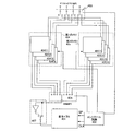
図1に本発明の実施形態を示す。図1は本実施の形態に係る表示装置のブロック図を示す。表示装置100は、コントローラ101、メモリ102、光センサ103、アンプ104、電源105、表示パネル106を含んでいる。
(Embodiment 1)
FIG. 1 shows an embodiment of the present invention. FIG. 1 is a block diagram of a display device according to this embodiment. The
コントローラ101は外部から入力される制御信号及び映像信号と、アンプ104から供給される光センサ信号に基づき、表示パネル106の駆動に必要な信号を生成する。そして、それらの信号を表示パネル106に供給する。メモリ102は主として映像信号を一時的に記憶するために用いられる。また、メモリ102は、映像信号以外の情報を記憶するためにも用いられる。光センサ103は外光(表示装置100が受ける外部の光)を検出する。その出力は、アンプ104に供給される。アンプ104は光センサ103が出力する電気信号を増幅し、増幅した電気信号をコントローラ101に供給する。なお、光センサ103が出力する電気信号が十分大きければ、アンプ104は省略することもできる。電源105は、表示パネル106に必要な電圧又は電流を供給する。なお、表示パネル106はエレクトロルミネセンス(EL)素子を用いたものである。その他にFED(フィールドエミッションディスプレイ)にも適用することができる。
The controller 101 generates a signal necessary for driving the display panel 106 based on a control signal and a video signal input from the outside and an optical sensor signal supplied from the
表示装置100は光センサ103の出力に基づき、表示パネル106の表示画面に表示する画像の総階調数を変える。光センサ103としては、フォトダイオード、フォトトランジスタを適用することができる。具体的には、表示装置100が強い外光を受けて、光センサ103の出力がある一定の値以上になると、表示パネル106の表示画面に表示する画像の総階調数を低くする。表示装置100が強い外光を受けると、ある階調目とある階調目との区別がはっきりせず、表示パネル106の表示画面に表示する画像がぼやけてしまう。しかしながら、上記のように、表示装置100が受ける外光に応じて、総階調数を低くすることにより、ある階調目とある階調目との区別を明確にして、表示パネル106の表示画面の視認性を向上させることができる。
The
また、光センサ103の出力により、表示パネル106の表示画面に表示する画像の総階調を2階調とする場合、通常では、白地の背景画像に黒地の表示画像を表示すが、それを反転させて黒地の背景画像に白地の表示画像を表示しても良い。そうすると、表示画面の視認性をさらに向上させることができる。また、白地の表示画像の輝度を高くすることにより、表示画面の視認性をさらに向上させることができる。この背景画像と表示画像の組み合わせは黒地に白表示に限定されず、コントラストのとりやすい(明暗比がはっきりする)組み合わせであれば任意の色の組み合わせをすることができる。
Further, when the total gradation of the image displayed on the display screen of the display panel 106 is set to two gradations by the output of the
光センサ103の出力は、アンプ104を介して、コントローラ101に送られる。コントローラ101は、光センサ103の出力がある一定の値以上であるかどうかを階調出力選択部108で検出する。光センサ103の出力がある一定の値以上ではない場合、表示パネル106に出力する映像信号の総階調数は変えない。一方、光センサ103の出力がある一定の値以上の場合、表示パネル106に出力する映像信号の総階調数を低くなるように補正する。映像信号の階調は階調変換部107で階調数を変化させる。そして、これらの映像信号をメモリ102に記憶させておく。そして、光センサ103の出力に基づき、外光に適した総階調数の映像信号を階調出力選択部108で選択して表示パネル106に供給する。
The output of the
表1に示すように、室内及び屋外の明るさは、照明の具合や天候などの気象条件、時刻などによりさまざまに変化する。例えば、照明のある室内における照度は800ルクスから1,000ルクス前後であり、昼間の曇天下における照度は32,000ルクス程度であり、昼間の晴天下の照度は100,000ルクスに達する。

このようなさまざまな明るさの状況下において、エレクトロルミネセンスを利用した表示パネル(ELパネル)、透過型液晶パネル(透過型LCDパネル)、半透過型液晶パネル(半透過型LCDパネル)、反射型液晶パネル(反射型LCD)の視認性を比較した結果を表2に示す。
結果として、1,500ルクス程度までの明るさ(主に室内、照明付きホールなど)の環境下では、ELパネル、反射型液晶パネルを除く各種液晶パネルで表示パターン(自然画、テキスト(文字、記号)など)によらず良好な視認性が得られた。これに対して、10,000ルクス下(昼間の曇天時)においては、ELパネル、透過型液晶パネルでは、自然画を表示した場合、中間調部分などの、コントラストが低い部分の視認度が大きく低下する傾向が見られた。しかしながら、この場合においても、ELパネルの方が透過型液晶パネルよりも視認性は良好であった。また、ELパネルにおいて、階調数を低下させた場合(2階調から8階調)視認性は回復し、特にテキスト表示においては実用上支障のない視認性が得られている。一方、半透過型液晶パネルでは、室内から屋外の環境下において、全体的にコントラストがやや低いものの、10,000ルクスの環境下で良好な視認性が得られた。消費電力に関しては、反射型液晶パネルが優れているが、室内などの比較的照度が低い環境下において視認性が低下する傾向が現れている。透過型液晶パネルでは、バックライトが電力を消費するので、反射型液晶パネルよりも消費電力が高くなっている。これに対し、ELパネルにおいては、階調数を低くした表示モードでは低消費電力化が図られている。 As a result, in environments with brightness up to about 1,500 lux (mainly indoors, illuminated halls, etc.), display patterns (natural images, text (characters, Good visibility was obtained regardless of the symbol). On the other hand, under 10,000 lux (during cloudy daytime), the EL panel and transmissive liquid crystal panel display a large amount of visibility in low contrast areas such as halftone areas when displaying natural images. There was a tendency to decrease. However, even in this case, the visibility of the EL panel was better than that of the transmissive liquid crystal panel. Further, in the EL panel, the visibility is restored when the number of gradations is reduced (from 2 to 8 gradations), and visibility that is practically satisfactory for text display is obtained. On the other hand, in the transflective liquid crystal panel, good visibility was obtained under an environment of 10,000 lux although the contrast was slightly low overall in an indoor to outdoor environment. In terms of power consumption, reflective liquid crystal panels are excellent, but there is a tendency for visibility to deteriorate in environments with relatively low illuminance such as indoors. In the transmissive liquid crystal panel, since the backlight consumes power, the power consumption is higher than that of the reflective liquid crystal panel. On the other hand, in the EL panel, low power consumption is achieved in the display mode in which the number of gradations is reduced.
表2から明らかなように、ELパネルを用い、外光強度に応じて階調数を調節した表示モードとすることにより、室内から屋外までの環境下において視認性を確保しつつ、低消費電力化を図った表示装置を提供することができる。 As can be seen from Table 2, the EL panel is used and the display mode is adjusted in the number of gradations according to the external light intensity, thereby ensuring visibility in an environment from indoors to outdoors while reducing power consumption. It is possible to provide a display device that achieves the above.
例えば、図1に示す表示装置100において、光センサ103の出力により、表示装置100が10ルクスから100ルクスの外光を受けていることが検出された場合、総階調数は64階調から1024階調として変化させない。また、光センサ103の出力により、表示装置100が100ルクスから1,000ルクスの外光を受けていることが検出された場合、総階調数を16階調から64階調に補正する。また、光センサ103の出力により、表示装置100が1,000ルクスから10,000ルクスの外光を受けていることが検出された場合、総階調数を4階調から16階調に補正する。また、光センサ103の出力により、表示装置100が10,000ルクスから100,000ルクスの外光を受けていることが検出された場合、総階調数を2階調から4階調に補正する。
外光の明るさに対する階調数の補正は、上記の例に限定されない。一般に、外光の強度がxルクスのとき階調数がi、外光の強度がyルクスのとき階調数がj、かつ外光の強度がzルクスのとき階調数がkである場合、自然数i、j、kが、式i>j>kをみたし、正の実数x、y、zが、式x<y<zを満たせばよい。
For example, in the
The correction of the number of gradations with respect to the brightness of outside light is not limited to the above example. Generally, the number of gradations is i when the intensity of external light is x lux, the number of gradations is j when the intensity of external light is y lux, and the number of gradations is k when the intensity of external light is z lux. The natural numbers i, j, and k satisfy the equation i>j> k, and the positive real numbers x, y, and z satisfy the equation x <y <z.
なお、コントローラ101には、外部からアナログの映像信号が供給される。表示パネル106の表示画面がアナログの階調表示を行う場合であって、標準の映像信号の総階調数が64階調である場合、予め総階調数が32階調、16階調、8階調、4階調の各々の映像信号を階調変換部107で生成しておき、これらの映像信号をメモリ102に記憶させておく。そして、光センサ103の出力に基づき、外光に適した総階調数の映像信号を階調出力選択部108で選択して表示パネル106に供給する。
The controller 101 is supplied with an analog video signal from the outside. In the case where the display screen of the display panel 106 performs analog gradation display, and the total number of gradations of the standard video signal is 64 gradations, the total number of gradations is 32 gradations, 16 gradations, Each of the video signals of 8 gradations and 4 gradations is generated by the gradation conversion unit 107, and these video signals are stored in the
また、表示パネル106の表示画面がデジタルの階調表示を行う場合、コントローラ101は、アナログの映像信号をデジタルの映像信号に変換する。そして、標準の映像信号の総階調数が6ビット(64階調)の場合、予め、5ビット(32階調)、4ビット(16階調)、3ビット(8階調)、2ビット(4階調)の映像信号を階調変換部107で生成しておく。そして、これらの映像信号をメモリ102に記憶させておく。そして、光センサ103の出力に基づき、外光に適した総階調数の映像信号を階調出力選択部108で選択してパネル306に供給する。
When the display screen of the display panel 106 performs digital gradation display, the controller 101 converts an analog video signal into a digital video signal. When the total number of gradations of the standard video signal is 6 bits (64 gradations), 5 bits (32 gradations), 4 bits (16 gradations), 3 bits (8 gradations), 2 bits in advance A video signal of (4 gradations) is generated by the gradation conversion unit 107 in advance. These video signals are stored in the
また、表示パネル106の表示画面が表示する画像によっても、階調数を変えると良い。例えば、静止画を表示する場合であって、文字やアイコンなどのテキストを表示するモードがある。この場合は、総階調数を2階調から8階調にする。また、静止画を表示する場合であって、画像を表示するモードがある。この場合は、総階調数を4階調から16階調にする。さらに、動画を表示するモードがある。この場合は、総階調数を16階調から64階調、若しくは16階調から1024階調にする。このように、各モードに従って、階調数を変えることで、消費電力を削減することができる。なお、上記のモードは、コントローラ101に供給される映像信号に基づき、コントローラ101が判別するようにしても良い。 The number of gradations may be changed depending on the image displayed on the display screen of the display panel 106. For example, there is a mode for displaying a still image and displaying text such as characters and icons. In this case, the total number of gradations is changed from 2 gradations to 8 gradations. Further, there is a mode for displaying still images and displaying images. In this case, the total number of gradations is changed from 4 gradations to 16 gradations. There is also a mode for displaying moving images. In this case, the total number of gradations is changed from 16 gradations to 64 gradations, or from 16 gradations to 1024 gradations. In this manner, power consumption can be reduced by changing the number of gradations according to each mode. The mode may be determined by the controller 101 based on the video signal supplied to the controller 101.
また、表示装置100に利用者が表示モードを選択する選択スイッチを設けても良い。そして、利用者が選択スイッチを操作することにより、上記のモードを選択しても良い。また、選択スイッチにより表示モードを選択した場合であっても、光センサ103の信号によって(外光強度)に応じて、選択されている表示モードの階調を自動的に増減しても良い。
The
図2に外光強度に応じて表示モードを切替可能な携帯電話の態様を示す。図2(A)に示す携帯電話は第1の筐体201、第2の筐体202、表示画面203、スピーカー204、アンテナ205、ヒンジ206、キーボード207、マイクロフォン208、光センサ209より構成されている。本発明の表示装置は第1の筐体201の中に装着されている。
FIG. 2 shows a mode of a mobile phone capable of switching the display mode in accordance with the external light intensity. A cellular phone illustrated in FIG. 2A includes a
図2(A)は外光が弱い場合の表示を示している。表示画面203においては白地の背景画像に黒文字が表示されている。外光が弱い場合、目の感度は表示画面の発光輝度に合わされる。
FIG. 2A shows a display when the outside light is weak. On the
図2(B)は外光が強い場合の表示を示している。外光が強い場合は白地の背景画像が外光に負けてしまうので、光センサ209において、外光の強度を検出し、背景画像を図2(B)に示すように黒地に変更する。このように背景画像を黒にすることにより、発光部分の面積を削減できる。そして少ない白の表示部分に、電力を集中することによって、白の部分をよりはっきりと表示することができる。
FIG. 2B shows a display when the outside light is strong. When the external light is strong, the white background image is lost to the external light. Therefore, the
本実施の形態においては携帯電話について示したが、それらに限定されず、PDA、ビデオカメラ、デジタルカメラ、携帯型DVD、携帯型テレビジョン、ゲーム機器、コンピュータなどさまざまな表示装置を用いる電子機器に使用が可能である。 Although mobile phones have been described in this embodiment mode, the present invention is not limited thereto, and the present invention is applied to electronic devices using various display devices such as PDAs, video cameras, digital cameras, portable DVDs, portable televisions, game machines, and computers. Can be used.
(実施の形態2)
実施の形態1で示す表示装置における画素の一構成例を示す。図3は時間階調方式で動作可能な表示装置の画素例を示している。図3で示す画素は薄膜トランジスタ(以下、「TFT」ともいう。)で構成されている。図3は発光素子303を時間階調で駆動する画素を示している。この画素は発光素子303、駆動TFT302、保持容量304、スイッチングTFT301によって構成されている。スイッチングTFT301のゲートはゲート信号線G1に接続され、ゲート信号線G1がハイになるとオンして、ソース信号線S1のデータを保持容量304と駆動TFT302のゲートに書き込む。駆動TFT302がオンすると電源供給線V1より電流が駆動TFT302を介して発光素子303に流れる。この状態は次の書き込みが行われるまで保持される。
(Embodiment 2)
One example of a pixel in the display device described in
図3(B)は時間階調のタイミングチャートを示したものである。この例では4ビットを例にとり説明を行うが、4ビットに限定されるものではない。1フレームは4つのサブフレームSF1からSF4によって構成されている。それぞれのサブフレームはアドレス期間Ta1からTa4(書き込み期間)とサスティン期間Ts1からTs4(点灯期間)によって構成される。サスティン期間Ts1:Ts2:Ts3:Ts4=8:4:2:1にすることによって、サスティン期間に各ビットが対応し、時間階調が可能になる。このとき、アドレス期間は点灯を行わず、アドレッシングのみを行っている。 FIG. 3B shows a timing chart of time gradation. In this example, description will be made by taking 4 bits as an example, but it is not limited to 4 bits. One frame is composed of four subframes SF1 to SF4. Each subframe is composed of an address period Ta1 to Ta4 (writing period) and a sustain period Ts1 to Ts4 (lighting period). By setting the sustain period Ts1: Ts2: Ts3: Ts4 = 8: 4: 2: 1, each bit corresponds to the sustain period, and time gradation is possible. At this time, lighting is not performed during the address period, and only addressing is performed.
(実施の形態3)
実施の形態2で示す表示装置において、実施の形態1で示すように、信号の明暗を反転した画像を作り出すシステムの一例を図4に示す。この例では4ビットのデジタル映像信号をサブフレーム変換しているが、特に4ビットには限定されない。以下に動作を説明する。まずコントロール回路402はデジタル映像信号をスイッチ403を介して、第1のメモリ404に入力する。第1フレームのデータが全て第1のメモリ404に入力されると、スイッチ403を第2のメモリ405に切り替え、第2フレームのデジタル映像信号を書き込んでいく。この手段によって、白地の背景画像に黒地の表示画像の組み合わせ、又は黒地の背景画像に白地の表示画像の組み合わせを表示することが可能である。映像信号選択スイッチ406の出力はスイッチ407に入力され、映像信号選択スイッチ406の信号がそのまま表示パネル401に入力されるか、反転して入力されるかを選択できる。明暗反転が必要な場合には反転して入力を行えば良い。この選択はディスプレイコントローラによって行われる。
(Embodiment 3)
In the display device shown in
(実施の形態4)
図5に両面発光表示パネルを用いた携帯電話機の一態様を示す。図5に示す携帯電話は第1の筐体501、第2の筐体502、第1の表示画面503、第2の表示画面504、第3の表示画面505、スピーカー506、アンテナ507、ヒンジ508、キーボード509、マイクロフォン510、バッテリー511、光センサより構成されている。図5は外光が強く背景画像が黒地になった状態を示している。図5(A)は内側を開いた図を示しており、図5(B)は外側を示しており、図5(C)は側面を示している。本発明の表示装置は第1の筐体501の中に装着されている。
(Embodiment 4)
FIG. 5 illustrates one mode of a mobile phone using a double-sided light emitting display panel. A cellular phone illustrated in FIG. 5 includes a
また、図5において、第1の表示画面503はメインディスプレイであり、第2の表示画面504はサブディスプレイであり2画面配置されている場合を例示しているが、その数に限定はない。サブディスプレイの表示面積は、主ディスプレイの表示面積よりも小さい構成となっている。
In FIG. 5, the
このような携帯電話機において、図4に示すシステムは、コントロール回路、メモリ回路を用いても映像を左右反転することを可能としている。図4において、まずコントロール回路402はデジタル映像信号をスイッチ403を介して、第1のメモリ404に入力する。第1フレームのデータが全て第1のメモリ404に入力されると、スイッチ403を第2のメモリ405に切り替え、第2フレームのデジタル映像信号を書き込んでいく。
In such a cellular phone, the system shown in FIG. 4 is capable of reversing the image horizontally using a control circuit and a memory circuit. In FIG. 4, first, the
一方、映像信号選択スイッチ406はその間に第1のメモリ404(1)から第1のメモリ404(4)に順次接続され、第1のメモリ404に蓄えられた信号を表示パネル401に入力する。そして、第2フレームのデータが全て第2のメモリ405に入力されると、スイッチ403を第1のメモリ404に切り替え、第3フレームのデジタル映像信号を書き込んでいく。また、映像信号選択スイッチ406はその間に第2のメモリ405(1)から第2のメモリ405(4)に順次接続され、第2のメモリ405に蓄えられた信号を表示パネル401に入力する。以上を繰り返すことによりサブフレームを形成できる。
On the other hand, the video
映像を左右反転する場合には第1のメモリ404又は第2のメモリ405を呼び出すときに、ディスプレイの1列毎の信号を逆に呼び出すことによって可能となる。このようにサブフレーム変換を行う表示装置では、メモリの呼び出し順序を変えることにより両面発光の対応が可能となる。
When the video is reversed left and right, when the
(実施の形態5)
図6は実施の形態4の携帯電話機に用いる両面発光表示パネル概念を示す。図6では2つの透明基板601、602の間に透明電極又はそれに準ずる電極603、電極604、電極605及び電極609が存在し、それらの電極間にエレクトロルミネセンスを発現するEL層606、EL層607、EL層608を挟んでいる。透明基板601にはカラーフィルタ610、カラーフィルタ611、カラーフィルタ612が配置され、EL層606、EL層607、EL層608が白発光の場合には第1の発光面にはフルカラー表示が、第2の発光面には白表示が可能となる。カラーフィルタを用いずに発光体を色塗り分けしても良い、その場合第1の発光面と第2の発光面に表示できる色は同じとなる。
(Embodiment 5)
FIG. 6 shows a concept of a double-sided light emitting display panel used in the mobile phone of the fourth embodiment. In FIG. 6, a transparent electrode or an
(実施の形態6)
実施の形態1乃至5に示す表示装置の画素の構成の一態様について、図7を参照して説明する。図7は、薄膜トランジスタ(TFT)とそれに接続する発光素子で構成される画素の断面図である。
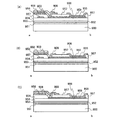
(Embodiment 6)
One mode of a pixel structure of the display device described in any of
図7において、基板700上に、ブロッキング層701、TFT750を構成する半導体層702、容量部751の一方の電極を構成する半導体層712が形成されている。その上層には第1絶縁層703が形成され、TFT750にあってはゲート絶縁層として、容量部751にあっては容量を形成するための誘電体層として機能する。
In FIG. 7, a
第1絶縁層703上にはゲート電極704と容量部751の他方の電極を形成する導電層754が形成されている。TFT750に接続する配線707は、発光素子752の第1電極708と接続している。この第1電極708は、第3絶縁層706上に形成されている。第1絶縁層703と第3絶縁層706との間には、第2絶縁層705が形成されていても良い。発光素子752は、第1電極708、EL層709、第2電極710で構成されている。また、第1電極708の周辺端部及び、第1電極708と配線707との接続部を覆うように第4絶縁層711が形成されている。
A conductive layer 754 that forms the
次に、上記に示す構成の詳細を説明する。基板700としては、例えばバリウムホウケイ酸ガラスや、アルミノホウケイ酸ガラスなどのガラス基板、石英基板、セラミック基板等を用いることができる。また、ステンレスを含む金属基板又は半導体基板の表面に絶縁膜を形成したものを用いても良い。プラスチック等の可撓性を有する合成樹脂からなる基板を用いても良い。基板700の表面を、科学的機械研磨(CMP)法などの研磨により平坦化しておいても良い。
Next, the detail of the structure shown above is demonstrated. As the
ブロッキング層701としては、酸化珪素や、窒化珪素又は窒化酸化珪素などの絶縁膜を用いることができる。ブロッキング層701によって、基板700に含まれるNaなどのアルカリ金属やアルカリ土類金属が半導体層702に拡散しTFT750の特性に悪影響をおよぼすのを防ぐことができる。図7では、ブロッキング層701を単層の構造としているが、2層あるいはそれ以上の複数層で形成しても良い。なお、石英基板など不純物の拡散がさして問題とならない場合は、ブロッキング層701を必ずしも設ける必要はない。
As the
また、マイクロ波で励起され、電子温度が2eV以下、イオンエネルギーが5eV以下、電子密度が1×10¹¹から5×10¹³/cm3程度までである高密度プラズマで、ガラス基板の表面を直接処理しても良い。プラズマの生成はラジアルスロットアンテナを用いたマイクロ波励起のプラズマ処理装置を用いることができる。このとき、窒素(N2)、又はアンモニア(NH3)、亜酸化窒素(N2O)などの窒化物気体を導入すると、ガラス基板の表面を窒化することができる。このガラス基板の表面に形成された窒化物層は、窒化珪素を主成分とするので、ガラス基板側から拡散してくる不純物のブロッキング層として利用することができる。この窒化物層の上に酸化珪素膜又は酸窒化珪素膜をプラズマCVD法で形成してブロッキング層701としても良い。
In addition, the surface of the glass substrate is directly irradiated with high-density plasma excited by microwaves, having an electron temperature of 2 eV or less, an ion energy of 5 eV or less, and an electron density of about 1 × 10 11 to 5 × 10 13 / cm 3. It may be processed. Plasma generation can be performed using a microwave-excited plasma processing apparatus using a radial slot antenna. At this time, when a nitride gas such as nitrogen (N 2 ), ammonia (NH 3 ), or nitrous oxide (N 2 O) is introduced, the surface of the glass substrate can be nitrided. Since the nitride layer formed on the surface of the glass substrate contains silicon nitride as a main component, it can be used as a blocking layer for impurities diffused from the glass substrate side. A
他にも、酸化珪素や、酸窒化珪素などによるブロッキング層701の表面に対し同様なプラズマ処理を行うことにより、その表面及び表面から1nmから10nmの深さで窒化処理をすることができる。このきわめて薄い窒化珪素の層により、その上に形成する半導体層へ応力の影響を与えることなくブロッキング層とすることができる。
In addition, by performing similar plasma treatment on the surface of the
半導体層702及び半導体層712としては、島状に分割された結晶性半導体膜を用いることが好ましい。結晶性半導体膜は非晶質半導体膜を結晶化して得ることができる。結晶化方法としては、レーザ結晶化法、RTA又はファーネスアニール炉を用いる熱結晶化法、結晶化を助長する金属元素を用いる熱結晶化法等を用いることができる。半導体層702は、チャネル形成領域と、一導電型を付与する不純物元素が添加された一対の不純物領域とを有する。なお、チャネル形成領域と一対の不純物領域との間に、前記不純物元素が低濃度で添加された不純物領域を有していても良い。半導体層712には、全体に一導電型若しくはそれと逆の導電型を付与する不純物元素が添加された構成とすることができる。
As the
第1絶縁層703としては、酸化珪素、窒化珪素又は窒化酸化珪素等を用い、単層又は複数の膜を積層させて形成することができる。この場合において、当該絶縁膜の表面を、前述と同様に、マイクロ波で励起され、電子温度が2eV以下、イオンエネルギーが5eV以下、電子密度が1×10¹¹から5×10¹³/cm3程度までである高密度プラズマ処理によって酸化又は窒化処理して緻密化しても良い。この処理は第1絶縁層703の成膜に先立って行っても良い。すなわち、半導体層702の表面に対してプラズマ処理を行う。このとき、基板温度を300℃から450℃とし、酸化雰囲気(O2、N2Oなど)又は窒化雰囲気(N2、NH3など)で処理することにより、その上に堆積するゲート絶縁層と良好な界面を形成することができる。
The first insulating
ゲート電極704及び導電層754としては、Ta、W、Ti、Mo、Al、Cu、Cr、Ndから選ばれた一種の元素又は該元素を複数含む合金若しくは化合物からなる単層又は積層構造を用いることができる。
As the
TFT750は、半導体層702と、ゲート電極704と、半導体層702とゲート電極704との間の第1絶縁層703とによって構成される。図7では、画素を構成するTFT750として、発光素子752の第1電極708に接続されるものを示している。このTFT750は、ゲート電極704を半導体層702上に複数配置したマルチゲート型の構成を示している。すなわち、複数のTFTが直列に接続された構成を有している。このような構成により、不用意なオフ電流の増加を抑制することができる。なお、また、図7では、TFT750をトップゲート型のTFTとして示したが、半導体層の下方にゲート電極を有するボトムゲート型のTFTであっても良いし、半導体層の上下にゲート電極を有するデュアルゲート型のTFTであっても良い。
The
容量部751は、第1絶縁層703を誘電体とし、第1絶縁層703を挟んで対向する半導体層712と導電層754とを一対の電極として構成される。なお、図7では、画素に設ける容量素子として、一対の電極の一方をTFT750の半導体層702と同時に形成される半導体層712とし、他方の導電層754をゲート電極704と同時に形成される層とする例を示したが、この構成に限定されない。
The
第2絶縁層705は窒化珪素膜などイオン性不純物をブロッキングするバリア性の絶縁膜であることが望ましい。この第2絶縁層705は窒化シリコン又は酸窒化シリコンで形成する。この第2絶縁層705は、半導体層702の汚染を防ぐ保護膜としての機能を含んでいる。この第2絶縁層705を堆積した後に、水素ガスを導入して前述のようにマイクロ波で励起された高密プラズマ処理をすることで、第2絶縁層705の水素化を行っても良い。又は、アンモニアガスを導入して、第2絶縁層705の窒化と水素化を行っても良い。又は、酸素、N2Oガスなどと水素ガスを導入して、酸化窒化処理と水素化処理を行っても良い。この方法により、窒化処理、酸化処置若しくは酸化窒化処理を行うことにより第2絶縁層705の表面を緻密化することができる。それにより保護膜としての機能を強化することができる。この第2絶縁層705に導入された水素は、その後400℃から450℃の熱処理をすることにより、第2絶縁層705を形成する窒化シリコンから水素を放出させて、半導体層702の水素化をすることができる。
The second
第3絶縁層706としては、無機絶縁膜や有機絶縁膜を用いることができる。無機絶縁膜としては、CVD法により形成された酸化シリコン膜や、SOG(Spin On Glass)膜(塗布酸化珪素膜)などを用いることができる。有機絶縁膜としてはポリイミド、ポリアミド、BCB(ベンゾシクロブテン)、アクリル又はポジ型感光性有機樹脂、ネガ型感光性有機樹脂等の膜を用いることができる。また、第3絶縁層706として、シリコン(Si)と酸素(O)との結合で骨格構造が構成される材料を用いることができる。この材料の置換基として、少なくとも水素を含む有機基(例えばアルキル基、芳香族炭化水素)が用いられる。置換基として、フルオロ基を用いても良い。又は置換基として、少なくとも水素を含む有機基と、フルオロ基とを用いても良い。
As the third insulating
配線707としては、Al、Ni、C、W、Mo、Ti、Pt、Cu、Ta、Au、Mnから選ばれた一種の元素又は該元素を複数含む合金からなる単層又は積層構造を用いることができる。
As the
第1電極708及び第2電極710の一方若しくは両方を透明電極とすることができる。透明電極としては、酸化タングステンを含む酸化インジウム、酸化タングステンを含む酸化インジウム酸化亜鉛、酸化チタンを含む酸化インジウム酸化スズ、酸化チタンを含む酸化インジウム酸化スズ、モリブデン含む酸化インジウム酸化スズなどを用いることができる。勿論、酸化インジウム酸化スズ、酸化インジウム酸化亜鉛、酸化珪素を添加した酸化インジウム酸化スズなども用いることができる。
One or both of the
第1電極708及び第2電極710の少なくとも一方は、透光性を有さない材料で形成されていても良い。例えば、LiやCs等のアルカリ金属、及びMg、Ca、Sr等のアルカリ土類金属、これらを含む合金(Mg:Ag、Al:Li、Mg:Inなど)、及びこれらの化合物(CaF2)の他、YbやEr等の希土類金属を用いることができる。
At least one of the
第4絶縁層711としては、第3絶縁層706と同様の材料を用いて形成することができる。
The fourth insulating
発光素子752は、EL層709と、それを挟む第1電極708及び第2電極710とによって構成される。第1電極708及び第2電極710の一方が陽極に相当し、他方が陰極に相当する。発光素子752は、陽極と陰極の間にしきい値電圧より大きい電圧が順バイアスで印加されると、陽極から陰極に電流が流れて発光する。
The
EL層709は、単数又は複数の層で構成されている。複数の層で構成されている場合、これらの層は、キャリア輸送特性の観点から正孔注入層、正孔輸送層、発光層、電子輸送層、電子注入層などに分類することができる。なお各層の境目は必ずしも明確である必要はなく、互いの層を構成している材料が一部混合し、界面が不明瞭になっている場合もある。各層には、有機系の材料、無機系の材料を用いることが可能である。有機系の材料として、高分子系、中分子系、低分子系のいずれの材料も用いることが可能である。
The
EL層709は、正孔注入輸送層、発光層、電子注入輸送層など、機能の異なる複数の層を用いて構成することが好ましい。正孔注入輸送層は、ホール輸送性の有機化合物材料と、その有機化合物材料に対して電子受容性を示す無機化合物材料とを含む複合材料で形成することが好ましい。このような構成とすることで、本来内在的なキャリアをほとんど有さない有機化合物に多くのホールキャリアが発生し、極めて優れたホール注入性・輸送性が得られる。この効果により、従来よりも駆動電圧を低くすることができる。また、駆動電圧の上昇を招くことなく正孔注入輸送層を厚くすることができるため、ゴミ等に起因する発光素子の短絡も抑制することができる。
The
ホール輸送性の有機化合物材料としては、例えば、銅フタロシアニン(略称:CuPc)、4,4’,4’’−トリス[N−(3−メチルフェニル)−N−フェニルアミノ]トリフェニルアミン(略称:MTDATA)、1,3,5−トリス[N,N−ジ(m−トリル)アミノ]ベンゼン(略称:m−MTDAB)、N,N’−ジフェニル−N,N’−ビス(3−メチルフェニル)−1,1’−ビフェニル−4,4’−ジアミン(略称:TPD)、4,4’−ビス[N−(1−ナフチル)−N−フェニルアミノ]ビフェニル(略称:NPB)、4,4’−ビス{N−[4−ジ(m−トリル)アミノ]フェニル−N−フェニルアミノ}ビフェニル(略称:DNTPD)、などが挙げられるが、これらに限定されることはない。 Examples of the hole transporting organic compound material include copper phthalocyanine (abbreviation: CuPc), 4,4 ′, 4 ″ -tris [N- (3-methylphenyl) -N-phenylamino] triphenylamine (abbreviation). : MTDATA), 1,3,5-tris [N, N-di (m-tolyl) amino] benzene (abbreviation: m-MTDAB), N, N′-diphenyl-N, N′-bis (3-methyl) Phenyl) -1,1′-biphenyl-4,4′-diamine (abbreviation: TPD), 4,4′-bis [N- (1-naphthyl) -N-phenylamino] biphenyl (abbreviation: NPB), 4 , 4′-bis {N- [4-di (m-tolyl) amino] phenyl-N-phenylamino} biphenyl (abbreviation: DNTPD), and the like, but is not limited thereto.
電子受容性を示す無機化合物材料としては、酸化チタン、酸化ジルコニウム、酸化バナジウム、酸化モリブデン、酸化タングステン、酸化レニウム、酸化ルテニウム、酸化亜鉛などが挙げられる。特に酸化バナジウム、酸化モリブデン、酸化タングステン、酸化レニウムは真空蒸着が可能で扱いやすいため、好適である。 Examples of the inorganic compound material that exhibits electron acceptability include titanium oxide, zirconium oxide, vanadium oxide, molybdenum oxide, tungsten oxide, rhenium oxide, ruthenium oxide, and zinc oxide. Vanadium oxide, molybdenum oxide, tungsten oxide, and rhenium oxide are particularly preferable because they can be vacuum-deposited and are easy to handle.
電子注入輸送層は、電子輸送性の有機化合物材料を用いて形成する。具体的には、トリス(8−キノリノラト)アルミニウム(略称:Alq3)、トリス(4−メチル−8−キノリノラト)アルミニウム(略称:Almq3)、ビス(2−メチル−8−キノリノラト)(4−フェニルフェノラト)アルミニウム(略称:BAlq)、バソキュプロイン(略称:BCP)、2−(4−ビフェニリル)−5−(4−tert−ブチルフェニル)−1,3,4−オキサジアゾール(略称:PBD)、3−(4−ビフェニリル)−4−フェニル−5−(4−tert−ブチルフェニル)−1,2,4−トリアゾール(略称:TAZ)、などが挙げられるが、これらに限定されることはない。 The electron injecting and transporting layer is formed using an organic compound material having an electron transporting property. Specifically, tris (8-quinolinolato) aluminum (abbreviation: Alq 3 ), tris (4-methyl-8-quinolinolato) aluminum (abbreviation: Almq 3 ), bis (2-methyl-8-quinolinolato) (4- Phenylphenolato) aluminum (abbreviation: BAlq), bathocuproin (abbreviation: BCP), 2- (4-biphenylyl) -5- (4-tert-butylphenyl) -1,3,4-oxadiazole (abbreviation: PBD) ), 3- (4-biphenylyl) -4-phenyl-5- (4-tert-butylphenyl) -1,2,4-triazole (abbreviation: TAZ), and the like. There is no.
EL層は、9,10−ジ(2−ナフチル)アントラセン(略称:DNA)、9,10−ジ(2−ナフチル)−2−tert−ブチルアントラセン(略称:t−BuDNA)、4,4’−ビス(2,2−ジフェニルビニル)ビフェニル(略称:DPVBi)、クマリン30、クマリン6、クマリン545、クマリン545T、ルブレン、2,5,8,11−テトラ(tert−ブチル)ペリレン(略称:TBP)、9,10−ジフェニルアントラセン(略称:DPA)、5,12−ジフェニルテトラセン、4−(ジシアノメチレン)−2−メチル−[p−(ジメチルアミノ)スチリル]−4H−ピラン(略称:DCM1)、4−(ジシアノメチレン)−2−メチル−6−[2−(ジュロリジン−9−イル)エテニル]−4H−ピラン(略称:DCM2)などが挙げられる。また、ビス{2−[3’,5’−ビス(トリフルオロメチル)フェニル]ピリジナト−N,C2’}イリジウム(ピコリナート)(略称:Ir(CF3ppy)2(pic))、トリス(2−フェニルピリジナト−N,C2’)イリジウム(略称:Ir(ppy)3)、ビス(2−フェニルピリジナト−N,C2’)イリジウム(アセチルアセトナート)(略称:Ir(ppy)2(acac))、ビス[2−(2’−チエニル)ピリジナト−N,C3’]イリジウム(アセチルアセトナート)(略称:Ir(thp)2(acac))、ビス(2−フェニルキノリナト−N,C2’)イリジウム(アセチルアセトナート)(略称:Ir(pq)2(acac))、などの燐光を放出できる化合物用いることもできる。
The EL layer is composed of 9,10-di (2-naphthyl) anthracene (abbreviation: DNA), 9,10-di (2-naphthyl) -2-tert-butylanthracene (abbreviation: t-BuDNA), 4,4 ′. -Bis (2,2-diphenylvinyl) biphenyl (abbreviation: DPVBi), coumarin 30,
また、EL層は一重項励起発光材料と金属錯体などを含む三重項励起材料を用いても良い。例えば、赤色の発光性の画素、緑色の発光性の画素及び青色の発光性の画素のうち、輝度半減時間が比較的短い赤色の発光性の画素を三重項励起発光材料で形成し、他を一重項励起発光材料で形成する。三重項励起発光材料は発光効率が良いので、同じ輝度を得るのに消費電力が少なくて済むという特徴がある。すなわち、赤色画素に適用した場合、発光素子に流す電流量が少なくて済むので、信頼性を向上させることができる。低消費電力化として、赤色の発光性の画素と緑色の発光性の画素とを三重項励起発光材料で形成し、青色の発光性の画素を一重項励起発光材料で形成しても良い。人間の視感度が高い緑色の発光素子も三重項励起発光材料で形成することで、より低消費電力化を図ることができる。 Further, a triplet excitation material including a singlet excitation light emitting material and a metal complex may be used for the EL layer. For example, among red light emitting pixels, green light emitting pixels, and blue light emitting pixels, a red light emitting pixel having a relatively short luminance half time is formed of a triplet excitation light emitting material, and the other A singlet excited light emitting material is used. The triplet excited luminescent material has a feature that the light emission efficiency is good, so that less power is required to obtain the same luminance. That is, when applied to a red pixel, the amount of current flowing through the light emitting element can be reduced, so that reliability can be improved. As a reduction in power consumption, a red light-emitting pixel and a green light-emitting pixel may be formed using a triplet excitation light-emitting material, and a blue light-emitting pixel may be formed using a singlet excitation light-emitting material. By forming a green light-emitting element having high human visibility with a triplet excited light-emitting material, power consumption can be further reduced.
EL層は、発光波長帯の異なる発光層を画素毎に形成して、カラー表示を行う構成としても良い。典型的には、R(赤)、G(緑)、B(青)の各色に対応した発光層を形成する。この場合にも、画素の光放射側にその発光波長帯の光を透過するフィルタを設けた構成とすることで、色純度の向上や、画素部の鏡面化(映り込み)の防止を図ることができる。フィルタを設けることで、従来必要であるとされていた円偏光板などを省略することが可能となり、発光層から放射される光の損失を無くすことができる。さらに、斜方から画素部(表示画面)を見た場合に起こる色調の変化を低減することができる。 The EL layer may be configured to perform color display by forming a light emitting layer having a different emission wavelength band for each pixel. Typically, a light emitting layer corresponding to each color of R (red), G (green), and B (blue) is formed. In this case as well, it is possible to improve the color purity and prevent mirror reflection (reflection) of the pixel portion by providing a filter that transmits light in the emission wavelength band on the light emission side of the pixel. Can do. By providing the filter, it is possible to omit a circularly polarizing plate that has been conventionally required, and the loss of light emitted from the light emitting layer can be eliminated. Furthermore, a change in color tone that occurs when the pixel portion (display screen) is viewed obliquely can be reduced.
図7で示す構成の画素と外光強度検出手段とを組み合わせることで、発光素子の発光時間を変化させ表示画面の輝度を制御することができる。また、外光強度検出手段により発光素子の発光を制御することにより、無用に点灯時間が増大しりことがないので、表示パネルの消費電力の低減と、寿命時間を延ばすことができる。 By combining the pixel having the configuration shown in FIG. 7 and the external light intensity detection means, the luminance of the display screen can be controlled by changing the light emission time of the light emitting element. Further, by controlling the light emission of the light emitting element by the external light intensity detecting means, the lighting time does not increase unnecessarily, so that the power consumption of the display panel can be reduced and the lifetime can be extended.
(実施の形態7)
外光の強度を検出する光センサは表示装置の一部に組み込まれていても良い。この光センサは部品として表示装置に実装されていても良いし、表示パネルに一体形成されていても良い。表示パネルに一体形成されている場合には、表示面を光センサの受光面として併用することができ、意匠上すぐれた効果を発揮する。すなわち表示装置に光センサが付属していることを意識させることなく、その外光強度に基づく階調制御を行うことができる。
(Embodiment 7)
An optical sensor that detects the intensity of external light may be incorporated in a part of the display device. This optical sensor may be mounted on the display device as a component, or may be integrally formed on the display panel. In the case of being integrally formed on the display panel, the display surface can be used together as the light receiving surface of the photosensor, and an excellent design effect is exhibited. In other words, gradation control based on the intensity of external light can be performed without making the display device conscious of the fact that an optical sensor is attached.
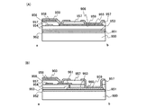
図8は表示パネル上に光センサを一体形成する一態様を示す図である。なお、図8では、エレクトロルミネセンスによる発光をする発光素子とその動作を制御するTFTで画素を構成する場合を示している。 FIG. 8 is a diagram showing an embodiment in which a photosensor is integrally formed on a display panel. Note that FIG. 8 shows a case where a pixel is formed by a light-emitting element that emits light by electroluminescence and a TFT that controls the operation thereof.
図8は、透光性を有する基板800上に形成された駆動用TFT801、透光性材料により形成された第1の電極802(画素電極)、EL層803及び透光性材料により形成された第2の電極804(対向電極)が設けられている。発光素子825は上方(矢印方向)に発光する。そして、第2の電極804上に形成された絶縁膜812上に、p型層831、実質的に真性なi型層832及びn型層833の積層体からなる光電変換素子838と、p型層831に接続されたp層側電極830、n型層833に接続されたn層側電極834が設けられる。
FIG. 8 illustrates a driving
本実施例では光センサ素子として光電変換素子838を用いる。発光素子825及び光電変換素子838は同一の基板800上に形成されており、発光素子825から発せられる光は、映像を構成し、ユーザーが視認する。一方、光電変換素子は外光を検出し、検出信号をコントローラに送る役割を持つ。このようにして、発光素子と光センサ(光電変換素子)を同一基板上に作製でき、セットの小型化に貢献できる。
In this embodiment, a
(実施の形態8)
実施の形態1乃至7のいずれか一若しくはその組み合わせの構成を備える表示パネルの構成を図9に示す。基板900上にゲート線駆動回路901、データ線駆動回路902、対向電極903、接続端子部905を有する。そしてシール領域904は、基板900と対向基板とを貼り合わせるための領域である。よって、基板900と対向基板がシール領域において張り合わされると、基板900と対向基板とシール材によって、ゲート線駆動回路901、データ線駆動回路902及び対向電極903は封入されることになる。
(Embodiment 8)
FIG. 9 illustrates a structure of a display panel including any one of
なお、対向電極903の下層には、データ線駆動回路902から列方向に延びた複数のソース線が行方向に並んで配列している。また、ゲート線駆動回路901から行方向に延びた複数のゲート線が列方向に並んで配列している。また、ソース線やゲート線に対応して、表示素子を含む複数の画素がマトリクスに配列している。
Note that a plurality of source lines extending in the column direction from the data
なお、表示素子は、EL素子(有機EL素子、無機EL素子又は有機物及び無機物を含むEL素子)、フィールドエミッションディスプレイ(FED)で用いる素子、FEDの一種であるSED(Surface−conduction Electron−emitter Display)、液晶ディスプレイ(LCD)、プラズマディスプレイ(PDP)、電子ペーパーディスプレイ、デジタルマイクロミラーデバイス(DMD)、圧電セラミックディスプレイなど、さまざまなものが含まれる。 Note that the display element is an EL element (an organic EL element, an inorganic EL element, or an EL element including an organic substance and an inorganic substance), an element used in a field emission display (FED), or a SED (Surface-Conduction Electron-Emitter Display) which is a kind of FED. ), Liquid crystal display (LCD), plasma display (PDP), electronic paper display, digital micromirror device (DMD), piezoelectric ceramic display, and the like.
また、基板上に形成された接続端子部905には複数の接続端子が配列されている。これらの接続端子は、基板900上に形成された回路に外部から入力される信号や電源を供給するために、外部の回路と接続するための端子である。基板900上に形成された回路とは、画素が有する薄膜トランジスタ(TFTともいう)の形成と同時に作り込まれた薄膜トランジスタなどから構成される回路はもちろんのこと、ICチップ上に形成した回路が基板900上にCOG(Chip On Glass:チップオングラス)などによって実装されているものも含まれる。なお、ICチップとは、基板上に形成された集積回路をチップ上に切り離したものをいう。特に、ICチップとしては、単結晶シリコンウエハを基板に用いて、素子分離などにより回路を形成し、単結晶シリコンウエハを任意の形状に切り離したものが適している。また、外部の回路と接続するための接続端子部905には、例えば、FPC(Flexible Print Circuit:フレキシブルプリントサーキット)などが電気的に接続される。
A plurality of connection terminals are arranged in the
よって、接続端子と接続された配線により、データ線駆動回路902やゲート線駆動回路901に信号や電源が供給され、画素電極や対向電極に電源が供給されている。
Therefore, signals and power are supplied to the data
ここで、本実施例の表示装置は、データ線駆動回路902が対向電極903を挟んで、接続端子部905とは反対側に形成されている。つまり、接続端子部905と対向電極903の間にはデータ線駆動回路902が配置されていない。よって、対向電極903に入力する電源電位が入力されている接続端子906と一続きの配線は、データ線駆動回路をまたぐことなく、コンタクトホール907を介して対向電極903と接続される。
Here, in the display device of this embodiment, the data
つまり、この構成によれば、対向電極903がデータ線駆動回路902上をまたぐことがないので、対向電極903がデータ線駆動回路902と重なることにより生じる寄生容量の発生を防止することができる。
In other words, according to this configuration, since the
また、多層配線構造により、データ線駆動回路902をくぐり抜けて接続端子906と対向電極903とを接続すると、配線同士の接触抵抗の増加を招いてしまう。しかし、本構成によれば、多層配線構造にせずに接続端子906と対向電極903とを接続することができるため低抵抗化を図ることができる。また、接続端子906と対向電極903との距離が短いため、配線抵抗も小さくすることができる。
Further, when the
次に、接続端子906と対向電極903との接続についてさらに詳しく説明するため、図9の線ab間の断面図を用いて説明する。図10(A)が、図9の線ab間の断面の一例を示す図である。
Next, the connection between the
基板900上に下地層951を有している。基板900としてはガラス基板、石英基板、プラスチック基板、セラミック基板等の絶縁性基板、金属基板、半導体基板等を用いることができる。
A
下地層951はCVD法やスパッタ法により形成することができる。例えばSiH4、N2O、NH3を原料に用いたCVD法により形成した酸化珪素膜、窒化珪素膜、酸化窒化珪素膜等を適用することができる。また、これらの積層を用いても良い。なお、下地層951は基板900から不純物が半導体層に拡散することを防ぐために設けるものであり、基板900にガラス基板や石英基板を用いている場合には下地層951は設けなくても良い。
The
下地層951上にゲート絶縁膜952を有している。ゲート絶縁膜952としてはCVD法やスパッタ法により形成される酸化珪素膜、窒化珪素膜、酸化窒化珪素膜等を用いることができる。
A
ゲート絶縁膜952上には層間絶縁膜を有している。層間絶縁膜は下層絶縁膜953と上層絶縁膜954を有している。下層絶縁膜953としては、例えば無機絶縁膜を適用することができる。無機絶縁膜としては、窒化珪素膜、酸化珪素膜、酸化窒化珪素膜又はこれらを積層した膜を用いることができる。また、上層絶縁膜としては、無機絶縁膜又は樹脂膜を適用することができる。無機絶縁膜としては、上述したものを用いることができ、樹脂膜としては、ポリイミド、ポリアミド、アクリル、ポリイミドアミド、エポキシなどを用いることができる。
An interlayer insulating film is provided over the
また、層間絶縁膜上には、配線955及び配線956を有している。なお、配線955及び配線956は同じ層に同じ材料の導電膜で形成され、これらの材料としては、チタン(Ti)膜やアルミニウム(Al)膜や銅(Cu)膜やTiを含むアルミニウム膜などを用いることができる。より好ましくは、配線955及び配線956は、三層構造とし、下層にチタン(Ti)膜、その上にアルミニウム(Al)膜、さらにその上にチタン(Ti)膜という構造を用いる。
In addition, a
なお、配線955は図9の接続端子906の配線に相当する。また、配線956はシール領域904内の配線に相当する。そして、この層の同じ材料によって形成されたシール領域904内の配線には、トランジスタの不純物領域と接する配線が含まれる。
Note that the
また、配線956や配線955上に絶縁層957が形成されている。例えば、絶縁層957としては、ポジ型の感光性アクリル樹脂膜を用いることができる。
An insulating
また、絶縁層957上にEL層958を有する。また、EL層958上に対向電極903及び接続電極959を有している。絶縁層957にはコンタクトホールが形成されており、コンタクトホールを介して、対向電極903は配線955と接続されている。また、接続電極959も配線955と接続されている。よって、接続端子906は、配線955の一部と接続電極959により構成され、接続電極959が接続端子906の接続パッドに相当する。
Further, an
図9に示す構成は、特に画面サイズが1インチから3インチ程度の表示パネルに適用すると好ましい。 The configuration shown in FIG. 9 is particularly preferably applied to a display panel having a screen size of about 1 to 3 inches.
なお、上述した断面図10(A)は一例であってこれに限定されない。他の構成を図10(B)に示す。なお、ここでは、図10(A)と共通するところは共通の符号を用いてその説明を省略する。 Note that the above-described cross-sectional view 10A is an example, and the present invention is not limited to this. Another structure is shown in FIG. Note that the same reference numerals are used for portions common to FIG. 10A, and description thereof is omitted.
図10(B)の構成は、ゲート絶縁膜952上に配線960を有する。なお、配線960は図9の接続端子906の一部と、接続端子906と一続きの配線に相当する。そして、この配線960と同じ層の同じ材料によって形成されたシール領域内の配線には、トランジスタのゲート電極を構成しているものが含まれる。
The structure in FIG. 10B includes a
そして、配線960上には層間絶縁膜(下層絶縁膜953及び上層絶縁膜954)を有している。そして、上層絶縁膜954上に配線956と配線961を有し、配線961はコンタクトホールを介して配線960と接続されている。また、配線956はシール領域904内の配線に相当する。そして、この層の同じ材料によって形成されたシール領域904内の配線には、トランジスタの不純物領域と接する配線が含まれる。
An interlayer insulating film (a lower insulating
さらに配線956、配線961及び上層絶縁膜954上には絶縁層957を有している。そして、絶縁層957上であってシール領域内にEL層958が形成されている。そして、シール領域内でのEL層958及び絶縁層957上には対向電極903が形成されている。また、接続端子部の絶縁層957上には、接続電極959が形成されている。そして、シール領域内の対向電極903はコンタクトホールを介して配線961と接続され、接続端子部の接続電極959はコンタクトホールを介して配線960と接続されている。
Further, an insulating
なお、このとき、接続端子906は、配線960の一部と接続電極959により構成され、接続電極959が接続端子906の接続パッドに相当する。
At this time, the
図9及び図10で示す表示パネルの構成は、絶縁性を有する基板上に形成されたEL素子から成る画素領域を有している。このEL素子の一方の電極となる上側電極は、データ線駆動回路と反対側に設けられた端子群であって、その中央若しくは中央寄りに配置された一の端子と電気的に接続している。このような構成にすると上側電極若しくはその引き出し配線による抵抗損失の影響が、表示パネルの一方に偏ることがないので、画素領域における輝度のムラを低減することができる。 The structure of the display panel shown in FIGS. 9 and 10 has a pixel region formed of an EL element formed over a substrate having an insulating property. The upper electrode, which is one electrode of the EL element, is a terminal group provided on the side opposite to the data line driving circuit, and is electrically connected to one terminal disposed at the center or near the center. . With such a configuration, the influence of resistance loss due to the upper electrode or its lead-out wiring is not biased to one side of the display panel, so that unevenness in luminance in the pixel region can be reduced.
本実施例の第2構成の模式図を図11に示す。図11の構成においても図9の構成と共通するところは共通の符号を用いてその説明は省略する。本構成においても、基板900上にゲート線駆動回路901、データ線駆動回路902、対向電極903、接続端子部905を有する。そしてシール領域904は、基板900と対向基板とを貼り合わせるための領域である。よって、基板900と対向基板がシール領域において張り合わされると、基板900と対向基板とシール材によって、ゲート線駆動回路901、データ線駆動回路902及び対向電極903は封入されることになる。
A schematic diagram of the second configuration of the present embodiment is shown in FIG. Also in the configuration of FIG. 11, portions common to the configuration of FIG. 9 are denoted by common reference numerals, and description thereof is omitted. Also in this configuration, the gate
なお、本構成は対向電極上に補助配線を有する。補助配線は第1の幅広配線908と、第2の幅広配線909と、複数の分岐配線910とを有し、これらは一続きの導電膜により構成される。第1の幅広配線908は接続端子906と一続きの配線とコンタクトホール907を介して接続されている。なお、第1の幅広配線908は接続端子906と一続きの配線よりも幅が広いことが望ましい。また、第2の幅広配線909は画素部の画素が配置された行方向の長さと概略等しいことが望ましい。そして、分岐配線910は、好ましくは画素列分の数を有していると良い。
In addition, this structure has an auxiliary wiring on the counter electrode. The auxiliary wiring includes a first
次に図11の線abでの断面図を図12(A)に示す。なお、図10の構成と共通するところは共通の符号を用いてその説明を省略する。本構成は、対向電極903上に第1の幅広配線908を有している。
Next, a cross-sectional view taken along line ab in FIG. 11 is shown in FIG. Note that portions common to the configuration in FIG. 10 are denoted by common reference numerals, and description thereof is omitted. In this configuration, the first
なお、図12(A)に示した構成は一例であってこれに限定されない。よって、図12(B)に示すような構成であっても良い。図12(B)では、対向電極903上に形成された第1の幅広配線908がコンタクトホールを介して配線955と直接接することにより対向電極903と接続端子906が電気的に接続されている。
Note that the structure illustrated in FIG. 12A is an example, and the present invention is not limited to this. Therefore, a configuration as shown in FIG. In FIG. 12B, the first
また、さらに別の構成を図12(C)に示す。図12(C)の場合には、EL層958上に第1の幅広配線908を有し、第1の幅広配線908上に対向電極903が形成されている。
Still another structure is shown in FIG. In the case of FIG. 12C, the first
また、図12(A)や図B(B)のような構成の場合の図11の線cd間の断面の一例を図15に示す。なお、図12(A)や図B(B)の構成と共通するところは共通の符号を用いてその説明を省略する。図15においても、基板900上に、下地層951を有し、さらにその上にゲート絶縁膜952を有し、さらにその上に下層絶縁膜953を有し、さらにその上に上層絶縁膜954を有している。
FIG. 15 shows an example of a cross section between lines cd in FIG. 11 in the case of the configuration as shown in FIG. 12 (A) or FIG. B (B). Note that portions common to those in FIGS. 12A and 12B are denoted by common reference numerals, and description thereof is omitted. Also in FIG. 15, a
そして、上層絶縁膜954上には、絶縁層957を有し、絶縁層957上に形成されたEL層958は絶縁層957上でそれぞれ隔離されている。
An insulating
さらに、絶縁層957及びEL層958上には対向電極903を有する。そして、絶縁層957上部であって、対向電極903を介して分岐配線910を有している。よって、本構成は特に、対向電極にITOなどの導電膜を用いて、基板900とは反対側から光を取り出す上面放射を採用する場合に適している。なぜなら、対向電極903を分岐配線910と接続することにより低抵抗化することができるからである。また、分岐配線910は、絶縁層957上にあるため光の取り出しを阻害しないからである。
Further, a
図11に示す構成は、特に画面サイズが3インチから10インチ程度の表示パネルに適用すると好ましい。 The configuration shown in FIG. 11 is particularly preferably applied to a display panel having a screen size of about 3 inches to 10 inches.
一方、図16は画面サイズが10インチから40インチ程度の表示パネルに適用すると好ましい態様である。図11の構成に対して、ゲート線駆動回路901を表示領域の両側に設け、データ線駆動回路と接続端子部905を同じ側に配置している。補助配線は第1の第1の幅広配線908と、第2の幅広配線909と、複数の分岐配線910とを有しているが、その引き出し配線は、データ線駆動回路と反対側に設けられ、接続端子部905と別構成としている。このような構成とすることにより、引き出し配線が基板900の端部に達するまでの距離を短くすることができ、抵抗損失を低減することができる。
On the other hand, FIG. 16 is a preferred embodiment when applied to a display panel having a screen size of about 10 inches to 40 inches. With respect to the structure of FIG. 11, the gate
本実施例の第3の構成の模式図を図13に示す。図13の構成においても図9と共通するところは共通の符号を用いてその説明を省略する。本構成においても、基板900上にゲート線駆動回路901、データ線駆動回路902、対向電極903、接続端子部905、第1のICチップ920、第2のICチップ921及び光センサチップ922を有する。そしてシール領域904は、基板900と対向基板とを貼り合わせるための領域である。よって、基板900と対向基板がシール領域において張り合わされると、基板900と対向基板とシール材によって、ゲート線駆動回路901、データ線駆動回路902、対向電極903、第1のICチップ920、第2のICチップ921及び光センサチップ922は封入されることになる。光センサチップ922は、実施の形態1で示すように、外光強度を検出して、表示における階調数を制御する機能の一部を構成している。第1のICチップ920又は第2のICチップ921の一方又は双方は、コントローラとして機能するものであっても良い。
A schematic diagram of the third configuration of the present embodiment is shown in FIG. Also in the configuration of FIG. 13, common portions with FIG. 9 are denoted by common reference numerals and description thereof is omitted. Also in this configuration, the gate
本構成においては、接続端子部905の接続端子から延びた配線はICチップと電気的に接続されている。つまり、各接続端子はそれぞれ第1のICチップ920、第2のICチップ921又は光センサチップ922のいずれかと電気的に接続されている。また、第1のICチップ920、第2のICチップ921及び光センサチップ922は、それぞれ複数の配線により、データ線駆動回路902やゲート線駆動回路901や対向電極903などと接続されている。例えば、第1のICチップ920と対向電極903とは配線925によりコンタクトホール907を介して電気的に接続されている。なお、本構成に示したICチップの数や配置は一例であってこれに限定されない。例えば、基板900に実装されるのは、ICチップに限定されず、チップコンデンサや積層セラミックコイルなどであっても良い。
In this configuration, the wiring extending from the connection terminal of the
続いて、基板900と対向基板とをシール領域904においてシール材で貼り合わせた表示パネルの場合の図13の線ab間の断面を図14に示す。なお、図14に示す断面図は、図10の構成と共通するところは共通の符号を用いてその説明を省略する。
Subsequently, FIG. 14 shows a cross section between the line ab in FIG. 13 in the case of a display panel in which the
本構成は、上層絶縁膜954上に配線955及び配線925を有する。配線955は、シール領域904をまたがって形成されている。そして、配線925はシール領域904内に形成されている。
In this structure, a
配線955上に絶縁層957を有し、コンタクトホールを介して配線955と絶縁層957上に形成された接続電極959が電気的に接続されている。また、配線925の端部を覆って絶縁層957が形成されている。そして、シール領域904内の絶縁層957上には、EL層958を有し、さらにその上には対向電極903を有している。
An insulating
また、シール領域904内において、上層絶縁膜954、配線955及び配線925上に第1のICチップ920を有し、第1のICチップ920は配線955及び配線925と電気的に接続されている。
In the
そして、シール領域904であって、絶縁層957上にシール材924を有し、シール材によって対向基板923と基板900は張り合わされている。なお、本発明は、上述した表示装置の構成に限られない。また、本実施例において、FPCが接続されているモジュールや表示パネル本体を含めて表示装置という。
In addition, in the
図13に示す構成は、特に画面サイズが1インチから3インチ程度の表示パネルに適用すると好ましい。 The configuration shown in FIG. 13 is particularly preferably applied to a display panel having a screen size of about 1 to 3 inches.
(実施の形態9)
図17(A)は表示パネル1とプリント基板2を組み合わせたモジュールを示している。表示パネル1は発光素子が各画素に設けられた画素部3と、第1の走査線駆動回路4、第2の走査線駆動回路5と、選択された画素に映像信号を供給する信号線駆動回路6を備えている。画素部3は実施の形態6と同様な構成を備えている。
(Embodiment 9)
FIG. 17A shows a module in which the
プリント基板2には、光センサ29、コントローラ7、CPU8(中央処理装置)、メモリ9、電源回路10、音声処理回路11及び送受信回路12などが備えられている。プリント基板2と表示パネル1は、フレキシブル基板13(FPC)により接続されている。フレキシブル基板13には、容量素子、バッファ回路などを設け、電源電圧や信号にノイズがのったり、信号の立ち上がりが鈍ったりすることを防ぐ構成としても良い。また、コントローラ7、音声処理回路11、メモリ9、CPU8などは、COG(Chip on Glass)方式を用いて表示パネル1に実装することもできる。COG方式により、プリント基板2の規模を縮小することができる。
The printed
プリント基板2に備えられたインターフェース14(I/F部)を介して、各種制御信号の入出力が行われる。また、アンテナとの間の信号の送受信を行なうためのアンテナ用ポート15が、プリント基板2に設けられている。
Various control signals are input and output via an interface 14 (I / F unit) provided on the printed
図17(B)は、図17(A)に示したモジュールのブロック図を示す。このモジュールは、メモリ9としてVRAM16(ビデオRAM)、DRAM17(ダイナミックRAM)、フラッシュメモリ18などが含まれている。VRAM16にはパネルに表示する画像のデータが、DRAM17には画像データ又は音声データが、フラッシュメモリには各種プログラムが記憶されている。
FIG. 17B shows a block diagram of the module shown in FIG. This module includes a VRAM 16 (video RAM), a DRAM 17 (dynamic RAM), a
CPU8は、制御信号生成回路20、デコーダ21、レジスタ22、演算回路23、RAM24(ランダムアクセスメモリ)、CPU8用のインターフェース19などを有している。インターフェース19を介してCPU8に入力された各種信号は、一旦レジスタ22に保持された後、演算回路23、デコーダ21などに入力される。演算回路23では、入力された信号に基づき演算を行ない、各種命令を送る場所を指定する。一方デコーダ21に入力された信号はデコードされ、制御信号生成回路20に入力される。制御信号生成回路20は入力された信号に基づき、各種命令を含む信号を生成し、演算回路23において指定された場所、具体的にはメモリ9、送受信回路12、音声処理回路11、コントローラ7などに送る。
The
メモリ9、送受信回路12、音声処理回路11、光センサ29、コントローラ7は、それぞれ受けた命令に従って動作する。以下その動作について簡単に説明する。
The
入力手段25から入力された信号は、インターフェース14を介してプリント基板2に実装されたCPU8に送られる。制御信号生成回路20は、ポインティングデバイスやキーボードなどの入力手段25から送られてきた信号に従い、VRAM16に格納してある画像データを所定のフォーマットに変換し、コントローラ7に送付する。
A signal input from the
コントローラ7は、光センサ29からの信号を受けて階調数を変化させる。外光強度が強い場合には階調数を落とし、弱い場合には階調数を高めるといった動作をする。さらに、パネルの仕様に合わせてCPU8から送られてきた画像データを含む信号にデータ処理を施し、表示パネル1に供給する。またコントローラ7は、電源回路10から入力された電源電圧やCPU8から入力された各種信号をもとに、Hsync信号、Vsync信号、クロック信号CLK、交流電圧(AC Cont)、切り替え信号L/Rを生成し、表示パネル1に供給する。
The
送受信回路12では、アンテナ28において電波として送受信される信号が処理されており、具体的にはアイソレータ、バンドパスフィルタ、VCO(Voltage Controlled Oscillator)、LPF(Low Pass Filter)、カプラ、バランなどの高周波回路を含んでいる。送受信回路12において送受信される信号のうち音声情報を含む信号が、CPU8からの命令に従って、音声処理回路11に送られる。
In the transmission /
CPU8の命令に従って送られてきた音声情報を含む信号は、音声処理回路11において音声信号に復調され、スピーカー27に送られる。またマイクロフォン26から送られてきた音声信号は、音声処理回路11において変調され、CPU8からの命令に従って、送受信回路12に送られる。
A signal including audio information sent in accordance with an instruction from the
図17で示す構成の画素と外光強度検出手段とを組み合わせることで、発光素子の発光時間を変化させ表示画面の輝度を制御することができる。また、外光強度検出手段により発光素子の発光を制御することにより、無用に点灯時間が増大しりことがないので、表示パネルの消費電力の低減と、寿命時間を延ばすことができる。 By combining the pixel having the configuration shown in FIG. 17 and the external light intensity detection means, the luminance of the display screen can be controlled by changing the light emission time of the light emitting element. Further, by controlling the light emission of the light emitting element by the external light intensity detecting means, the lighting time does not increase unnecessarily, so that the power consumption of the display panel can be reduced and the lifetime can be extended.
(実施の形態10)
本実施の形態は、本発明に係る電気器具として、携帯電話機の一例について示す。
(Embodiment 10)
This embodiment mode shows an example of a mobile phone as an electric appliance according to the present invention.
図18で示す携帯電話機1000は、操作スイッチ類1004、マイクロフォン1005などが備えられた本体(A)1001と、表示パネル(A)1008、表示パネル(B)1009、スピーカー1006などが備えられた本体(B)1002とが、蝶番1010で開閉可能に連結されている。表示パネル(A)1008と表示パネル(B)1009は、回路基板1007と共に本体(B)1002の筐体1003の中に収納される。表示パネル(A)1008及び表示パネル(B)1009の画素部は筐体1003に形成された開口窓から視認できように配置される。回路基板1007には、信号処理回路1011と光センサ1050が備えられている。この光センサ1050は外光強度を測定するためのものである。
A
表示パネル(A)1008と表示パネル(B)1009は、その携帯電話機1000の機能に応じて画素数などの仕様を適宜設定することができる。例えば、表示パネル(A)1008を主画面とし、表示パネル(B)1009を副画面として組み合わせることができる。
In the display panel (A) 1008 and the display panel (B) 1009, specifications such as the number of pixels can be set as appropriate in accordance with the function of the
そして、表示パネル(A)1008を文字や画像を表示する高精細のカラー表示画面とし、表示パネル(B)1009を文字情報を表示する単色の情報表示画面とすることができる。特に表示パネル(B)1009をアクティブマトリクス型として、高精細化をすることにより、さまざまな文字情報を表示して、一画面当たりの情報表示密度を向上させることができる。例えば、表示パネル(A)1008を、2インチから2.5インチで64階調、26万色のQVGA(320ドット×240ドット)とし、表示パネル(B)1009を、単色で2階調から8階調、180ppiから220ppiの高精細パネルとして、アルファベット、ひらがな、カタカナをはじめ、漢字やアラビア文字などを表示することができる。 The display panel (A) 1008 can be a high-definition color display screen for displaying characters and images, and the display panel (B) 1009 can be a monochrome information display screen for displaying character information. In particular, when the display panel (B) 1009 is an active matrix type and has high definition, various character information can be displayed and the information display density per screen can be improved. For example, the display panel (A) 1008 is 2 to 2.5 inches with 64 gradations and 260,000 colors of QVGA (320 dots × 240 dots), and the display panel (B) 1009 is monochrome with 2 gradations. As a high-definition panel of 8 gradations, 180 ppi to 220 ppi, it is possible to display alphabets, hiragana, katakana, kanji and arabic characters.
表示パネル(A)1008及び表示パネル(B)1009の一方又は双方は実施の形態1乃至9と同様の構成を備えている。すなわち、光センサ1050と、信号処理回路1011を備え、外光強度に応じて階調数を変化させる階調数制御手段を設けることで、表示パネル(A)1008及び表示パネル(B)1009の一方又は双方の表示画面に映し出される情報の視認性を良好なものとすることができる。また、外光強度に応じて階調数を制御する機能を携帯電話機に付加することで、低消費電力化を図ることができる。それにより、長時間の連続使用を可能としている。その他にも、バッテリーを小型化できるので、携帯電話機の軽量化を図ることができる。
One or both of the display panel (A) 1008 and the display panel (B) 1009 has a structure similar to that in
このような携帯電話機1000はさまざまな駆動方式で表示を行うことができる。例えば、その一例として時間階調方式がある。時間階調はある一定の輝度で発光する発光素子の点灯時間を変化させて、階調を表示するものである。例えば、1フレーム期間中全て点灯すれば点灯率は100%となる。また1フレーム期間中の半分の期間点灯すれば点灯率は50%となる。フレーム周波数がある程度高ければ、一般的には60Hz以上であれば、人間の目では点滅が認識できず、中間調として認識される。このようにして。点灯率を変化させることによって、階調を表現することが可能である。
Such a
図19(A)は横軸に時間をとり、縦軸に表示画面の画素の縦軸をとったものである。この例では、表示画面は上から順に書き込みを行っており、そのため表示が遅れることになる。図19(A)の例では上から順に書き込みを行っているが、これには限定されない。以下には4ビットを例にとり説明を行う。 In FIG. 19A, time is taken on the horizontal axis, and the vertical axis of the pixels on the display screen is taken on the vertical axis. In this example, the display screen is written in order from the top, so that the display is delayed. In the example of FIG. 19A, writing is performed in order from the top, but the present invention is not limited to this. In the following, description will be made by taking 4 bits as an example.
図19(A)では、1フレームを4つのサブフレーム(Ts1、Ts2、Ts3、Ts4)に分けている。それぞれのサブフレームの期間の長さの比は、Ts1:Ts2:Ts3:Ts4=8:4:2:1となっている。これらのサブフレームを組み合わせることによって、点灯期間の長さを0から15までのいずれかに設定することが可能である。このように1フレームを2のべき乗のサブフレームに区切って階調を表現できる。また、Ts4では点灯期間が短いため、画面の下半分の書き込みが終了前に、上半分を消灯する必要があり、書き込みと消去を並行して行っている。 In FIG. 19A, one frame is divided into four subframes (Ts1, Ts2, Ts3, Ts4). The ratio of the lengths of the respective subframes is Ts1: Ts2: Ts3: Ts4 = 8: 4: 2: 1. By combining these sub-frames, it is possible to set the length of the lighting period from 0 to 15. Thus, gradation can be expressed by dividing one frame into power-of-two subframes. Further, since the lighting period is short at Ts4, it is necessary to turn off the upper half before the writing of the lower half of the screen is completed, and writing and erasing are performed in parallel.
図19(B)は図19(A)と異なる時間区分で階調表現を行ったものである。図19(A)の階調表現手段では上位ビットが変化したときに、疑似輪郭と呼ばれる不具合が発生する。これは人間の目が7階調目と8階調を交互に見たときに映像が本来の階調とは異なって見えるように錯覚をするものである。従って、図19(B)では上位ビットを分割し、上述した疑似輪郭現象を軽減しているものである。具体的には、最上位ビット(ここではTs1)を4つに分割し、1フレーム内部に配置している。また、第2ビット(ここではTs2)を2分割し、1フレーム内部に配置している。このようにして、時間的に長いビットを分割し、疑似輪郭の軽減を行っている。 FIG. 19B shows the gradation expression in a time segment different from that in FIG. In the gradation expression means of FIG. 19A, when the upper bits change, a problem called pseudo contour occurs. This is an illusion that when the human eye sees the seventh gradation and the eighth gradation alternately, the image looks different from the original gradation. Therefore, in FIG. 19B, the upper bits are divided to reduce the above-described pseudo contour phenomenon. Specifically, the most significant bit (here, Ts1) is divided into four and arranged in one frame. The second bit (here, Ts2) is divided into two and arranged in one frame. In this way, bits that are long in time are divided to reduce pseudo contours.
図20(A)は疑似輪郭が発生しないように、サブフレームを2のべき乗ではなく等間隔で区分したものである。この方式では大きなビットの区切りがないので、疑似輪郭は発生しないが、階調自体は荒くなる。従って、FRC(フレームレートコントロール)又はディザなどを用いて、階調補完を行う必要がある。 In FIG. 20A, subframes are divided at equal intervals instead of a power of two so that pseudo contours do not occur. In this method, since there is no large bit break, pseudo contour does not occur, but the gradation itself becomes rough. Therefore, it is necessary to perform gradation complementation using FRC (frame rate control) or dither.
図20(B)は2値のみを行う場合のものである。この場合は1フレーム中に1サブフレームのみ存在するので、書き換え回数も1フレームに1回となり、コントローラ、ドライバの消費電力を低減することが可能になる。携帯電話機において、電子メールなどの文字情報を主として表示する場合(メールモード)では、動画や静止画を表示する場合に比べ低い階調数で良いので、消費電力を優先した表示が可能となる。このような表示と前述した図19(A)、図19(B)、図20(A)などを組み合わせることによって、大きな階調数が必要な場合と、少ない階調で十分な場合を使い分けて、消費電力の削減が可能になる。 FIG. 20B shows a case where only binary values are performed. In this case, since only one subframe exists in one frame, the number of rewrites is once per frame, and the power consumption of the controller and driver can be reduced. In a cellular phone, when mainly displaying character information such as e-mail (mail mode), the number of gradations is lower than when displaying moving images and still images, and thus display with priority on power consumption is possible. By combining such display with the above-described FIG. 19A, FIG. 19B, FIG. 20A, and the like, a case where a large number of gradations is necessary and a case where a small number of gradations are sufficient are selectively used. Reduction of power consumption becomes possible.
図20(C)は4階調を表現するもので1フレーム期間に3回の書き込みを行って表示を行う。これは漫画などの静止画であって文字情報を表示する場合よりも階調数を高めた方が良い場合などに適用することができる。階調数は4階調から16階調程度の範囲内で設定すれば良い。 FIG. 20C represents four gradations, and display is performed by writing three times in one frame period. This can be applied to a case where it is better to increase the number of gradations than a case where a still image such as a comic is displayed and character information is displayed. The number of gradations may be set within a range of about 4 to 16 gradations.
このように、実施の形態1乃至9で説明するように、外光強度に応じて表示の階調数を変化させる方式を携帯電話機に適用することができる。この場合、例えば、16階調以上の自然画若しくは動画モードと、4階調から16階調で表示を行う静止画モードと、2階調から8階調で行うメールモードを含む駆動方式を組み合わせることにより、携帯電話機の消費電力を低減することができる。
In this manner, as described in
本実施例に係る携帯電話機は、その機能や用途に応じてさまざまな態様に変容し得る。例えば、蝶番1010の部位に撮像素子を組み込んで、カメラ付きの携帯電話機としても良い。また、操作スイッチ類1004、表示パネル(A)1008、表示パネル(B)1009を一つの筐体内に納めた構成としても、上記した作用効果を奏することができる。また、表示部を複数個備えた情報表示端末に本実施例の構成を適用しても、同様な効果を得ることができる。また、本実施の形態に係る構成は、携帯電話機に限定されず、表示パネルや操作スイッチなどの入力手段を備えたコンピュータやPDA(Personal Digital Assistant)に代表される情報端末に広く適用することができる。
The mobile phone according to the present embodiment can be transformed into various modes according to the function and application. For example, a mobile phone with a camera may be provided by incorporating an image sensor at the
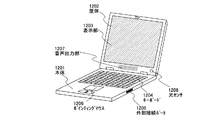
図21はコンピュータであり、本体1201、筐体1202、表示部1203、キーボード1204、外部接続ポート1205、ポインティングマウス1206、光センサ1208を含んでいる。本発明によって、強い外光下でも視認性の高いコンピュータを構成することができ、ユーザーにとって使いやすく、目の疲労を少なくすることもできる。
FIG. 21 illustrates a computer, which includes a
(実施の形態11)
図22は、本発明に係る車両の態様を示している。この車両は、外光強度を検出するセンサと、外光強度が高いときには低階調の表示を行い、外光強度が低いときには高階調の表示を行い、外光強度が両者の間にあるときにはその中間階調の表示を行う表示装置が含まれている。
(Embodiment 11)
FIG. 22 shows an aspect of the vehicle according to the present invention. This vehicle has a sensor that detects the external light intensity, and displays a low gradation when the external light intensity is high, displays a high gradation when the external light intensity is low, and when the external light intensity is between them. A display device for displaying the intermediate gradation is included.
図22(A)は当該車両の運転席を示し、図22(B)は上面から見た状態を示している。表示パネル1103は、コンソールパネル1105であって、ハンドル1102の右手に設けられている(左ハンドルのときは左手)。表示パネル1103の大きさに限定はないが、運転者の視野を妨げず、かつ、有効に情報を表示する大きさとして、縦長3.5インチパネルなどが好ましい態様となる。表示パネル1103は、運転者に向かって5度から30度の角度を付けて斜めに配置されていても良い。このような表示パネル1103は、実施の形態8で示した図9のものとすることが好ましい。
FIG. 22A shows the driver's seat of the vehicle, and FIG. 22B shows the state viewed from the top. The
この表示パネル1103は、コンソールパネル1105の一カ所又は複数箇所に設けられた光センサ1104によって外光強度を検出する。制御装置1106はその外光強度に応じて、表示パネル1103の表示階調数を制御する。この表示パネル1103には地図、渋滞情報、天気予報など運転者にとって有益な情報を表示することができる。すなわち、GPSシステムと組み合わせてナビゲーションシステムを構築することができる。この場合、車両1101の室内に直射日光が差し込んで、特に表示パネル1103に日光が当たっているような状況でも、実施の形態1で説明したように、表示パネル1103に映し出される情報を視認することができる。
The
(付記)
以上説明したように、本発明によれば以下の態様を導くことができる。
(Appendix)
As described above, according to the present invention, the following modes can be derived.
表示部と、表示部に映像信号を供給するコントローラと、外光を受光してその外光強度に応じた信号を出力する光センサとを有し、コントローラは、映像信号の階調数を変化させる階調変換部と、光センサの出力に応じて表示パネルへ出力する階調数を選択する階調出力選択部とを含んでいる表示装置。 A display unit; a controller that supplies a video signal to the display unit; and an optical sensor that receives external light and outputs a signal corresponding to the external light intensity. The controller changes the number of gradations of the video signal. And a gradation output selection unit that selects the number of gradations to be output to the display panel according to the output of the optical sensor.
表示部と、表示部に映像信号を供給するコントローラと、外光を受光してその外光強度に応じた信号を出力する光センサとを有し、コントローラは、映像信号の階調数を変化させる階調変換部と、光センサの出力に応じて表示パネルへ出力する階調数を選択する階調出力選択部とを含み、外光強度が高いときには低階調の表示を行い、外光強度が低いときには高階調の表示を行い、外光強度が両者の間にあるときにはその中間階調の表示を行う表示装置。 A display unit; a controller that supplies a video signal to the display unit; and an optical sensor that receives external light and outputs a signal corresponding to the external light intensity. The controller changes the number of gradations of the video signal. And a gradation output selection unit that selects the number of gradations to be output to the display panel in accordance with the output of the optical sensor. A display device that displays a high gradation when the intensity is low and displays an intermediate gradation when the external light intensity is between them.
表示部と、表示部に映像信号を供給するコントローラと、映像信号を記憶するメモリ部と、外光を受光してその外光強度に応じた信号を出力する光センサとを有し、コントローラは、映像信号の階調数を変化させ前記メモリ部に記憶させる階調変換部と、光センサの出力に応じて表示パネルへ出力する映像信号を前記メモリ部から読み出して表示部に送信する階調出力選択部とを含んでいる表示装置。 A display unit; a controller that supplies a video signal to the display unit; a memory unit that stores the video signal; and an optical sensor that receives external light and outputs a signal corresponding to the external light intensity. A gradation conversion unit that changes the number of gradations of the video signal and stores it in the memory unit, and a gradation that reads out the video signal output to the display panel in accordance with the output of the optical sensor from the memory unit and transmits it to the display unit A display device including an output selection unit.
表示部と、表示部に映像信号を供給するコントローラと、映像信号を記憶するメモリ部と、外光を受光してその外光強度に応じた信号を出力する光センサとを有し、コントローラは、映像信号の階調数を変化させメモリ部に記憶させる階調変換部と、光センサの出力に応じて表示パネルへ出力する映像信号を前記メモリ部から読み出して表示部に送信する階調出力選択部とを含み、外光強度が高いときには低階調の表示を行い、外光強度が低いときには高階調の表示を行い、外光強度が両者の間にあるときにはその中間階調の表示を行う表示装置。 A display unit; a controller that supplies a video signal to the display unit; a memory unit that stores the video signal; and an optical sensor that receives external light and outputs a signal corresponding to the external light intensity. A gradation converter for changing the number of gradations of the video signal and storing it in the memory unit; and a gradation output for reading out the video signal to be output to the display panel according to the output of the optical sensor from the memory unit and transmitting it to the display unit A low gradation display when the external light intensity is high, a high gradation display when the external light intensity is low, and an intermediate gradation display when the external light intensity is between them. Display device to perform.
表示部と、表示部に映像信号を供給するコントローラと、外光を受光してその外光強度に応じた信号を出力する光センサとを有し、光センサの出力に応じて、外光強度が高いときには低階調の表示を行い、外光強度が低いときには高階調の表示を行い、外光強度が両者の間にあるときにはその中間階調の表示を行う表示装置の駆動方法。 A display unit; a controller that supplies a video signal to the display unit; and an optical sensor that receives external light and outputs a signal corresponding to the external light intensity. A display device driving method in which low gradation display is performed when the light intensity is high, high gradation display is performed when the external light intensity is low, and intermediate gradation display is performed when the external light intensity is between them.
表示部と、表示部に映像信号を供給するコントローラと、外光を受光してその外光強度に応じた信号を出力する光センサとを有し、映像信号に応じて、テキスト表示、静止画表示、動画表示の各表示モードを切り替えると共に、光センサの出力に応じて、外光強度が高いときには低階調の表示を行い、外光強度が低いときには高階調の表示を行い、外光強度が両者の間にあるときにはその中間階調の表示を行う表示装置の駆動方法。 A display unit; a controller that supplies a video signal to the display unit; and an optical sensor that receives external light and outputs a signal corresponding to the external light intensity. The display mode is switched between display and moving image display, and according to the output of the light sensor, low gradation display is performed when the external light intensity is high, and high gradation display is performed when the external light intensity is low. A driving method of a display device that displays an intermediate gray level when is between them.
表示部と、表示部に映像信号を供給するコントローラと、外光を受光してその外光強度に応じた信号を出力する光センサとを有し、映像信号に応じて、テキスト表示、静止画表示、動画表示の各表示モードを切り替えると共に、光センサの出力に応じて、テキスト表示モードでは2階調から8階調の表示を行い、色数の少ない画像の表示を行うピクチャー表示モードでは4階調から16階調の表示を行い、動画を含む色数の多い自然画の表示を行う映像モードでは64階調から1024階調の表示を行うように切り替えて表示を行う表示装置の駆動方法。
A display unit; a controller that supplies a video signal to the display unit; and an optical sensor that receives external light and outputs a signal corresponding to the external light intensity. The display mode is switched between the display mode and the moving image display, and according to the output of the optical sensor, the text display mode displays from 2 to 8 gradations, and the picture
表示部と、表示部に映像信号を供給するコントローラと、外光を受光してその外光強度に応じた信号を出力する光センサとを有し、映像信号に応じて、テキスト表示、静止画表示、動画表示の各表示モードを切り替えると共に、光センサの出力に応じて、外光強度が100,000ルクスのときに2階調の表示を行い、外光強度が10,000ルクスから100,000ルクスのときに2階調から8階調の表示を行い、外光強度が1,000ルクスから10,000ルクスのときに4階調から16階調の表示を行い、外光強度が100ルクスから1,000ルクスのときに16階調から64階調の表示を行い、外光強度が100ルクス未満のときに64階調から1024階調の表示を行う表示装置の駆動方法。 A display unit; a controller that supplies a video signal to the display unit; and an optical sensor that receives external light and outputs a signal corresponding to the external light intensity. The display mode is switched between the display mode and the moving image display, and according to the output of the optical sensor, when the external light intensity is 100,000 lux, two gradations are displayed, and the external light intensity is from 10,000 lux to 100,000. Display from 2 to 8 gradations at 000 lux, display from 4 to 16 gradations when the external light intensity is from 1,000 lux to 10,000 lux, and an external light intensity of 100 A driving method of a display device that performs display from 16 gradations to 64 gradations when lux is 1,000 lux, and displays from 64 gradations to 1024 gradations when the external light intensity is less than 100 lux.
この表示装置の駆動方法において、光センサは、外光を受光して、晴天昼太陽光下の強い外光強度において、蛍光灯照明屋内の外光強度と比較して低い階調で文字情報、静止画像を表示するものが含まれる。 In this driving method of the display device, the optical sensor receives external light, and in strong external light intensity under sunny daylight sunlight, character information with a lower gradation than the external light intensity in a fluorescent lamp illumination indoor, Includes those that display still images.
この表示装置の駆動方法において、晴天昼太陽光下若しくは曇天昼太陽光下の環境で2階調から8階調、晴天日入1時間前太陽光下若しくは曇天日出1時間後太陽光下、又は蛍光灯照明屋内の環境で4階調から16階調の表示をするものが含まれる。
In the driving method of this display device, in an environment under sunny daylight sunlight or cloudy daylight sunlight, 2 to 8 gradations, under
1 表示パネル
2 プリント基板
3 画素部
4 第1の走査線駆動回路
5 第2の走査線駆動回路
6 信号線駆動回路
7 コントローラ
8 CPU
9 メモリ
10 電源回路
11 音声処理回路
12 送受信回路
13 フレキシブル基板
14 インターフェース
15 アンテナ用ポート
16 VRAM
17 DRAM
18 フラッシュメモリ
19 インターフェース
20 制御信号生成回路
21 デコーダ
22 レジスタ
23 演算回路
24 RAM
25 入力手段
26 マイクロフォン
27 スピーカー
28 アンテナ
29 光センサ
100 表示装置
101 コントローラ
102 メモリ
103 光センサ
104 アンプ
105 電源
106 表示パネル
201 第1の筐体
202 第2の筐体
203 表示画面
204 スピーカー
205 アンテナ
206 ヒンジ
207 キーボード
208 マイクロフォン
209 光センサ
301 スイッチングTFT
302 駆動TFT
303 発光素子
304 保持容量
S1 ソース信号線
V1 電源供給線
G1 ゲート信号線
SF1 サブフレーム
Ta1 アドレス期間
Ts1 サスティン期間
401 表示パネル
402 コントロール回路
403 スイッチ
404 第1のメモリ
405 第2のメモリ
406 映像信号選択スイッチ
407 スイッチ
501 第1の筐体
502 第2の筐体
503 第1の表示画面
504 第2の表示画面
505 第3の表示画面
506 スピーカー
507 アンテナ
508 ヒンジ
509 キーボード
510 マイクロフォン
511 バッテリー
601 透明基板
602 透明基板
603 電極
604 電極
605 電極
606 EL層
607 EL層
608 EL層
609 電極
610 カラーフィルタ
611 カラーフィルタ
612 カラーフィルタ
700 基板
701 ブロッキング層
702 半導体層
703 第1絶縁層
704 ゲート電極
705 第2絶縁層
706 第3絶縁層
707 配線
708 第1電極
709 EL層
710 第2電極
711 第4絶縁層
712 半導体層
750 TFT
751 容量部
752 発光素子
800 基板
801 駆動用TFT
802 第1の電極
803 EL層
804 第2の電極
812 絶縁膜
825 発光素子
830 p層側電極
831 p型層
832 i型層
833 n型層
834 n層側電極
838 光電変換素子
900 基板
901 ゲート線駆動回路
902 データ線駆動回路
903 対向電極
904 シール領域
905 接続端子部
906 接続端子
907 コンタクトホール
908 第1の幅広配線
909 第2の幅広配線
910 分岐配線
920 第1のICチップ
921 第2のICチップ
922 光センサチップ
923 対向基板
924 シール材
925 配線
951 下地層
952 ゲート絶縁膜
953 下層絶縁膜
954 上層絶縁膜
955 配線
956 配線
957 絶縁層
958 EL層
959 接続電極
960 配線
961 配線
1001 本体(A)
1002 本体(B)
1003 筐体
1004 操作スイッチ類
1005 マイクロフォン
1006 スピーカー
1007 回路基板
1008 表示パネル(A)
1009 表示パネル(B)
1010 蝶番
1011 信号処理回路
1050 光センサ
1201 本体
1202 筐体
1203 表示部
1204 キーボード
1205 外部接続ポート
1206 ポインティングマウス
1207 音声出力部
1208 光センサ
1101 車両
1102 ハンドル
1103 表示パネル
1104 光センサ
1105 コンソールパネル
1106 制御装置
DESCRIPTION OF
9
17 DRAM
18
25 Input means 26
302 Driving TFT
303
802
1002 Body (B)
1003
1009 Display panel (B)
1010
Claims (10)
前記コントローラは、映像信号の階調数を変化させる階調変換部と、前記光センサの出力に応じて表示パネルへ出力する階調数を選択する階調出力選択部とを含んでいること
を特徴とする表示装置。 A display unit, a controller that supplies a video signal to the display unit, and an optical sensor that receives external light and outputs a signal corresponding to the external light intensity,
The controller includes a gradation conversion unit that changes the number of gradations of the video signal, and a gradation output selection unit that selects the number of gradations to be output to the display panel according to the output of the photosensor. Characteristic display device.
前記コントローラは、映像信号の階調数を変化させる階調変換部と、前記光センサの出力に応じて表示パネルへ出力する階調数を選択する階調出力選択部とを含み、
外光強度が高いときには低階調の表示を行い、外光強度が低いときには高階調の表示を行い、外光強度が両者の間にあるときにはその中間階調の表示を行うこと
を特徴とする表示装置。 A display unit, a controller that supplies a video signal to the display unit, and an optical sensor that receives external light and outputs a signal corresponding to the external light intensity,
The controller includes a gradation conversion unit that changes the number of gradations of the video signal, and a gradation output selection unit that selects the number of gradations to be output to the display panel according to the output of the photosensor,
When external light intensity is high, low gradation display is performed, when external light intensity is low, high gradation display is performed, and when external light intensity is between them, intermediate gradation display is performed. Display device.
前記コントローラは、映像信号の階調数を変化させ前記メモリ部に記憶させる階調変換部と、
前記光センサの出力に応じて表示パネルへ出力する映像信号を前記メモリ部から読み出して表示部に送信する階調出力選択部とを含んでいること
を特徴とする表示装置。 A display unit, a controller that supplies a video signal to the display unit, a memory unit that stores the video signal, and an optical sensor that receives external light and outputs a signal corresponding to the external light intensity,
The controller includes a gradation conversion unit that changes the number of gradations of a video signal and stores the change in the memory unit;
A display device, comprising: a gradation output selection unit that reads out a video signal to be output to a display panel in accordance with an output of the optical sensor from the memory unit and transmits the video signal to the display unit.
前記コントローラは、映像信号の階調数を変化させ前記メモリ部に記憶させる階調変換部と、
前記光センサの出力に応じて表示パネルへ出力する映像信号を前記メモリ部から読み出して表示部に送信する階調出力選択部とを含み、
外光強度が高いときには低階調の表示を行い、外光強度が低いときには高階調の表示を行い、外光強度が両者の間にあるときにはその中間階調の表示を行うこと
を特徴とする表示装置。 A display unit, a controller that supplies a video signal to the display unit, a memory unit that stores the video signal, and an optical sensor that receives external light and outputs a signal corresponding to the external light intensity,
The controller includes a gradation conversion unit that changes the number of gradations of a video signal and stores the change in the memory unit;
A gradation output selection unit that reads out a video signal to be output to the display panel in accordance with the output of the photosensor from the memory unit and transmits the read signal to the display unit;
When external light intensity is high, low gradation display is performed, when external light intensity is low, high gradation display is performed, and when external light intensity is between them, intermediate gradation display is performed. Display device.
前記光センサの出力に応じて、外光強度が高いときには低階調の表示を行い、外光強度が低いときには高階調の表示を行い、外光強度が両者の間にあるときにはその中間階調の表示を行うこと
を特徴とする表示装置の駆動方法。 A display unit, a controller that supplies a video signal to the display unit, and an optical sensor that receives external light and outputs a signal corresponding to the external light intensity,
Depending on the output of the light sensor, a low gradation display is performed when the external light intensity is high, a high gradation display is performed when the external light intensity is low, and an intermediate gradation when the external light intensity is between them. A display device driving method, characterized by:
前記映像信号に応じて、テキスト表示、静止画表示、動画表示の各表示モードを切り替えると共に、
前記光センサの出力に応じて、外光強度が高いときには低階調の表示を行い、外光強度が低いときには高階調の表示を行い、外光強度が両者の間にあるときにはその中間階調の表示を行うこと
を特徴とする表示装置の駆動方法。 A display unit, a controller that supplies a video signal to the display unit, and an optical sensor that receives external light and outputs a signal corresponding to the external light intensity,
In accordance with the video signal, the display mode is switched between text display, still image display, and video display,
Depending on the output of the light sensor, a low gradation display is performed when the external light intensity is high, a high gradation display is performed when the external light intensity is low, and an intermediate gradation when the external light intensity is between them. A display device driving method, characterized by:
前記映像信号に応じて、テキスト表示、静止画表示、動画表示の各表示モードを切り替えると共に、
前記光センサの出力に応じて、テキスト表示モードでは2階調から8階調の表示を行い、
色数の少ない画像の表示を行うピクチャー表示モードでは4階調から16階調の表示を行い、動画を含む色数の多い自然画の表示を行う映像モードでは64階調から1024階調の表示を行うように切り替えて表示を行うこと
を特徴とする表示装置の駆動方法。 A display unit, a controller that supplies a video signal to the display unit, and an optical sensor that receives external light and outputs a signal corresponding to the external light intensity,
In accordance with the video signal, the display mode is switched between text display, still image display, and video display,
Depending on the output of the photosensor, the text display mode displays from 2 to 8 gradations,
In the picture display mode for displaying an image with a small number of colors, display is performed from 4 to 16 gradations, and in the video mode for displaying a natural image with a large number of colors including moving images, display is performed from 64 to 1024 gradations. A display device driving method, wherein display is performed by switching to perform the above.
前記映像信号に応じて、テキスト表示、静止画表示、動画表示の各表示モードを切り替えると共に、
前記光センサの出力に応じて、
外光強度が100,000ルクスのときに2階調の表示を行い、
外光強度が10,000ルクスから100,000ルクスのときに2階調から8階調の表示を行い、
外光強度が1,000ルクスから10,000ルクスのときに4階調から16階調の表示を行い、
外光強度が100ルクスから1,000ルクスのときに16階調から64階調の表示を行い、
外光強度が100ルクス未満のときに64階調から1024階調の表示を行うこと
を特徴とする表示装置の駆動方法。 A display unit, a controller that supplies a video signal to the display unit, and an optical sensor that receives external light and outputs a signal corresponding to the external light intensity,
In accordance with the video signal, the display mode is switched between text display, still image display, and video display,
Depending on the output of the light sensor,
When the external light intensity is 100,000 lux, display with 2 gradations,
When the external light intensity is 10,000 lux to 100,000 lux, display from 2 to 8 tones,
When the external light intensity is 1,000 lux to 10,000 lux, display from 4 to 16 tones,
When the external light intensity is 100 lux to 1,000 lux, display from 16 to 64 gradations,
A display device driving method, wherein display is performed from 64 gradations to 1024 gradations when the external light intensity is less than 100 lux.
前記光センサは、外光を受光して、晴天昼太陽光下の強い外光強度において、蛍光灯照明屋内の外光強度と比較して低い階調で文字情報、静止画像を表示することを特徴とする表示装置の駆動方法。 In any one of Claims 5 thru | or 8,
The light sensor receives external light, and displays character information and still images at a lower gradation compared to the external light intensity indoors in a fluorescent lamp illumination in a strong external light intensity under sunny daylight. A display device driving method.
前記光センサは、外光を受光して、晴天昼太陽光下若しくは曇天昼太陽光下の環境で2階調から8階調、晴天日入1時間前太陽光下若しくは曇天日出1時間後太陽光下、または蛍光灯照明屋内の環境で4階調から16階調の表示をすることを特徴とする表示装置。 In any one of Claims 5 thru | or 8,
The light sensor receives outside light, and has 2 to 8 gradations in sunny daylight or cloudy daylight, 1 hour before sunny daylight or 1 hour after cloudy daylight A display device that performs display of 4 to 16 gradations in sunlight or in an indoor environment illuminated by a fluorescent lamp.
Priority Applications (1)
| Application Number | Priority Date | Filing Date | Title |
|---|---|---|---|
| JP2006126985A JP2006337997A (en) | 2005-05-02 | 2006-04-28 | Display device |
Applications Claiming Priority (2)
| Application Number | Priority Date | Filing Date | Title |
|---|---|---|---|
| JP2005133803 | 2005-05-02 | ||
| JP2006126985A JP2006337997A (en) | 2005-05-02 | 2006-04-28 | Display device |
Related Child Applications (1)
| Application Number | Title | Priority Date | Filing Date |
|---|---|---|---|
| JP2012172589A Division JP5509273B2 (en) | 2005-05-02 | 2012-08-03 | Display device |
Publications (2)
| Publication Number | Publication Date |
|---|---|
| JP2006337997A true JP2006337997A (en) | 2006-12-14 |
| JP2006337997A5 JP2006337997A5 (en) | 2009-04-30 |
Family
ID=37558565
Family Applications (1)
| Application Number | Title | Priority Date | Filing Date |
|---|---|---|---|
| JP2006126985A Withdrawn JP2006337997A (en) | 2005-05-02 | 2006-04-28 | Display device |
Country Status (1)
| Country | Link |
|---|---|
| JP (1) | JP2006337997A (en) |
Cited By (15)
| Publication number | Priority date | Publication date | Assignee | Title |
|---|---|---|---|---|
| JP2008209883A (en) * | 2007-02-23 | 2008-09-11 | Samsung Sdi Co Ltd | Organic electroluminescence display device and its drive method |
| JP2008209881A (en) * | 2007-02-23 | 2008-09-11 | Samsung Sdi Co Ltd | Organic electroluminescence display device and its drive method |
| JP2008209882A (en) * | 2007-02-23 | 2008-09-11 | Samsung Sdi Co Ltd | Organic light emitting display device |
| JP2009042711A (en) * | 2007-08-08 | 2009-02-26 | Samsung Sdi Co Ltd | Organic electroluminescence display device and drive method thereof |
| JP2009048120A (en) * | 2007-08-22 | 2009-03-05 | Sharp Corp | Image processor and display image generation method |
| JP2009244878A (en) * | 2008-03-28 | 2009-10-22 | Denso Internatl America Inc | System for vehicular display |
| JP2009301013A (en) * | 2008-05-16 | 2009-12-24 | Canon Inc | Display device |
| JP2011075636A (en) * | 2009-09-29 | 2011-04-14 | Lg Display Co Ltd | Oled display |
| JP2012506567A (en) * | 2008-10-23 | 2012-03-15 | ケンブリッジ ディスプレイ テクノロジー リミテッド | Photosensor array |
| JP2012252353A (en) * | 2005-05-02 | 2012-12-20 | Semiconductor Energy Lab Co Ltd | Display device |
| JP2014512586A (en) * | 2011-02-25 | 2014-05-22 | アマゾン・テクノロジーズ、インコーポレイテッド | Interactive processing of multi-display devices |
| JP2015165333A (en) * | 2009-08-06 | 2015-09-17 | 株式会社半導体エネルギー研究所 | display device |
| JP2022087208A (en) * | 2008-10-16 | 2022-06-09 | 株式会社半導体エネルギー研究所 | Display device and electronic appliance |
| CN115834847A (en) * | 2021-09-17 | 2023-03-21 | 卡西欧计算机株式会社 | Projection system, projection method, and recording medium |
| JP7329105B2 (en) | 2017-03-22 | 2023-08-17 | マジック リープ, インコーポレイテッド | Depth-Based Foveated Rendering for Display Systems |
Citations (5)
| Publication number | Priority date | Publication date | Assignee | Title |
|---|---|---|---|---|
| JP2002175026A (en) * | 2000-12-07 | 2002-06-21 | Sony Corp | Active matrix type display device and portable terminal using the same |
| JP2002258807A (en) * | 2001-03-01 | 2002-09-11 | Matsushita Electric Ind Co Ltd | Liquid crystal display and its drive method, and information display device |
| JP2003036057A (en) * | 2001-07-23 | 2003-02-07 | Toshiba Corp | Display device |
| JP2003279930A (en) * | 2002-03-25 | 2003-10-02 | Kawasaki Microelectronics Kk | Method for driving simple matrix liquid crystal, and liquid crystal display device |
| JP2005024608A (en) * | 2003-06-30 | 2005-01-27 | Matsushita Electric Ind Co Ltd | Display device |
-
2006
- 2006-04-28 JP JP2006126985A patent/JP2006337997A/en not_active Withdrawn
Patent Citations (5)
| Publication number | Priority date | Publication date | Assignee | Title |
|---|---|---|---|---|
| JP2002175026A (en) * | 2000-12-07 | 2002-06-21 | Sony Corp | Active matrix type display device and portable terminal using the same |
| JP2002258807A (en) * | 2001-03-01 | 2002-09-11 | Matsushita Electric Ind Co Ltd | Liquid crystal display and its drive method, and information display device |
| JP2003036057A (en) * | 2001-07-23 | 2003-02-07 | Toshiba Corp | Display device |
| JP2003279930A (en) * | 2002-03-25 | 2003-10-02 | Kawasaki Microelectronics Kk | Method for driving simple matrix liquid crystal, and liquid crystal display device |
| JP2005024608A (en) * | 2003-06-30 | 2005-01-27 | Matsushita Electric Ind Co Ltd | Display device |
Cited By (21)
| Publication number | Priority date | Publication date | Assignee | Title |
|---|---|---|---|---|
| JP2012252353A (en) * | 2005-05-02 | 2012-12-20 | Semiconductor Energy Lab Co Ltd | Display device |
| US8059069B2 (en) | 2007-02-23 | 2011-11-15 | Samsung Mobile Display Co., Ltd. | Organic light emitting diode display device and driving method thereof |
| JP2008209881A (en) * | 2007-02-23 | 2008-09-11 | Samsung Sdi Co Ltd | Organic electroluminescence display device and its drive method |
| JP2008209882A (en) * | 2007-02-23 | 2008-09-11 | Samsung Sdi Co Ltd | Organic light emitting display device |
| US8305370B2 (en) | 2007-02-23 | 2012-11-06 | Samsung Display Co., Ltd. | Organic light emitting display, controller therefor and associated methods |
| JP2008209883A (en) * | 2007-02-23 | 2008-09-11 | Samsung Sdi Co Ltd | Organic electroluminescence display device and its drive method |
| US8059073B2 (en) | 2007-02-23 | 2011-11-15 | Samsung Mobile Display Co., Ltd. | Organic light emitting diode display and driving method thereof |
| JP2009042711A (en) * | 2007-08-08 | 2009-02-26 | Samsung Sdi Co Ltd | Organic electroluminescence display device and drive method thereof |
| US8427399B2 (en) | 2007-08-08 | 2013-04-23 | Samsung Display Co., Ltd. | Organic light emitting display device including signal processor for modifying image data and driving method thereof |
| JP2009048120A (en) * | 2007-08-22 | 2009-03-05 | Sharp Corp | Image processor and display image generation method |
| JP2009244878A (en) * | 2008-03-28 | 2009-10-22 | Denso Internatl America Inc | System for vehicular display |
| JP2009301013A (en) * | 2008-05-16 | 2009-12-24 | Canon Inc | Display device |
| US11930668B2 (en) | 2008-10-16 | 2024-03-12 | Semiconductor Energy Laboratory Co., Ltd. | Flexible light-emitting device and EL module including transparent conductive film |
| JP2022087208A (en) * | 2008-10-16 | 2022-06-09 | 株式会社半導体エネルギー研究所 | Display device and electronic appliance |
| JP2012506567A (en) * | 2008-10-23 | 2012-03-15 | ケンブリッジ ディスプレイ テクノロジー リミテッド | Photosensor array |
| JP2015165333A (en) * | 2009-08-06 | 2015-09-17 | 株式会社半導体エネルギー研究所 | display device |
| US9153181B2 (en) | 2009-08-06 | 2015-10-06 | Semiconductor Energy Laboratory Co., Ltd. | Electronic book using grayscale inversion for image signal correction |
| JP2011075636A (en) * | 2009-09-29 | 2011-04-14 | Lg Display Co Ltd | Oled display |
| JP2014512586A (en) * | 2011-02-25 | 2014-05-22 | アマゾン・テクノロジーズ、インコーポレイテッド | Interactive processing of multi-display devices |
| JP7329105B2 (en) | 2017-03-22 | 2023-08-17 | マジック リープ, インコーポレイテッド | Depth-Based Foveated Rendering for Display Systems |
| CN115834847A (en) * | 2021-09-17 | 2023-03-21 | 卡西欧计算机株式会社 | Projection system, projection method, and recording medium |
Similar Documents
| Publication | Publication Date | Title |
|---|---|---|
| JP5509273B2 (en) | Display device | |
| JP2006337997A (en) | Display device | |
| US20230282679A1 (en) | Display Device And Electronic Device | |
| US7636078B2 (en) | Display device and electronic device | |
| US8059109B2 (en) | Display device and electronic apparatus | |
| TWI444952B (en) | Display device | |
| TWI539423B (en) | Display device, driving method of display device, and electronic appliance | |
| JP2010103128A (en) | Electronic equipment | |
| JP4477400B2 (en) | LIGHT EMITTING DEVICE AND ELECTRONIC DEVICE | |
| JP4943058B2 (en) | Liquid crystal display | |
| JP5386059B2 (en) | Display device | |
| JP4954579B2 (en) | Driving method of display device | |
| JP5386060B2 (en) | Display device | |
| JP2007202389A (en) | Charge pump circuit and semiconductor device comprising it | |
| JP5759661B2 (en) | Display device | |
| JP5057695B2 (en) | Data latch circuit and semiconductor device | |
| US20060279561A1 (en) | Display device |
Legal Events
| Date | Code | Title | Description |
|---|---|---|---|
| A521 | Written amendment |
Free format text: JAPANESE INTERMEDIATE CODE: A523 Effective date: 20090317 |
|
| A621 | Written request for application examination |
Free format text: JAPANESE INTERMEDIATE CODE: A621 Effective date: 20090317 |
|
| A131 | Notification of reasons for refusal |
Free format text: JAPANESE INTERMEDIATE CODE: A131 Effective date: 20111220 |
|
| A521 | Written amendment |
Free format text: JAPANESE INTERMEDIATE CODE: A523 Effective date: 20120111 |
|
| A02 | Decision of refusal |
Free format text: JAPANESE INTERMEDIATE CODE: A02 Effective date: 20120612 |
|
| A521 | Written amendment |
Free format text: JAPANESE INTERMEDIATE CODE: A523 Effective date: 20120803 |
|
| A761 | Written withdrawal of application |
Free format text: JAPANESE INTERMEDIATE CODE: A761 Effective date: 20120808 |