JP2006308483A - Multilayer film and method for manufacturing multilayer film - Google Patents
Multilayer film and method for manufacturing multilayer film Download PDFInfo
- Publication number
- JP2006308483A JP2006308483A JP2005132963A JP2005132963A JP2006308483A JP 2006308483 A JP2006308483 A JP 2006308483A JP 2005132963 A JP2005132963 A JP 2005132963A JP 2005132963 A JP2005132963 A JP 2005132963A JP 2006308483 A JP2006308483 A JP 2006308483A
- Authority
- JP
- Japan
- Prior art keywords
- layer
- multilayer film
- multilayer
- film
- soft
- Prior art date
- Legal status (The legal status is an assumption and is not a legal conclusion. Google has not performed a legal analysis and makes no representation as to the accuracy of the status listed.)
- Pending
Links
Images


Abstract
Description
本発明は多層膜及び多層膜の製造方法に関し、特に軟X線の反射鏡として用いられる多層膜及び多層膜の製造方法に関するものである。 The present invention relates to a multilayer film and a multilayer film manufacturing method, and more particularly to a multilayer film used as a soft X-ray reflecting mirror and a multilayer film manufacturing method.
軟X線波長域(11〜14nm)の光に対しては、物質の屈折率は、n=1−δ−iβ(δ、β:正の実数)と表され、δ、βともに1に比べて非常に小さい(屈折率の虚部βはX線の吸収を表す)。
従って、屈折率がほぼ1に近くなりX線はほとんど屈折せず、また、必ずX線を吸収する。そのため、可視光領域の光のように屈折を利用したレンズはX線波長域の光には使用できない。そこで、反射を利用した光学系が用いられるが、やはり屈折率が1に近いために反射率は非常に低く、大部分のX線は透過するか或いは吸収されてしまう。
以上の問題を解決するために、使用するX線の波長域での屈折率と真空の屈折率(=1)との差が大きい物質と、差の小さい物質とを交互に何層も積層することでそれらの界面である反射面を多数設け、それぞれの界面からの反射波の位相が一致するように光学的干渉理論に基づいて各層の厚さを調整した多層膜による反射鏡が開発された。
For light in the soft X-ray wavelength region (11 to 14 nm), the refractive index of the substance is expressed as n = 1−δ−iβ (δ, β: positive real number), and both δ and β are compared to 1. (The imaginary part β of the refractive index represents X-ray absorption).
Therefore, the refractive index is close to 1, and X-rays are hardly refracted, and X-rays are always absorbed. Therefore, a lens using refraction like light in the visible light region cannot be used for light in the X-ray wavelength region. Therefore, an optical system using reflection is used. However, since the refractive index is close to 1, the reflectance is very low, and most X-rays are transmitted or absorbed.
In order to solve the above problems, a material having a large difference between the refractive index in the wavelength region of the X-ray to be used and a refractive index of vacuum (= 1) and a material having a small difference are stacked alternately. In this way, a multi-layer reflector was developed in which a large number of reflecting surfaces were provided as the interfaces, and the thickness of each layer was adjusted based on the optical interference theory so that the phases of the reflected waves from each interface would match. .
このような多層膜反射鏡の代表的なものとして、W(タングステン)/C(炭素)、あるいはMo(モリブデン)/Si(シリコン)等の組み合わせが知られている。そして、これらの多層膜はスパッタリング、真空蒸着、CVD等の薄膜形成技術によって作製されていた。
最近においては軟X線多層膜反射鏡の開発が進むに従い、多層膜の評価が行われるようになり、いくつかの材料の組み合わせについてその実用性が明らかにされつつある。例えば、前記Mo/Siの組み合わせの多層膜は、123Åというシリコンの吸収端の長波長側で高い反射率を示すため、軟X線縮小投影露光装置の反射光学系に用いる多層膜反射鏡として優れている。しかし、SiとMoは反応しやすいために、Mo/Si界面においてモリブデンシリサイドを形成し、反射率の低下を招いていた(モリブデンシリサイド形成については、D.G.Sterns et.al.,J.Appl.Phys.67(1990)2415.参照)。
As a representative example of such a multilayer film reflecting mirror, a combination of W (tungsten) / C (carbon), Mo (molybdenum) / Si (silicon), or the like is known. And these multilayer films were produced by thin film formation techniques, such as sputtering, vacuum evaporation, and CVD.
Recently, as the development of soft X-ray multilayer mirrors progresses, multilayer films have been evaluated, and the practicality of some combinations of materials is being clarified. For example, the multilayer film of the Mo / Si combination exhibits a high reflectance on the long wavelength side of the silicon absorption edge of 123 mm, and is therefore excellent as a multilayer film reflector used in the reflection optical system of a soft X-ray reduction projection exposure apparatus. ing. However, since Si and Mo easily react with each other, molybdenum silicide was formed at the Mo / Si interface, resulting in a decrease in reflectance (for the formation of molybdenum silicide, see DG Sterns et. Al., J. MoI. Appl. Phys. 67 (1990) 2415.).
このため、界面における反応及び拡散を防止してX線反射率を向上させる目的で、多層膜を形成している互いに屈折率の異なる物質からなるA層とB層の間に拡散防止のための中間層C層を設けた多層膜反射鏡が提案された。
以上のような中間層を設けた多層膜反射鏡としては、例えば、特許文献1では中間層として炭化ホウ素(B4C)層を設けた多層膜反射鏡が提案されている。また、特許文献2では中間層として、ホウ化物、炭化物、ケイ化物、窒化物/Be等を設けた多層膜反射鏡が、また、特許文献3ではSiO2を設けた多層膜反射鏡が提案されている。
As a multilayer film reflector provided with the above intermediate layer, for example, Patent Document 1 proposes a multilayer film reflector provided with a boron carbide (B 4 C) layer as an intermediate layer. Patent Document 2 proposes a multilayer film reflector provided with boride, carbide, silicide, nitride / Be, etc. as an intermediate layer, and
上記従来例のMo/Siの組合せによる軟X線用多層膜ミラーでは、Mo約3nm、Si約4nmを交互に積層することで、波長約13.5nmにおいて高反射率が得られる。
ところで、上記従来例で述べたように界面拡散、反応を防ぐために中間層を挿入すると、中間層によって多層膜の膜厚が厚くなる。したがって、所望の膜厚を得るためにはMo、Siの膜厚は中間層の分だけ薄く成膜しなければならない。
しかしながら、Moは膜厚約2nmで非結晶−結晶転移点を持つ(Sasa Bajt et.al:JOURNAL OF APPLIED PHYSICS ,Vol.90 No.2 [2001]参照)。そのため、Mo/Si軟X線用多層膜ミラーに上記したように界面拡散、反応を防ぐために中間層を挿入し、所望の膜厚を得るために膜厚を薄くした場合、Moが薄くなりすぎて結晶化し難くなるという点に問題があった。すなわち、Moは結晶化することで密度が増し、Siとの屈折率差が広がり高反射率化につながることから、結晶状態にある方が望ましい。
In the multilayer mirror for soft X-rays using the Mo / Si combination of the above-mentioned conventional example, high reflectance can be obtained at a wavelength of about 13.5 nm by alternately laminating about 3 nm of Mo and about 4 nm of Si.
By the way, when an intermediate layer is inserted in order to prevent interfacial diffusion and reaction as described in the conventional example, the thickness of the multilayer film is increased by the intermediate layer. Therefore, in order to obtain a desired film thickness, the film thickness of Mo and Si must be made as thin as the intermediate layer.
However, Mo has a film thickness of about 2 nm and an amorphous-crystal transition point (see Sasa Bajt et.al: JOURNAL OF APPLIED PHYSICS, Vol. 90 No. 2 [2001]). Therefore, if an intermediate layer is inserted into the Mo / Si soft X-ray multilayer mirror to prevent interfacial diffusion and reaction as described above, and the film thickness is reduced to obtain the desired film thickness, Mo becomes too thin. There was a problem in that it became difficult to crystallize. In other words, Mo is crystallized, since its density increases and the refractive index difference with Si widens, leading to high reflectivity.
本発明は、上記課題に鑑み、Si層とMo層を繰り返し積層して構成された多層膜において、これらSi層とMo層との間に中間層を設けた場合においても、所望の膜厚のもとで高い反射率を得ることが可能となる多層膜及び多層膜の製造方法を提供することを目的とするものである。 In the present invention, in view of the above problems, a multilayer film configured by repeatedly laminating a Si layer and a Mo layer has a desired film thickness even when an intermediate layer is provided between the Si layer and the Mo layer. An object of the present invention is to provide a multilayer film and a method for manufacturing the multilayer film that can obtain high reflectivity.
本発明は、上記課題を達成するために、以下のように構成した多層膜及び多層膜の製造方法を提供するものである。
すなわち、本発明の多層膜は、Si層とMo層を繰り返し積層し、これらSi層とMo層との間に中間層を設けた多層膜において、前記Mo層が、結晶化したMo層で構成されていることを特徴としている。
また、本発明の多層膜の製造方法は、SiとMoからなる材料層を繰り返し積層するに際し、これらSi層とMo層との間に中間層を設けるようにした多層膜の製造方法において、前記Mo層を所望の厚さに成膜し結晶化した後、該Mo層を所望の膜厚にエッチングする工程を有することを特徴としている。
In order to achieve the above object, the present invention provides a multilayer film and a method for producing the multilayer film configured as follows.
That is, the multilayer film of the present invention is a multilayer film in which an Si layer and an Mo layer are repeatedly laminated, and an intermediate layer is provided between the Si layer and the Mo layer, and the Mo layer is a crystallized Mo layer. It is characterized by being.
The multilayer film production method of the present invention is the multilayer film production method in which an intermediate layer is provided between the Si layer and the Mo layer when the material layers composed of Si and Mo are repeatedly laminated. The Mo layer is formed to a desired thickness and crystallized, and then the Mo layer is etched to a desired thickness.
本発明によれば、Si層とMo層を繰り返し積層して構成された多層膜において、これらSi層とMo層との間に中間層を設けた場合においても、所望の膜厚のもとで高い反射率を得ることが可能となる多層膜及び多層膜の製造方法を実現することができる。 According to the present invention, in a multilayer film configured by repeatedly laminating a Si layer and a Mo layer, even when an intermediate layer is provided between the Si layer and the Mo layer, the desired film thickness can be obtained. It is possible to realize a multilayer film and a method for manufacturing the multilayer film that can obtain a high reflectance.
本発明は、上記構成により本発明の課題を達成することができるが、その実施の形態として、具体的にはつぎのように軟X線用多層膜反射鏡Aを形成することができる。
まず、本実施の形態による軟X線用多層膜反射鏡Aを作成する前に、所望の膜構成、周期長を有する軟X線用多層膜反射鏡を形成すべく、中間層による膜厚の増加分を考慮してMo層の層厚を薄くしてMoが結晶化されていない状態のもとで、Si/中間層/Mo/中間層成膜の順に工程を踏み、これを複数回繰り返り返して軟X線用多層膜反射鏡A’を作成した。その際、所望の膜構成、周期長の多層膜を得るためには、周期長等を測定してそれらの評価を行いながら多層膜を作成する。このような軟X線用多層膜反射鏡中の一周期分の膜厚である周期長を調べる手段として、一般的に小角X線回折測定法が用いられる。この測定法によれば、軟X線用多層膜に対する小角X線回折測定によって、周期長を反映したブラッグ反射ピークを観測し、そのピーク間隔より周期長を算出することができる。
The present invention can achieve the object of the present invention with the above-described configuration. Specifically, as an embodiment thereof, the multilayer mirror A for soft X-rays can be formed as follows.
First, before forming the multilayer film reflector A for soft X-rays according to this embodiment, in order to form a multilayer film reflector for soft X-rays having a desired film configuration and periodic length, the film thickness of the intermediate layer Taking the increase into account, the Mo layer is thinned and the Mo is not crystallized, and the steps are taken in the order of Si / intermediate layer / Mo / intermediate layer formation, and this is repeated several times. Returning, soft X-ray multilayer reflector A ′ was created. At that time, in order to obtain a multilayer film having a desired film configuration and a periodic length, the multilayer film is formed while measuring the periodic length and evaluating them. A small-angle X-ray diffraction measurement method is generally used as means for examining the period length, which is the film thickness for one period, in such a soft X-ray multilayer mirror. According to this measurement method, the Bragg reflection peak reflecting the period length is observed by small-angle X-ray diffraction measurement on the multilayer film for soft X-rays, and the period length can be calculated from the peak interval.
つぎに、本実施の形態による軟X線用多層膜反射鏡Aを以下のように形成する。
上記軟X線用多層膜反射鏡A’と同一の周期長のSi/中間層/Mo/中間層による多層膜を形成するに当たり、Mo層の形成に際して膜厚が2.5nm〜5nmになるまでMo層の成膜時間を延長し、Moが十分結晶化した後に、所望の膜厚までエッチングを行う。すなわち、上記軟X線用多層膜反射鏡A’での中間層による膜厚の増加分を考慮して薄くしたMo層と同様の膜厚までエッチングを行い、上記軟X線用多層膜反射鏡A’と周期長及びMo層の膜厚が同じ膜構成のものを作成する。
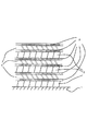
このような、Si成膜/中間層成膜/Mo成膜/エッチング/中間層成膜の順に工程を踏み、これを複数回繰り返すことによって、図1に示す軟X線用多層膜反射鏡Aを製造する。図1において、1は基板、2はSi層、3は中間層、4はMo層である。
Next, the multilayer reflector A for soft X-rays according to the present embodiment is formed as follows.
In forming a multilayer film of Si / intermediate layer / Mo / intermediate layer having the same period length as the multilayer mirror A ′ for soft X-rays, until the film thickness reaches 2.5 nm to 5 nm when forming the Mo layer After the Mo layer deposition time is extended and Mo is sufficiently crystallized, etching is performed to a desired thickness. That is, the multilayer film reflector for soft X-rays is etched to the same film thickness as that of the thin Mo layer in consideration of the increase in film thickness due to the intermediate layer in the multilayer mirror for soft X-rays A ′. A film having the same period length and the same film thickness as the Mo layer is prepared.
The steps of the Si film formation / intermediate layer film formation / Mo film formation / etching / intermediate layer film formation step are repeated in this order, and this process is repeated a plurality of times, whereby the soft X-ray multilayer reflector A shown in FIG. Manufacturing. In FIG. 1, 1 is a substrate, 2 is a Si layer, 3 is an intermediate layer, and 4 is a Mo layer.
以上の本実施の形態による軟X線用多層膜反射鏡Aによれば、Mo層は一度結晶化した後に所望の膜厚までエッチングされたものであることから、結晶化しており、Moの密度は向上したものとなっている。そのため、上記軟X線用多層膜反射鏡A’と同様の周期長及びMo層の膜厚を備える一方、Siに対する屈折率差を広げることができ、高い反射率、バンド幅を得ることが可能となる。
なお、ここで中間層の材料としては、炭化物、ホウ化物、窒化物、酸化物等の安定な材料のうち、光学特性を考慮して高い反射率が得られる材料を選択することが望ましい。
また、上記エッチングに際しては、イオンビームを用いることにより真空装置内で成膜工程と連続的に処理を行うことができる。
また、エッチングイオンビームに不活性ガスを用いることによって、エッチングによる表面粗さの増大を抑制し、散乱による反射率の低下を防ぐことができる。
According to the multilayer reflector A for soft X-rays according to the above-described embodiment, the Mo layer is crystallized because it has been crystallized once and then etched to a desired film thickness. Is an improvement. Therefore, while having the same periodic length and Mo layer thickness as the above-mentioned soft X-ray multilayer mirror A ′, it is possible to widen the refractive index difference with respect to Si, and to obtain a high reflectance and bandwidth. It becomes.
Here, as a material for the intermediate layer, it is desirable to select a material that can obtain a high reflectance in consideration of optical characteristics among stable materials such as carbide, boride, nitride, and oxide.
In the etching, an ion beam can be used to perform the process continuously with the film forming process in a vacuum apparatus.
Further, by using an inert gas for the etching ion beam, an increase in surface roughness due to etching can be suppressed, and a decrease in reflectance due to scattering can be prevented.
つぎに、本発明の実施例について説明する。本実施例においては、本発明を適用し、Arガスをイオン種とするイオンビームスパッタ装置を用いて軟X線用多層膜反射鏡aを作製した。
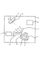
図2及び図4に本実施例で用いたイオンビームスパッタ装置の構成を示す。
図2及び図4において、5は真空チャンバー、6はエッチングイオン源、7はスパッタリングイオン源である。
8はターゲットホルダ、9は第1ターゲット、10は第2ターゲット、11は第3ターゲットである、12は成膜基板、13は成膜基板ホルダ、14はスパッタイオンビーム、15はスパッタされたターゲット粒子、16はエッチングイオンビームである。
Next, examples of the present invention will be described. In the present example, the present invention was applied, and a soft X-ray multilayer mirror “a” was produced using an ion beam sputtering apparatus using Ar gas as an ion species.
2 and 4 show the configuration of the ion beam sputtering apparatus used in this embodiment.
2 and 4, 5 is a vacuum chamber, 6 is an etching ion source, and 7 is a sputtering ion source.
8 is a target holder, 9 is a first target, 10 is a second target, 11 is a third target, 12 is a deposition substrate, 13 is a deposition substrate holder, 14 is a sputter ion beam, and 15 is a sputtered target.
まず、本実施例の軟X線用多層膜反射鏡aを作成する前に、所望の膜構成、周期長を有する軟X線用多層膜反射鏡を形成すべく、上記装置によるイオンビームにてスパッタリングによって、中間層による膜厚の増加分を考慮してMo層の層厚を薄くしてMoが結晶化されていない状態のもとで、Si(3.6nm)/B4C(0.5nm)/Mo(2.4nm)/B4C(0.5nm)の周期長を持つ軟X線用多層膜反射鏡a’を、つぎのようにして作成した。
すなわち、Arガスをイオン種とするスパッタリングイオン源7で生成されたスパッタイオンビーム14を第1ターゲット9,第2ターゲット10,第3ターゲット11に照射し、スパッタされたターゲット粒子15を放出させ、成膜基板12に堆積させて成膜するイオンビームによるスパッタリングで、Si(3.6nm)/B4C(0.5nm)/Mo(2.4nm)/B4C(0.5nm)の周期長を持つ軟X線用多層膜反射鏡a’を作成した。
図3は、この軟X線用多層膜反射鏡a’について小角X線回折測定法を用いたX線回折により、Moの結晶評価を行った結果である。
図3に示されている2θ=69°の鋭いピークは、Si基板のSi[100]によるものである。また、2θ=40°付近に緩やかなピークが観測された。これはMo[110]由来のピークである。しかし、このピークは非常に弱いことからも、ここでのMoはほとんど結晶化していないことが分かる。
First, before producing the multilayer X-ray mirror for soft X-rays of this embodiment, an ion beam by the above apparatus is used to form a multilayer X-ray mirror for soft X-rays having a desired film configuration and periodic length. In the state where Mo is not crystallized by considering the increase in film thickness due to the intermediate layer by sputtering, Si (3.6 nm) / B 4 C (0. A multilayer mirror a ′ for soft X-rays having a periodic length of 5 nm) / Mo (2.4 nm) / B 4 C (0.5 nm) was produced as follows.
That is, the
FIG. 3 shows the results of evaluation of Mo crystal by X-ray diffraction using the small-angle X-ray diffraction measurement method for the multilayer mirror a ′ for soft X-rays.
The sharp peak at 2θ = 69 ° shown in FIG. 3 is due to Si [100] of the Si substrate. In addition, a gentle peak was observed around 2θ = 40 °. This is a peak derived from Mo [110]. However, since this peak is very weak, it can be seen that Mo here is hardly crystallized.
つぎに、本実施例による軟X線用多層膜反射鏡aを以下のように形成した。
図2のようにして、上記軟X線用多層膜反射鏡a’と同一の周期長(Si(3.6nm)/B4C(0.5nm)/Mo(2.4nm)/B4C(0.5nm))の多層膜を形成するに当たり、Mo層の形成に際して膜厚が3nmになるまでMo層の成膜時間を延長し、Moが十分結晶化した後に、図4のようにArガスをイオン種とするイオンビームにてMo層の膜厚が上記軟X線用多層膜反射鏡a’と同じ膜厚の2.4nmになるまでエッチングを行った。これにより上記軟X線用多層膜反射鏡a’と周期長及びMo層の膜厚が同じ膜構成のものを作成した。
Next, the soft X-ray multilayer reflector a according to this example was formed as follows.
As shown in FIG. 2, the same periodic length (Si (3.6 nm) / B 4 C (0.5 nm) / Mo (2.4 nm) / B 4 C) as the soft X-ray multilayer reflector a ′. (0.5 nm)), when the Mo layer is formed, the film formation time of the Mo layer is extended until the film thickness reaches 3 nm. After Mo is sufficiently crystallized, Ar is formed as shown in FIG. Etching was performed with an ion beam using gas as an ion species until the thickness of the Mo layer became 2.4 nm, which is the same thickness as the multilayer mirror a ′ for soft X-rays. As a result, a film having the same film length as that of the above-mentioned multilayer mirror for soft X-ray a 'and the same period length and thickness of the Mo layer was prepared.
図5は、本実施例の多層膜反射鏡aについて小角X線回折測定法を用いたX線回折により、Moの結晶評価を行った結果である。図5に示されている2θ=69°の鋭いピークはSi基板のSi[100]によるものである。また、2θ=40°付近のMo[110]由来のピークは多層膜反射鏡Aを測定した際のピーク強度に比べ約6倍の強度を示した。
これにより、本実施例の軟X線用多層膜反射鏡aと上記軟X線用多層膜反射鏡a’とは周期長及びMo膜厚が同じであるが、本実施例のものではMo成膜時間延長後に、エッチング処理を施したことによって、Moの結晶化が促進することが確認できた。
FIG. 5 shows the results of Mo crystal evaluation by X-ray diffraction using the small-angle X-ray diffraction measurement method for the multilayer reflector a of this example. The sharp peak at 2θ = 69 ° shown in FIG. 5 is due to Si [100] of the Si substrate. Further, the peak derived from Mo [110] near 2θ = 40 ° showed an intensity about 6 times the peak intensity when the multilayer mirror A was measured.
As a result, the multilayer mirror a for soft X-rays of this embodiment and the multilayer mirror for soft X-rays a ′ have the same period length and Mo film thickness. It was confirmed that the crystallization of Mo was promoted by performing the etching treatment after extending the film time.
つぎに、本実施例の軟X線用多層膜反射鏡aと上記軟X線用多層膜反射鏡a’の軟X線分光反射率を測定したところ、本実施例の軟X線用多層膜反射鏡aの反射率は69.3%であるのに対して、上記軟X線用多層膜反射鏡a’の反射率は67.2%であった。このように、本実施例の軟X線用多層膜反射鏡aによればMoが結晶化したことによってMoの密度が向上し、Siとの屈折率差が広がったことによって反射率は2.1%増加した。
以上のように、本実施例の構成によれば、Si層とMo層を繰り返し積層して構成された多層膜において、これらSi層とMo層との間に中間層を設けた場合においても、結晶化したMo層によって、所望の膜厚のもとで高い反射率の多層膜を実現することができる。
Next, when the soft X-ray spectral reflectance of the multilayer reflector for soft X-rays of this example and the multilayer reflector for soft X-rays a ′ was measured, the multilayer film for soft X-rays of this example was measured. The reflectance of the reflecting mirror a was 69.3%, whereas the reflectance of the soft X-ray multilayer reflecting mirror a ′ was 67.2%. As described above, according to the multilayer film reflecting mirror a for soft X-rays of the present example, the Mo density is improved by crystallization of Mo, and the refractive index difference is 2. Increased by 1%.
As described above, according to the configuration of this example, in the multilayer film configured by repeatedly laminating the Si layer and the Mo layer, even when an intermediate layer is provided between the Si layer and the Mo layer, With the crystallized Mo layer, a multilayer film having a high reflectance can be realized under a desired film thickness.
1:Si[100]基板
2:Si層
3:中間層
4:Mo層
5:真空チャンバー
6:エッチングイオン源
7:スパッタリングイオン源
8:ターゲットホルダ
9:第1ターゲット
10:第2ターゲット
11:第3ターゲット
12:成膜基板
13:成膜基板ホルダ
14:スパッタイオンビーム
15:スパッタされたターゲット粒子
16:エッチングイオンビーム
1: Si [100] substrate 2: Si layer 3: Intermediate layer 4: Mo layer 5: Vacuum chamber 6: Etching ion source 7: Sputtering ion source 8: Target holder 9: First target 10: Second target 11:
Claims (8)
前記Mo層が、結晶化したMo層で構成されていることを特徴とする多層膜。 In the multilayer film in which the Si layer and the Mo layer are repeatedly laminated, and an intermediate layer is provided between the Si layer and the Mo layer,
A multilayer film characterized in that the Mo layer is composed of a crystallized Mo layer.
前記Mo層を所望の厚さに成膜し結晶化した後、該Mo層を所望の膜厚にエッチングする工程を有することを特徴とする多層膜の製造方法。 In the method of manufacturing a multilayer film in which an intermediate layer is provided between the Si layer and the Mo layer when the material layers made of Si and Mo are repeatedly laminated,
A method for producing a multilayer film, comprising: forming a Mo layer to a desired thickness and crystallizing the Mo layer, and then etching the Mo layer to a desired thickness.
Priority Applications (1)
| Application Number | Priority Date | Filing Date | Title |
|---|---|---|---|
| JP2005132963A JP2006308483A (en) | 2005-04-28 | 2005-04-28 | Multilayer film and method for manufacturing multilayer film |
Applications Claiming Priority (1)
| Application Number | Priority Date | Filing Date | Title |
|---|---|---|---|
| JP2005132963A JP2006308483A (en) | 2005-04-28 | 2005-04-28 | Multilayer film and method for manufacturing multilayer film |
Publications (2)
| Publication Number | Publication Date |
|---|---|
| JP2006308483A true JP2006308483A (en) | 2006-11-09 |
| JP2006308483A5 JP2006308483A5 (en) | 2008-06-19 |
Family
ID=37475531
Family Applications (1)
| Application Number | Title | Priority Date | Filing Date |
|---|---|---|---|
| JP2005132963A Pending JP2006308483A (en) | 2005-04-28 | 2005-04-28 | Multilayer film and method for manufacturing multilayer film |
Country Status (1)
| Country | Link |
|---|---|
| JP (1) | JP2006308483A (en) |
Cited By (3)
| Publication number | Priority date | Publication date | Assignee | Title |
|---|---|---|---|---|
| JP2010518594A (en) * | 2007-02-05 | 2010-05-27 | カール・ツァイス・エスエムティー・アーゲー | Multilayer reflective optical element for EUV lithography apparatus comprising first and second additional intermediate layers |
| DE102011090192A1 (en) | 2011-01-01 | 2012-07-05 | Canon K. K. | Mirrors, methods of making the same, exposure apparatus, and apparatus manufacturing methods |
| CN111752085A (en) * | 2019-03-27 | 2020-10-09 | Hoya株式会社 | Substrate with multilayer reflective film, reflective mask blank, reflective mask, and method for manufacturing semiconductor device |
Citations (8)
| Publication number | Priority date | Publication date | Assignee | Title |
|---|---|---|---|---|
| JPH0253001A (en) * | 1988-08-17 | 1990-02-22 | Canon Inc | Production of multilayer film for soft x-rays and vacuum ultraviolet rays |
| JPH02242201A (en) * | 1989-03-16 | 1990-09-26 | Canon Inc | Multilayered film reflecting mirror for soft x-ray and vacuum ultraviolet ray |
| JPH03274001A (en) * | 1990-03-24 | 1991-12-05 | Seiko Epson Corp | X-ray reflecting film |
| JPH06273605A (en) * | 1993-01-05 | 1994-09-30 | American Teleph & Telegr Co <Att> | Method of optical device recovery |
| JPH09230098A (en) * | 1996-02-21 | 1997-09-05 | Nippon Telegr & Teleph Corp <Ntt> | Multilayer film x-ray reflecting mirror |
| WO2001041155A1 (en) * | 1999-11-29 | 2001-06-07 | Tohoku Techno Arch Co., Ltd. | Optical element such as multilayer film reflection mirror, production method therefor and device using it |
| JP2001183499A (en) * | 1999-12-22 | 2001-07-06 | Rigaku Industrial Co | X-ray spectral element and fluorescent x-ray analyzer using the same |
| JP2004532413A (en) * | 2001-05-01 | 2004-10-21 | ザ・リージェンツ・オブ・ジ・ユニバーシティ・オブ・カリフォルニア | Extreme ultraviolet lithography (EUVL) multilayer structure |
-
2005
- 2005-04-28 JP JP2005132963A patent/JP2006308483A/en active Pending
Patent Citations (8)
| Publication number | Priority date | Publication date | Assignee | Title |
|---|---|---|---|---|
| JPH0253001A (en) * | 1988-08-17 | 1990-02-22 | Canon Inc | Production of multilayer film for soft x-rays and vacuum ultraviolet rays |
| JPH02242201A (en) * | 1989-03-16 | 1990-09-26 | Canon Inc | Multilayered film reflecting mirror for soft x-ray and vacuum ultraviolet ray |
| JPH03274001A (en) * | 1990-03-24 | 1991-12-05 | Seiko Epson Corp | X-ray reflecting film |
| JPH06273605A (en) * | 1993-01-05 | 1994-09-30 | American Teleph & Telegr Co <Att> | Method of optical device recovery |
| JPH09230098A (en) * | 1996-02-21 | 1997-09-05 | Nippon Telegr & Teleph Corp <Ntt> | Multilayer film x-ray reflecting mirror |
| WO2001041155A1 (en) * | 1999-11-29 | 2001-06-07 | Tohoku Techno Arch Co., Ltd. | Optical element such as multilayer film reflection mirror, production method therefor and device using it |
| JP2001183499A (en) * | 1999-12-22 | 2001-07-06 | Rigaku Industrial Co | X-ray spectral element and fluorescent x-ray analyzer using the same |
| JP2004532413A (en) * | 2001-05-01 | 2004-10-21 | ザ・リージェンツ・オブ・ジ・ユニバーシティ・オブ・カリフォルニア | Extreme ultraviolet lithography (EUVL) multilayer structure |
Cited By (7)
| Publication number | Priority date | Publication date | Assignee | Title |
|---|---|---|---|---|
| JP2010518594A (en) * | 2007-02-05 | 2010-05-27 | カール・ツァイス・エスエムティー・アーゲー | Multilayer reflective optical element for EUV lithography apparatus comprising first and second additional intermediate layers |
| JP2013219383A (en) * | 2007-02-05 | 2013-10-24 | Carl Zeiss Smt Gmbh | Multilayer reflective optical element for euv lithography device comprising first and second additional intermediate layers |
| TWI427334B (en) * | 2007-02-05 | 2014-02-21 | Zeiss Carl Smt Gmbh | Reflective optical element for euv lithography devices |
| DE102011090192A1 (en) | 2011-01-01 | 2012-07-05 | Canon K. K. | Mirrors, methods of making the same, exposure apparatus, and apparatus manufacturing methods |
| US9063277B2 (en) | 2011-01-01 | 2015-06-23 | Canon Kabushiki Kaisha | Mirror, method of manufacturing the same, exposure apparatus, and device manufacturing method |
| DE102011090192B4 (en) | 2011-01-01 | 2020-07-30 | Canon K. K. | Mirror, method of making the same, exposure device and device manufacturing method |
| CN111752085A (en) * | 2019-03-27 | 2020-10-09 | Hoya株式会社 | Substrate with multilayer reflective film, reflective mask blank, reflective mask, and method for manufacturing semiconductor device |
Similar Documents
| Publication | Publication Date | Title |
|---|---|---|
| US6396900B1 (en) | Multilayer films with sharp, stable interfaces for use in EUV and soft X-ray application | |
| KR101176682B1 (en) | Thermally stable multilayer mirror for the euv spectral region | |
| JP2005308722A (en) | Soft x-ray multilayered film reflection mirror, and soft x-ray reflection optical system | |
| Braun et al. | Multi component EUV multilayer mirrors | |
| JP2883100B2 (en) | Half mirror or beam splitter for soft X-ray and vacuum ultraviolet | |
| JP5258368B2 (en) | Method for manufacturing substrate with multilayer reflective film, method for manufacturing reflective mask blank, and method for manufacturing reflective mask | |
| JP2006308483A (en) | Multilayer film and method for manufacturing multilayer film | |
| JP2008026093A (en) | Multilayer film reflection mirror and method for manufacturing it | |
| JP2010280931A (en) | Multilayer film deposition process | |
| JP5916821B2 (en) | Hafnium oxide coating | |
| JP3033323B2 (en) | Method for manufacturing X-ray multilayer mirror | |
| Mao et al. | Development of grazing incidence multilayer mirrors for hard X-ray focusing telescopes | |
| JP2993261B2 (en) | X-ray multilayer reflector | |
| JP2007163191A (en) | Multilayer-film reflector and optical system equipped with multilayer-film reflector | |
| JP4343895B2 (en) | Multilayer mirror for soft X-ray | |
| JP2535038B2 (en) | Multi-layer film mirror for X-ray / VUV | |
| JP2007163221A (en) | Manufacturing method for multilayer-film reflector | |
| US20210373212A1 (en) | High reflectance and high thermal stability in reactively sputtered multilayers | |
| Wang et al. | Mo/SiO 2 multilayers for soft x-ray optical applications | |
| JP2004085975A (en) | Oxide multilayer optical element and manufacturing method therefor | |
| Gaponov et al. | Spherical and plane multilayer normal incidence mirrors for soft x-rays | |
| JPH05283322A (en) | Mask for exposure to x-ray | |
| JP2002277589A (en) | Mo/Si MULTILAYER FILM AND METHOD FOR IMPROVING ITS HEAT RESISTANCE | |
| JP3648791B2 (en) | Manufacturing method of multilayer mirror | |
| JP2535037B2 (en) | Multi-layer film mirror for X-ray / VUV |
Legal Events
| Date | Code | Title | Description |
|---|---|---|---|
| A521 | Written amendment |
Free format text: JAPANESE INTERMEDIATE CODE: A523 Effective date: 20080425 |
|
| A621 | Written request for application examination |
Free format text: JAPANESE INTERMEDIATE CODE: A621 Effective date: 20080425 |
|
| A131 | Notification of reasons for refusal |
Free format text: JAPANESE INTERMEDIATE CODE: A131 Effective date: 20100202 |
|
| A02 | Decision of refusal |
Free format text: JAPANESE INTERMEDIATE CODE: A02 Effective date: 20100531 |