JP2006303360A - Through-wire board, composite board, and electronic apparatus - Google Patents
Through-wire board, composite board, and electronic apparatus Download PDFInfo
- Publication number
- JP2006303360A JP2006303360A JP2005126244A JP2005126244A JP2006303360A JP 2006303360 A JP2006303360 A JP 2006303360A JP 2005126244 A JP2005126244 A JP 2005126244A JP 2005126244 A JP2005126244 A JP 2005126244A JP 2006303360 A JP2006303360 A JP 2006303360A
- Authority
- JP
- Japan
- Prior art keywords
- wiring
- base material
- substrate
- exposed
- board
- Prior art date
- Legal status (The legal status is an assumption and is not a legal conclusion. Google has not performed a legal analysis and makes no representation as to the accuracy of the status listed.)
- Pending
Links
Images


Classifications
-
- H—ELECTRICITY
- H01—ELECTRIC ELEMENTS
- H01L—SEMICONDUCTOR DEVICES NOT COVERED BY CLASS H10
- H01L2924/00—Indexing scheme for arrangements or methods for connecting or disconnecting semiconductor or solid-state bodies as covered by H01L24/00
- H01L2924/0001—Technical content checked by a classifier
- H01L2924/0002—Not covered by any one of groups H01L24/00, H01L24/00 and H01L2224/00
Landscapes
- Production Of Multi-Layered Print Wiring Board (AREA)
- Printing Elements For Providing Electric Connections Between Printed Circuits (AREA)
Abstract
Description
本発明は、電子デバイスや光学デバイス、MEMSデバイス等の高密度実装、またはそれらのデバイスを一つのパッケージ内でシステム化するSiP(システムインパッケージ)を可能にする貫通配線を備えた貫通配線基板や複合基板、及びこれらを用いた電子装置に関する。 The present invention relates to a through-wiring board having a through-wiring that enables high-density mounting of electronic devices, optical devices, MEMS devices, etc., or SiP (system-in-package) for systematizing these devices in one package, The present invention relates to a composite substrate and an electronic device using these.
近年、携帯電話等の電子機器の高機能化に伴い、それらに使われる電子デバイス等にも更なる高速化、高機能化が要求されている。これを実現するためには、微細化等によるデバイス自身の高速化だけではなく、デバイスのパッケージにも高速化、高密度化に向けた技術開発が必須となっている。 In recent years, with the enhancement of functions of electronic devices such as mobile phones, electronic devices and the like used for them have been required to have higher speed and higher functions. In order to realize this, not only the speed of the device itself by miniaturization and the like, but also the development of technology for the speed and density of the device package is indispensable.
高密度実装を実現する技術として、微細な貫通電極を用いてチップを積層実装する三次元実装や、貫通電極が形成された貫通配線基板を用いたSiPが提案されており、これを実現するための貫通電極形成技術や貫通配線基板の形成技術が活発に研究、開発されている。 In order to realize high-density mounting, three-dimensional mounting in which chips are stacked and mounted using fine through electrodes and SiP using a through wiring substrate on which through electrodes are formed have been proposed. The through electrode forming technology and the through wiring substrate forming technology have been actively researched and developed.
図19は、セラミックやシリコン等のリジッドな貫通配線基板を用いてなるSiP(Single in line Package)の模式的な断面図である。貫通配線基板191上に複数のデバイス195A、195Bが貫通電極193と電気的に接続するように実装されており、全体として一つのパッケージを形成している。その際、図19に示すように、従来の貫通配線基板においては、その表裏の主平面間を最短距離でつなぐように主平面に対して垂直に貫通電極が設けられていた。
FIG. 19 is a schematic cross-sectional view of a SiP (Single in line Package) using a rigid through wiring substrate such as ceramic or silicon. A plurality of devices 195 </ b> A and 195 </ b> B are mounted on the through
このような貫通電極を配してなるを貫通配線基板を用いたSiPにおいては、以下に示す技術的な問題点があった。
(1)三次元実装において、積層するデバイスが異種デバイスである場合、デバイスごとに必要な電極の数や電極のピッチが異なるため、これらの差異を解消するための表面配線や配線基板(インターポーザー)が必要になる。
(2)SiPにおいて使用される貫通配線基板においても、基板上に搭載されるデバイスの電極ピッチと、マザーボード等に実装される際のバンプピッチとに大きな差異があるため、貫通配線基板上にこれらの差異を解消するための配線形成が必要となる。
(3)貫通配線を用いた三次元的な実装とはいえ、貫通電極は基本的に基板表裏を貫通するものであるため、隣り合う貫通配線基板間を電気的に接続する際には小型化等に制約がある。
In SiP using such a through electrode and using a through wiring substrate, there are the following technical problems.
(1) In three-dimensional mounting, if the devices to be stacked are different devices, the number of electrodes required and the pitch of the electrodes differ from device to device, so surface wiring and wiring boards (interposers) to eliminate these differences ) Is required.
(2) Even in the through wiring substrate used in the SiP, there is a large difference between the electrode pitch of the device mounted on the substrate and the bump pitch when mounted on the mother board or the like. It is necessary to form a wiring for eliminating the difference.
(3) Although it is three-dimensional mounting using through wiring, since the through electrode basically penetrates the front and back of the board, it is reduced in size when electrically connecting adjacent through wiring boards. Etc. are limited.
上記問題点を解決する一例としては、所望の回路が形成されたチップ本体と、このチップ本体の表裏を貫通した複数の貫通孔にそれぞれ埋め込み形成された貫通電極とを備え、前記貫通孔が、前記チップ本体の主平面と垂直な方向に対し傾けて形成されている構成からなる半導体チップが挙げられる(特許文献1)。 As an example to solve the above problems, a chip body in which a desired circuit is formed and a through electrode embedded in a plurality of through holes penetrating the front and back of the chip body, the through hole, An example of the semiconductor chip is a structure in which the chip body is inclined with respect to a direction perpendicular to the main plane of the chip body (Patent Document 1).
上記半導体チップに採用された技術、すなわち基板を斜めに貫通する貫通電極を配線基板に応用すれば、単に基板表裏のピッチを変えることは可能となる。しかしながら、この場合においても、直線的な貫通電極であるが故に、貫通電極の位置的な制限が生じるので、電気的な接続手段となる貫通電極の露呈部はその配置が制限され、配線構造の設計自由度が低くなるため、より高密度な三次元実装を行うことは困難であった。
本発明は上記事情に鑑みてなされたもので、配線構造の設計自由度が高く、高密度な三次元実装を可能とする貫通配線を備えた貫通配線基板や複合基板、及びこれらを用いた電子装置を提供することを目的とする。 The present invention has been made in view of the above circumstances, and has a high degree of freedom in designing a wiring structure, a through wiring substrate or a composite substrate having a through wiring that enables high-density three-dimensional mounting, and an electronic device using these. An object is to provide an apparatus.
本発明の請求項1に係る貫通配線基板は、基材を構成する少なくとも二面を結ぶように微細孔を配し、該微細孔に導電性物質を充填してなる貫通配線を備えた貫通配線基板であって、前記貫通配線は、少なくとも一部に、前記基材の厚み方向とは異なる方向に延びる部分を有することを特徴とする。
本発明の請求項2に係る貫通配線基板は、請求項1において、前記貫通配線の一端は前記基材の(一方の)主面に、前記貫通配線の他端は前記基材の(何れかの)側面に、それぞれ露呈されてなることを特徴とする。
本発明の請求項3に係る貫通配線基板は、請求項1において、前記貫通配線の一端は前記基材の一方の主面に、前記貫通配線の他端は前記基材の他方の主面に、それぞれ露呈されてなることを特徴とする。
本発明の請求項4に係る貫通配線基板は、請求項1において、前記貫通配線は、前記基材内に分岐する部分を備えていることを特徴とする。
本発明の請求項5に係る貫通配線基板は、請求項1において、前記貫通配線の一端及び/又は他端は、接合する他の基板の電極に対応する位置に配されていることを特徴とする。
本発明の請求項6に係る複合基板は、請求項1乃至5のいずれか1項に記載の貫通配線基板を複数用い、互いの主面同士及び/又は側面同士を重ね合わせ、互いの貫通配線基板を構成する貫通配線を電気的に接続してなることを特徴とする。
本発明の請求項7に係る電子装置は、請求項1乃至5のいずれか1項に記載の貫通配線基板又は請求項6に記載の複合基板に電子部品を実装してなることを特徴とする。
A through wiring board according to claim 1 of the present invention is a through wiring having a through hole in which a fine hole is arranged so as to connect at least two surfaces constituting a base material, and the fine hole is filled with a conductive substance. It is a board | substrate, Comprising: The said penetration wiring has a part extended in the direction different from the thickness direction of the said base material in at least one part, It is characterized by the above-mentioned.
The through wiring board according to claim 2 of the present invention is the through wiring substrate according to claim 1, wherein one end of the through wiring is on one side of the base material, and the other end of the through wiring is on the base material. It is characterized in that it is exposed on each side surface.
The through wiring board according to claim 3 of the present invention is the through wiring board according to claim 1, wherein one end of the through wiring is on one main surface of the base material, and the other end of the through wiring is on the other main surface of the base material. , Each of which is exposed.
According to a fourth aspect of the present invention, there is provided a through wiring substrate according to the first aspect, wherein the through wiring includes a portion branched into the base material.
The through wiring board according to claim 5 of the present invention is characterized in that, in claim 1, one end and / or the other end of the through wiring is arranged at a position corresponding to an electrode of another substrate to be joined. To do.
A composite substrate according to a sixth aspect of the present invention uses a plurality of the through wiring boards according to any one of the first to fifth aspects, and superimposes the main surfaces and / or the side surfaces to each other to form the through wirings. It is characterized in that the through wiring constituting the substrate is electrically connected.
An electronic device according to a seventh aspect of the present invention is characterized in that an electronic component is mounted on the through wiring board according to any one of the first to fifth aspects or the composite substrate according to the sixth aspect. .
本発明に係る貫通配線基板(請求項1)は、基材を構成する少なくとも二面を結ぶように微細孔を配し、該微細孔に導電性物質を充填してなる貫通配線を備え、この貫通配線が、少なくとも一部に、基材の厚み方向とは異なる方向に延びる部分を有するので、貫通配線はその一端を基材の一面に、他端を基材の全ての他面に、それぞれ露呈させる構成とすることができる。つまり、貫通配線の他端を露呈させる他面は、その一端を露呈させた一面と必ずしも対向する位置にある必要はない。ゆえに、本発明によれば、貫通配線を通じて基材を構成する、あらゆる面同士の間を電気的に接続できるので、より設計の自由度が高く、高密度実装あるいは三次元実装を可能とする貫通配線基板が得られる。 A through wiring board according to the present invention (Claim 1) includes a through wiring in which fine holes are arranged so as to connect at least two surfaces constituting a base material, and the fine holes are filled with a conductive substance. Since the through wiring has at least a part extending in a direction different from the thickness direction of the base material, the through wiring has one end on one surface of the base material and the other end on all other surfaces of the base material, respectively. It can be set as the structure to expose. In other words, the other surface that exposes the other end of the through wiring does not necessarily have to be in a position facing the one surface that exposes the other end. Therefore, according to the present invention, since all surfaces constituting the base material can be electrically connected to each other through the through wiring, the design freedom is high, and the penetration enabling high-density mounting or three-dimensional mounting is possible. A wiring board is obtained.
本発明に係る複合基板(請求項6)は、上記構成とした貫通配線基板を複数用い、互いの主面同士及び/又は側面同士を重ね合わせ、互いの貫通配線基板を構成する貫通配線を電気的に接続してなる。この構成によれば、同種あるいは異種の機能を備えた貫通配線基板を必要に応じて電気的に接続させることにより、接続能力の増加や接続機能の多角化などを適宜、図ることができる複合基板の提供が可能となる。ゆえに、本発明は、三次元実装やSiPにおいて、より高機能、高密度なパッケージをもたらし、ひいてはデバイスの高速化、高機能化に貢献する。 The composite substrate according to the present invention (Claim 6) uses a plurality of through-wiring boards having the above-described configuration, and superimposes the main surfaces and / or side surfaces of each other to electrically connect the through-wirings constituting each through-wiring substrate. Connected. According to this configuration, a composite circuit board capable of appropriately increasing connection capability and diversifying connection functions by electrically connecting through wiring boards having the same or different functions as necessary. Can be provided. Therefore, the present invention provides a higher-functionality and higher-density package in three-dimensional mounting and SiP, and thus contributes to higher speed and higher functionality of the device.
本発明の請求項7に係る電子装置は、上記構成とした貫通配線基板又は複合基板に電子部品を実装してなるので、電子装置の薄型化や小型化、低消費電力化などを図ることが可能となる。 Since the electronic device according to claim 7 of the present invention is formed by mounting electronic components on the through wiring board or the composite substrate having the above-described configuration, the electronic device can be reduced in thickness, size, power consumption, and the like. It becomes possible.
以下、本発明の一実施の形態について説明する。
図1〜7は、本発明に係る貫通配線基板の一例を示す断面図である。各図面に示すように、本発明の貫通配線基板は何れも、基材を構成する少なくとも二面を結ぶように微細孔を配し、該微細孔に導電性物質を充填してなる貫通配線を備えた貫通配線基板であり、前記貫通配線は、少なくとも一部に、前記基材の厚み方向とは異なる方向に延びる部分を有するので、貫通配線はその一端を基材の一面に、他端を基材の(全ての)他面に、それぞれ露呈させる構成とすることができる。これにより、貫通配線を通じて基材を構成する、あらゆる面同士の間を電気的に接続可能となる。
具体的は、次の4つの形態が挙げられる。なお、各形態の説明において直線部と表現した貫通配線の箇所は、これ(直線状)に限定されるものではなく、例えば曲線状や屈曲状としても構わない。
Hereinafter, an embodiment of the present invention will be described.
1-7 is sectional drawing which shows an example of the penetration wiring board based on this invention. As shown in each drawing, each of the through wiring boards of the present invention has a through hole formed by arranging a fine hole so as to connect at least two surfaces constituting a base material and filling the fine hole with a conductive substance. Since the through wiring has at least a part extending in a direction different from the thickness direction of the base material, the through wiring has one end on one surface of the base material and the other end. It can be set as the structure exposed to (all) other surfaces of a base material, respectively. Thereby, it becomes possible to connect electrically between all the surfaces which comprise a base material through penetration wiring.
Specifically, there are the following four forms. In addition, the location of the through wiring expressed as a straight portion in the description of each embodiment is not limited to this (straight shape), and may be a curved shape or a bent shape, for example.
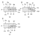
<第一の形態>
第一の形態は、貫通配線の一端が基材の主面に、貫通配線の他端が基材の側面に、それぞれ露呈されてなる構成である。
図1に示すように、例えば貫通配線13が直線状をなし、貫通配線13自体が基材11の厚み方向(紙面の上下方向)とは異なる方向に延びている例が挙げられる。
図1(a)は貫通配線13の一端13αと他端13βがそれぞれ基材の一面(紙面の上面)11aと側面11cに露呈した場合を、図1(b)は貫通配線13の一端13αと他端13βがそれぞれ基材の他面(紙面の下面)11bと側面11cに露呈した場合を、各々示している。
<First form>
In the first form, one end of the through wiring is exposed on the main surface of the base material, and the other end of the through wiring is exposed on the side surface of the base material.
As shown in FIG. 1, for example, the
1A shows a case where one end 13α and the other end 13β of the through
また図2に示すように、例えば貫通配線23が2つの直線部と1つの屈曲部との組み合わせからなり、少なくとも1つの直線部が基材21の厚み方向(紙面の上下方向)とは異なる方向に延びている例も挙げられる。
図2(a)は貫通配線23をなす2つの直線部23a、23bが屈曲部24において接続されており、直線部23aは基材21の厚み方向に延びて紙面の上面21aに露呈する一端23αを、直線部23bは基材21の厚み方向と垂直をなす方向に延びて紙面の側面21cに露呈する他端23βを有する。
図2(b)は貫通配線23をなす2つの直線部23c、23dが屈曲部24において接続されており、直線部23cは基材21の厚み方向に延びて紙面の上面21aに露呈する一端23αを、直線部23dは基材21の厚み方向と傾斜をなす方向に延びて紙面の側面21cに露呈する他端23βを有する。
図2(c)は貫通配線23をなす2つの直線部23e、23fが屈曲部24において接続されており、直線部23eは基材21の厚み方向と傾斜をなす方向に延びて紙面の下面21bに露呈する一端23αを、直線部23fは基材21の厚み方向と垂直をなす方向に延びて紙面の側面21cに露呈する他端23βを有する。
As shown in FIG. 2, for example, the
In FIG. 2A, two
In FIG. 2B, two
In FIG. 2C, two
図1(図2)に示した構成例とするためには、基材11(21)をなす一方の主面11a(21a)又は他方の主面11b(21b)と、側面11c(21c)とを結ぶように、直線部をなす微細孔12(22)を設け、この微細孔12(22)に導電性物質を充填し、貫通配線13(23)を形成すればよい。
In order to obtain the configuration example shown in FIG. 1 (FIG. 2), one
<第二の形態>
第二の形態は、図3に示すように、貫通配線の一端が基材の一方の主面に、貫通配線の他端は基材の他方の主面に、それぞれ露呈されてなる構成である。
図3に示すように、例えば貫通配線33が複数の直線部と屈曲部との組み合わせからなり、少なくとも1つの直線部が基材31の厚み方向(紙面の上下方向)とは異なる方向に延びている例が挙げられる。図3(a)〜図3(d)は貫通配線33の一端33αと他端33βがそれぞれ基材の一面(紙面の上面)31aと他面(紙面の下面)31bに露呈している状態は共通しているが、以下の点において各々特長を有する。
図3(a)の構成例では、2つの直線部33a、33bが1つの屈曲部で結合されており、一方の直線部33bのみ基材31の厚み方向(紙面の上下方向)とは異なる方向に延びている。
図3(b)の構成例では、3つの直線部33c、33d、33eが2つの屈曲部で結合されており、中間の直線部33dのみ基材31の厚み方向(紙面の上下方向)とは異なる方向に延びている。
図3(c)の構成例では、2つの直線部33f、33gが1つの屈曲部で結合されている点は図2(a)と同様であるが、両方の直線部33f、33gとも基材31の厚み方向(紙面の上下方向)とは異なる方向に延びている。
図3(d)の構成例では、図3(b)の中間に配した1つの直線部に代えて、3つの直線部と2つの屈曲部33b、33cからなる部分33jを設けた点が図3(b)と異なる。図3(d)の33h、33jは、図3(b)の33c、33eに相当するものである。
図3に示した構成例とするためには、基材31をなす一方の主面31aと他方の主面31bとを結ぶように、複数の直線部と屈曲部とを組み合わせてなる微細孔32を設け、この微細孔32に導電性物質を充填し、貫通配線33を形成すればよい。
<Second form>
As shown in FIG. 3, the second form is a configuration in which one end of the through wiring is exposed on one main surface of the base material, and the other end of the through wiring is exposed on the other main surface of the base material. .
As shown in FIG. 3, for example, the through
In the configuration example of FIG. 3A, two
In the configuration example of FIG. 3B, three
3C is the same as FIG. 2A in that the two
In the configuration example of FIG. 3D, a
In order to obtain the configuration example shown in FIG. 3, the
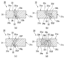
<第三の形態>
第三の形態は、図4に示すように、貫通配線の一端が基材の一方の主面に、貫通配線の他端は基材の他方の主面に、それぞれ露呈されてなる構成である。
図4に示すように、例えば貫通配線43が複数の直線部と分岐部との組み合わせからなり、少なくとも1つの直線部が基材41の厚み方向(紙面の上下方向)とは異なる方向に延びている例が挙げられる。
図4(a)〜図4(b)は分岐部から延びる貫通配線43の端部43α〜43δがそれぞれ基材の一面(紙面の上面)41aと他面(紙面の下面)41bに露呈している状態は共通しているが、以下の点において各々特長を有する。
図4(a)の構成例では、1つの分岐部44から直線部43a〜43cが個々に一面41a又は他面41bに延びている。
図4(b)の構成例では、2つの分岐部44a、44bから直線部43d〜43gが個々に一面41a又は他面41bに延びている。
図4に示した構成例とするためには、基材41をなす一方の主面41aと他方の主面41bとを結ぶように、複数の直線部と分岐部とを組み合わせてなる微細孔42を設け、この微細孔42に導電性物質を充填し、貫通配線43を形成すればよい。
<Third form>
As shown in FIG. 4, the third embodiment is configured such that one end of the through wiring is exposed on one main surface of the base material, and the other end of the through wiring is exposed on the other main surface of the base material. .
As shown in FIG. 4, for example, the through
4 (a) to 4 (b), the end portions 43α to 43δ of the through
In the configuration example of FIG. 4A,
In the configuration example of FIG. 4B, the
In order to obtain the configuration example shown in FIG. 4, the fine holes 42 formed by combining a plurality of linear portions and branch portions so as to connect one
また図5に示すように、例えば貫通配線53が直線部と屈曲部と分岐部の組み合わせからなり、少なくとも1つの直線部が基材51の厚み方向(紙面の上下方向)とは異なる方向に延びている例も挙げられる。図5(a)〜図5(c)は貫通配線53の一端または他端53α〜53δが基材の一面(紙面の上面)51a又は他面(紙面の下面)51bの何れかに露呈している状態は共通しているが、以下の点において各々特長を有する。
図5(a)の構成例では、5つの直線部53a〜53eが2つの屈曲部54b、54cと1つの分岐部54aで結合されており、分岐部54aと屈曲部54b、54cを繋ぐ直線部53b、53cのみ基材51の厚み方向(紙面の上下方向)とは異なる方向に延びている。
図5(b)の構成例では、基板の厚み方向に貫通する1つの直線部53fから分岐した複数の直線部53g、53hをもち、この2つの直線部は両方とも基材51の厚み方向(紙面の上下方向)とは異なる方向に延びている。また、一方の直線部53hは屈曲部を介して他の直線部53iに繋がっている。
図5(c)の構成例では、基板の厚み方向に貫通する1つの直線部53jから分岐した複数の直線部53k、53mをもち、この2つの直線部は両方とも基材51の厚み方向(紙面の上下方向)とは異なる方向に延びている。また、両方の直線部53k、53mはそれぞれ屈曲部54g、54jを介して他の直線部53l、53nに繋がっている。
As shown in FIG. 5, for example, the through
In the configuration example of FIG. 5A, five
In the configuration example of FIG. 5B, a plurality of
In the configuration example of FIG. 5C, a plurality of
さらに図6に示すように、例えば貫通配線53が直線部と屈曲部と分岐部の組み合わせからなり、少なくとも1つの直線部が基材61の厚み方向(紙面の上下方向)と垂直をなす方向に延びている例も挙げられる。図6(a)〜図6(c)は貫通配線63の一端または他端63α〜63δが基材を構成する3つ又は4つの面(紙面の上下面、左右面)61a〜61dの何れかに露呈している状態は共通しているが、以下の点において各々特長を有する。
図6(a)の構成例では、基板の厚み方向に貫通する1つの直線部63aから分岐した1つの直線部63bをもち、後者の直線部63bのみ基材61の厚み方向(紙面の上下方向)と垂直をなす方向に延びている。これにより、貫通配線63は基材の上下面と一つの側面に露呈された端部63α〜63γをもつ。
図6(b)の構成例では、基板の厚み方向と垂直をなす方向に貫通する1つの直線部63cから分岐した1つの直線部63dをもち、後者の直線部63dのみ基材51の厚み方向(紙面の上下方向)に延びている。これにより、貫通配線63は基材の上面と二つの側面に露呈された端部63α〜63γをもつ。
図6(c)の構成例では、基材61の一つの側面61dに露呈して、共通する一端63αを備えた、基板の厚み方向とは異なる方向に延びる3つの直線部63e、63f、63gをもつ。また、3つの直線部63e、63f、63gの他端はそれぞれ異なる面に露呈し、順に端部63γ、63β、63δをもつ。図6(c)では、分岐部64が共通する一端63αの近傍に位置する例を示したが、これに限定されるものではない。
Further, as shown in FIG. 6, for example, the through
In the configuration example of FIG. 6A, there is one
In the configuration example of FIG. 6B, one
In the configuration example of FIG. 6C, three
図4(図5、図6)に示した構成例とするためには、基材41(51、61)をなす一方の主面41a(51a、61a)、他方の主面41b(51b、61b)、及び/又は側面41c(51c、61c)を結ぶように、屈曲部や分岐部を介して直線部をなす微細孔42(52、62)を設け、この微細孔42(52、62)に導電性物質を充填し、貫通配線43(53、63)を形成すればよい。
In order to obtain the configuration example shown in FIG. 4 (FIGS. 5 and 6), one
なお、図1〜図6においては、一つの基材の中に一つの微細孔を設け、この微細孔に導電性物質を充填し、一つの貫通配線を形成した例を示した。
しかしながら、図7に示すように、一つの基材71の中に独立した複数の微細孔を設け、これらの微細孔に導電性物質を充填し、独立した複数の貫通配線73(73a〜73e)を形成しても構わない。図7には、基材の断面方向から見てパターンの異なる貫通配線を組合せた例を示したが、これに限定されず、一つの基材の中にパターンの同じ貫通配線を備えてもよい。特に、基材の側面近傍に配される貫通配線73a、73eは、その端部の一つが側面に露呈する形態を採用することが可能となる。
1 to 6 show an example in which one fine hole is provided in one base material, the fine hole is filled with a conductive material, and one through wiring is formed.
However, as shown in FIG. 7, a plurality of independent fine holes are provided in one
<第四の形態>
第四の形態は、図8に示すように、貫通配線の一端及び/又は他端は、接合する他の基板の電極に対応する位置に配されている構成である。
図8(a)、(b)は、図7と同様に、各々の基材81A、81Bの中に独立した複数の微細孔を設け、これらの微細孔に導電性物質を充填し、独立した複数の貫通配線(例えば、83A、83B)を形成したものである。2つの基材81A、81Bは、両者を接合する面81Ab、81Baにおいて、接合する相手方の基板の電極と位置が一致するように構成されている。
図8(c)は2つの基材81A、81Bを接合した状態を示しており、例えば、基材81Aに設けた貫通配線83Aの他端83Aβと、基材81Bに設けた貫通配線83Bの一端83Bαとが位置を一致させると、両者の基板に設けた他の端部同士も同様に位置が一致し、電気的な導通が可能となるように配されている状態を表している。
このような配置の採用は、2つの基材を重ね合わせる場合に限定されるものではなく、3つ以上の基材を重ねて接合した形態(以下、複合基板とも呼ぶ)にも適用できる。
<Fourth form>
In the fourth embodiment, as shown in FIG. 8, one end and / or the other end of the through wiring is arranged at a position corresponding to the electrode of another substrate to be joined.
8 (a) and 8 (b), as in FIG. 7, a plurality of independent micropores are provided in each of the
FIG. 8C shows a state in which the two
Adoption of such an arrangement is not limited to the case where two base materials are overlapped, but can also be applied to a form in which three or more base materials are overlapped and joined (hereinafter also referred to as a composite substrate).
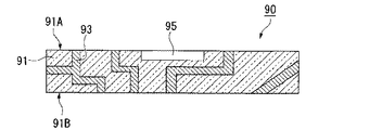
また図9は、基材91の一面91Aに機能素子95を埋設してなる点のみ図7の基材71と異なっている。図9に示すように、基材91はその内部に貫通配線93とは直接には電気的に接続されないように、機能素子95を配する形態(以下、機能素子を内包する複合基板とも呼ぶ)としてもよい。このような形態に好適な機能素子(以下、単にデバイスとも呼ぶ)95としては、例えば、コンデンサや抵抗などの受動素子、あるいは各種センサなどのMEMSデバイスが挙げられる。
9 differs from the
図10は、図8と同様に、機能素子105を備えた基材101Bを一方の基板として用い、この基材に設けた貫通配線の一端及び/又は他端が、接合する他の基板(基材101A)の電極に対応する位置に配されている構成である。図10(a)は他方の基板、図10(b)は一方の基板であり、図10(c)は2つの基材101A、101Bを接合した状態を示している。この構成によれば、両者の基板に設けた端部同士の位置がそれぞれ一致し、電気的な導通が可能になるとともに、機能素子105が2つの基材101A、101B間に挟み込まれ、あるいは密閉された形態とすることができるので、外力に対して耐久性に優れた構成が得られる。また、機能素子105が外部環境に曝される虞がないので、耐環境性の改善も図れる。
In FIG. 10, similarly to FIG. 8, the
本発明に係る貫通配線基板は、上述したように、基板内部で三次元的に自由な配線を可能とする貫通電極を基本構造としている。以下ではまず、上述した各種構成からなる貫通配線基板の製造方法について、図11〜図14に基づき、貫通配線基板が単板からなる場合を例として詳細に述べる。次いで、いくつかの具体的な態様を実施例1〜3として説明する。 As described above, the through wiring substrate according to the present invention has a basic structure of a through electrode that enables three-dimensional free wiring inside the substrate. Below, the manufacturing method of the penetration wiring board which consists of various structures mentioned above is described in detail based on the case where a penetration wiring board consists of a single board based on FIGS. 11-14. Next, some specific modes will be described as Examples 1 to 3.
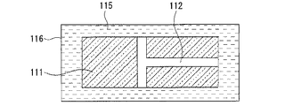
図11〜図14は、本発明に係る貫通配線基板の作製方法を工程順に示した模式的な断面図である。本実施形態では、基材として厚さが500μmのガラス(石英)基板を用いた。また本実施形態における微細孔の作製方法は、レーザーを用いて石英基板の一部を改質した後、改質した部分をエッチングにより除去するものである。 11 to 14 are schematic cross-sectional views showing a method of manufacturing a through wiring board according to the present invention in the order of steps. In the present embodiment, a glass (quartz) substrate having a thickness of 500 μm is used as the base material. In addition, the method for producing a microscopic hole in the present embodiment is to modify a part of a quartz substrate using a laser and then remove the modified part by etching.
まず、図11に示すように、石英からなる基板111の少なくとも微細孔を形成したい箇所にレーザー光118を照射して基板111内に改質部114を形成する。本実施形態においてはレーザー光118の光源としてフェムト秒レーザーを用い、基板111内部に焦点113を結ぶようにレーザービームを照射し、例えば径が数μm〜数十μmとした改質部114を得る。その際、焦点113と基板位置とを制御することにより、図12に例示するように様々な形状の改質部114を形成することができる。なお、微細孔を形成する基板111は、石英基板に限定されるものではなく、例えばサファイア等の絶縁基板や、アルカリ成分等を含んだ他の他成分ガラス基板を用いることができ、その厚さも150μm〜1mm程度まで適宜設定できる。
First, as shown in FIG. 11, a
次いで、図13に示すように、容器116内に入れた所定の薬液115中に、改質部を形成した基板111を浸漬する。これにより、改質部は薬液115によりウェットエッチングされ、基板111内から除去される。その結果、改質部が存在した部分に、微細孔112が形成される。本実施形態では、薬液115としてフッ酸を主成分とする酸溶液を用いた。
本エッチングは、改質部114が改質されていない部分に比べて非常に早くエッチングされる現象を利用するものであり、結果として改質部114に起因した形状の微細孔112を形成することができる。本実施形態においては、微細孔112の孔径は50μmとした。なお、薬液115はフッ酸に限定されず、例えばフッ酸に硝酸等を適量添加したフッ硝酸系の混酸等を用いることができる。また、微細孔112の孔径も、貫通電極の用途に応じて10μm程度から300μm程度まで適宜設定することができる。さらに、形成する微細孔も、基板を貫通するもの、非貫通のもののどちらでも良い。
Next, as shown in FIG. 13, the
This etching utilizes the phenomenon that the modified
上述した方法により、石英からなる基板の内部に三次元的に自由な構造を持つ微細孔を形成することができる。以下、いくつかの貫通電極の態様に応じた作製方法を説明する。 By the above-described method, a fine hole having a three-dimensional free structure can be formed inside a quartz substrate. Hereinafter, a manufacturing method according to some embodiments of the through electrode will be described.
(実施例1)・・・単板での実施
本例では、一枚の基板に貫通配線を配してなる貫通配線基板の作製方法について、図14に基づき詳述する。
まず、図14(a)に示すように、石英からなる基板141に前述した微細孔の形成方法により様々な形態をもつ微細孔142を形成する。ここで、基板141は厚さが500μmであり、微細孔142の孔径は50μmとした。なお、基板の厚さは孔径がこれに限定されないことは上述の通りである。
次いで、図14(b)に示すように、微細孔142の内部に導電性物質143を充填する。本例では、導電性物質143として金錫(Au−Sn)を用い、溶融金属充填法により微細孔内部に充填した。溶融金属充填法は、圧力差を用いて微細孔内部にも気密性よく短時間で充填できる方法である。なお、本例においては、充填金属として金錫(Au−Sn)を用いたが、本発明はこれに限定されず、異なる組成を有する金錫合金や、錫(Sn)、インジウム(In)等の金属、また錫鉛(Sn−Pb)系、錫(Sn)基、鉛(Pb)基。金(Au)基、インジウム(In)基、アルミニウム(Al)基等のはんだを使用することができる。また、充填方法も溶融金属吸引法を用いたが、本発明はこれに限定されず、めっき法による金属充填や印刷法による導電性ペーストの充填、またCVD等によるカーボンナノチューブの充填を利用することができる。
以上の方法により、三次元的に自由な貫通電極を有する貫通配線基板を提供することができる。
なお、本例においては、微細孔142は基板の主面あるいは側面を貫通するものであったが、本発明はこれに限定されず、微細孔は非貫通で形成しておき、金属充填後、基板を研磨することにより貫通電極を形成することも可能である。
(Embodiment 1)... Implementation with a single plate In this example, a method for manufacturing a through wiring substrate in which through wiring is arranged on a single substrate will be described in detail with reference to FIG.
First, as shown in FIG. 14A,
Next, as shown in FIG. 14B, the
By the above method, a through wiring substrate having a three-dimensional free through electrode can be provided.
In this example, the
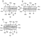
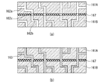
(実施例2)・・・複合基板の実施例
本例では、複数の貫通配線基板を積み重ねてなる複合基板の作製方法について、図15に基づき詳述する。ここでは、三通りの製法について例示する。
第一の製法(図15)は、実施例1において説明した方法により作製した貫通配線基板同士を積み重ねるものである。まず、図15(a)に示すように、既に貫通電極153(153a、153b)が形成された貫通配線基板151Aと151Bを対向させ、貫通電極153a、153bの端部同士の位置を合わせるようにアライメントを行う。その後、図15(b)に示すように、2つの貫通配線基板151A、151Bを積み重ねた。本例では、異方性導電接着剤157を用いて基板間を接着したが、これに限定されるものではなく、例えばはんだバンプを用いた接合など他の方法を用いてもよい。
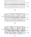
第二の製法(図16)は、まず、図16(a)に示すように、微細孔162a、162bのみが形成された基板161A、161Bを、絶縁樹脂163を介して接合する。この際、微細孔162aと162bが重なる位置にある樹脂は、予め(貼り合わせ前に)除去しておいても良いし、貼り合わせ後にエッチング等により除去しても良い。次いで、図16(b)に示すように、接合後に形成された微細孔162a、162b、162cに一度に金属充填し、貫通電極を作製するものである。本例では、絶縁樹脂163を用いて両基板を接着したが、これに限定されるものではなく、例えば陽極接合など他の方法を用いてもよい。
第三の製法(図17)は、まず、図17(a)に示すように、基板171Aと171Bを用意し、低融点ガラス177を用いて接合した状態とする。次いで、接合後の基板に微細孔172を形成する。その後、微細孔172の内部に金属充填するものである。本例では、低融点ガラス177を用いて両基板を接着したが、これに限定されるものではなく、例えば陽極接合など他の方法を用いてもよい。
以上の方法により、三次元的に自由な貫通電極を有する貫通配線基板を積層することができる。
Example 2 Example of Composite Substrate In this example, a method for manufacturing a composite substrate in which a plurality of through wiring substrates are stacked will be described in detail with reference to FIG. Here, three types of manufacturing methods are illustrated.
The first manufacturing method (FIG. 15) is a method of stacking through wiring substrates produced by the method described in the first embodiment. First, as shown in FIG. 15A, the through
In the second manufacturing method (FIG. 16), first, as shown in FIG. 16A,
In the third manufacturing method (FIG. 17), first, as shown in FIG. 17A,
By the above method, a through wiring substrate having a three-dimensional free through electrode can be laminated.
(実施例3)・・・パッケージへの応用例
実施例1、及び実施例2において説明した貫通電極及びそれを用いた貫通配線基板を適宜使用することにより、図18に示すように複数のデバイス(電子部品)185A〜185Dを三次元的に複合実装した機能キューブ(電子装置)を実現することができる。
なお、図18において、181A〜181Dは基板であり、特に複合実装した際、181Aは2つのデバイス185A、185Bを外面に、181Bはデバイス185Dを内面に、181Cはデバイス185Cを内面に、それぞれ載置している。
(Example 3) ... Application example to package By appropriately using the through electrode described in Example 1 and Example 2 and the through wiring substrate using the through electrode, a plurality of devices as shown in FIG. (Electronic component) A functional cube (electronic device) in which 185A to 185D are three-dimensionally combined and mounted can be realized.
In FIG. 18,
本発明によれば、基板内部を三次元的に自由に配線し、基板の表裏のみならず側面にも電気的な配線がなされるため、これまでの貫通配線と比べて、より設計の自由度が高く、高密度実装が可能となる。
また、本発明の貫通配線基板を提供することにより、三次元実装やSiPにおいて、より高機能、高密度なパッケージを実現することができ、ひいてはデバイスの高速化、高機能化に貢献する。
According to the present invention, the interior of the substrate is freely wired three-dimensionally, and electrical wiring is made not only on the front and back sides of the substrate, but also on the side surfaces. And high-density mounting is possible.
In addition, by providing the through wiring board of the present invention, it is possible to realize a package with higher functionality and higher density in three-dimensional mounting and SiP, thereby contributing to higher speed and higher functionality of the device.
10、20、30、40、50、60、70 貫通配線基板、
11、21、31、41、51、61、71 基材、
12、22、32、42、52、62、72 微細孔、
13、23、33、43、53、63、73 貫通配線、
81A、81B 基材、83A、83B 貫通配線、
91 基材、93 貫通配線、95 機能素子、
101A、101B 基材、105 機能素子、
111 基板、112 微細孔、113 焦点、114 改質部、115 薬液、116 容器、118 レーザー光、
141 基板、142 微細孔、143 導電性物質、
151A、151B 貫通配線基板、153a、153b 貫通電極、157 異方性導電接着剤、
161A、161B 基板、162a、162b 微細孔、163 絶縁樹脂、
171A、171B 基板、172 微細孔、177 低融点ガラス、
181A〜181D 基板、185A〜185D デバイス(電子部品)。
10, 20, 30, 40, 50, 60, 70 Penetration wiring board,
11, 21, 31, 41, 51, 61, 71 base material,
12, 22, 32, 42, 52, 62, 72
13, 23, 33, 43, 53, 63, 73 Through wiring,
81A, 81B base material, 83A, 83B through wiring,
91 base material, 93 through wiring, 95 functional elements,
101A, 101B base material, 105 functional elements,
111 substrate, 112 fine hole, 113 focal point, 114 modifying part, 115 chemical solution, 116 container, 118 laser beam,
141 substrate, 142 micropores, 143 conductive material,
151A, 151B through wiring board, 153a, 153b through electrode, 157 anisotropic conductive adhesive,
161A, 161B substrate, 162a, 162b micropore, 163 insulating resin,
171A, 171B substrates, 172 micropores, 177 low melting glass,
181A to 181D substrate, 185A to 185D device (electronic component).
Claims (7)
前記貫通配線は、少なくとも一部に、前記基材の厚み方向とは異なる方向に延びる部分を有することを特徴とする貫通配線基板。 A through-wiring board provided with a through-hole formed by arranging a fine hole so as to connect at least two surfaces constituting a base material, and filling the fine hole with a conductive substance,
The penetration wiring board, wherein the penetration wiring has at least a portion extending in a direction different from a thickness direction of the base material.
An electronic device comprising an electronic component mounted on the through wiring substrate according to claim 1 or the composite substrate according to claim 6.
Priority Applications (1)
| Application Number | Priority Date | Filing Date | Title |
|---|---|---|---|
| JP2005126244A JP2006303360A (en) | 2005-04-25 | 2005-04-25 | Through-wire board, composite board, and electronic apparatus |
Applications Claiming Priority (1)
| Application Number | Priority Date | Filing Date | Title |
|---|---|---|---|
| JP2005126244A JP2006303360A (en) | 2005-04-25 | 2005-04-25 | Through-wire board, composite board, and electronic apparatus |
Related Child Applications (2)
| Application Number | Title | Priority Date | Filing Date |
|---|---|---|---|
| JP2010283801A Division JP5248590B2 (en) | 2010-12-20 | 2010-12-20 | Electronic equipment |
| JP2010283803A Division JP2011066449A (en) | 2010-12-20 | 2010-12-20 | Method for manufacturing passing wiring substrate, method for manufacturing complex substrate, and method for manufacturing electronic device using passing wiring substrate and complex substrate formed by those manufacturing methods |
Publications (2)
| Publication Number | Publication Date |
|---|---|
| JP2006303360A true JP2006303360A (en) | 2006-11-02 |
| JP2006303360A5 JP2006303360A5 (en) | 2010-06-24 |
Family
ID=37471262
Family Applications (1)
| Application Number | Title | Priority Date | Filing Date |
|---|---|---|---|
| JP2005126244A Pending JP2006303360A (en) | 2005-04-25 | 2005-04-25 | Through-wire board, composite board, and electronic apparatus |
Country Status (1)
| Country | Link |
|---|---|
| JP (1) | JP2006303360A (en) |
Cited By (33)
| Publication number | Priority date | Publication date | Assignee | Title |
|---|---|---|---|---|
| JP2008203336A (en) * | 2007-02-16 | 2008-09-04 | Fujikura Ltd | Opto-electric composite substrate, manufacturing method thereof and electronic equipment |
| JP2008288577A (en) * | 2007-04-18 | 2008-11-27 | Fujikura Ltd | Substrate treatment method, through-wire substrate and its manufacturing method, and electronic component |
| JP2009064840A (en) * | 2007-09-04 | 2009-03-26 | Sanyo Electric Co Ltd | Solar cell |
| JP2009088474A (en) * | 2007-09-28 | 2009-04-23 | Samsung Electro-Mechanics Co Ltd | Inter layer conduction method for printed circuit board |
| EP2058855A2 (en) | 2007-11-09 | 2009-05-13 | Fujikura, Ltd. | Method of manufacturing semiconductor package |
| JP2009176926A (en) * | 2008-01-24 | 2009-08-06 | Fujikura Ltd | Through wiring substrate and manufacturing method thereof |
| JP2009246271A (en) * | 2008-03-31 | 2009-10-22 | Tdk Corp | Method of wiring to electronic element built-in substrate, and method of manufacturing electronic element built-in substrate |
| JP2010021269A (en) * | 2008-07-09 | 2010-01-28 | Fujikura Ltd | Through wiring board and method of manufacturing the same |
| JP2010073713A (en) * | 2008-09-16 | 2010-04-02 | Ngk Spark Plug Co Ltd | Method of manufacturing ceramic component |
| WO2010119652A1 (en) | 2009-04-14 | 2010-10-21 | 株式会社フジクラ | Electronic device mounting structure and electronic device mounting method |
| WO2010125814A1 (en) | 2009-04-28 | 2010-11-04 | 株式会社フジクラ | Device mounting structure and device mounting method |
| WO2011004559A1 (en) | 2009-07-10 | 2011-01-13 | 株式会社フジクラ | Through-wiring board and method of manufacturing same |
| WO2011004556A1 (en) | 2009-07-06 | 2011-01-13 | 株式会社フジクラ | Through-wiring board and method of manufacturing same |
| WO2011048858A1 (en) * | 2009-10-23 | 2011-04-28 | 株式会社フジクラ | Device mounting structure and device mounting method |
| WO2011048862A1 (en) * | 2009-10-23 | 2011-04-28 | 株式会社フジクラ | Device-mounting structure and device-mounting method |
| WO2011078345A1 (en) * | 2009-12-25 | 2011-06-30 | 株式会社フジクラ | Through-wired substrate and manufacturing method therefor |
| WO2011126108A1 (en) | 2010-04-08 | 2011-10-13 | 株式会社フジクラ | Method of forming microstructures, laser irradiation device, and substrate |
| WO2011125752A1 (en) | 2010-04-08 | 2011-10-13 | 株式会社フジクラ | Method of forming microstructures, laser irradiation device, and substrate |
| JP2011242240A (en) * | 2010-05-18 | 2011-12-01 | Dainippon Printing Co Ltd | Microchip and manufacturing method therefor |
| JP2012004601A (en) * | 2011-10-03 | 2012-01-05 | Fujikura Ltd | Method for manufacturing semiconductor package |
| WO2012017857A1 (en) * | 2010-08-05 | 2012-02-09 | 株式会社フジクラ | Electronic circuit chip and method of manufacturing electronic circuit chip |
| WO2012108316A1 (en) * | 2011-02-08 | 2012-08-16 | 株式会社フジクラ | Method for manufacturing substrate having micropore, and substrate |
| CN102741010A (en) * | 2010-02-05 | 2012-10-17 | 株式会社藤仓 | Surface microstructure formation method and substrate having surface microstructure |
| WO2012161317A1 (en) * | 2011-05-25 | 2012-11-29 | 株式会社フジクラ | Method of manufacturing base substance disposed with fine hole, and base substance disposed with fine hole |
| JP2013048197A (en) * | 2011-07-26 | 2013-03-07 | Kyocer Slc Technologies Corp | Wiring board |
| WO2013065450A1 (en) | 2011-11-04 | 2013-05-10 | 株式会社フジクラ | Method of manufacturing substrate provided with micropores |
| JPWO2012067177A1 (en) * | 2010-11-17 | 2014-05-12 | 株式会社フジクラ | Wiring board and manufacturing method thereof |
| JPWO2012153839A1 (en) * | 2011-05-12 | 2014-07-31 | 株式会社フジクラ | Through wiring board, electronic device package, and electronic component |
| US20140254120A1 (en) * | 2009-10-23 | 2014-09-11 | Fujikura Ltd. | Device packaging structure and device packaging method |
| US9129843B1 (en) * | 2014-06-12 | 2015-09-08 | Globalfoundries Inc. | Integrated inductor |
| JP2017228826A (en) * | 2016-06-20 | 2017-12-28 | 株式会社フジクラ | Waveguide and manufacturing method of waveguide |
| JP2020199748A (en) * | 2019-06-13 | 2020-12-17 | セイコーエプソン株式会社 | Wiring board, manufacturing method of wiring board, inkjet head, mems device, and oscillator |
| WO2021149836A1 (en) * | 2020-01-21 | 2021-07-29 | 軍生 木本 | Semiconductor apparatus, and inspection device for same |
Citations (11)
| Publication number | Priority date | Publication date | Assignee | Title |
|---|---|---|---|---|
| JPS5994441A (en) * | 1982-11-19 | 1984-05-31 | Nippon Denso Co Ltd | Semiconductor device |
| JPH05259599A (en) * | 1992-03-13 | 1993-10-08 | Matsushita Electric Works Ltd | Printed wiring board |
| JP2000216514A (en) * | 1999-01-27 | 2000-08-04 | Matsushita Electric Ind Co Ltd | Wiring board and its manufacture |
| JP2001203457A (en) * | 2000-01-18 | 2001-07-27 | Ibiden Co Ltd | Interlayer connection structure for laminated wiring board |
| JP2002210730A (en) * | 2001-01-19 | 2002-07-30 | Tokyo Instruments Inc | Method for laser-aid working |
| JP2003020257A (en) * | 2001-07-04 | 2003-01-24 | Hitachi Ltd | Wiring board, semiconductor device and method for manufacturing these |
| JP2003197811A (en) * | 2001-12-27 | 2003-07-11 | Hitachi Ltd | Glass substrate, manufacturing method thereof, wiring base board and semiconductor module |
| JP2004160618A (en) * | 2002-11-15 | 2004-06-10 | Seiko Epson Corp | Micro machine and method for manufacturing the same |
| JP2004311720A (en) * | 2003-04-07 | 2004-11-04 | Fujikura Ltd | Multilayer wiring board, base material therefor and its manufacturing method |
| JP2004363212A (en) * | 2003-06-03 | 2004-12-24 | Hitachi Metals Ltd | Wiring board with through-hole conductor |
| JP2005019576A (en) * | 2003-06-25 | 2005-01-20 | Hitachi Metals Ltd | Wiring board having through hole conductor |
-
2005
- 2005-04-25 JP JP2005126244A patent/JP2006303360A/en active Pending
Patent Citations (11)
| Publication number | Priority date | Publication date | Assignee | Title |
|---|---|---|---|---|
| JPS5994441A (en) * | 1982-11-19 | 1984-05-31 | Nippon Denso Co Ltd | Semiconductor device |
| JPH05259599A (en) * | 1992-03-13 | 1993-10-08 | Matsushita Electric Works Ltd | Printed wiring board |
| JP2000216514A (en) * | 1999-01-27 | 2000-08-04 | Matsushita Electric Ind Co Ltd | Wiring board and its manufacture |
| JP2001203457A (en) * | 2000-01-18 | 2001-07-27 | Ibiden Co Ltd | Interlayer connection structure for laminated wiring board |
| JP2002210730A (en) * | 2001-01-19 | 2002-07-30 | Tokyo Instruments Inc | Method for laser-aid working |
| JP2003020257A (en) * | 2001-07-04 | 2003-01-24 | Hitachi Ltd | Wiring board, semiconductor device and method for manufacturing these |
| JP2003197811A (en) * | 2001-12-27 | 2003-07-11 | Hitachi Ltd | Glass substrate, manufacturing method thereof, wiring base board and semiconductor module |
| JP2004160618A (en) * | 2002-11-15 | 2004-06-10 | Seiko Epson Corp | Micro machine and method for manufacturing the same |
| JP2004311720A (en) * | 2003-04-07 | 2004-11-04 | Fujikura Ltd | Multilayer wiring board, base material therefor and its manufacturing method |
| JP2004363212A (en) * | 2003-06-03 | 2004-12-24 | Hitachi Metals Ltd | Wiring board with through-hole conductor |
| JP2005019576A (en) * | 2003-06-25 | 2005-01-20 | Hitachi Metals Ltd | Wiring board having through hole conductor |
Cited By (65)
| Publication number | Priority date | Publication date | Assignee | Title |
|---|---|---|---|---|
| JP2008203336A (en) * | 2007-02-16 | 2008-09-04 | Fujikura Ltd | Opto-electric composite substrate, manufacturing method thereof and electronic equipment |
| JP2008288577A (en) * | 2007-04-18 | 2008-11-27 | Fujikura Ltd | Substrate treatment method, through-wire substrate and its manufacturing method, and electronic component |
| JP2009064840A (en) * | 2007-09-04 | 2009-03-26 | Sanyo Electric Co Ltd | Solar cell |
| JP2009088474A (en) * | 2007-09-28 | 2009-04-23 | Samsung Electro-Mechanics Co Ltd | Inter layer conduction method for printed circuit board |
| EP2058855A2 (en) | 2007-11-09 | 2009-05-13 | Fujikura, Ltd. | Method of manufacturing semiconductor package |
| JP2009117771A (en) * | 2007-11-09 | 2009-05-28 | Fujikura Ltd | Method of manufacturing semiconductor package |
| US8048804B2 (en) | 2007-11-09 | 2011-11-01 | Fujikura Ltd. | Method of manufacturing semiconductor package |
| US7875553B2 (en) | 2007-11-09 | 2011-01-25 | Fujikura Ltd. | Method of manufacturing semiconductor package |
| JP2009176926A (en) * | 2008-01-24 | 2009-08-06 | Fujikura Ltd | Through wiring substrate and manufacturing method thereof |
| JP2009246271A (en) * | 2008-03-31 | 2009-10-22 | Tdk Corp | Method of wiring to electronic element built-in substrate, and method of manufacturing electronic element built-in substrate |
| JP2010021269A (en) * | 2008-07-09 | 2010-01-28 | Fujikura Ltd | Through wiring board and method of manufacturing the same |
| JP2010073713A (en) * | 2008-09-16 | 2010-04-02 | Ngk Spark Plug Co Ltd | Method of manufacturing ceramic component |
| WO2010119652A1 (en) | 2009-04-14 | 2010-10-21 | 株式会社フジクラ | Electronic device mounting structure and electronic device mounting method |
| WO2010125814A1 (en) | 2009-04-28 | 2010-11-04 | 株式会社フジクラ | Device mounting structure and device mounting method |
| CN102422414A (en) * | 2009-04-28 | 2012-04-18 | 株式会社藤仓 | Device mounting structure and device mounting method |
| JPWO2011004556A1 (en) * | 2009-07-06 | 2012-12-13 | 株式会社フジクラ | Penetration wiring board and manufacturing method thereof |
| JP2012164998A (en) * | 2009-07-06 | 2012-08-30 | Fujikura Ltd | Through wiring substrate |
| US8785791B2 (en) | 2009-07-06 | 2014-07-22 | Fujikura Ltd. | Through wiring substrate and manufacturing method thereof |
| WO2011004556A1 (en) | 2009-07-06 | 2011-01-13 | 株式会社フジクラ | Through-wiring board and method of manufacturing same |
| CN102474982A (en) * | 2009-07-06 | 2012-05-23 | 株式会社藤仓 | Through-wiring board and method of manufacturing same |
| JP2013034000A (en) * | 2009-07-10 | 2013-02-14 | Fujikura Ltd | Manufacturing method of through wiring board |
| JPWO2011004559A1 (en) * | 2009-07-10 | 2012-12-13 | 株式会社フジクラ | Through wiring board |
| US20120103677A1 (en) * | 2009-07-10 | 2012-05-03 | Fujikura Ltd. | Through wiring substrate and manufacturing method thereof |
| JP2012134540A (en) * | 2009-07-10 | 2012-07-12 | Fujikura Ltd | Through wiring substrate manufacturing method |
| JP2012099819A (en) * | 2009-07-10 | 2012-05-24 | Fujikura Ltd | Method of manufacturing through-wiring board |
| CN102474983A (en) * | 2009-07-10 | 2012-05-23 | 株式会社藤仓 | Through-wiring board and method of manufacturing same |
| WO2011004559A1 (en) | 2009-07-10 | 2011-01-13 | 株式会社フジクラ | Through-wiring board and method of manufacturing same |
| CN102577637A (en) * | 2009-10-23 | 2012-07-11 | 株式会社藤仓 | Device-mounting structure and device-mounting method |
| WO2011048862A1 (en) * | 2009-10-23 | 2011-04-28 | 株式会社フジクラ | Device-mounting structure and device-mounting method |
| US20140254120A1 (en) * | 2009-10-23 | 2014-09-11 | Fujikura Ltd. | Device packaging structure and device packaging method |
| JP5085787B2 (en) * | 2009-10-23 | 2012-11-28 | 株式会社フジクラ | Device mounting structure manufacturing method |
| WO2011048858A1 (en) * | 2009-10-23 | 2011-04-28 | 株式会社フジクラ | Device mounting structure and device mounting method |
| EP2493273A4 (en) * | 2009-10-23 | 2013-10-16 | Fujikura Ltd | Device-mounting structure and device-mounting method |
| CN102598879A (en) * | 2009-10-23 | 2012-07-18 | 株式会社藤仓 | Device mounting structure and device mounting method |
| JP5085788B2 (en) * | 2009-10-23 | 2012-11-28 | 株式会社フジクラ | Device mounting structure |
| US20120205148A1 (en) * | 2009-10-23 | 2012-08-16 | Fujikura Ltd. | Device packaging structure and device packaging method |
| EP2493273A1 (en) * | 2009-10-23 | 2012-08-29 | Fujikura, Ltd. | Device-mounting structure and device-mounting method |
| JP2012178611A (en) * | 2009-10-23 | 2012-09-13 | Fujikura Ltd | Method for manufacturing device mounting structure |
| WO2011078345A1 (en) * | 2009-12-25 | 2011-06-30 | 株式会社フジクラ | Through-wired substrate and manufacturing method therefor |
| JP2011134982A (en) * | 2009-12-25 | 2011-07-07 | Fujikura Ltd | Through wiring board and method of manufacturing the same |
| EP2763514A1 (en) | 2009-12-25 | 2014-08-06 | Fujikura Ltd. | Interposer substrate and method of manufacturing the same |
| CN102741010A (en) * | 2010-02-05 | 2012-10-17 | 株式会社藤仓 | Surface microstructure formation method and substrate having surface microstructure |
| WO2011126108A1 (en) | 2010-04-08 | 2011-10-13 | 株式会社フジクラ | Method of forming microstructures, laser irradiation device, and substrate |
| WO2011125752A1 (en) | 2010-04-08 | 2011-10-13 | 株式会社フジクラ | Method of forming microstructures, laser irradiation device, and substrate |
| CN102802864A (en) * | 2010-04-08 | 2012-11-28 | 株式会社藤仓 | Method of forming microstructures, laser irradiation device, and substrate |
| JP2011218398A (en) * | 2010-04-08 | 2011-11-04 | Fujikura Ltd | Method for forming microstructure, laser irradiation device, and substrate |
| JP2011242240A (en) * | 2010-05-18 | 2011-12-01 | Dainippon Printing Co Ltd | Microchip and manufacturing method therefor |
| CN103038839A (en) * | 2010-08-05 | 2013-04-10 | 株式会社藤仓 | Electronic circuit chip and method of manufacturing electronic circuit chip |
| JPWO2012017857A1 (en) * | 2010-08-05 | 2013-10-03 | 株式会社フジクラ | Electronic circuit chip and method for manufacturing electronic circuit chip |
| WO2012017857A1 (en) * | 2010-08-05 | 2012-02-09 | 株式会社フジクラ | Electronic circuit chip and method of manufacturing electronic circuit chip |
| JPWO2012067177A1 (en) * | 2010-11-17 | 2014-05-12 | 株式会社フジクラ | Wiring board and manufacturing method thereof |
| WO2012108316A1 (en) * | 2011-02-08 | 2012-08-16 | 株式会社フジクラ | Method for manufacturing substrate having micropore, and substrate |
| JPWO2012153839A1 (en) * | 2011-05-12 | 2014-07-31 | 株式会社フジクラ | Through wiring board, electronic device package, and electronic component |
| JP5873488B2 (en) * | 2011-05-25 | 2016-03-01 | 株式会社フジクラ | Manufacturing method of substrate having micropores, and substrate having micropores |
| JPWO2012161317A1 (en) * | 2011-05-25 | 2014-07-31 | 株式会社フジクラ | Manufacturing method of substrate having micropores, and substrate having micropores |
| WO2012161317A1 (en) * | 2011-05-25 | 2012-11-29 | 株式会社フジクラ | Method of manufacturing base substance disposed with fine hole, and base substance disposed with fine hole |
| JP2013048197A (en) * | 2011-07-26 | 2013-03-07 | Kyocer Slc Technologies Corp | Wiring board |
| JP2012004601A (en) * | 2011-10-03 | 2012-01-05 | Fujikura Ltd | Method for manufacturing semiconductor package |
| WO2013065450A1 (en) | 2011-11-04 | 2013-05-10 | 株式会社フジクラ | Method of manufacturing substrate provided with micropores |
| JPWO2013065450A1 (en) * | 2011-11-04 | 2015-04-02 | 株式会社フジクラ | Method for manufacturing a substrate with fine holes |
| US9129843B1 (en) * | 2014-06-12 | 2015-09-08 | Globalfoundries Inc. | Integrated inductor |
| JP2017228826A (en) * | 2016-06-20 | 2017-12-28 | 株式会社フジクラ | Waveguide and manufacturing method of waveguide |
| JP2020199748A (en) * | 2019-06-13 | 2020-12-17 | セイコーエプソン株式会社 | Wiring board, manufacturing method of wiring board, inkjet head, mems device, and oscillator |
| JP7302318B2 (en) | 2019-06-13 | 2023-07-04 | セイコーエプソン株式会社 | Wiring board, wiring board manufacturing method, inkjet head, MEMS device, and oscillator |
| WO2021149836A1 (en) * | 2020-01-21 | 2021-07-29 | 軍生 木本 | Semiconductor apparatus, and inspection device for same |
Similar Documents
| Publication | Publication Date | Title |
|---|---|---|
| JP2006303360A (en) | Through-wire board, composite board, and electronic apparatus | |
| JP5153574B2 (en) | Mounting structure | |
| JP2005345473A (en) | Gyro-sensor comprising a plurality of component units and fabricating method thereof | |
| JP5372579B2 (en) | Semiconductor device, manufacturing method thereof, and electronic device | |
| JP5610105B1 (en) | Electronic component built-in module | |
| JP2008078475A (en) | Electronic component device | |
| JP2008300507A (en) | Wiring substrate and manufacturing process of the same | |
| JP2010135671A (en) | Semiconductor equipment and method of manufacturing the same | |
| JP6153471B2 (en) | Microelectronic units, stacked assemblies, systems, and modules | |
| JP5032456B2 (en) | Semiconductor device, interposer, and manufacturing method thereof | |
| JP2016152262A (en) | Printed-wiring board | |
| JPWO2012153839A1 (en) | Through wiring board, electronic device package, and electronic component | |
| TW201236532A (en) | Method for Producing an Electrical Circuit and Electrical Circuit | |
| JP2011066449A (en) | Method for manufacturing passing wiring substrate, method for manufacturing complex substrate, and method for manufacturing electronic device using passing wiring substrate and complex substrate formed by those manufacturing methods | |
| JP4879536B2 (en) | COMPOSITE BOARD, MANUFACTURING METHOD THEREOF, AND ELECTRONIC DEVICE | |
| JP2005183924A (en) | Semiconductor chip mounting substrate, semiconductor chip mounting structure, and semiconductor chip mounting method | |
| JP2008311267A (en) | Circuit module manufacturing method and circuit module | |
| JP5248590B2 (en) | Electronic equipment | |
| JP2014155132A (en) | Circuit board, and method of manufacturing the same | |
| EP2453725A1 (en) | Through-wiring board and method of manufacturing same | |
| JP5186774B2 (en) | Charge detection type sensor and package container used therefor | |
| JP2007227596A (en) | Semiconductor module and its manufacturing method | |
| JPWO2016166809A1 (en) | Imaging module and imaging module manufacturing method | |
| JP2010153492A (en) | Semiconductor package and manufacturing method thereof | |
| JP5376490B2 (en) | Manufacturing method of electronic component package |
Legal Events
| Date | Code | Title | Description |
|---|---|---|---|
| A621 | Written request for application examination |
Free format text: JAPANESE INTERMEDIATE CODE: A621 Effective date: 20071126 |
|
| A521 | Written amendment |
Free format text: JAPANESE INTERMEDIATE CODE: A523 Effective date: 20100511 |
|
| A977 | Report on retrieval |
Free format text: JAPANESE INTERMEDIATE CODE: A971007 Effective date: 20100519 |
|
| A131 | Notification of reasons for refusal |
Free format text: JAPANESE INTERMEDIATE CODE: A131 Effective date: 20100525 |
|
| A521 | Written amendment |
Free format text: JAPANESE INTERMEDIATE CODE: A523 Effective date: 20100726 |
|
| A131 | Notification of reasons for refusal |
Free format text: JAPANESE INTERMEDIATE CODE: A131 Effective date: 20101019 |
|
| A02 | Decision of refusal |
Free format text: JAPANESE INTERMEDIATE CODE: A02 Effective date: 20110301 |