JP2006278661A - Optical semiconductor element and its manufacturing method, and optical semiconductor device - Google Patents
Optical semiconductor element and its manufacturing method, and optical semiconductor device Download PDFInfo
- Publication number
- JP2006278661A JP2006278661A JP2005094854A JP2005094854A JP2006278661A JP 2006278661 A JP2006278661 A JP 2006278661A JP 2005094854 A JP2005094854 A JP 2005094854A JP 2005094854 A JP2005094854 A JP 2005094854A JP 2006278661 A JP2006278661 A JP 2006278661A
- Authority
- JP
- Japan
- Prior art keywords
- layer
- ridge
- semiconductor substrate
- contact layer
- semiconductor
- Prior art date
- Legal status (The legal status is an assumption and is not a legal conclusion. Google has not performed a legal analysis and makes no representation as to the accuracy of the status listed.)
- Pending
Links
Images


Classifications
-
- H—ELECTRICITY
- H01—ELECTRIC ELEMENTS
- H01S—DEVICES USING THE PROCESS OF LIGHT AMPLIFICATION BY STIMULATED EMISSION OF RADIATION [LASER] TO AMPLIFY OR GENERATE LIGHT; DEVICES USING STIMULATED EMISSION OF ELECTROMAGNETIC RADIATION IN WAVE RANGES OTHER THAN OPTICAL
- H01S5/00—Semiconductor lasers
- H01S5/20—Structure or shape of the semiconductor body to guide the optical wave ; Confining structures perpendicular to the optical axis, e.g. index or gain guiding, stripe geometry, broad area lasers, gain tailoring, transverse or lateral reflectors, special cladding structures, MQW barrier reflection layers
- H01S5/22—Structure or shape of the semiconductor body to guide the optical wave ; Confining structures perpendicular to the optical axis, e.g. index or gain guiding, stripe geometry, broad area lasers, gain tailoring, transverse or lateral reflectors, special cladding structures, MQW barrier reflection layers having a ridge or stripe structure
-
- B—PERFORMING OPERATIONS; TRANSPORTING
- B82—NANOTECHNOLOGY
- B82Y—SPECIFIC USES OR APPLICATIONS OF NANOSTRUCTURES; MEASUREMENT OR ANALYSIS OF NANOSTRUCTURES; MANUFACTURE OR TREATMENT OF NANOSTRUCTURES
- B82Y20/00—Nanooptics, e.g. quantum optics or photonic crystals
-
- H—ELECTRICITY
- H01—ELECTRIC ELEMENTS
- H01S—DEVICES USING THE PROCESS OF LIGHT AMPLIFICATION BY STIMULATED EMISSION OF RADIATION [LASER] TO AMPLIFY OR GENERATE LIGHT; DEVICES USING STIMULATED EMISSION OF ELECTROMAGNETIC RADIATION IN WAVE RANGES OTHER THAN OPTICAL
- H01S5/00—Semiconductor lasers
- H01S5/04—Processes or apparatus for excitation, e.g. pumping, e.g. by electron beams
- H01S5/042—Electrical excitation ; Circuits therefor
- H01S5/0425—Electrodes, e.g. characterised by the structure
- H01S5/04254—Electrodes, e.g. characterised by the structure characterised by the shape
-
- H—ELECTRICITY
- H01—ELECTRIC ELEMENTS
- H01L—SEMICONDUCTOR DEVICES NOT COVERED BY CLASS H10
- H01L2224/00—Indexing scheme for arrangements for connecting or disconnecting semiconductor or solid-state bodies and methods related thereto as covered by H01L24/00
- H01L2224/01—Means for bonding being attached to, or being formed on, the surface to be connected, e.g. chip-to-package, die-attach, "first-level" interconnects; Manufacturing methods related thereto
- H01L2224/42—Wire connectors; Manufacturing methods related thereto
- H01L2224/47—Structure, shape, material or disposition of the wire connectors after the connecting process
- H01L2224/48—Structure, shape, material or disposition of the wire connectors after the connecting process of an individual wire connector
- H01L2224/4805—Shape
- H01L2224/4809—Loop shape
- H01L2224/48091—Arched
-
- H—ELECTRICITY
- H01—ELECTRIC ELEMENTS
- H01L—SEMICONDUCTOR DEVICES NOT COVERED BY CLASS H10
- H01L2224/00—Indexing scheme for arrangements for connecting or disconnecting semiconductor or solid-state bodies and methods related thereto as covered by H01L24/00
- H01L2224/01—Means for bonding being attached to, or being formed on, the surface to be connected, e.g. chip-to-package, die-attach, "first-level" interconnects; Manufacturing methods related thereto
- H01L2224/42—Wire connectors; Manufacturing methods related thereto
- H01L2224/47—Structure, shape, material or disposition of the wire connectors after the connecting process
- H01L2224/48—Structure, shape, material or disposition of the wire connectors after the connecting process of an individual wire connector
- H01L2224/484—Connecting portions
- H01L2224/48463—Connecting portions the connecting portion on the bonding area of the semiconductor or solid-state body being a ball bond
- H01L2224/48465—Connecting portions the connecting portion on the bonding area of the semiconductor or solid-state body being a ball bond the other connecting portion not on the bonding area being a wedge bond, i.e. ball-to-wedge, regular stitch
-
- H—ELECTRICITY
- H01—ELECTRIC ELEMENTS
- H01S—DEVICES USING THE PROCESS OF LIGHT AMPLIFICATION BY STIMULATED EMISSION OF RADIATION [LASER] TO AMPLIFY OR GENERATE LIGHT; DEVICES USING STIMULATED EMISSION OF ELECTROMAGNETIC RADIATION IN WAVE RANGES OTHER THAN OPTICAL
- H01S2301/00—Functional characteristics
- H01S2301/17—Semiconductor lasers comprising special layers
- H01S2301/176—Specific passivation layers on surfaces other than the emission facet
-
- H—ELECTRICITY
- H01—ELECTRIC ELEMENTS
- H01S—DEVICES USING THE PROCESS OF LIGHT AMPLIFICATION BY STIMULATED EMISSION OF RADIATION [LASER] TO AMPLIFY OR GENERATE LIGHT; DEVICES USING STIMULATED EMISSION OF ELECTROMAGNETIC RADIATION IN WAVE RANGES OTHER THAN OPTICAL
- H01S5/00—Semiconductor lasers
- H01S5/02—Structural details or components not essential to laser action
- H01S5/022—Mountings; Housings
- H01S5/02208—Mountings; Housings characterised by the shape of the housings
- H01S5/02212—Can-type, e.g. TO-CAN housings with emission along or parallel to symmetry axis
-
- H—ELECTRICITY
- H01—ELECTRIC ELEMENTS
- H01S—DEVICES USING THE PROCESS OF LIGHT AMPLIFICATION BY STIMULATED EMISSION OF RADIATION [LASER] TO AMPLIFY OR GENERATE LIGHT; DEVICES USING STIMULATED EMISSION OF ELECTROMAGNETIC RADIATION IN WAVE RANGES OTHER THAN OPTICAL
- H01S5/00—Semiconductor lasers
- H01S5/02—Structural details or components not essential to laser action
- H01S5/024—Arrangements for thermal management
- H01S5/02461—Structure or details of the laser chip to manipulate the heat flow, e.g. passive layers in the chip with a low heat conductivity
-
- H—ELECTRICITY
- H01—ELECTRIC ELEMENTS
- H01S—DEVICES USING THE PROCESS OF LIGHT AMPLIFICATION BY STIMULATED EMISSION OF RADIATION [LASER] TO AMPLIFY OR GENERATE LIGHT; DEVICES USING STIMULATED EMISSION OF ELECTROMAGNETIC RADIATION IN WAVE RANGES OTHER THAN OPTICAL
- H01S5/00—Semiconductor lasers
- H01S5/04—Processes or apparatus for excitation, e.g. pumping, e.g. by electron beams
- H01S5/042—Electrical excitation ; Circuits therefor
- H01S5/0425—Electrodes, e.g. characterised by the structure
- H01S5/04252—Electrodes, e.g. characterised by the structure characterised by the material
-
- H—ELECTRICITY
- H01—ELECTRIC ELEMENTS
- H01S—DEVICES USING THE PROCESS OF LIGHT AMPLIFICATION BY STIMULATED EMISSION OF RADIATION [LASER] TO AMPLIFY OR GENERATE LIGHT; DEVICES USING STIMULATED EMISSION OF ELECTROMAGNETIC RADIATION IN WAVE RANGES OTHER THAN OPTICAL
- H01S5/00—Semiconductor lasers
- H01S5/10—Construction or shape of the optical resonator, e.g. extended or external cavity, coupled cavities, bent-guide, varying width, thickness or composition of the active region
- H01S5/16—Window-type lasers, i.e. with a region of non-absorbing material between the active region and the reflecting surface
-
- H—ELECTRICITY
- H01—ELECTRIC ELEMENTS
- H01S—DEVICES USING THE PROCESS OF LIGHT AMPLIFICATION BY STIMULATED EMISSION OF RADIATION [LASER] TO AMPLIFY OR GENERATE LIGHT; DEVICES USING STIMULATED EMISSION OF ELECTROMAGNETIC RADIATION IN WAVE RANGES OTHER THAN OPTICAL
- H01S5/00—Semiconductor lasers
- H01S5/20—Structure or shape of the semiconductor body to guide the optical wave ; Confining structures perpendicular to the optical axis, e.g. index or gain guiding, stripe geometry, broad area lasers, gain tailoring, transverse or lateral reflectors, special cladding structures, MQW barrier reflection layers
- H01S5/2054—Methods of obtaining the confinement
- H01S5/2081—Methods of obtaining the confinement using special etching techniques
-
- H—ELECTRICITY
- H01—ELECTRIC ELEMENTS
- H01S—DEVICES USING THE PROCESS OF LIGHT AMPLIFICATION BY STIMULATED EMISSION OF RADIATION [LASER] TO AMPLIFY OR GENERATE LIGHT; DEVICES USING STIMULATED EMISSION OF ELECTROMAGNETIC RADIATION IN WAVE RANGES OTHER THAN OPTICAL
- H01S5/00—Semiconductor lasers
- H01S5/30—Structure or shape of the active region; Materials used for the active region
- H01S5/34—Structure or shape of the active region; Materials used for the active region comprising quantum well or superlattice structures, e.g. single quantum well [SQW] lasers, multiple quantum well [MQW] lasers or graded index separate confinement heterostructure [GRINSCH] lasers
- H01S5/343—Structure or shape of the active region; Materials used for the active region comprising quantum well or superlattice structures, e.g. single quantum well [SQW] lasers, multiple quantum well [MQW] lasers or graded index separate confinement heterostructure [GRINSCH] lasers in AIIIBV compounds, e.g. AlGaAs-laser, InP-based laser
- H01S5/34326—Structure or shape of the active region; Materials used for the active region comprising quantum well or superlattice structures, e.g. single quantum well [SQW] lasers, multiple quantum well [MQW] lasers or graded index separate confinement heterostructure [GRINSCH] lasers in AIIIBV compounds, e.g. AlGaAs-laser, InP-based laser with a well layer based on InGa(Al)P, e.g. red laser
Abstract
Description
本発明は光半導体素子及びその製造方法並びにその光半導体素子を組み込んだ光半導体装置に係わり、例えば、リッジ構造のレーザダイオード(LD)の製造技術に適用して有効な技術に関する。 The present invention relates to an optical semiconductor element, a manufacturing method thereof, and an optical semiconductor device incorporating the optical semiconductor element, and relates to a technique effective when applied to, for example, a manufacturing technique of a laser diode (LD) having a ridge structure.
光半導体素子としての半導体レーザ(LD)は、光通信システムの光源や情報処理機器の光源として多用されている。CD,DVD機器,レーザプリンタ,POS,バーコードリーダをはじめ、文書ファイルシステムなどの情報処理機器の光源として可視光半導体レーザが使用されている。半導体レーザ素子(光半導体素子)の構造の一つとして、いわゆるリッジ構造が知られている(例えば、特許文献1)。 A semiconductor laser (LD) as an optical semiconductor element is widely used as a light source of an optical communication system and a light source of information processing equipment. Visible light semiconductor lasers are used as light sources for information processing equipment such as document file systems such as CD, DVD equipment, laser printers, POS, and barcode readers. A so-called ridge structure is known as one of the structures of a semiconductor laser element (optical semiconductor element) (for example, Patent Document 1).
特許文献1に記載の半導体レーザ装置はリッジストライプ構造の窒化物系半導体レーザ装置である。この半導体レーザ装置は、n型GaN半導体基板上にn型GaNバッファ層、変調ドープ超格子n型クラッド層、n型GaN光導波層、多重量子井戸活性層、p型GaN光導波層、変調ドープ超格子p型クラッド層及びp−Ganコンタクト層を多層成長させた構造になっている。これら多層成長層は有機金属気相成長法(MOCVD)によって形成される。多層成長層の形成においては、n型GaN半導体基板にMOCVDでn型GaNバッファ層を成長させる。次いで、MOCVDでn型クラッド層、n型GaN光導波層、多重量子井戸活性層、p型GaN光導波層、p型クラッド層及びp−Ganコンタクト層まで順次成長する。
The semiconductor laser device described in
また、リッジストライプを形成するために変調ドープ超格子p型クラッド層の途中までドライエッチング法で除去し、除去面にはSiO2絶縁膜を形成する。その後、リッジの最上層であるp−Ganコンタクト層上のSiO2絶縁膜を部分的に除去し、その除去部分にPtからなるp側電極を形成し、さらに配線のためのTi/Pt/Auからなるp側電極パッドを形成する。 Further, in order to form a ridge stripe, the modulation doped superlattice p-type cladding layer is partially removed by dry etching, and a SiO 2 insulating film is formed on the removed surface. Thereafter, the SiO 2 insulating film on the p-Gan contact layer which is the uppermost layer of the ridge is partially removed, a p-side electrode made of Pt is formed on the removed portion, and Ti / Pt / Au for wiring is further formed. A p-side electrode pad made of is formed.
DVD等に使用される半導体レーザ素子(レーザダイオード)は、高出力、高寿命が要求されるとともに、低価格化の要求がある。 Semiconductor laser elements (laser diodes) used for DVDs and the like are required to have high output and long life and to be low in price.
リッジ構造の半導体レーザ素子の製造において、多層成長層の形成を複数回のMOCVD処理で行うため、半導体レーザ素子の製造コストが高くなってしまう。 In the production of a semiconductor laser device having a ridge structure, the multilayer growth layer is formed by a plurality of MOCVD processes, so that the production cost of the semiconductor laser device is increased.
また、特許文献1に記載の半導体レーザ装置では、リッジの最上層の半導体層と電極(p側電極)を電気的に接続するため、リッジ頭部(上面)を覆う絶縁膜に、ホトリソグラフィ技術及びエッチング技術によってコンタクトホールを形成する。リッジ幅は2μmと狭いため、コンタクトホールをリッジ頭部の中央に合わせるためには高精度のホトリソグラフィ技術(ホトレジストの露光・現像)及びエッチング技術が必要となり、歩留り向上及び生産性向上にとって好ましいことではない。
Further, in the semiconductor laser device described in
そこで、本発明者は、製造プロセスを簡素化するため、多層成長層の形成を1回のMOCVD処理で行う半導体レーザ素子の製造技術について検討した。 Therefore, in order to simplify the manufacturing process, the present inventor has studied a manufacturing technique of a semiconductor laser device in which a multilayer growth layer is formed by a single MOCVD process.
図11乃至図14は本発明に先立って検討した半導体レーザ素子及びその製造方法に係わる図である。図11は半導体レーザ素子の概要を示す一部の断面図、図12は図11に示す半導体レーザ素子の一部を示す拡大断面図である。図13は半導体レーザ素子の製造方法において、多層成長工程からAuめっき形成工程までを示す各工程における半導体基板の模式的断面図である。図14は半導体レーザ素子の製造方法において、GaAsコンタクト層上に形成されるバリアメタル層の被覆性を示す半導体基板の模式的断面図である。 11 to 14 are diagrams relating to a semiconductor laser device and a method for manufacturing the same, which were studied prior to the present invention. 11 is a partial cross-sectional view showing an outline of the semiconductor laser device, and FIG. 12 is an enlarged cross-sectional view showing a part of the semiconductor laser device shown in FIG. FIG. 13 is a schematic cross-sectional view of a semiconductor substrate in each process showing a multilayer growth process to an Au plating formation process in the method of manufacturing a semiconductor laser device. FIG. 14 is a schematic cross-sectional view of a semiconductor substrate showing the coverage of a barrier metal layer formed on a GaAs contact layer in the method of manufacturing a semiconductor laser device.
半導体レーザ素子70は、図11の概要図に示すように、半導体基板71の第1の面(図11では上面)上に化合物半導体からなる多層成長層を有している。この多層成長層は、半導体基板71の第1の面上に順次形成されるn型バッファ層72、n型クラッド層(第1クラッド層)73、活性層74、p型クラッド層(第1の第2クラッド層)75、p型エッチストップ層76、p型クラッド層(第2の第2クラッド層)77、p型コンタクト層78を有している。半導体基板71はGaAs基板、n型バッファ層72はGaAs層、n型クラッド層73はAlGaInP層、活性層74は障壁層がAlGaInP層で井戸層がGaInP層からなる多重量子井戸構造の半導体層、p型クラッド層75はAlGaInP層、エッチストップ層76はGaInP層、p型クラッド層77はGaAs層でそれぞれ形成されている。
As shown in the schematic diagram of FIG. 11, the
半導体基板71の多層成長層を形成する第1の面はGaAs結晶の結晶面(001)に対してθほど傾斜する結晶面となっている(図15参照)。前記θは10°であり、半導体基板71の第1の面は<001>方向となる。
The first surface of the
半導体基板71の第1の面側には、2本の分離溝79,80がコンタクト層78の上面からp型クラッド層(第2の第2クラッド層)77の下面に至るまで形成され、分離溝79,80の底はエッチストップ層76で形成される構造になっている。2本の分離溝79,80で挟まれる部分はストライプ状のリッジ(突条)81となる。このリッジ81の幅は2μm程度である。
On the first surface side of the
半導体基板の第1の面側において、リッジ81の分離溝79,80に臨む各側面82,83(図12参照)から分離溝79,80を含みかつ分離溝79,80を越えて半導体基板側縁に至る部分を覆う絶縁膜84が設けられている(図12参照)。また、半導体基板の第1の面側には金属からなるバリアメタル層85が形成されている。このバリアメタル層85はリッジ81及び分離溝79,80を覆っている。さらにバリアメタル層85に重なるようにAuからなるAuめっき膜98が形成されて第1の電極(p電極)86が形成されている。図示はしないが、半導体基板71の第1の面の反対面となる第2の面には第2電極(n電極)が設けられている。
On the first surface side of the semiconductor substrate, the semiconductor substrate side includes the
このような半導体レーザ素子70においては、第1の電極(p電極)86と第2の電極(n電極)に所定の電圧を印加することによって、リッジ81の延在方向に直交する半導体レーザ素子70の両端面からレーザ光を出射する。電流を流すことによって、リッジ81に対応するストライプ状の活性層部分が光導波路(共振器)となり、この光導波路の両端がレーザ光を出射する出射面を形成する。
In such a
図13(a)〜(f)及び図14(a)〜(e)は、半導体レーザ素子70の製造各工程での半導体基板等を示す図である。図13(a)〜(f)は、多層成長、リッジ用CVD形成、リッジ形成(ドライエッチ)、リッジ形成(ウエットエッチ)、絶縁膜形成、コンタクト用レジスト塗布における半導体基板等の模式図である。また、図14(a)〜(e)は、コンタクト用露光・現像、コンタクト形成(CVD膜,ドライエッチ)、バリアメタル形成、第1の電極形成、基板研摩・第2の電極形成における半導体基板等を示す模式図である。
FIGS. 13A to 13F and FIGS. 14A to 14E are views showing a semiconductor substrate and the like in each process of manufacturing the
図13(a)の多層成長では、n型GaAsからなる半導体基板71の第1の面上にMOCVD(有機金属気相成長法)によって、n型バッファ層72、n型クラッド層73、活性層74、p型クラッド層75、p型エッチストップ層76、p型クラッド層77、コンタクト層78を一度の処理でそれぞれ所定厚さに形成する。一例であるが、n型バッファ層72は厚さ0.5μm、n型クラッド層73は厚さ2.0μm、活性層74は厚さ0.04μm、p型クラッド層75は厚さ0.3μm、p型エッチストップ層76は厚さ5nm、p型クラッド層77は厚さ1.2μm、コンタクト層78は厚さ0.4μmである。
In the multilayer growth of FIG. 13A, an n-
つぎに、図13(b)のリッジ用CVD形成では、CVD法によってコンタクト層78の上面に厚さが、例えば400nmのSiO2膜を形成する。その後、SiO2膜を常用のホトリソグラフィ技術とエッチング技術によってパターニングし、前記リッジ81を形成するためのストライプ状(帯状)のリッジ形成用エッチングマスク90と、このリッジ形成用エッチングマスク90からそれぞれ所定の距離離れた位置にフィールド用エッチングマスク91を形成する。
Next, in the ridge CVD formation of FIG. 13B, a SiO 2 film having a thickness of, for example, 400 nm is formed on the upper surface of the
つぎに、図13(c)に示すように、リッジ形成用エッチングマスク90及びフィールド用エッチングマスク91をマスクとしてコンタクト層78及びp型クラッド層77をドライエッチングによってエッチングして、2本の分離溝79,80を形成する。分離溝79,80の底面はp型エッチストップ層76によって形成される。2本の分離溝79,80に挟まれた部分は帯状(ストライプ状)のリッジ81となる。例えば、リッジ81の幅cは、2μmである。また、分離溝79,80の幅dは10μmである。リッジ形成用エッチングマスク90の幅(c)も2μmである。
Next, as shown in FIG. 13C, the
ドライエッチングでは、分離溝79,80の底隅のエッチングが不十分であることから、図13(d)に示すように、ウエットエッチを行って断面が四角形となるリッジ81を形成する。
In dry etching, since the bottom corners of the
つぎに、リッジ形成用エッチングマスク90及びフィールド用エッチングマスク91を除去した後、図13(e)に示すように、リッジ81及び分離溝79,80等を覆うように絶縁膜84をCVD法によって形成する。絶縁膜84は、例えば、200nm厚さのSiO2膜からなっている。
Next, after removing the ridge
つぎに、図13(f)に示すように、リッジ81の上部を構成するコンタクト層78(リッジ部コンタクト層78a)と電極との接続をとるためのコンタクト孔を形成するために、コンタクト用レジスト94をリッジ81及び分離溝79,80等全体を覆うように塗布する。
Next, as shown in FIG. 13 (f), a contact resist is formed in order to form a contact hole for connecting the contact layer 78 (
つぎに、図14(a)に示すように、絶縁膜84上に常用のホトリソグラフィ技術及びエッチング技術によってリッジ81部が開口部に位置するような開口95を有するホトマスク96を形成する。そして、ホトマスク96をマスクとして露出し、かつ現像する。これにより、リッジ81上のコンタクト用レジスト94は除去されてリッジ部コンタクト層78a上の絶縁膜84が露出する。また、ホトマスク96の開口95の幅mを12μm程度とリッジ幅よりも広くすることによって、リッジ部コンタクト層78aの両側部分を覆う絶縁膜84部分まで露出する。なお、ホトマスク96は図14(a)において、分かりやすいように分離溝79,80部分では浮いた状態で示してあるが、実際はコンタクト用レジスト94に密着する構造になっている。
Next, as shown in FIG. 14A, a
つぎに、ホトマスク96を除去した後、コンタクト孔形成のためのステップとしてリッジ81上に露出する絶縁膜84をドライエッチによって除去する。これにより、長方形断面のリッジ部コンタクト層78aが露出する。
Next, after removing the
つぎに、図14(c)に示すように、リッジ81及び分離溝79,80等を覆うように蒸着によってバリアメタル層85を形成する。これは第1の電極(p電極)86がAuで形成されるため、このAuがリッジ部コンタクト層78aに拡散し、半導体レーザの特性が劣化するのを防止するためである。一例をあげるならば、この蒸着では、Ti,Pt,Auの順で順次蒸着される。リッジ部コンタクト層78aとAuとの接触を阻止するバリアとしてPt層及びTi層が作用する。また、Au層はこの上に次工程で金めっきを行うことからその下地金属として設ける。Ti層は0.05μm、Pt層は0.1μm、Au層は0.3μmである。
Next, as shown in FIG. 14C, a
つぎに、図14(d)に示すように、金めっきを行い、バリアメタル層85上にAuめっき層98を形成して第1の電極(p電極)を形成する。Auめっき層98は、例えば3.5μmの厚さに形成され、蒸着による0.3μm厚さのAu層と一体となる。
Next, as shown in FIG. 14D, gold plating is performed to form an
つぎに、図14(e)に示すように、半導体基板71の第2の面を所定厚さ研摩して半導体基板71の厚さを所定の厚さに形成する。その後、半導体基板71の第2の面に下地電極99を蒸着で形成した後、下地電極99上にめっきによってAuめっき層を形成して第2の電極(n電極)100を形成する。第2の電極100は、例えば3.5μmの厚さに形成される。
Next, as shown in FIG. 14E, the second surface of the
これにより、半導体レーザ素子70が製造される。実際の製造ではウエハと呼称される広い面積の半導体基板が使用され、図14(e)の断面構造のものを並列に複数形成する。その後、ウエハをリッジ81に沿う方向に一定間隔で分断して短冊体を形成する。さらに、この短冊体を一定間隔で劈開して複数の半導体基板71を製造することになる。
Thereby, the
図11乃至図14は好ましくない状態の図で説明している。即ち、図15は図11のリッジ81部分を模式的にした拡大図である。図13及び図14の方法で製造した半導体基板71は、図15に示すように、リッジ部コンタクト層78aの上面の角部分がバリアメタル層85によって被覆されず、バリアメタル層85から外に突出し、Auからなる第1の電極(p電極)86に接触してしまい、Auがリッジ部コンタクト層78aに拡散してしまうことが分かった。
FIG. 11 to FIG. 14 are illustrated with drawings in an unfavorable state. That is, FIG. 15 is an enlarged view schematically showing the
この不良発生について分析検討した結果以下のことを知見した。半導体レーザ素子70の製造におけるバリアメタル層85の製造において、蒸着装置のテーブル上に載置されるウエハは、遊星運動する状態で蒸着が行われる。蒸着源は一方向から供給されるが、ウエハは遊星運動により、公転しつつ自転することから、万弁なく均一に各部に蒸着が行われるはずである。
As a result of analyzing and examining the occurrence of this defect, the following was found. In the manufacture of the
半導体レーザ素子70の特性向上のため、多層成長層を形成するウエハの第1の面、即ち、半導体基板71の第1の面は、GaAs結晶の結晶面(001)に対してθ(10°)ほど傾斜する結晶面となっている。この結果、図15に示すように、リッジ部コンタクト層78aの両側の面も半導体基板71の第1の面に90°の角度となる基線101からθほど傾いた斜面となる。この結果、リッジ部コンタクト層78aの両側の角部の角度は一方(図では左側)では鈍角となり、他方(図では右側)は鋭角となる。このため、鋭角となる角部は庇状となり、バリアメタル層85が連続して続かなくなり、矢印Aで示すように途絶えて段切れ状態になり易いことが判明した。また、リッジ81の上側部に対面する絶縁膜84も外側に張り出す構造となることから、この部分でもバリアメタル層85の段切れは発生し易い。バリアメタル層85は、例えば、0.04μm厚さのTi層、0.04μm厚さのMo層、0.04μm厚さのTi層を順次重ねた層、あるいは0.05μm厚さのTi層と0.1μm厚さのPtを重ねた層で形成される。いずれにしてもバリアメタル層85は薄いため、段切れが発生しやすい。バリアメタル層85をこのように薄くするのは、結晶とバリアメタルの熱膨張差による劣化が懸念される理由による。
In order to improve the characteristics of the
本発明の目的は、特性劣化が起き難い信頼性が高い光半導体素子及びその製造方法並びにその光半導体素子を組み込んだ光半導体装置を提供することにある。 An object of the present invention is to provide a highly reliable optical semiconductor element in which characteristic deterioration is unlikely to occur, a manufacturing method thereof, and an optical semiconductor device incorporating the optical semiconductor element.
本発明の他の目的は、光導波路上に位置するリッジを有する光半導体素子において、半導体層からなるリッジ内に金が拡散しない構造の光半導体素子の製造技術を提供することにある。 Another object of the present invention is to provide a manufacturing technique of an optical semiconductor device having a structure in which gold is not diffused into a ridge made of a semiconductor layer in an optical semiconductor device having a ridge positioned on an optical waveguide.
本発明の他の目的は、製造工程の簡素化による製品コストの低減を図ることにある。 Another object of the present invention is to reduce product cost by simplifying the manufacturing process.
本発明の前記ならびにそのほかの目的と新規な特徴は、本明細書の記述および添付図面からあきらかになるであろう。 The above and other objects and novel features of the present invention will be apparent from the description of this specification and the accompanying drawings.
本願において開示される発明のうち代表的なものの概要を簡単に説明すれば、下記のとおりである。 The following is a brief description of an outline of typical inventions disclosed in the present application.
(1)光半導体素子は、
第1の面及びこの第1の面の反対面となる第2の面を有する第1導電型(n型)のGaAsからなる半導体基板と、
前記半導体基板の第1の面上に形成され、第1導電型の半導体層(AlGaInP)からなる第1クラッド層と、
前記第1クラッド層上に形成され、AlGaInP層を障壁層とし、GaInP層を井戸層とする多重量子井戸構造からなる活性層と、
前記活性層上に形成され、第2導電型(p型)の半導体層(AlGaInP)からなる第2クラッド層と、
前記第2クラッド層上に形成され、第2導電型の半導体層(GaAs)からなるコンタクト層と、
前記コンタクト層の上面から前記第2クラッド層の中層に亘って設けられ、前記コンタクト層及び前記第2クラッド層をそれぞれ分離する並列配置の2本の分離溝と、
前記2本の分離溝に挟まれるストライプ状のリッジと、
前記コンタクト層の前記分離溝に臨む側部には、前記分離溝に向かって徐々に側部の厚さが薄くなるように上面に斜面が設けられ、
前記半導体基板の前記第1の面側において、
前記リッジの前記分離溝に臨む各側面から前記分離溝を含みかつ前記分離溝を越えて前記半導体基板側縁に至る部分を覆う絶縁膜と、
前記リッジを構成する前記コンタクト層部分及び前記絶縁膜を覆う金属(上層Au、中層Pt,下層Ti)からなるバリアメタル層と、
前記バリアメタル層上に形成されるAuからなる第1の電極(p電極)と、
前記半導体基板の前記第2の面に形成される第2の電極(n電極)とを有し、
前記半導体基板の前記第1の面はGaAs結晶の結晶面(001)に対して傾斜する結晶面となり、
前記コンタクト層の上面側部の前記斜面はGaAs結晶の結晶面(111)であることを特徴とする。
(1) The optical semiconductor element is
A semiconductor substrate made of GaAs of the first conductivity type (n-type) having a first surface and a second surface opposite to the first surface;
A first cladding layer formed on a first surface of the semiconductor substrate and made of a first conductivity type semiconductor layer (AlGaInP);
An active layer formed on the first cladding layer and having a multiple quantum well structure in which an AlGaInP layer is a barrier layer and a GaInP layer is a well layer;
A second cladding layer formed on the active layer and made of a second conductivity type (p-type) semiconductor layer (AlGaInP);
A contact layer formed on the second cladding layer and made of a second conductivity type semiconductor layer (GaAs);
Two separation grooves provided in parallel from the upper surface of the contact layer to the middle layer of the second cladding layer, each separating the contact layer and the second cladding layer;
A striped ridge sandwiched between the two separation grooves;
The side surface of the contact layer facing the separation groove is provided with a slope on the upper surface so that the thickness of the side portion gradually decreases toward the separation groove,
On the first surface side of the semiconductor substrate,
An insulating film that covers the portion that includes the separation groove from each side of the ridge facing the separation groove and reaches the semiconductor substrate side edge beyond the separation groove;
A barrier metal layer made of metal (upper layer Au, middle layer Pt, lower layer Ti) covering the contact layer portion and the insulating film constituting the ridge;
A first electrode (p electrode) made of Au formed on the barrier metal layer;
A second electrode (n electrode) formed on the second surface of the semiconductor substrate;
The first surface of the semiconductor substrate is a crystal plane inclined with respect to a crystal plane (001) of a GaAs crystal,
The slope on the upper surface side of the contact layer is a crystal plane (111) of a GaAs crystal.
また、前記リッジを構成する前記コンタクト層部分を覆う前記バリアメタル層と、前記リッジ側面を覆う前記絶縁膜は連続して繋がり、前記リッジを構成する前記コンタクト層部分の表面は前記バリアメタル層及び前記絶縁膜から露出していないことを特徴とする。 Further, the barrier metal layer covering the contact layer portion constituting the ridge and the insulating film covering the side surface of the ridge are continuously connected, and the surface of the contact layer portion constituting the ridge is the barrier metal layer and It is not exposed from the insulating film.
また、前記半導体基板の前記第1の面上に第1導電型の半導体層(GaAs)からなるバッファ層が形成され、前記バッファ層上に前記第1クラッド層が形成されていることを特徴とする。 Further, a buffer layer made of a first conductivity type semiconductor layer (GaAs) is formed on the first surface of the semiconductor substrate, and the first cladding layer is formed on the buffer layer. To do.
また、前記第2クラッド層は前記活性層の上面に形成される第1の第2クラッド層と、前記コンタクト層の下面に形成される第2の第2クラッド層とからなり、前記第1の第2クラッド層と前記第2の第2クラッド層との間には、第2導電型の半導体層(GaInP)からなり前記第2の第2クラッド層のエッチング速度よりもエッチング速度が遅いエッチストップ層が形成され、前記分離溝の底面は前記エッチストップ層によって形成されていることを特徴とする。 The second clad layer includes a first second clad layer formed on the upper surface of the active layer and a second second clad layer formed on the lower surface of the contact layer. An etch stop made of a second conductivity type semiconductor layer (GaInP) between the second cladding layer and the second second cladding layer and having an etching rate lower than that of the second second cladding layer. A layer is formed, and a bottom surface of the separation groove is formed by the etch stop layer.
このような半導体レーザ素子は以下の製造方法によって製造される。 Such a semiconductor laser device is manufactured by the following manufacturing method.
半導体レーザ素子は、
(a)第1の面及びこの第1の面の反対面となる第2の面を有する第1導電型(n型)のGaAsからなる前記半導体基板を準備する工程、
(b)前記半導体基板の前記第1の面に、第1導電型のAlGaInPからなる第1クラッド層、AlGaInP層を障壁層としGaInP層を井戸層とする多重量子井戸構造の活性層、第2導電型(p型)のAlGaInPからなる前記第2クラッド層及び第2導電型のGaAsからなるコンタクト層を順次積層するように連続的にエピタキシャル成長させる工程、
(c)被膜形成と前記被膜の選択的エッチングによって、前記コンタクト層上に1本のストライプ状のリッジ形成用エッチングマスクと、このリッジ形成用エッチングマスクの両側に所定の距離離れて位置するフィールド用エッチングマスクとを形成する工程、
(d)前記両エッチングマスクをマスクとして前記コンタクト層をその上面から下面に至るまで、ウエットエッチングによる異方性エッチングを行い、前記リッジ形成用エッチングマスク及び前記フィールド用エッチングマスクの下にエッチング縁が斜面となるリッジ部コンタクト層及びフィールド部コンタクト層を形成する工程、
(e)前記両エッチングマスク、前記リッジ部コンタクト層及び前記フィールド部コンタクト層をマスクとして、前記第2のクラッド層の所定深さまでドライエッチングして分離溝を形成し、かつ2本の分離溝に囲まれる突状ストライプのリッジを形成する工程、
(f)前記両エッチングマスクを除去した後、ウエットエッチングを行って前記リッジの幅を所定寸法にする工程、
(g)前記半導体基板の前記第1の面側全体に絶縁膜を形成する工程、
(h)前記半導体基板の前記リッジ上面の前記絶縁膜を除去する工程、
(i)前記半導体基板の前記第1の面側全体に蒸着(上層Au、中層Pt、下層Ti)によって金属からなるバリアメタル層を形成する工程、
(j)前記半導体基板の前記第1の面側全体にめっきによってAu層を形成して第1の電極を形成する工程、
(k)前記半導体基板の前記第2の面に第2の電極を形成する工程とによって製造される。
The semiconductor laser element is
(A) preparing the semiconductor substrate made of GaAs of the first conductivity type (n-type) having a first surface and a second surface opposite to the first surface;
(B) a first clad layer made of AlGaInP of the first conductivity type on the first surface of the semiconductor substrate; an active layer having a multiple quantum well structure in which the AlGaInP layer is a barrier layer and the GaInP layer is a well layer; A step of continuously epitaxially growing the second clad layer made of conductive type (p-type) AlGaInP and the contact layer made of GaAs of the second conductive type sequentially,
(C) By forming a film and selectively etching the film, one stripe-shaped ridge-forming etching mask is formed on the contact layer, and for a field located at a predetermined distance on both sides of the ridge-forming etching mask. Forming an etching mask;
(D) Using the both etching masks as a mask, anisotropic etching is performed by wet etching from the upper surface to the lower surface of the contact layer, and an etching edge is formed under the ridge forming etching mask and the field etching mask. A step of forming a ridge contact layer and a field contact layer to be inclined,
(E) Using the both etching masks, the ridge contact layer and the field contact layer as a mask, dry etching is performed to a predetermined depth of the second cladding layer to form a separation groove, and two separation grooves are formed. Forming a ridge of protruding stripes surrounded,
(F) removing both the etching masks, and performing wet etching to make the width of the ridge a predetermined dimension;
(G) forming an insulating film on the entire first surface side of the semiconductor substrate;
(H) removing the insulating film on the top surface of the ridge of the semiconductor substrate;
(I) forming a barrier metal layer made of metal by vapor deposition (upper layer Au, middle layer Pt, lower layer Ti) on the entire first surface side of the semiconductor substrate;
(J) forming an Au layer by plating on the entire first surface side of the semiconductor substrate to form a first electrode;
(K) A second electrode is formed on the second surface of the semiconductor substrate.
また、前記工程(b)では、前記半導体基板と前記第1クラッド層間に半導体層(GaAs)からなるバッファ層を形成するとともに、前記前記活性層と前記コンタクト層との間に第2導電型からなる第1の第2クラッド層、第2導電型のGaInPからなるエッチストップ層、第2導電型からなる第2の第2クラッド層を順次重ねて形成し、
前記工程(e)及び工程(f)のエッチングでは、前記コンタクト層の表面から前記エッチストップ層が露出する深さまでエッチングすることを特徴とする。
In the step (b), a buffer layer made of a semiconductor layer (GaAs) is formed between the semiconductor substrate and the first cladding layer, and a second conductivity type is formed between the active layer and the contact layer. A first second clad layer, an etch stop layer made of second conductivity type GaInP, and a second second clad layer made of the second conductivity type, which are sequentially stacked,
In the etching in the step (e) and the step (f), the etching is performed from the surface of the contact layer to a depth at which the etch stop layer is exposed.
また、前記工程(a)では、前記半導体基板の前記第1の面が結晶面(001)に対して傾斜する結晶面となるGaAs基板を準備し、
前記工程(b)のエピタキシャル成長では前記コンタクト層をGaAs層で形成し、
前記工程(d)のウエットエッチングによる異方性エッチングでは、前記コンタクト層の上面側部の前記斜面がGaAs結晶の結晶面(111)になるように形成することを特徴とする。
In the step (a), a GaAs substrate is prepared in which the first surface of the semiconductor substrate is a crystal plane inclined with respect to the crystal plane (001),
In the epitaxial growth of the step (b), the contact layer is formed of a GaAs layer,
The anisotropic etching by wet etching in the step (d) is characterized in that the slope on the upper side portion of the contact layer is formed to be a crystal plane (111) of a GaAs crystal.
(2)光半導体装置は、
パッケージと、
前記パッケージの内外に亘って延在する複数のリードと、
前記パッケージ内に配置される導電性のサブマウントに取り付けられる光半導体素子(半導体レーザ素子)と、
前記光半導体素子の各電極と前記リードを電気的に接続する接続手段と、
前記光半導体素子の出射面から出射されるレーザ光を前記パッケージの外部に案内する光学系とを有し、
前記光半導体素子は、
第1の面及びこの第1の面の反対面となる第2の面を有する第1導電型(n型)のGaAsからなる半導体基板と、
前記半導体基板の第1の面上に形成され、第1導電型の半導体層(AlGaInP)からなる第1クラッド層と、
前記第1クラッド層上に形成され、AlGaInP層を障壁層とし、GaInP層を井戸層とする多重量子井戸構造からなる活性層と、
前記活性層上に形成され、第2導電型(p型)の半導体層(AlGaInP)からなる第2クラッド層と、
前記第2クラッド層上に形成され、第2導電型の半導体層(GaAs)からなるコンタクト層と、
前記コンタクト層の上面から前記第2クラッド層の中層に亘って設けられ、前記コンタクト層及び前記第2クラッド層をそれぞれ分離する並列配置の2本の分離溝と、
前記2本の分離溝に挟まれるストライプ状のリッジと、
前記コンタクト層の前記分離溝に臨む側部には、前記分離溝に向かって徐々に側部の厚さが薄くなるように上面に斜面が設けられ、
前記半導体基板の前記第1の面側において、
前記リッジの前記分離溝に臨む各側面から前記分離溝を含みかつ前記分離溝を越えて前記半導体基板側縁に至る部分を覆う絶縁膜と、
前記リッジを構成する前記コンタクト層部分及び前記絶縁膜を覆う金属(上層Au、中層Pt,下層Ti)からなるバリアメタル層と、
前記バリアメタル層上に形成されるAuからなる第1の電極(p電極)と、
前記半導体基板の前記第2の面に形成される第2の電極(n電極)とを有し、
前記半導体基板の前記第1の面はGaAs結晶の結晶面(001)に対して傾斜する結晶面となり、
前記コンタクト層の上面側部の前記斜面はGaAs結晶の結晶面(111)であり、
前記半導体レーザ素子は前記第1の電極がサブマウントに接合材で接続されている構成になっている。
(2) The optical semiconductor device
Package and
A plurality of leads extending in and out of the package;
An optical semiconductor element (semiconductor laser element) attached to a conductive submount disposed in the package;
Connection means for electrically connecting each electrode of the optical semiconductor element and the lead;
An optical system for guiding laser light emitted from the emission surface of the optical semiconductor element to the outside of the package;
The optical semiconductor element is:
A semiconductor substrate made of GaAs of the first conductivity type (n-type) having a first surface and a second surface opposite to the first surface;
A first cladding layer formed on a first surface of the semiconductor substrate and made of a first conductivity type semiconductor layer (AlGaInP);
An active layer formed on the first cladding layer and having a multiple quantum well structure in which an AlGaInP layer is a barrier layer and a GaInP layer is a well layer;
A second cladding layer formed on the active layer and made of a second conductivity type (p-type) semiconductor layer (AlGaInP);
A contact layer formed on the second cladding layer and made of a second conductivity type semiconductor layer (GaAs);
Two separation grooves provided in parallel from the upper surface of the contact layer to the middle layer of the second cladding layer, each separating the contact layer and the second cladding layer;
A striped ridge sandwiched between the two separation grooves;
The side surface of the contact layer facing the separation groove is provided with a slope on the upper surface so that the thickness of the side portion gradually decreases toward the separation groove,
On the first surface side of the semiconductor substrate,
An insulating film that covers the portion that includes the separation groove from each side of the ridge facing the separation groove and reaches the semiconductor substrate side edge beyond the separation groove;
A barrier metal layer made of metal (upper layer Au, middle layer Pt, lower layer Ti) covering the contact layer portion and the insulating film constituting the ridge;
A first electrode (p electrode) made of Au formed on the barrier metal layer;
A second electrode (n electrode) formed on the second surface of the semiconductor substrate;
The first surface of the semiconductor substrate is a crystal plane inclined with respect to a crystal plane (001) of a GaAs crystal,
The slope of the upper surface side of the contact layer is a crystal plane (111) of a GaAs crystal,
The semiconductor laser element has a configuration in which the first electrode is connected to a submount with a bonding material.
また、前記半導体基板と前記第1クラッド層との間には第1導電型の半導体層(GaAs)からなるバッファ層が設けられ、
前記活性層と前記コンタクト層との間には、第2導電型の半導体層からなる第1の第2クラッド層、第2導電型の半導体層(GaInP)からなるエッチストップ層、第2導電型の半導体層からなる第2の第2クラッド層が順次積層された構造となり、
前記分離溝は前記コンタクト層及び前記第2の第2クラッド層を分離し、分離溝の底面は前記エッチストップ層で形成されていることを特徴とする。
Further, a buffer layer made of a first conductivity type semiconductor layer (GaAs) is provided between the semiconductor substrate and the first cladding layer,
Between the active layer and the contact layer, a first second cladding layer made of a second conductivity type semiconductor layer, an etch stop layer made of a second conductivity type semiconductor layer (GaInP), and a second conductivity type The second clad layer made of the semiconductor layer is sequentially laminated,
The separation groove separates the contact layer and the second second cladding layer, and a bottom surface of the separation groove is formed by the etch stop layer.
また、前記パッケージは、第1の面及びこの第1の面の反対面となる第2の面を有する金属板からなるステムと、前記ステムの前記第1の面を覆うように固定される帽子型のキャップとからなり、
前記キャップの前記ステムの前記第1の面に対面する天井部分には穴が設けられるとともに、前記穴は透明なガラス板で塞がれて窓が形成されてなり、
前記ステムには、前記第1の面から前記第2の面を貫通しかつ絶縁体を介して前記ステムに固定される前記外部電極端子を構成する複数のリードが設けられ、
前記ステムには、前記第2の面に電気的に接続され、前記リードに沿って延在する前記外部電極端子を構成するリードが設けられ、
前記ステムの前記第1の面には金属からなるヒートシンクが固定され、
前記ヒートシンクの一側面には前記サブマウントが固定され、
前記サブマウントには前記接合材を介して前記半導体レーザ素子の前記第1の電極が固定され、
前記半導体レーザ素子の前記第2の電極は前記ステムに絶縁体を介して固定される前記リードに導電性のワイヤを介して接続され、
前記キャップは前記ステムの前記第1の面上に位置する前記リード、前記ヒートシンク、前記半導体レーザ素子及び前記ワイヤを覆い、
前記半導体レーザ素子の端面である出射面から出射されたレーザ光は前記窓を通って前記パッケージの外に出射されるように構成されている。
The package includes a stem made of a metal plate having a first surface and a second surface opposite to the first surface, and a cap fixed so as to cover the first surface of the stem. With a mold cap,
A hole is provided in a ceiling portion facing the first surface of the stem of the cap, and the hole is closed with a transparent glass plate to form a window,
The stem is provided with a plurality of leads that constitute the external electrode terminal that penetrates the second surface from the first surface and is fixed to the stem via an insulator,
The stem is provided with a lead that constitutes the external electrode terminal that is electrically connected to the second surface and extends along the lead.
A heat sink made of metal is fixed to the first surface of the stem,
The submount is fixed to one side of the heat sink,
The first electrode of the semiconductor laser element is fixed to the submount through the bonding material,
The second electrode of the semiconductor laser element is connected to the lead fixed to the stem via an insulator via a conductive wire,
The cap covers the lead, the heat sink, the semiconductor laser element and the wire located on the first surface of the stem;
Laser light emitted from an emission surface which is an end surface of the semiconductor laser element is configured to be emitted out of the package through the window.
本願において開示される発明のうち代表的なものによって得られる効果を簡単に説明すれば、下記のとおりである。 The effects obtained by the representative ones of the inventions disclosed in the present application will be briefly described as follows.
前記(1)の手段によれば、(a)リッジの両側面は絶縁膜によって覆われ、リッジの上部を形成するリッジ部コンタクト層はその両側面が傾斜した面となり、リッジ部コンタクト層の上面両側の角部はいずれも鈍角となることから、リッジ部コンタクト層の上面側はバリアメタル層によって確実に被覆される。 According to the means (1), (a) both side surfaces of the ridge are covered with an insulating film, and the ridge contact layer forming the upper portion of the ridge is a surface inclined on both sides, and the upper surface of the ridge contact layer Since both corners are obtuse, the upper surface side of the ridge contact layer is reliably covered with the barrier metal layer.
(b)リッジ形成において、コンタクト層をエッチングによってリッジ部コンタクト層とフィールド部コンタクト層を形成した後、リッジ部コンタクト層の両側をそれぞれ前記斜面となるように形成する。その後、リッジ部コンタクト層及びフィールド部コンタクト層をマスクとして、ドライエッチ及びウエットエッチの2回のエッチングによって分離溝を形成する。この結果、斜面となるリッジ部コンタクト層の両側先端部分は分離溝内に突出する構造となるが、この突出した先端の少なくとも下面は絶縁膜によって覆われている。また、リッジ部コンタクト層の下側のリッジ形成部分である第2の第2クラッド層(p型クラッド層)の側面を覆う前記絶縁膜は、リッジ部コンタクト層の両側の突出部分よりも分離溝側に突出する。この結果、リッジ部コンタクト層を被覆するバリアメタル層はリッジ部コンタクト層の両側から突出する前記絶縁膜に重なる。従って、上記(a)の効果を有するバリアメタル層と絶縁膜は連なり、リッジ部コンタクト層を包むように被覆することになる。このため、リッジ部コンタクト層がAuで形成された第1の電極(p電極)に接触することがなくなり、Auがリッジ部コンタクト層に拡散することは抑止できる。これにより、特性の優れた半導体レーザ素子を製造することができる。 (B) In the ridge formation, the contact layer is formed by etching to form the ridge contact layer and the field contact layer, and then both sides of the ridge contact layer are formed to be the inclined surfaces. Thereafter, using the ridge contact layer and the field contact layer as a mask, an isolation groove is formed by dry etching and wet etching twice. As a result, the tip portions on both sides of the ridge contact layer serving as the slope project into the separation groove, but at least the lower surface of the projecting tip is covered with an insulating film. The insulating film covering the side surface of the second second clad layer (p-type clad layer), which is the ridge forming portion below the ridge contact layer, is separated from the protruding portions on both sides of the ridge contact layer. Protrudes to the side. As a result, the barrier metal layer covering the ridge contact layer overlaps the insulating film protruding from both sides of the ridge contact layer. Therefore, the barrier metal layer having the effect (a) and the insulating film are connected to cover the ridge contact layer. Therefore, the ridge contact layer does not come into contact with the first electrode (p electrode) formed of Au, and Au can be prevented from diffusing into the ridge contact layer. Thereby, a semiconductor laser device having excellent characteristics can be manufactured.
(c)第1の電極(p電極)とリッジ部コンタクト層を電気的に接続するコンタクト孔の形成はコンタクト用レジストの露光及び現像を行った後、セルフアラインで行う絶縁膜のエッチングによって形成するため、リッジ上方に正確にコンタクト孔が形成できる。これはリッジのさらなる狭小化となっても正確にコンタクト孔を形成することができることになる。 (C) The contact hole for electrically connecting the first electrode (p electrode) and the ridge contact layer is formed by exposing and developing the contact resist and then etching the insulating film by self-alignment. Therefore, the contact hole can be accurately formed above the ridge. This makes it possible to accurately form contact holes even if the ridge is further narrowed.
(d)半導体基板上の多層成長層の形成を1回のMOCVD法で形成するため、工程が少なくなり、製品コストの低減が達成できる。 (D) Since the multilayer growth layer on the semiconductor substrate is formed by a single MOCVD method, the number of processes is reduced, and the product cost can be reduced.
前記(2)の手段によれば、上記(1)の構成の半導体レーザ素子をパッケージ内に組み込んだ光半導体装置であることから、半導体レーザ素子のリッジ内に金が拡散して特性を劣化させるおそれがないことから、光半導体装置の信頼性が高くなる。 According to the means (2), since the semiconductor laser device having the structure (1) is incorporated in a package, gold diffuses into the ridge of the semiconductor laser device and deteriorates its characteristics. Since there is no fear, the reliability of the optical semiconductor device is increased.
以下、図面を参照して本発明の実施例を詳細に説明する。なお、発明の実施例を説明するための全図において、同一機能を有するものは同一符号を付け、その繰り返しの説明は省略する。 Hereinafter, embodiments of the present invention will be described in detail with reference to the drawings. In all the drawings for explaining the embodiments of the invention, those having the same function are given the same reference numerals, and their repeated explanation is omitted.
図1乃至図10は本発明の実施例1である光半導体素子(半導体レーザ素子)に係わる図である。図1乃至図5は光半導体素子(半導体レーザ素子)の構造に係わる図、図6乃至図8は半導体レーザ素子の製造方法に係わる図である。また、図9は本実施例1の光半導体素子を組み込んだ光半導体装置(半導体レーザ装置)の一部を切り欠いた斜視図であり、図10は半導体レーザ装置を構成するヒートシンクにサブマウントを介して固定される半導体レーザ素子を示す斜視図である。
1 to 10 are diagrams related to an optical semiconductor element (semiconductor laser element) which is
本実施例1では、0.6μm帯の赤色半導体レーザ(半導体レーザ素子)の製造に本発明を適用した例について説明する。また、本実施例1では第1導電型としてn型(N型)、第2導電型としてp型(P型)の波長が650nm帯の半導体レーザ素子の例について説明する。 In Example 1, an example in which the present invention is applied to the manufacture of a 0.6 μm band red semiconductor laser (semiconductor laser element) will be described. In the first embodiment, an example of a semiconductor laser device having a wavelength of 650 nm band of n-type (N-type) as the first conductivity type and p-type (P-type) as the second conductivity type will be described.
図1は本実施例1の光半導体素子(半導体レーザ素子)を本発明の特徴が分かりやすいように模式的に示した図である。また、図2乃至図5は製造される半導体レーザ素子1に係わる図である。
FIG. 1 is a diagram schematically showing an optical semiconductor element (semiconductor laser element) of Example 1 so that the features of the present invention can be easily understood. 2 to 5 are diagrams relating to the
光半導体素子(半導体レーザ素子)1は、図1の概要図に示すように、半導体基板2の第1の面(図1では上面)上に化合物半導体からなる多層成長層を有している。この多層成長層は、半導体基板2の第1の面上に順次形成されるn型バッファ層3、n型クラッド層(第1クラッド層)4、活性層5、p型クラッド層(第1の第2クラッド層)6、p型エッチストップ層7、p型クラッド層(第2の第2クラッド層)8、p型コンタクト層9を有している。半導体基板2は厚さ100μm弱のGaAs基板からなっている。n型バッファ層3は厚さ0.5μmのGaAs層で形成され、n型クラッド層(第1クラッド層)4は厚さ2.0μmのAlGaInPで形成されている。活性層5は、障壁層が厚さ5nmのAlGaInP層からなり、井戸層が厚さ6nmのGaInP層からなり、井戸層が3層となる多重量子井戸構造となっている。p型クラッド層は下層となるp型クラッド層(第1の第2クラッド層)6と、上層となるp型クラッド層(第2の第2クラッド層)8により形成され、p型クラッド層6とp型クラッド層8との間にはp型エッチストップ層7が形成されている。p型クラッド層(第1の第2クラッド層)6は厚さ0.3μmのAlGaInP層からなり、p型エッチストップ層7は厚さ5nmのGaInP層からなり、p型クラッド層(第2の第2クラッド層)8は厚さ1.2μmからなるAlGaInP層からなっている。また、p型コンタクト層9は厚さ0.4μmのGaAs層で形成されている。
As shown in the schematic diagram of FIG. 1, the optical semiconductor element (semiconductor laser element) 1 has a multilayer growth layer made of a compound semiconductor on a first surface (upper surface in FIG. 1) of a
半導体基板2の、多層成長層を形成する第1の面は前述のように、GaAs結晶の結晶面(001)に対してθほど傾斜する結晶面となっている。前記θは10°であり、半導体基板2の第1の面は<001>方向となっている。
As described above, the first surface of the
半導体基板2の第1の面側には、2本の分離溝10,11がp型コンタクト層9の上面からp型クラッド層(第2の第2クラッド層)8の下面に至るまで形成され、分離溝10,11の底はエッチストップ層7で形成される構造になっている。2本の分離溝10,11で挟まれる部分はストライプ状のリッジ(突状)12となる。このリッジ12の幅は2μm程度である。リッジ12は断面が四角形となる帯状(ストライプ状)のp型クラッド層(第2の第2クラッド層)8で形成される部分と、この上に重なるp型コンタクト層9で形成される四角形のリッジ部コンタクト層9aとからなっている。また説明の便宜上分離溝10,11の外側に広がる部分をフィールドと呼称する。
On the first surface side of the
リッジ12は、2本の分離溝10,11をエッチングによって形成するが、本実施例1ではp型クラッド層(第2の第2クラッド層)8をエッチングして分離溝10,11を形成する際、2回のエッチングを行う。1回目のエッチングはリッジ部コンタクト層9aをマスクとするドライエッチングであり、分離溝10,11の大方の形状を形成する。ドライエッチングはエッチング底の隅部が良好にエッチングされず除去予定部分が残留することから、この残留部分のエッチングと分離溝10,11の断面形状を整えるために、2回目のエッチングをウエットエッチングで行う。
In the
p型クラッド層(第2の第2クラッド層)8はリッジ部コンタクト層9aをマスクとするエッチングで形成するため、p型クラッド層(第2の第2クラッド層)8で形成されるリッジ部分の幅はリッジ部コンタクト層9aの幅よりも狭くなり、側面はリッジ部コンタクト層9aの両側先端から内側に位置することになる。換言するならば、リッジ部コンタクト層9aの両側の先端は分離溝10,11側にp型クラッド層(第2の第2クラッド層)8で形成されるリッジ部分よりも突出することになる。
Since the p-type cladding layer (second second cladding layer) 8 is formed by etching using the
また、リッジ部コンタクト層9aは、p型コンタクト層9の上面に形成したエッチング用マスクをマスクとするウエットエッチングによって形成する。この際、異方性エッチングを行うため、リッジ部コンタクト層9aの両側の上面部分は斜面17a,17bとなる。この斜面17a,17bはGaAs結晶面(111)となる。図1の左側端の斜面17aは右上がりの斜面となり、右側端の斜面17bは右下がりの斜面となる。この結果、リッジ部コンタクト層9aの両斜面17a,17bと上面とのなす角度は90°よりも大きい鈍角となる。リッジ部コンタクト層9aの上面とのなす角度は図1における左側で130°程度であり、右側で110°程度である。
The
一方、半導体基板の第1の面側において、リッジ12の分離溝10,11に臨む各側面18,19から分離溝10,11を含みかつ分離溝10,11を越えて半導体基板側縁に至る部分を覆う絶縁膜20が設けられている。また、半導体基板の第1の面側には金属からなるバリアメタル層21が形成されている。このバリアメタル層21はリッジ12及び分離溝10,11を覆っている。
On the other hand, on the first surface side of the semiconductor substrate, the side surfaces 18 and 19 facing the
図1及び図4に示すように、リッジ部コンタクト層9aの上面側は、上面17cと、上面17cの左側に連続して連なる斜面17aと、上面17cの右側に連続して連なる斜面17bとからなり、上面17cと斜面17a,17bとのなす角度も鈍角となることから、リッジ部コンタクト層9aの上面側を覆うバリアメタル層21は、上面17cと斜面17a,17bとの連続部分である角部上で途切れることがない。
As shown in FIGS. 1 and 4, the upper surface side of the
また、後述する製造方法から分かるが、リッジ部コンタクト層9aの両側先端部分は、リッジ12を形成するp型クラッド層(第2の第2クラッド層)8の側面を覆う絶縁膜20上に載る構造となる。このリッジ部コンタクト層9aを支えるような構造となる絶縁膜20上にはリッジ部コンタクト層9aを覆うバリアメタル層21が密着し、バリアメタル層21と絶縁膜20は連続して繋がる。従って、バリアメタル層21と絶縁膜20は、リッジ部コンタクト層9aを含むリッジ12部分を包むように覆う構造となる。
As can be seen from the manufacturing method described later, both end portions of the
他方、バリアメタル層21に重なってAuめっき層24が形成されている。バリアメタル層21とAuめっき層24によって第1の電極(p電極)22が形成されている。また、図2に示すが、半導体基板2の第1の面の反対面となる第2の面には第2の電極(n電極)23が設けられている。
On the other hand, an
このような半導体レーザ素子1においては、第1の電極(p電極)22と第2の電極(n電極)23に所定の電圧を印加することによって、リッジ12の延在方向に直交する半導体レーザ素子1の両端面からレーザ光を出射する。電流を流すことによって、リッジ12に対面するストライプ状の活性層部分が光導波路(共振器)となり、この光導波路の両端がレーザ光を出射する出射面を形成する。
In such a
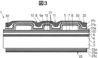
図2は実際に製造される半導体レーザ素子1を示す斜視図である。また、図3は図2のA−A線に沿う断面図を示すものである。そして、図4は図3のリッジ12部分をより明瞭に示す拡大断面図である。図5は、本実施例1の半導体レーザ素子1が、第1の面がGaAs結晶の結晶面(001)に対してθ(10°)傾斜する結晶面となる半導体基板を使用して製造するため、半導体基板を劈開して半導体レーザチップを製造した場合、半導体レーザ素子1の側面がθの角度傾斜することを強調して示す半導体レーザ素子1の端面図である。
FIG. 2 is a perspective view showing the
図2に示す半導体レーザ素子1では、点々を施して示す絶縁膜20は半導体基板2の第1の面側全域に設けられている。また、図2に示す半導体レーザ素子1では、ハッチングを施して示す上面の第1の電極(p電極)22は、バリアメタル層形成時の蒸着によって形成した金属を示す。この金属は、図2及び図3に示すように、例えば、最下層を形成する厚さ0.05μmのTi層21aと、Ti層21a上に形成される厚さ0.1μmのPt層21bと、Pt層21b上に形成される厚さ0.3μmのAu層21cとからなっている。リッジ部コンタクト層9aの上面17cと斜面17a,17bとのなす角度は、130°,110°と鈍角でその数値も大きいことから、リッジ部コンタクト層9aの上面側を覆うTi層21aは完全に覆う。図2及び図3ではTi層21a,Pt層21b,Au層21cを第1の電極(p電極)22と呼称している。
In the
図1に示す半導体レーザ素子1は、バリアメタル層形成のための蒸着処理後、Auめっきを行ったものであるところから、Au層21cとAuめっき層24は一体化することから、図1では第1の電極(p電極)22の最上層をAuめっき層24として表示してある。
Since the
また、図2に示すように、第1の電極(p電極)22は、共振器の両端部分上には一定長さ設けない構造とし、共振器端面部分に必要以上に電流を供給しない構造になっている。これは共振器端面での電流密度が高くなり、共振器端面が光学的に劣化するのを防止するためである。 In addition, as shown in FIG. 2, the first electrode (p electrode) 22 has a structure in which a certain length is not provided on both end portions of the resonator, and a structure in which current is not supplied more than necessary to the end face portion of the resonator. It has become. This is to prevent the current density at the resonator end face from increasing and the resonator end face from optically deteriorating.
図3に示すように、この半導体レーザ素子1では第2の電極(n電極)23は多層構造になっている。即ち、半導体基板2の第2の面には厚さ0.2μmのAuGeNi層23aと、このAuGeNi層23a上に重ねて形成される厚さ0.2μmのCr層23bと、このCr層23b上に重ねて形成される厚さ1.0μmのAu層23cとからなっている。
As shown in FIG. 3, in this
図4に示すように、Ti層21aが絶縁膜20と共にリッジ部コンタクト層9aを完全に覆っている。また、Pt層21bはリッジ12の上面全体を段切れを起こすことなく被覆する良好な状態の図となっている。これにより、Auとリッジ部コンタクト層9aは接触することがなく、Auがリッジ部コンタクト層9aに拡散されて半導体レーザ素子1の特性が劣化するようなこともない。
As shown in FIG. 4, the
図2及び図3に示す半導体レーザ素子1は、半導体基板2の第1の面側の側縁に分離溝10,11に沿う溝30を半導体基板2の一方の端(図2では右下端面)から他方の端(図2では左上端面)に亘って設ける構造であってもよい。この構造では、図3に示すように、溝30はp型エッチストップ層7が露出する深さ(第2クラッド層の中層)まで設けられている。そして、この溝30も絶縁膜20やバリアメタル層21に部分的に覆われている。この構造では、第1の電極(p電極)22の幅を半導体レーザ素子1の幅よりも狭くすることができる。
2 and 3 has a
本実施例1においては、n型バッファ層3を設けたが、n型バッファ層3を設けない構造にも適用できる。また、活性層5とp型コンタクト層9との間にp型クラッド層(第1の第2クラッド層)6,p型エッチストップ層7、p型クラッド層(第2の第2クラッド層)8を形成し、分離溝10,11をp型エッチストップ層7が溝底に現れるような構造としたが、活性層5とp型コンタクト層9との間にp型第2クラッド層を設け、分離溝10,11をp型第2クラッド層の中層部分まで設ける構造でも同様に適用することができる。
Although the n-
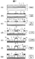
つぎに、図1に示す構造の半導体レーザ素子1の製造方法について図6乃至図8を参照しながら説明する。本実施例1の半導体レーザ素子1は、図6のフローチャートで示すように、多層成長(S01)、GaAsコンタクト層エッチング(S02)、リッジ形成(S03)、絶縁膜形成(S04)、コンタクト形成(S05)、バリアメタル層形成(S06)、第1の電極形成(S07)、基板第2の面研磨(S08)、第2の電極形成(S09)の各工程を経て製造される。
Next, a method for manufacturing the
図7(a)〜(g)は、多層成長、リッジ用CVD形成、GaAsコンタクト層エッチ、リッジ形成(ドライエッチ)、リッジ形成(ウエットエッチ)、絶縁膜形成、コンタクト用レジスト塗布の各工程における半導体基板等の模式図である。図8(a)〜(e)は、コンタクト用露光・現像、コンタクト形成(CVD膜,ドライエッチ)、バリアメタル形成、第1の電極形成、基板研摩・第2の電極形成の各工程における半導体基板等を示す模式図である。図7及び図8の各工程は図6のフローチャートで示す工程をさらに分かり易く細分化して示す工程図である。 FIGS. 7A to 7G show the steps of multilayer growth, CVD formation for ridge, GaAs contact layer etching, ridge formation (dry etching), ridge formation (wet etching), insulating film formation, and contact resist coating. It is a schematic diagram of a semiconductor substrate or the like. 8A to 8E show semiconductors in respective steps of contact exposure / development, contact formation (CVD film, dry etching), barrier metal formation, first electrode formation, substrate polishing / second electrode formation. It is a schematic diagram which shows a board | substrate etc. 7 and 8 are process diagrams showing the steps shown in the flowchart of FIG.
最初に、第1の面及びこの第1の面の反対面となる第2の面を有する第1導電型(n型)のGaAsからなる半導体基板2を準備する。この半導体基板2、多層成長層を形成する第1の面がGaAs結晶の結晶面(001)に対してθ(10°)ほど傾斜する結晶面となっている。半導体基板2の第1の面は<001>方向となる。
First, a
図7(a)の多層成長では、n型GaAsからなる半導体基板2の第1の面上にMOCVD(有機金属気相成長法)によって、n型バッファ層3、n型クラッド層(第1クラッド層)4、活性層5、p型クラッド層(第1の第2クラッド層)6、p型エッチストップ層7、p型クラッド層(第2の第2クラッド層)8、コンタクト層9を一度の処理でそれぞれ所定厚さに形成する。多層成長層を一回のMOCVD処理で形成することから、半導体レーザ素子1の製造コスキの低減が可能になる。一例であるが、n型バッファ層3は厚さ0.5μm、n型クラッド層73は厚さ2.0μm、活性層5は厚さ0.04μm、p型クラッド層(第1の第2クラッド層)6は厚さ0.3μm、p型エッチストップ層7は厚さ5nm、p型クラッド層(第2の第2クラッド層)8は厚さ1.2μm、p型コンタクト層9は厚さ0.4μmである。
7A, the n-
つぎに、図7(b)のリッジ用CVD形成では、CVD法によってコンタクト層9の上面に厚さが、例えば400nmのSiO2膜を形成する。その後、SiO2膜を常用のホトリソグラフィ技術とエッチング技術によってパターニングし、前記リッジ12を形成するためのストライプ状(帯状)のリッジ形成用エッチングマスク41と、このリッジ形成用エッチングマスク41からそれぞれ所定の距離離れた位置にフィールド用エッチングマスク42を形成する。
Next, in the ridge CVD formation of FIG. 7B, a SiO 2 film having a thickness of, for example, 400 nm is formed on the upper surface of the
つぎに、図7(c)のGaAsコンタクト層エッチでは、リッジ形成用エッチングマスク41及びフィールド用エッチングマスク42をマスクとしてコンタクト層9をウエットエッチングによる異方性エッチングによって分離溝10,11を形成する部分を除去する。このエッチングによって、リッジ形成用エッチングマスク41の下にはリッジ部コンタクト層9aが形成され、フィールド用エッチングマスク42の下にはフィールド部コンタクト層9bが形成される。
Next, in the GaAs contact layer etching of FIG. 7C, the
エッチング液はGaAs結晶に対して異方性エッチングを示す、POG(燐酸,過酸化水素水,エチレングリコールからなるエッチング液)を使用する。半導体基板2の第1面はGaAs結晶の結晶面(001)に対してθほど傾斜する結晶面となっている。このため、GaAs層からなるp型コンタクト層9も同じ結晶性を有する。異方性エッチングによってリッジ形成用エッチングマスク41の下面側に周り込んだエッチング液によってp型コンタクト層9の両側はそれぞれ斜面17a,17bとなる。この斜面17a,17bはGaAs結晶面(111)となる。図7(c)の左側端の斜面17aは右上がりの斜面となり、右側端の斜面17bは右下がりの斜面となる。この結果、リッジ部コンタクト層9aの両斜面17a,17bと上面とのなす角度は90°よりも大きい鈍角となる。リッジ部コンタクト層9aの上面とのなす角度は図1における左側で130°程度であり、右側で110°程度である。この斜面はフィールド用エッチングマスク42の下のフィールド部コンタクト層9bのエッチング端にも現れる。同図の矢印はエッチング方向を示す。
As the etching solution, POG (etching solution made of phosphoric acid, hydrogen peroxide solution, and ethylene glycol) that exhibits anisotropic etching with respect to the GaAs crystal is used. The first surface of the
つぎに、図7(d)のドライエッチングによるリッジ形成では、リッジ部コンタクト層9a及びフィールド部コンタクト層9bをマスクとしてp型クラッド層(第2の第2クラッド層)8をエッチングして分離溝10,11をさらに深くし、底面にp型エッチストップ層7が現れるようにする。この分離溝10,11はp型クラッド層(第2の第2クラッド層)8及びp型コンタクト層9を分断する。そして、この2本の分離溝10,11に挟まれた部分は帯状(ストライプ状)のリッジ12となる。例えば、リッジ12の幅aは、2μmである。また、分離溝10,11の幅dは10μmである。リッジ形成用エッチングマスク90の幅(c)は、例えば、2μmであり、dは10μmである。
Next, in the ridge formation by dry etching in FIG. 7D, the p-type cladding layer (second second cladding layer) 8 is etched using the
ドライエッチングでは、分離溝10,11の底隅のエッチングが不十分であることから、図7(e)に示すように、HF系あるいはHCl系のエッチング液を用いるウエットエッチによって断面が四角形となるリッジ12を形成する。この際、リッジ形成用エッチングマスク41及びフィールド用エッチングマスク42を除去した後、ウエットエッチングを行う。2回のエッチングにより、p型コンタクト層9のエッチング先端はリッジ12よりも突出(オーバーハング)するようになる。
In dry etching, the bottom corners of the
つぎに、図7(f)に示すように、リッジ12及び分離溝10,11等を覆うように絶縁膜20をCVD法によって形成する。絶縁膜20は、例えば、200nm厚さのSiO2膜からなっている。SiO2膜からなる絶縁保護膜は、垂直やオーバーハング部の構造部分を確実に被覆できる。
Next, as shown in FIG. 7F, an insulating
つぎに、図7(g)に示すように、リッジ12の上部を構成するリッジ部コンタクト層9aと電極との接続をとるためのコンタクト孔を形成するために、コンタクト用レジスト43をリッジ12及び分離溝10,11等全体を覆うように塗布する。
Next, as shown in FIG. 7G, in order to form a contact hole for connecting the
つぎに、図8(a)に示すように、絶縁膜20上に常用のホトリソグラフィ技術及びエッチング技術によってリッジ12部が開口部に位置するような開口44を有するホトマスク45を形成する。そして、ホトマスク45をマスクとして露出し、かつ現像する。これにより、リッジ12上のコンタクト用レジスト43は除去されてリッジ部コンタクト層9a上の絶縁膜20が露出する。また、ホトマスク45の開口44の幅mを12μm程度にすることによって、リッジ部コンタクト層9aの両側部分を覆う絶縁膜20部分まで露出する。なお、ホトマスク45は図8(a)において、分かりやすいように分離溝10,11部分では浮いた状態で示してあるが、実際はコンタクト用レジスト43に密着する構造になっている。
Next, as shown in FIG. 8A, a
つぎに、ホトマスク45を除去した後、コンタクト孔形成のためのステップとしてリッジ12上に露出する絶縁膜20をドライエッチによって除去する。これにより、リッジ部コンタクト層9aが露出する(図8(b)参照)。
Next, after the
つぎに、図8(c)に示すように、リッジ12及び分離溝10,11等を覆うように蒸着によってバリアメタル層21を形成する。これは第1の電極(p電極)22がAuで形成されるため、このAuがリッジ部コンタクト層9aに拡散し、半導体レーザの特性が劣化するのを防止するためである。一例をあげるならば、この蒸着では、Ti,Pt,Auの順で順次蒸着される。リッジ部コンタクト層9aとAuとの接触を阻止するバリアとしてPt層及びTi層が作用する。また、後工程で金めっきを行うことから最上層に薄くAuを設ける。Ti層は0.05μm、Pt層は0.1μm、Au層は0.3μmである。バリアとして用いる金属及びその組み合わせは実施例に限定されるものではない。
Next, as shown in FIG. 8C, a
バリアメタル形成において、リッジ12の両側面は絶縁膜20によって覆われ、リッジ12の上部を形成するリッジ部コンタクト層9aはその両側面が斜面17a,17bとなり、リッジ部コンタクト層9aの上面17cと斜面17a,17bとのなす角はいずれも鈍角となることから、リッジ部コンタクト層9aの上面側はバリアメタル層21によって確実に被覆される。
In the formation of the barrier metal, both side surfaces of the
また、リッジ形成において、p型コンタクト層9をエッチングによってリッジ部コンタクト層9aとフィールド部コンタクト層9bを形成した後、リッジ部コンタクト層9aの両側をそれぞれ前記斜面17a,17bとなるように形成する。その後、リッジ部コンタクト層9a及びフィールド部コンタクト層9bをマスクとして、ドライエッチ及びウエットエッチの2回のエッチングによって分離溝10,11を形成する。この結果、斜面17a,17bとなるリッジ部コンタクト層9aの両側先端部分は分離溝内に突出する構造となるが、この突出した先端の少なくとも下面は絶縁膜20によって覆われている。また、リッジ部コンタクト層9aの下側のリッジ形成部分であるp型クラッド層(第2の第2クラッド層)8の側面を覆う前記絶縁膜20は、リッジ部コンタクト層9aの両側の突出部分よりも分離溝側に突出する。この結果、リッジ部コンタクト層9aを被覆するバリアメタル層21はリッジ部コンタクト層9aの両側から突出する前記絶縁膜20に重なる。従って、リッジ部コンタクト層9aに対面するバリアメタル層21と絶縁膜20は連なり、リッジ部コンタクト層9aを包むように被覆することになる。このため、リッジ部コンタクト層9aがAuで形成される第1の電極(p電極)22と接触することがなくなり、Auがリッジ部コンタクト層9aに拡散することは抑止できる。
In the ridge formation, the p-
つぎに、図8(d)に示すように、金めっきを行い、バリアメタル層21上にAuめっき層を形成する。このAuめっき層は第1の電極(p電極)22を形成する。Auめっき層は半導体レーザ素子で発生する熱を効果的に放散するために厚く形成されている。Auめっき層は、例えば3.5μmの厚さに形成する。
Next, as shown in FIG. 8 (d), gold plating is performed to form an Au plating layer on the
つぎに、図8(e)に示すように、半導体基板2の第2の面を所定厚さ研摩して半導体基板2の厚さを所定の厚さに形成する。その後、半導体基板2の第2の面に下地電極47を蒸着で形成する。下地電極47は積層構造となり、例えば、AuGeNi層,Cr層,Au層と順次積層した構造になっている。その後、下地電極47上にめっきによってAuめっき層を形成して第2の電極(n電極)23を形成する。Auめっき層は、例えば3.5μmの厚さに形成される。図3ではAuめっき層は省略してある。
Next, as shown in FIG. 8E, the second surface of the
これにより、半導体レーザ素子1が製造される。実際の製造ではウエハと呼称される広い面積の半導体基板が使用され、図8(e)の断面構造のものを並列に複数形成する。その後、ウエハをリッジ12に沿う方向に一定間隔で分断して短冊体を形成する。さらに、この短冊体を一定間隔で劈開して複数の半導体基板2を製造することになる。
Thereby, the
このような半導体レーザ素子(光半導体素子)1は、パッケージ(封止容器)に組み込まれて半導体レーザ装置(光半導体装置)として使用される。図9は半導体レーザ素子1を組み込んだ光半導体装置(半導体レーザ装置)50の一例を示す。
Such a semiconductor laser device (optical semiconductor device) 1 is incorporated in a package (sealing container) and used as a semiconductor laser device (optical semiconductor device). FIG. 9 shows an example of an optical semiconductor device (semiconductor laser device) 50 incorporating the
半導体レーザ装置50は、第1の面及びこの第1の面の反対面となる第2の面を有する金属板(円板)からなる数mmの厚さのステム51と、このステム51の第1の面(図9では上面)を覆うように固定される帽子型のキャップ52とを有している。このステム51とキャップ52によってパッケージ53が形成される。
The
キャップ52の下部はフランジ部54を有し、このフランジ部54の下面が図示しない接合材によってステム51に接続されている。キャップ52の天井部分55には穴56が設けられるとともに、この穴56透明なガラス板57で塞がれて窓58が形成されている。この窓58からレーザ光がパッケージ53の外部に放射される。天井部分55はステム51の第1の面に対面している。
The lower portion of the
ステム51の第1の面の中央から外れた部分には銅製のヒートシンク59が導電性の鑞材等で固定されている。ヒートシンク59のステム51の中央に面する側面の先端側にはAlN(窒化アルミニウム)からなる熱伝導性が良好でかつ導電性のサブマウント60が固定されている(図10参照)。サブマウント60は半導体レーザ素子1よりも大きい矩形板からなっている。半導体レーザ素子1は細長く、その両端からレーザ光を出射するため、細長いサブマウント60はステム51に対して垂直な方向でヒートシンク59に固定される。この結果、半導体レーザ素子1の出射面は窓58に対面する構造になる。また、図示はしないが、サブマウント60の表面には、チップ固定部と、このチップ固定部から延在し先端部分が幅広のワイヤ接続パッドとを構成する導体層が設けられている。
A
一方、ステム51には3本のリード61a,61b,61cが固定されている。2本のリード61a,61bは絶縁体62を介してステム51に貫通状態で固定されている。残りの1本のリード61cはステム51の第1の面と反対面となる第2の面に突き合わせ状態で固定され、かつステム51と電気的に等電位状態になっている。
On the other hand, three
半導体レーザ素子1は符号は付さないが第1の電極(p電極)22がサブマウント60のチップ固定部に導電性の接合材を介して固定されている。従って、露出する半導体レーザ素子1の第2の面側は第2の電極(n電極)23が位置する。そこで、第2の電極(n電極)23と、ヒートシンク59を導電性のワイヤ63aで電気的に接続する。これにより、半導体レーザ素子1の第2の電極(n電極)23はリード61cに電気的に接続されることになる。また、サブマウント60の表面に設けられた前述の図示しないチップ固定部から延在した幅広のワイヤ接続パッドと、ステム51を貫通するリード61bのステム51の第1の面側に突出する先端とを導電性のワイヤ63bで電気的に接続する。これにより、半導体レーザ素子1の第1の電極(p電極)22はリード61cに電気的に接続されることになる。
Although the
以上のように、ステム51の第1の面側のヒートシンク59、リード61a,61b、サブマウント60、半導体レーザ素子1及びワイヤ63a,63bは、キャップ52によって覆われる構造になる。
As described above, the
半導体レーザ装置50において、リード61bとリード61c間に所定の電圧を印加すると半導体レーザ素子1の端面からレーザ光が出射され、このレーザ光は窓58を透過してステム51の外部に放射されることになる。
In the
半導体レーザ装置50は、上記半導体レーザ素子1をパッケージ53内に組み込んだ光半導体装置であることから、半導体レーザ素子1のリッジ内に金が拡散して特性を劣化させるおそれがなく、半導体レーザ装置(光半導体装置)の信頼性が高くなる。
Since the
本実施例では半導体レーザ素子1の出射面から出射されるレーザ光をパッケージ53の外部に案内する光学系は窓58としたが、光ファイバやレンズ等他の光学系でもよい。また、半導体レーザ素子1の電極とリードを電気的に接続する接続手段としてワイヤを使用したが、他の接続手段でもよい。
In this embodiment, the optical system for guiding the laser light emitted from the emission surface of the
本実施形態1によれば以下の効果を有する。 The first embodiment has the following effects.
(1)バリアメタル形成において、リッジ12の両側面は絶縁膜20によって覆われ、リッジ12の上部を形成するリッジ部コンタクト層9aはその両側面が斜面17a,17bとなり、リッジ部コンタクト層9aの上面17cと斜面17a,17bとのなす角はいずれも鈍角となることから、リッジ部コンタクト層9aの上面側はバリアメタル層21によって確実に被覆される。
(1) In barrier metal formation, both side surfaces of the
(2)リッジ形成において、p型コンタクト層9をエッチングによってリッジ部コンタクト層9aとフィールド部コンタクト層9bを形成した後、リッジ部コンタクト層9aの両側をそれぞれ前記斜面17a,17bとなるように形成する。その後、リッジ部コンタクト層9a及びフィールド部コンタクト層9bをマスクとして、ドライエッチ及びウエットエッチの2回のエッチングによって分離溝10,11を形成する。この結果、斜面17a,17bとなるリッジ部コンタクト層9aの両側先端部分は分離溝内に突出する構造となるが、この突出した先端の少なくとも下面は絶縁膜20によって覆われている。また、リッジ部コンタクト層9aの下側のリッジ形成部分であるp型クラッド層(第2の第2クラッド層)8の側面を覆う前記絶縁膜20は、リッジ部コンタクト層9aの両側の突出部分よりも分離溝側に突出する。この結果、リッジ部コンタクト層9aを被覆するバリアメタル層21はリッジ部コンタクト層9aの両側から突出する前記絶縁膜20に重なる。従って、リッジ部コンタクト層9aに対面するバリアメタル層21と絶縁膜20は連なり、リッジ部コンタクト層9aを包むように被覆することになる。このため、リッジ部コンタクト層9aがAuで形成される第1の電極(p電極)22と接触することがなくなり、Auがリッジ部コンタクト層9aに拡散することは抑止できる。これにより、特性の優れた半導体レーザ素子1を製造することができる。
(2) In the ridge formation, the p-
(3)第1の電極(p電極)22とリッジ部コンタクト層9aを電気的に接続するコンタクト孔の形成はコンタクト用レジスト43の露光及び現像を行った後、セルフアラインで行う絶縁膜20のエッチングによって形成するため、リッジ上方に正確にコンタクト孔が形成できる。これはリッジ12のさらなる狭小化となっても正確にコンタクト孔を形成することができることになる。
(3) The contact hole for electrically connecting the first electrode (p electrode) 22 and the
(4)半導体基板上の多層成長層の形成を1回のMOCVD法で形成するため、工程が少なくなり、製品コストの低減が達成できる。 (4) Since the multi-layer growth layer on the semiconductor substrate is formed by a single MOCVD method, the number of steps is reduced, and the product cost can be reduced.
(5)半導体レーザ装置50は、上記(1)及び(2)の効果を有する半導体レーザ素子1をパッケージ53内に組み込んだ光半導体装置であることから、半導体レーザ素子1のリッジ内に金が拡散して特性を劣化させるおそれがないことから、光半導体装置の信頼性が高くなる。
(5) Since the
以上本発明者によってなされた発明を実施形態に基づき具体的に説明したが、本発明は上記実施形態に限定されるものではなく、その要旨を逸脱しない範囲で種々変更可能であることはいうまでもない。実施例ではバリアメタル層としてPtを使用した例について説明したが、他の金属、例えば、Ni,Pd,Mo等による導体層をバリアメタル層としても前記実施例同様の効果を有することができる。 Although the invention made by the present inventor has been specifically described based on the embodiment, the present invention is not limited to the embodiment described above, and various modifications can be made without departing from the scope of the invention. Nor. In the embodiment, an example in which Pt is used as the barrier metal layer has been described. However, the same effect as in the above embodiment can be obtained by using a conductor layer of another metal, for example, Ni, Pd, Mo, or the like as the barrier metal layer.
また、実施例では0.6μm帯の半導体レーザ素子に本発明を適用した例について示したが、他の半導体レーザ素子、例えば、光通信用の長波長半導体レーザ素子(1.3μm帯,1.5μm帯)を組み込む光半導体装置にも同様に適用できる。 In the embodiments, an example in which the present invention is applied to a 0.6 μm band semiconductor laser element has been described. However, other semiconductor laser elements such as a long wavelength semiconductor laser element (1.3 μm band, 1.. The present invention can be similarly applied to an optical semiconductor device incorporating a 5 μm band).
1…光半導体素子(半導体レーザ素子)、2…半導体基板、3…n型バッファ層、4…n型クラッド層(第1クラッド層)、5…活性層、6…p型クラッド層(第1の第2クラッド層)、7…p型エッチストップ層、8…p型クラッド層(第2の第2クラッド層)、9…p型コンタクト層、9a…リッジ部コンタクト層、9b…フィールド部コンタクト層、10,11…分離溝、12…リッジ(突条)、17a,17b…斜面、17c…上面、18,19…側面、20…絶縁膜、21…バリアメタル層、21a…Ti層、21b…Pt層、21c…Au層、22…第1の電極(p電極)、23…第2の電極(n電極)、23a…AuGeNi層、23b…Cr層、23c…Au層、24…Auめっき層、30…溝、41…リッジ形成用エッチングマスク、42…フィールド用エッチングマスク、43…コンタクト用レジスト、44…開口、45…ホトマスク、47…下地電極、50…光半導体装置(半導体レーザ装置)、51…ステム、52…キャップ、53…パッケージ、54…フランジ部、55…天井部分、56…穴、57…ガラス板、58…窓、59…ヒートシンク、60…サブマウント、61a,61b,61c…リード、62…絶縁体、63,63a,63b…ワイヤ、70…半導体レーザ素子、73…n型クラッド層(第1クラッド層)、74…活性層、75…p型クラッド層(第1の第2クラッド層)、76…エッチストップ層、77…p型クラッド層(第2の第2クラッド層)、78…コンタクト層、78a…リッジ部コンタクト層、79,80…分離溝、81…リッジ(突条)、82,83…側面、84…絶縁膜、85…バリアメタル層、86…第1の電極(p電極)、90…リッジ形成用エッチングマスク、91…フィールド用エッチングマスク、94…コンタクト用レジスト、95…開口、96…ホトマスク、98…Auめっき層、99…下地電極、100…第2の電極、101…基線
DESCRIPTION OF
Claims (19)
前記半導体基板の第1の面上に形成され、第1導電型の半導体層からなる第1クラッド層と、
前記第1クラッド層上に形成される活性層と、
前記活性層上に形成され、第2導電型の半導体層からなる第2クラッド層と、
前記第2クラッド層上に形成され、第2導電型の半導体層からなるコンタクト層と、
前記コンタクト層の上面から前記第2クラッド層の中層に亘って設けられ、前記コンタクト層及び前記第2クラッド層をそれぞれ分離する並列配置の2本の分離溝と、
前記2本の分離溝に挟まれるストライプ状のリッジと、
前記コンタクト層の前記分離溝に臨む側部には、前記分離溝に向かって徐々に側部の厚さが薄くなるように上面に斜面が設けられ、
前記半導体基板の前記第1の面側において、
前記リッジの前記分離溝に臨む各側面から前記分離溝を含みかつ前記分離溝を越えて前記半導体基板側縁に至る部分を覆う絶縁膜と、
前記リッジを構成する前記コンタクト層部分及び前記絶縁膜を覆う金属からなるバリアメタル層と、
前記バリアメタル層上に形成される第1の電極と、
前記半導体基板の前記第2の面に形成される第2の電極とを有することを特徴とする光半導体素子。 A semiconductor substrate of the first conductivity type having a first surface and a second surface opposite to the first surface;
A first cladding layer formed on a first surface of the semiconductor substrate and made of a semiconductor layer of a first conductivity type;
An active layer formed on the first cladding layer;
A second cladding layer formed on the active layer and made of a semiconductor layer of a second conductivity type;
A contact layer formed on the second cladding layer and made of a second conductivity type semiconductor layer;
Two separation grooves provided in parallel from the upper surface of the contact layer to the middle layer of the second cladding layer, each separating the contact layer and the second cladding layer;
A striped ridge sandwiched between the two separation grooves;
The side surface of the contact layer facing the separation groove is provided with a slope on the upper surface so that the thickness of the side portion gradually decreases toward the separation groove,
On the first surface side of the semiconductor substrate,
An insulating film that covers the portion that includes the separation groove from each side of the ridge facing the separation groove and reaches the semiconductor substrate side edge beyond the separation groove;
A barrier metal layer made of metal covering the contact layer portion and the insulating film constituting the ridge;
A first electrode formed on the barrier metal layer;
An optical semiconductor device comprising: a second electrode formed on the second surface of the semiconductor substrate.
前記リッジを構成する前記コンタクト層部分の表面は前記バリアメタル層及び前記絶縁膜から露出していないことを特徴とする請求項1に記載の光半導体素子。 The barrier metal layer covering the contact layer portion constituting the ridge and the insulating film covering the side surface of the ridge are continuously connected,
2. The optical semiconductor element according to claim 1, wherein the surface of the contact layer portion constituting the ridge is not exposed from the barrier metal layer and the insulating film.
前記バッファ層上に前記第1クラッド層が形成されていることを特徴とする請求項1に記載の光半導体素子。 A buffer layer made of a semiconductor layer of a first conductivity type is formed on the first surface of the semiconductor substrate;
The optical semiconductor element according to claim 1, wherein the first cladding layer is formed on the buffer layer.
前記第1の第2クラッド層と前記第2の第2クラッド層との間には、第2導電型の半導体層からなり、前記第2の第2クラッド層のエッチング速度よりもエッチング速度が遅い材質からなるエッチストップ層が形成され、
前記分離溝の底面は前記エッチストップ層によって形成されていることを特徴とする請求項1に記載の光半導体素子。 The second cladding layer comprises a first second cladding layer formed on the upper surface of the active layer and a second second cladding layer formed on the lower surface of the contact layer,
Between the 1st 2nd clad layer and the 2nd 2nd clad layer, it consists of a semiconductor layer of the 2nd conductivity type, and an etching rate is slower than an etching rate of the 2nd 2nd clad layer An etch stop layer made of material is formed,
The optical semiconductor device according to claim 1, wherein a bottom surface of the separation groove is formed by the etch stop layer.
前記溝は前記第2クラッド層の中層まで設けられ、
前記リッジ側の溝側面及び前記溝底は前記バリアメタル層で覆われていることを特徴とする請求項1に記載の光半導体素子。 A groove along the separation groove is provided from one end of the semiconductor substrate to the other end at the side edge on the first surface side of the semiconductor substrate,
The groove is provided up to a middle layer of the second cladding layer;
The optical semiconductor element according to claim 1, wherein the groove side surface and the groove bottom on the ridge side are covered with the barrier metal layer.
前記第1クラッド層はAlGaInP層からなり、
前記活性層はAlGaInP層を障壁層とし、GaInP層を井戸層とする多重量子井戸構造からなり、
前記第2クラッド層はAlGaInP層からなり、
前記コンタクト層はGaAs層からなり、
前記半導体基板の前記第1の面はGaAs結晶の結晶面(001)に対して傾斜する結晶面となり、
前記コンタクト層の上面側部の前記斜面はGaAs結晶の結晶面(111)であることを特徴とする請求項1に記載の光半導体素子。 The semiconductor substrate comprises a GaAs substrate;
The first cladding layer is composed of an AlGaInP layer,
The active layer has a multiple quantum well structure in which an AlGaInP layer is a barrier layer and a GaInP layer is a well layer,
The second cladding layer is composed of an AlGaInP layer,
The contact layer comprises a GaAs layer;
The first surface of the semiconductor substrate is a crystal plane inclined with respect to a crystal plane (001) of a GaAs crystal,
2. The optical semiconductor device according to claim 1, wherein the inclined surface on the upper surface side portion of the contact layer is a crystal plane of a GaAs crystal.
(b)前記半導体基板の前記第1の面に、第1導電型からなる第1クラッド層、活性層、第2導電型からなる第2クラッド層及び第2導電型からなるコンタクト層を順次積層するように連続的にエピタキシャル成長させる工程、
(c)被膜形成と前記被膜の選択的エッチングによって、前記コンタクト層上に1本のストライプ状のリッジ形成用エッチングマスクと、このリッジ形成用エッチングマスクの両側に所定の距離離れて位置するフィールド用エッチングマスクとを形成する工程、
(d)前記両エッチングマスクをマスクとして前記コンタクト層をその上面から下面に至るまで、ウエットエッチングによる異方性エッチングを行い、前記リッジ形成用エッチングマスク及び前記フィールド用エッチングマスクの下にエッチング縁が斜面となるリッジ部コンタクト層及びフィールド部コンタクト層を形成する工程、
(e)前記両エッチングマスク、前記リッジ部コンタクト層及び前記フィールド部コンタクト層をマスクとして、前記第2のクラッド層の所定深さまでドライエッチングして分離溝を形成し、かつ2本の分離溝に囲まれる突状ストライプのリッジを形成する工程、
(f)前記両エッチングマスクを除去した後、ウエットエッチングを行って前記リッジの幅を所定寸法にする工程、
(g)前記半導体基板の前記第1の面側全体に絶縁膜を形成する工程、
(h)前記半導体基板の前記リッジ上面の前記絶縁膜を除去する工程、
(i)前記半導体基板の前記第1の面側全体に蒸着によって金属からなるバリアメタル層を形成する工程、
(j)前記半導体基板の前記第1の面側全体にめっきによってAu層を形成して第1の電極を形成する工程、
(k)前記半導体基板の前記第2の面に第2の電極を形成する工程とを有することを特徴とする光半導体素子の製造方法。 (A) preparing a semiconductor substrate made of a first conductivity type having a first surface and a second surface opposite to the first surface;
(B) A first cladding layer made of a first conductivity type, an active layer, a second cladding layer made of a second conductivity type, and a contact layer made of a second conductivity type are sequentially stacked on the first surface of the semiconductor substrate. A process of epitaxial growth continuously,
(C) By forming a film and selectively etching the film, one stripe-shaped ridge-forming etching mask is formed on the contact layer, and for a field located at a predetermined distance on both sides of the ridge-forming etching mask. Forming an etching mask;
(D) Using the both etching masks as a mask, anisotropic etching is performed by wet etching from the upper surface to the lower surface of the contact layer, and an etching edge is formed under the ridge forming etching mask and the field etching mask. A step of forming a ridge contact layer and a field contact layer to be inclined,
(E) Using the both etching masks, the ridge contact layer and the field contact layer as a mask, dry etching is performed to a predetermined depth of the second cladding layer to form a separation groove, and two separation grooves are formed. Forming a ridge of protruding stripes surrounded,
(F) removing both the etching masks, and performing wet etching to make the width of the ridge a predetermined dimension;
(G) forming an insulating film on the entire first surface side of the semiconductor substrate;
(H) removing the insulating film on the top surface of the ridge of the semiconductor substrate;
(I) forming a barrier metal layer made of metal by vapor deposition on the entire first surface side of the semiconductor substrate;
(J) forming an Au layer by plating on the entire first surface side of the semiconductor substrate to form a first electrode;
(K) forming a second electrode on the second surface of the semiconductor substrate; and a method of manufacturing an optical semiconductor element.
前記工程(d)乃至工程(f)によって前記半導体基板の側縁に側溝を形成し、
前記(g)では、前記側溝にも前記絶縁膜を形成することを特徴とする請求項11に記載の光半導体素子の製造方法。 In the step (c), the length of the field etching mask along the direction orthogonal to the ridge is formed shorter than the length reaching the side edge of the semiconductor substrate,
A side groove is formed in a side edge of the semiconductor substrate by the steps (d) to (f),
12. The method of manufacturing an optical semiconductor element according to claim 11, wherein in (g), the insulating film is also formed in the side groove.
前記工程(e)及び工程(f)のエッチングでは、前記コンタクト層の表面から前記エッチストップ層が露出する深さまでエッチングすることを特徴とする請求項11に記載の光半導体素子の製造方法。 In the step (b), a buffer layer made of a semiconductor layer is formed between the semiconductor substrate and the first clad layer, and a first conductivity type made of a second conductivity type is formed between the active layer and the contact layer. A second clad layer, a second conductivity type etch stop layer, and a second second clad layer made of the second conductivity type are sequentially stacked, and the etch stop layer is etched by the second second clad layer. It is made of a material made of a material whose etching rate is slower than
12. The method of manufacturing an optical semiconductor element according to claim 11, wherein in the etching in the step (e) and the step (f), the etching is performed from the surface of the contact layer to a depth at which the etch stop layer is exposed.
前記工程(b)のエピタキシャル成長では、前記コンタクト層をGaAs層で形成し、
前記工程(d)のウエットエッチングによる異方性エッチングでは、前記コンタクト層の上面側部の前記斜面がGaAs結晶の結晶面(111)になるように形成することを特徴とする請求項11に記載の光半導体素子の製造方法。 In the step (a), a GaAs substrate is prepared in which the first surface of the semiconductor substrate is a crystal plane inclined with respect to the crystal plane (001),
In the epitaxial growth in the step (b), the contact layer is formed of a GaAs layer,
12. The anisotropic etching by wet etching in the step (d), wherein the inclined surface on the upper surface side portion of the contact layer is formed to be a crystal surface (111) of a GaAs crystal. Of manufacturing an optical semiconductor device.
前記パッケージの内外に亘って延在する複数のリードと、
前記パッケージ内に配置される導電性のサブマウントに取り付けられる光半導体素子と、
前記光半導体素子の各電極と前記リードを電気的に接続する接続手段と、
前記光半導体素子の出射面から出射されるレーザ光を前記パッケージの外部に案内する光学系とを有し、
前記光半導体素子は、
第1の面及びこの第1の面の反対面となる第2の面を有する第1導電型からなる半導体基板と、
前記半導体基板の第1の面上に形成され、第1導電型の半導体層からなる第1クラッド層と、
前記第1クラッド層上に形成される活性層と、
前記活性層上に形成され、第2導電型の半導体層からなる第2クラッド層と、
前記第2クラッド層上に形成され、第2導電型の半導体層からなるコンタクト層と、
前記コンタクト層の上面から前記第2クラッド層の中層に亘って設けられ、前記コンタクト層及び前記第2クラッド層をそれぞれ分離する並列配置の2本の分離溝と、
前記2本の分離溝に挟まれるストライプ状のリッジと、
前記コンタクト層の前記分離溝に臨む側部には、前記分離溝に向かって徐々に側部の厚さが薄くなるように上面に斜面が設けられ、
前記半導体基板の前記第1の面側において、
前記リッジの前記分離溝に臨む各側面から前記分離溝を含みかつ前記分離溝を越えて前記半導体基板側縁に至る部分を覆う絶縁膜と、
前記リッジを構成する前記コンタクト層部分及び前記絶縁膜を覆う金属からなるバリアメタル層と、
前記バリアメタル層上に形成される第1の電極と、
前記半導体基板の前記第2の面に形成される第2の電極とを有し、
前記半導体レーザ素子は前記第1の電極がサブマウントに接合材で接続されていることを特徴とする光半導体装置。 Package and
A plurality of leads extending in and out of the package;
An optical semiconductor element attached to a conductive submount disposed in the package;
Connection means for electrically connecting each electrode of the optical semiconductor element and the lead;
An optical system for guiding laser light emitted from the emission surface of the optical semiconductor element to the outside of the package;
The optical semiconductor element is:
A semiconductor substrate of the first conductivity type having a first surface and a second surface opposite to the first surface;
A first cladding layer formed on a first surface of the semiconductor substrate and made of a semiconductor layer of a first conductivity type;
An active layer formed on the first cladding layer;
A second cladding layer formed on the active layer and made of a semiconductor layer of a second conductivity type;
A contact layer formed on the second cladding layer and made of a second conductivity type semiconductor layer;
Two separation grooves provided in parallel from the upper surface of the contact layer to the middle layer of the second cladding layer, each separating the contact layer and the second cladding layer;
A striped ridge sandwiched between the two separation grooves;
The side surface of the contact layer facing the separation groove is provided with a slope on the upper surface so that the thickness of the side portion gradually decreases toward the separation groove,
On the first surface side of the semiconductor substrate,
An insulating film that covers the portion that includes the separation groove from each side of the ridge facing the separation groove and reaches the semiconductor substrate side edge beyond the separation groove;
A barrier metal layer made of metal covering the contact layer portion and the insulating film constituting the ridge;
A first electrode formed on the barrier metal layer;
A second electrode formed on the second surface of the semiconductor substrate;
An optical semiconductor device, wherein the semiconductor laser element has the first electrode connected to a submount with a bonding material.
前記活性層は多重量子井戸構造からなり、
前記活性層と前記コンタクト層との間には、第2導電型の半導体層からなる第1の第2クラッド層、第2導電型の半導体層からなるエッチストップ層、第2導電型の半導体層からなる第2の第2クラッド層が順次積層された構造となり、
前記エッチストップ層は前記第2の第2クラッド層のエッチングに対してエッチングされない材質またはエッチング速度が遅い材質からなり、
前記分離溝は前記コンタクト層及び前記第2の第2クラッド層を分離し、分離溝の底面は前記エッチストップ層で形成されていることを特徴とする請求項16に記載の光半導体装置。 A buffer layer made of a first conductivity type semiconductor layer is provided between the semiconductor substrate and the first cladding layer,
The active layer has a multiple quantum well structure,
Between the active layer and the contact layer, a first second cladding layer made of a second conductivity type semiconductor layer, an etch stop layer made of a second conductivity type semiconductor layer, and a second conductivity type semiconductor layer The second second clad layer made of
The etch stop layer is made of a material that is not etched with respect to the etching of the second second cladding layer or a material that has a low etching rate,
17. The optical semiconductor device according to claim 16, wherein the separation groove separates the contact layer and the second second cladding layer, and a bottom surface of the separation groove is formed by the etch stop layer.
前記バッファ層はGaAs層からなり、
前記第1クラッド層はAlGaInP層からなり、
前記活性層はAlGaInP層を障壁層とし、GaInP層を井戸層とする多重量子井戸構造からなり、
前記第1の第2クラッド層はAlGaInP層からなり、
前記エッチストップ層はGaInP層からなり、
前記第2の第2クラッド層はAlGaInP層からなり、
前記コンタクト層はGaAs層からなり、
前記半導体基板の前記第1の面はGaAs結晶の結晶面(001)に対して傾斜する結晶面となり、
前記コンタクト層の上面側部の前記斜面はGaAs結晶の結晶面(111)であることを特徴とする請求項16に記載の光半導体装置。 The semiconductor substrate comprises a GaAs substrate;
The buffer layer comprises a GaAs layer;
The first cladding layer is composed of an AlGaInP layer,
The active layer has a multiple quantum well structure in which an AlGaInP layer is a barrier layer and a GaInP layer is a well layer,
The first second cladding layer comprises an AlGaInP layer;
The etch stop layer comprises a GaInP layer,
The second second cladding layer comprises an AlGaInP layer;
The contact layer comprises a GaAs layer;
The first surface of the semiconductor substrate is a crystal plane inclined with respect to a crystal plane (001) of a GaAs crystal,
17. The optical semiconductor device according to claim 16, wherein the inclined surface on the upper surface side portion of the contact layer is a crystal plane (111) of a GaAs crystal.
前記キャップの前記ステムの前記第1の面に対面する天井部分には穴が設けられるとともに、前記穴は透明なガラス板で塞がれて窓が形成されてなり、
前記ステムには、前記第1の面から前記第2の面を貫通しかつ絶縁体を介して前記ステムに固定される前記外部電極端子を構成する複数のリードが設けられ、
前記ステムには、前記第2の面に電気的に接続され、前記リードに沿って延在する前記外部電極端子を構成するリードが設けられ、
前記ステムの前記第1の面には金属からなるヒートシンクが固定され、
前記ヒートシンクの一側面には前記サブマウントが固定され、
前記サブマウントには前記接合材を介して前記半導体レーザ素子の前記第1の電極が固定され、
前記半導体レーザ素子の前記第2の電極は前記ステムに絶縁体を介して固定される前記リードに導電性のワイヤを介して接続され、
前記キャップは前記ステムの前記第1の面上に位置する前記リード、前記ヒートシンク、前記半導体レーザ素子及び前記ワイヤを覆い、
前記半導体レーザ素子の端面である出射面から出射されたレーザ光は前記窓を通って前記パッケージの外に出射されるように構成されていることを特徴とする請求項16に記載の光半導体装置。 The package includes a stem made of a metal plate having a first surface and a second surface opposite to the first surface, and a hat-type fixed to cover the first surface of the stem. A cap and
A hole is provided in a ceiling portion facing the first surface of the stem of the cap, and the hole is closed with a transparent glass plate to form a window,
The stem is provided with a plurality of leads that constitute the external electrode terminal that penetrates the second surface from the first surface and is fixed to the stem via an insulator,
The stem is provided with a lead that constitutes the external electrode terminal that is electrically connected to the second surface and extends along the lead.
A heat sink made of metal is fixed to the first surface of the stem,
The submount is fixed to one side of the heat sink,
The first electrode of the semiconductor laser element is fixed to the submount through the bonding material,
The second electrode of the semiconductor laser element is connected to the lead fixed to the stem via an insulator via a conductive wire,
The cap covers the lead, the heat sink, the semiconductor laser element and the wire located on the first surface of the stem;
17. The optical semiconductor device according to claim 16, wherein the laser light emitted from an emission surface which is an end face of the semiconductor laser element is emitted from the package through the window. .
Priority Applications (2)
| Application Number | Priority Date | Filing Date | Title |
|---|---|---|---|
| JP2005094854A JP2006278661A (en) | 2005-03-29 | 2005-03-29 | Optical semiconductor element and its manufacturing method, and optical semiconductor device |
| US11/349,172 US7463662B2 (en) | 2005-03-29 | 2006-02-08 | Optical semiconductor device, manufacturing method therefor, and optical semiconductor apparatus |
Applications Claiming Priority (1)
| Application Number | Priority Date | Filing Date | Title |
|---|---|---|---|
| JP2005094854A JP2006278661A (en) | 2005-03-29 | 2005-03-29 | Optical semiconductor element and its manufacturing method, and optical semiconductor device |
Related Child Applications (1)
| Application Number | Title | Priority Date | Filing Date |
|---|---|---|---|
| JP2011161996A Division JP5292443B2 (en) | 2011-07-25 | 2011-07-25 | Method for manufacturing optical semiconductor element |
Publications (2)
| Publication Number | Publication Date |
|---|---|
| JP2006278661A true JP2006278661A (en) | 2006-10-12 |
| JP2006278661A5 JP2006278661A5 (en) | 2007-11-08 |
Family
ID=37070421
Family Applications (1)
| Application Number | Title | Priority Date | Filing Date |
|---|---|---|---|
| JP2005094854A Pending JP2006278661A (en) | 2005-03-29 | 2005-03-29 | Optical semiconductor element and its manufacturing method, and optical semiconductor device |
Country Status (2)
| Country | Link |
|---|---|
| US (1) | US7463662B2 (en) |
| JP (1) | JP2006278661A (en) |
Cited By (7)
| Publication number | Priority date | Publication date | Assignee | Title |
|---|---|---|---|---|
| JP2008192846A (en) * | 2007-02-05 | 2008-08-21 | Hamamatsu Photonics Kk | Semiconductor light-emitting element and semiconductor light-emitting element manufacturing method |
| JP2008294252A (en) * | 2007-05-25 | 2008-12-04 | Opnext Japan Inc | Semiconductor laser element, its manufacturing method and manufacturing method of optical semiconductor device |
| JP2009049371A (en) * | 2007-07-26 | 2009-03-05 | Sharp Corp | Nitride-based compound semiconductor light emitting element, and method of manufacturing the same |
| JP2011222973A (en) * | 2010-03-25 | 2011-11-04 | Nichia Chem Ind Ltd | Semiconductor laser element and method of manufacturing the same |
| JP2015167263A (en) * | 2009-06-03 | 2015-09-24 | 日亜化学工業株式会社 | semiconductor laser element |
| JP6406477B1 (en) * | 2017-11-17 | 2018-10-17 | 三菱電機株式会社 | Semiconductor device and manufacturing method of semiconductor device |
| WO2024053222A1 (en) * | 2022-09-08 | 2024-03-14 | ヌヴォトンテクノロジージャパン株式会社 | Semiconductor laser element |
Families Citing this family (3)
| Publication number | Priority date | Publication date | Assignee | Title |
|---|---|---|---|---|
| KR101262226B1 (en) * | 2006-10-31 | 2013-05-15 | 삼성전자주식회사 | Manufacturing method of semiconductor light emitting element |
| JP5347236B2 (en) * | 2007-05-08 | 2013-11-20 | 三菱電機株式会社 | Semiconductor optical device manufacturing method |
| CN113314952B (en) * | 2021-07-30 | 2021-11-09 | 华芯半导体研究院(北京)有限公司 | VCSEL chip with slope PIA structure and preparation method thereof |
Citations (5)
| Publication number | Priority date | Publication date | Assignee | Title |
|---|---|---|---|---|
| JPS5977222A (en) * | 1982-10-26 | 1984-05-02 | Ishikawajima Harima Heavy Ind Co Ltd | Sludge supply device for furnace |
| JP2000076682A (en) * | 1998-09-01 | 2000-03-14 | Seiko Epson Corp | Surface emitting semiconductor laser and manufacture thereof |
| JP2003046193A (en) * | 2001-08-01 | 2003-02-14 | Matsushita Electric Ind Co Ltd | Semiconductor laser and its manufacturing method |
| JP2004063711A (en) * | 2002-07-29 | 2004-02-26 | Renesas Technology Corp | Semiconductor laser element and semiconductor laser device |
| JP2005064328A (en) * | 2003-08-18 | 2005-03-10 | Matsushita Electric Ind Co Ltd | Semiconductor laser, and manufacturing method thereof |
Family Cites Families (7)
| Publication number | Priority date | Publication date | Assignee | Title |
|---|---|---|---|---|
| US5208821A (en) * | 1992-01-24 | 1993-05-04 | At&T Bell Laboratories | Buried heterostructure lasers using MOCVD growth over patterned substrates |
| JP2000011417A (en) * | 1998-06-26 | 2000-01-14 | Toshiba Corp | Semiconductor laser array and its production, optical integrated unit, optical pickup as well as optical disk drive assembly |
| DE60027949T2 (en) * | 1999-02-23 | 2007-01-04 | Mitsubishi Chemical Corp. | Optical semiconductor device |
| US6614821B1 (en) * | 1999-08-04 | 2003-09-02 | Ricoh Company, Ltd. | Laser diode and semiconductor light-emitting device producing visible-wavelength radiation |
| JP2003218469A (en) | 2002-01-22 | 2003-07-31 | Toshiba Corp | Nitride system semiconductor laser device |
| US7215886B2 (en) * | 2002-02-04 | 2007-05-08 | Hitachi, Ltd. | Optical communication module |
| JP2004335530A (en) * | 2003-04-30 | 2004-11-25 | Mitsubishi Electric Corp | Ridge waveguide semiconductor laser |
-
2005
- 2005-03-29 JP JP2005094854A patent/JP2006278661A/en active Pending
-
2006
- 2006-02-08 US US11/349,172 patent/US7463662B2/en active Active
Patent Citations (5)
| Publication number | Priority date | Publication date | Assignee | Title |
|---|---|---|---|---|
| JPS5977222A (en) * | 1982-10-26 | 1984-05-02 | Ishikawajima Harima Heavy Ind Co Ltd | Sludge supply device for furnace |
| JP2000076682A (en) * | 1998-09-01 | 2000-03-14 | Seiko Epson Corp | Surface emitting semiconductor laser and manufacture thereof |
| JP2003046193A (en) * | 2001-08-01 | 2003-02-14 | Matsushita Electric Ind Co Ltd | Semiconductor laser and its manufacturing method |
| JP2004063711A (en) * | 2002-07-29 | 2004-02-26 | Renesas Technology Corp | Semiconductor laser element and semiconductor laser device |
| JP2005064328A (en) * | 2003-08-18 | 2005-03-10 | Matsushita Electric Ind Co Ltd | Semiconductor laser, and manufacturing method thereof |
Cited By (8)
| Publication number | Priority date | Publication date | Assignee | Title |
|---|---|---|---|---|
| JP2008192846A (en) * | 2007-02-05 | 2008-08-21 | Hamamatsu Photonics Kk | Semiconductor light-emitting element and semiconductor light-emitting element manufacturing method |
| JP2008294252A (en) * | 2007-05-25 | 2008-12-04 | Opnext Japan Inc | Semiconductor laser element, its manufacturing method and manufacturing method of optical semiconductor device |
| JP2009049371A (en) * | 2007-07-26 | 2009-03-05 | Sharp Corp | Nitride-based compound semiconductor light emitting element, and method of manufacturing the same |
| JP2015167263A (en) * | 2009-06-03 | 2015-09-24 | 日亜化学工業株式会社 | semiconductor laser element |
| JP2011222973A (en) * | 2010-03-25 | 2011-11-04 | Nichia Chem Ind Ltd | Semiconductor laser element and method of manufacturing the same |
| JP6406477B1 (en) * | 2017-11-17 | 2018-10-17 | 三菱電機株式会社 | Semiconductor device and manufacturing method of semiconductor device |
| WO2019097687A1 (en) * | 2017-11-17 | 2019-05-23 | 三菱電機株式会社 | Semiconductor device and method for manufacturing semiconductor device |
| WO2024053222A1 (en) * | 2022-09-08 | 2024-03-14 | ヌヴォトンテクノロジージャパン株式会社 | Semiconductor laser element |
Also Published As
| Publication number | Publication date |
|---|---|
| US20060222030A1 (en) | 2006-10-05 |
| US7463662B2 (en) | 2008-12-09 |
Similar Documents
| Publication | Publication Date | Title |
|---|---|---|
| JP2006278661A (en) | Optical semiconductor element and its manufacturing method, and optical semiconductor device | |
| JP6258414B2 (en) | Edge-emitting etching facet laser | |
| US8085825B2 (en) | Method of fabricating semiconductor laser diode apparatus and semiconductor laser diode apparatus | |
| JP4845132B2 (en) | Semiconductor laser device, manufacturing method thereof, and manufacturing method of optical semiconductor device | |
| KR101100425B1 (en) | Semiconductor laser diode and method for manufacturing the same | |
| US7720127B2 (en) | Opto-semiconductor devices | |
| US20110116526A1 (en) | Semiconductor optical device | |
| US20110281382A1 (en) | Nitride-based semiconductor device and method of fabricating the same | |
| JP2007266575A (en) | Semiconductor laser element and semiconductor laser device | |
| US7817694B2 (en) | Semiconductor laser apparatus and manufacturing method thereof | |
| US20100054292A1 (en) | Semiconductor laser device and manufacturing method thereof | |
| JP5292443B2 (en) | Method for manufacturing optical semiconductor element | |
| US20080298412A1 (en) | Semiconductor laser device and manufacturing method thereof | |
| JP4959644B2 (en) | Semiconductor laser device, semiconductor wafer, and manufacturing method of semiconductor laser device | |
| JP2001244560A (en) | Semiconductor light emitting device and its manufacturing method | |
| JP4090337B2 (en) | Semiconductor laser device and method for manufacturing semiconductor laser device | |
| JP4799847B2 (en) | Semiconductor laser device and manufacturing method thereof | |
| JP5118875B2 (en) | Semiconductor light emitting device and method for manufacturing semiconductor light emitting device | |
| JP3771333B2 (en) | Semiconductor laser device and manufacturing method thereof | |
| JP2008042022A (en) | Semiconductor device | |
| JPWO2005088790A1 (en) | Semiconductor laser device and manufacturing method thereof | |
| JP4839497B2 (en) | Semiconductor light emitting device and method for manufacturing semiconductor light emitting device | |
| JP2010287738A (en) | Semiconductor light emitting element | |
| JP2006339487A (en) | Process for fabricating optical element and patterning method | |
| JP2004014912A (en) | Semiconductor laser diode and its manufacturing method |
Legal Events
| Date | Code | Title | Description |
|---|---|---|---|
| A521 | Request for written amendment filed |
Free format text: JAPANESE INTERMEDIATE CODE: A523 Effective date: 20070919 |
|
| A621 | Written request for application examination |
Free format text: JAPANESE INTERMEDIATE CODE: A621 Effective date: 20070919 |
|
| A977 | Report on retrieval |
Free format text: JAPANESE INTERMEDIATE CODE: A971007 Effective date: 20100623 |
|
| A131 | Notification of reasons for refusal |
Free format text: JAPANESE INTERMEDIATE CODE: A131 Effective date: 20100706 |
|
| A521 | Request for written amendment filed |
Free format text: JAPANESE INTERMEDIATE CODE: A523 Effective date: 20100906 |
|
| RD04 | Notification of resignation of power of attorney |
Free format text: JAPANESE INTERMEDIATE CODE: A7424 Effective date: 20110512 |
|
| RD02 | Notification of acceptance of power of attorney |
Free format text: JAPANESE INTERMEDIATE CODE: A7422 Effective date: 20110513 |
|
| A131 | Notification of reasons for refusal |
Free format text: JAPANESE INTERMEDIATE CODE: A131 Effective date: 20110524 |
|
| A02 | Decision of refusal |
Free format text: JAPANESE INTERMEDIATE CODE: A02 Effective date: 20111004 |