JP2006178113A - Electro-optical device, substrate for the electro-optical device, and electronic apparatus - Google Patents
Electro-optical device, substrate for the electro-optical device, and electronic apparatus Download PDFInfo
- Publication number
- JP2006178113A JP2006178113A JP2004370083A JP2004370083A JP2006178113A JP 2006178113 A JP2006178113 A JP 2006178113A JP 2004370083 A JP2004370083 A JP 2004370083A JP 2004370083 A JP2004370083 A JP 2004370083A JP 2006178113 A JP2006178113 A JP 2006178113A
- Authority
- JP
- Japan
- Prior art keywords
- external circuit
- circuit connection
- connection terminals
- electro
- optical device
- Prior art date
- Legal status (The legal status is an assumption and is not a legal conclusion. Google has not performed a legal analysis and makes no representation as to the accuracy of the status listed.)
- Pending
Links
Images


Abstract
Description
本発明は、例えば液晶装置等の電気光学装置、該電気光学装置を製造するのに用いられる電気光学装置用基板、及び該電気光学装置を備えた、例えば液晶プロジェクタ等の電子機器の技術分野に関する。 The present invention relates to a technical field of an electro-optical device such as a liquid crystal device, a substrate for an electro-optical device used for manufacturing the electro-optical device, and an electronic apparatus such as a liquid crystal projector including the electro-optical device. .
この種の電気光学装置では、画素電極等の表示用電極や、これを駆動するためのデータ線駆動回路、走査線駆動回路等の回路部が設けられた基板上に、その一辺に沿って、複数の外部回路接続端子が配列されている。これら複数の外部回路接続端子には、外部回路がフレキシブルコネクタ或いはFPCの接続部を介して接続される。 In this type of electro-optical device, a display electrode such as a pixel electrode, a data line driving circuit for driving the electrode, a circuit unit such as a scanning line driving circuit, and the like are provided along one side thereof. A plurality of external circuit connection terminals are arranged. An external circuit is connected to the plurality of external circuit connection terminals via a flexible connector or an FPC connection.
このような複数の外部回路接続端子は、基板の一辺における縁の付近で、それらの配列方向に沿って、一列に並んでいるのが通常である(特許文献1参照)。従って、配列方向に沿った複数の外部回路接続端子の配列ピッチ×端子数以上の長さが、基板の一辺には要求される。逆に言えば、基板の一辺には、その長さに対して、配列することが可能な外部回路接続端子の数に本質的な限界がある。 Such a plurality of external circuit connection terminals are usually arranged in a row in the vicinity of the edge on one side of the substrate along the arrangement direction thereof (see Patent Document 1). Therefore, a length equal to or larger than the arrangement pitch of the plurality of external circuit connection terminals along the arrangement direction × the number of terminals is required for one side of the substrate. In other words, there is an essential limit on the number of external circuit connection terminals that can be arranged on one side of the substrate with respect to its length.
しかしながら、より高品位の画像表示を行うためには、より多数の引出配線及びこれらに接続される、より多数の外部回路接続端子を設けることが望まれる。更に、より高品位の画像表示を行なうためには、検査用回路、検査用パターン、検査用端子等の検査目的等の各種回路についても、外部回路接続端子が配列されるのと同一の辺付近に配置することも望まれる。更にまた、外部回路接続端子は、フレキシブルコネクタ等と接続されるが故に、むやみにその面積を小さくすることは望ましくない。加えて、相隣接する互に外部回路接続端子間の距離をあまり狭めてしまうと、配線間ショートが発生しやすくなる、即ち、装置不良が生じやすく製造歩留まりが低下してしまうという技術的な各種問題点がある。 However, in order to perform higher-quality image display, it is desired to provide a larger number of lead wires and a larger number of external circuit connection terminals connected to these. Furthermore, in order to perform higher-quality image display, for various circuits for inspection purposes such as inspection circuits, inspection patterns, inspection terminals, etc., near the same side where the external circuit connection terminals are arranged It is also desirable to arrange them. Furthermore, since the external circuit connection terminal is connected to a flexible connector or the like, it is not desirable to unnecessarily reduce the area. In addition, if the distance between the adjacent external circuit connection terminals is too narrow, adjacent technical lines are likely to cause short-circuiting between the wirings, that is, device defects are likely to occur and the manufacturing yield is reduced. There is a problem.
本発明は上記問題点に鑑みてなされたものであり、外部回路接続端子個々の面積を確保しつつ外部回路接続端子が配列された辺の長さを縮めることを可能とし、基板サイズの縮小が可能な電気光学装置、そのような電気光学装置を製造するために用いられる電気光学装置用基板、及びそのような電気光学装置を具備してなる電子機器を提供することを課題とする。 The present invention has been made in view of the above problems, and it is possible to reduce the length of the side where the external circuit connection terminals are arranged while securing the area of each external circuit connection terminal, and to reduce the substrate size. It is an object of the present invention to provide a possible electro-optical device, a substrate for an electro-optical device used to manufacture such an electro-optical device, and an electronic apparatus including such an electro-optical device.
本発明の第1電気光学装置は上記課題を解決するために、基板上に、画像表示領域に配置された表示用電極と、該表示用電極を駆動するための配線及び回路のうち少なくとも一方と、該配線及び回路のうち少なくとも一方から、前記画像表示領域の周辺に位置する周辺領域に夫々引き出されている複数の引出配線と、該複数の引出配線に夫々接続されており、前記周辺領域に配列された複数の外部回路接続端子とを備え、前記複数の外部回路接続端子は夫々、前記複数の外部回路接続端子の配列方向の幅が、前記複数の外部回路接続端子の配列ピッチよりも広い部分を含む形状を有し、前記複数の外部回路接続端子は、前記基板上で平面的に見て相互に重ならないように、前記配列方向と交わる方向にずれて配置されている。 In order to solve the above problems, the first electro-optical device of the present invention includes a display electrode disposed in an image display region on a substrate, and at least one of wiring and a circuit for driving the display electrode. A plurality of lead-out wires led out from at least one of the wires and circuits to a peripheral region located around the image display region, and connected to the plurality of lead-out wires, respectively. A plurality of external circuit connection terminals arranged, each of the plurality of external circuit connection terminals being wider in the arrangement direction of the plurality of external circuit connection terminals than the arrangement pitch of the plurality of external circuit connection terminals. The plurality of external circuit connection terminals are arranged so as to be shifted in a direction intersecting with the arrangement direction so as not to overlap each other in plan view on the substrate.
本発明の電気光学装置によれば、その動作時には、外部回路から、画像信号、クロック信号、各種制御信号、電源信号等が外部回路接続端子を介して、配線及び回路のうち少なくとも一方に供給される。ここに本発明に係る「配線及び回路の少なくとも一方」とは、表示用電極の一例としての画素電極に接続された画素スイッチング用の薄膜トランジスタ(Thin Film Transistor:以下適宜“TFT”と呼ぶ)等の電子素子や、このTFT等に接続された走査線やデータ線、更にこれらの走査線やデータ線を駆動するための走査線駆動回路やデータ線駆動回路等の基板上に作り込まれる又は取り付けられる各種の配線や回路を意味する。また、本発明に係る「表示用電極」とは、画素電極の他、ストライプ状の電極やセグメント状の電極等の各種電極を意味する。即ち、当該電気光学装置の駆動方式としては、アクティブマトリクス駆動方式に限らず、パッシブマトリクス駆動方式、セグメント駆動方式等の各種の駆動方式が考えられる。 According to the electro-optical device of the present invention, during the operation, an image signal, a clock signal, various control signals, a power signal, and the like are supplied from an external circuit to at least one of the wiring and the circuit via the external circuit connection terminal. The Here, “at least one of wiring and circuit” according to the present invention refers to a pixel switching thin film transistor (hereinafter referred to as “TFT” as appropriate) connected to a pixel electrode as an example of a display electrode. A scanning line or data line connected to an electronic element, this TFT, or the like, and a scanning line driving circuit or data line driving circuit for driving these scanning lines or data lines are formed or attached on a substrate. It means various wirings and circuits. The “display electrode” according to the present invention means various electrodes such as a striped electrode and a segmented electrode in addition to the pixel electrode. In other words, the driving method of the electro-optical device is not limited to the active matrix driving method, and various driving methods such as a passive matrix driving method and a segment driving method can be considered.
ここで本発明では特に、複数の外部回路接続端子は夫々、それらの配列方向の幅が、それらの配列ピッチよりも広い部分を含む形状を有する。従って、仮に配列方向に真っ直ぐ一列に配列されているのでは、複数の外部回路接続端子は、平面的に見て相互に重なってしまい、例えば電気的にショートしてしまい、相互に異なる信号を供給するための端子として機能し得なくなる。しかるに本発明では、複数の外部回路接続端子は、平面的に見て相互に重ならないように、配列方向と交わる方向にずれて配置されている。例えば、複数の外部回路接続端子のうち隣接する二つの外部回路接続端子が、配列方向と交わる方向に交互にずれて配列されている。言い換えれば、配列方向に沿って千鳥足状に配列されている。或いは例えば、配列方向に沿った複数列として配列されている。従って、複数の外部回路接続端子が、相互に重なったり、相互にショートしたり、僅かな欠陥や製造誤差により相互にショートしたりすることを、殆どなくすことが可能となる。言い換えれば、限られた幅を有する基板上における周辺領域内に、より多くの外部回路接続端子を、相互にショートしないように配置することが可能となる。即ち、接続用パッドなどの一つ一つの外部回路接続端子の面積を相対的に広く確保しつつ、より多くの外部回路接続端子を配置することが可能となる。よって、周辺領域の一辺に沿った形で、該一辺の中央付近に多数の外部回路接続端子を配置すると共に、該一辺の端付近に、検査回路、検査用パターン、検査用端子などの各種回路等を、余裕を持って作り込むことも可能となる。また、画像表示領域を広く確保しつつ、該一辺の幅を不必要に広げる必要もなくなり、電気光学装置の全体の小型化を図ることも可能となる。 Here, particularly in the present invention, each of the plurality of external circuit connection terminals has a shape including a portion whose width in the arrangement direction is wider than their arrangement pitch. Therefore, if they are arranged in a straight line in the arrangement direction, a plurality of external circuit connection terminals overlap each other in a plan view, for example, are electrically short-circuited, and supply mutually different signals. It cannot function as a terminal for However, in the present invention, the plurality of external circuit connection terminals are arranged so as to be shifted in a direction intersecting with the arrangement direction so as not to overlap each other in plan view. For example, two adjacent external circuit connection terminals among the plurality of external circuit connection terminals are alternately shifted in the direction intersecting the arrangement direction. In other words, they are arranged in a staggered pattern along the arrangement direction. Or, for example, they are arranged as a plurality of rows along the arrangement direction. Accordingly, it is possible to almost eliminate the plurality of external circuit connection terminals from overlapping each other, from being short-circuited to each other, or from being short-circuited to each other due to slight defects or manufacturing errors. In other words, more external circuit connection terminals can be arranged in the peripheral area on the substrate having a limited width so as not to short-circuit each other. That is, it is possible to arrange more external circuit connection terminals while ensuring a relatively large area of each external circuit connection terminal such as a connection pad. Therefore, a large number of external circuit connection terminals are arranged near the center of the one side along one side of the peripheral area, and various circuits such as an inspection circuit, a test pattern, and a test terminal are arranged near the end of the one side. Etc. can be made with a margin. In addition, it is not necessary to unnecessarily widen the width of the one side while ensuring a wide image display area, and the entire electro-optical device can be downsized.
以上のように、本発明の第1電気光学装置によれば、外部回路接続端子個々の面積を確保しつつ外部回路接続端子が配列された辺の長さを縮めることが可能となり、基板サイズの縮小が可能となる。 As described above, according to the first electro-optical device of the present invention, it is possible to reduce the length of the side where the external circuit connection terminals are arranged while securing the area of each external circuit connection terminal. Reduction is possible.
本発明の第1電気光学装置の一態様では、前記複数の外部回路接続端子は、前記配列方向に沿って前記配列方向に交わる方向に交互にずれつつ配置されている。 In one aspect of the first electro-optical device of the present invention, the plurality of external circuit connection terminals are alternately displaced in the direction intersecting the arrangement direction along the arrangement direction.
この態様によれば、複数の外部回路接続端子のうち相隣接する二つの外部回路接続端子が、相互に重なったり、相互にショートしたり、僅かな欠陥や製造誤差により相互にショートしたりすることを、比較的容易にして殆どなくすことが可能となる。尚、「配列方向に沿って配列方向に交わる方向に交互にずれつつ」とは、典型的には、例えば、配列方向に対して、複数の外部回路接続端子が千鳥足状に配置されていることを意味する。 According to this aspect, two external circuit connection terminals adjacent to each other among a plurality of external circuit connection terminals are overlapped with each other, short-circuited with each other, or short-circuited with each other due to slight defects or manufacturing errors. Can be eliminated relatively easily. Note that “while alternately shifting in the direction intersecting the arrangement direction along the arrangement direction” typically means that, for example, a plurality of external circuit connection terminals are arranged in a staggered pattern with respect to the arrangement direction. Means.
本発明の第1電気光学装置の他の態様では、前記複数の外部回路接続端子の配置に対応して配置された複数の接続部を持つと共に該複数の接続部が前記複数の外部回路接続端子に夫々接続されたフレキシブルコネクタを更に備える。 In another aspect of the first electro-optical device of the present invention, the plurality of connection portions are arranged corresponding to the arrangement of the plurality of external circuit connection terminals, and the plurality of connection portions are the plurality of external circuit connection terminals. Are further provided with flexible connectors respectively connected thereto.
この態様によれば、フレキシブルコネクタは、通常のフレキシブルコネクタとは異なり、複数の外部回路接続端子の配置に対応して配置された複数の接続部を持つ。従って、当該第1電気光学装置における特殊配列された複数の接続部と外部回路との電気的な接続を、フレキシブルコネクタを介して良好にとることが可能となる。 According to this aspect, unlike a normal flexible connector, the flexible connector has a plurality of connection portions arranged corresponding to the arrangement of the plurality of external circuit connection terminals. Therefore, it is possible to satisfactorily connect the plurality of specially arranged connection portions in the first electro-optical device and the external circuit through the flexible connector.
本発明の第2電気光学装置は上記課題を解決するために、基板上に、画像表示領域に配置された表示用電極と、該表示用電極を駆動するための配線及び回路のうち少なくとも一方と、該配線及び回路のうち少なくとも一方から、前記画像表示領域の周辺に位置する周辺領域に夫々引き出されている複数の引出配線と、該複数の引出配線に夫々接続されており、前記周辺領域に配列された複数の外部回路接続端子とを備え、前記複数の外部回路接続端子は夫々、前記複数の外部回路接続端子の配列方向の幅が前記複数の外部回路接続端子の配列ピッチよりも広い部分を含むと共に、前記基板上で平面的に見て相互に重ならない、形状を有する。 In order to solve the above-described problem, the second electro-optical device of the present invention includes a display electrode disposed in an image display region on a substrate, and at least one of wiring and a circuit for driving the display electrode. A plurality of lead-out wires led out from at least one of the wires and circuits to a peripheral region located around the image display region, and connected to the plurality of lead-out wires, respectively. A plurality of external circuit connection terminals arranged, each of the plurality of external circuit connection terminals being wider than the arrangement pitch of the plurality of external circuit connection terminals in the arrangement direction of the plurality of external circuit connection terminals. And has a shape that does not overlap each other when viewed in plan on the substrate.
本発明の第2電気光学装置によれば、上述した第1電気光学装置の場合と同様に動作する。 According to the second electro-optical device of the present invention, the operation is the same as in the case of the first electro-optical device described above.
ここで本発明では特に、複数の外部回路接続端子は夫々、それらの配列方向の幅がそれらの配列ピッチよりも広い部分を含むと共に平面的に見て相互に重ならない、形状を有する。従って、仮に配列方向に真っ直ぐ一列に配列されているのでは、複数の外部回路接続端子は、平面的に見て相互に重なってしまい、例えば電気的にショートしてしまい、相互に異なる信号を供給するための端子として機能し得なくなる。しかるに本発明では、複数の外部回路接続端子は夫々、平面的に見て相互に重ならない形状を有する。例えば、平面的に見て、隣接する外部回路接続端子間で、若干の隙間を隔てての入れ子状や合符状に、或いは若干の隙間を隔てて係合又は噛み合うような形状に、形成されている。従って、複数の外部回路接続端子が、相互に重なったり、相互にショートしたり、僅かな欠陥や製造誤差により相互にショートしたりすることを、殆どなくすことが可能となる。言い換えれば、限られた幅を有する基板上における周辺領域内に、より多くの外部回路接続端子を、相互にショートしないように配置することが可能となる。即ち、接続用パッドなどの一つ一つの外部回路接続端子の面積を相対的に広く確保しつつ、より多くの外部回路接続端子を配置することが可能となる。よって、周辺領域の一辺に沿った形で、該一辺の中央付近に多数の外部回路接続端子を配置すると共に、該一辺の端付近に、検査回路、検査用パターン、検査用端子などの各種回路等を、余裕を持って作り込むことも可能となる。また、画像表示領域を広く確保しつつ、該一辺の幅を不必要に広げる必要もなくなり、電気光学装置の全体の小型化を図ることも可能となる。 Here, particularly in the present invention, each of the plurality of external circuit connection terminals includes a portion whose width in the arrangement direction includes a portion wider than the arrangement pitch and does not overlap each other in plan view. Therefore, if they are arranged in a straight line in the arrangement direction, a plurality of external circuit connection terminals overlap each other in a plan view, for example, are electrically short-circuited, and supply mutually different signals. It cannot function as a terminal for However, in the present invention, each of the plurality of external circuit connection terminals has a shape that does not overlap each other when seen in a plan view. For example, in a plan view, the adjacent external circuit connection terminals are formed in a shape such as a nesting shape or a sign with a slight gap, or a shape that engages or meshes with a slight gap. ing. Accordingly, it is possible to almost eliminate the plurality of external circuit connection terminals from overlapping each other, from being short-circuited to each other, or from being short-circuited to each other due to slight defects or manufacturing errors. In other words, more external circuit connection terminals can be arranged in the peripheral area on the substrate having a limited width so as not to short-circuit each other. That is, it is possible to arrange more external circuit connection terminals while ensuring a relatively large area of each external circuit connection terminal such as a connection pad. Therefore, a large number of external circuit connection terminals are arranged near the center of the one side along one side of the peripheral area, and various circuits such as an inspection circuit, a test pattern, and a test terminal are arranged near the end of the one side. Etc. can be made with a margin. In addition, it is not necessary to unnecessarily widen the width of the one side while ensuring a wide image display area, and the entire electro-optical device can be downsized.
以上のように、本発明の第2電気光学装置によれば、外部回路接続端子個々の面積を確保しつつ外部回路接続端子が配列された辺の長さを縮めることが可能となり、基板サイズの縮小が可能となる。 As described above, according to the second electro-optical device of the present invention, it is possible to reduce the length of the side on which the external circuit connection terminals are arranged while securing the area of each external circuit connection terminal. Reduction is possible.
尚、上述した本発明の第1電気光学装置における「前記複数の外部回路接続端子は、前記基板上で平面的に見て相互に重ならないように、前記配列方向と交わる方向にずれて配置されている」という構成を、本発明の第2電気光学装置の構成に組み合わせることも可能である。これにより、より効率的に外部回路接続端子個々の面積を確保しつつ外部回路接続端子が配列された辺の長さを縮めることが可能となる。言い換えれば、第2電気光学装置においては、複数の外部回路接続端子の配列方向に沿って、複数の外部回路接続端子の重心或いは中心が一直線に配列されている必要は無く、例えば千鳥足状等の形式で、配列方向に交差する方向にずれて配置されていてもよい。 In the first electro-optical device of the present invention described above, “the plurality of external circuit connection terminals are shifted in the direction intersecting with the arrangement direction so as not to overlap each other in plan view on the substrate. It is possible to combine the configuration of “having” with the configuration of the second electro-optical device of the invention. Thereby, it is possible to reduce the length of the side where the external circuit connection terminals are arranged while more efficiently securing the area of each external circuit connection terminal. In other words, in the second electro-optical device, it is not necessary that the centers of gravity or the centers of the plurality of external circuit connection terminals are arranged in a straight line along the arrangement direction of the plurality of external circuit connection terminals. It may be arranged so as to be shifted in a direction crossing the arrangement direction.
本発明の第2電気光学装置の一態様では、前記複数の外部回路接続端子のうち相隣接する二つの外部回路接続端子は、前記基板上で平面的に見て相互間の隙間を一定幅とする一対の形状を有する。 In one aspect of the second electro-optical device of the present invention, two adjacent external circuit connection terminals of the plurality of external circuit connection terminals have a constant width between each other when viewed in plan on the substrate. A pair of shapes.
この態様によれば、相隣接する二つの外部回路接続端子は、平面的に見て相互間の隙間を一定幅とする形状、言い換えれば、相補的な形状を有するので、これらが、相互に重なったり、相互にショートしたり、僅かな欠陥や製造誤差により相互にショートしたりすることを、殆どなくすことが可能となる。ここに「相互間の隙間を一定幅とする一対の形状」は、平面的に見て、例えば一方の外部回路接続端子が凸となっている輪郭部分に面する、一方の外部回路接続端子の輪郭部分が凹となっているなど、相互間の隙間を文字通りの一定幅とする一対の形状のみならず、相互間の隙間を一定幅に近付ける一対の形状を含む意味、即ち相互間の隙間を実質的に一定幅とする一対の形状を含む意味である。例えば、入れ子状、合符状、係合又は噛み合うような形状などは、ここに言う相互間の隙間を一定幅とする一対の形状に含まれる。更に、配列方向に沿って交互に上下逆転して配列された三角形の並びにおける、三角形についても、ここに言う相互間の隙間を一定幅とする一対の形状に含まれる。 According to this aspect, the two external circuit connection terminals adjacent to each other have a shape in which the gap between them is a constant width when viewed in plan, in other words, have a complementary shape, so that they overlap each other. It is possible to almost eliminate mutual short-circuits and short-circuits due to slight defects and manufacturing errors. Here, “a pair of shapes having a constant gap between each other” means, for example, one external circuit connection terminal facing a contour portion where one external circuit connection terminal is convex in plan view. Meaning including not only a pair of shapes whose gaps are literally constant width, such as concave contours, but also a pair of shapes that bring the gaps between each other close to a certain width, i.e. It is meant to include a pair of shapes having a substantially constant width. For example, a shape such as a nesting shape, a mark shape, an engagement shape or a meshing shape is included in a pair of shapes having a constant gap between each other. Further, the triangles in the arrangement of the triangles arranged alternately upside down along the arrangement direction are also included in a pair of shapes having a constant width between each other.
上述した相隣接した二つの外部回路接続端子が相互間の隙間を一定幅とする一対の形状を有する態様では、前記複数の外部回路接続端子のうち相隣接する二つの外部回路接続端子は、前記基板上で平面的に見て配列方向に対して相互に鏡面対象の形状を有すると共に、前記配列方向に相互にずれて配置されてもよい。 In the aspect in which the two adjacent external circuit connection terminals described above have a pair of shapes with a constant width between each other, the two external circuit connection terminals adjacent to each other among the plurality of external circuit connection terminals are The substrate may have a mirror surface shape with respect to the arrangement direction when viewed in plan on the substrate, and may be arranged so as to be shifted from each other in the arrangement direction.
このように構成すれば、相隣接する二つの外部回路接続端子が、相互に重なったり、相互にショートしたり、僅かな欠陥や製造誤差により相互にショートしたりすることを、殆どなくすことが可能となる。 With this configuration, it is possible to almost eliminate the fact that two adjacent external circuit connection terminals overlap each other, short-circuit each other, or short-circuit each other due to slight defects or manufacturing errors. It becomes.
本発明の第2電気光学装置の他の態様では、前記複数の外部回路接続端子の形状に対応する形状を有する複数の接続部を持つと共に該複数の接続部が前記複数の外部回路接続端子に夫々接続されたフレキシブルコネクタを更に備える。 In another aspect of the second electro-optical device of the present invention, the second electro-optical device has a plurality of connection portions having a shape corresponding to the shape of the plurality of external circuit connection terminals, and the plurality of connection portions serve as the plurality of external circuit connection terminals. A flexible connector connected to each other is further provided.
この態様によれば、フレキシブルコネクタは、通常のフレキシブルコネクタとは異なり、複数の外部回路接続端子の形状に対応した形状を有する複数の接続部を持つ。従って、当該第2電気光学装置における特殊配列された複数の接続部と外部回路との電気的な接続を、フレキシブルコネクタを介して良好にとることが可能となる。 According to this aspect, unlike the normal flexible connector, the flexible connector has a plurality of connection portions having shapes corresponding to the shapes of the plurality of external circuit connection terminals. Therefore, it is possible to satisfactorily connect the plurality of specially arranged connection portions in the second electro-optical device and the external circuit through the flexible connector.
本発明の第1又は第2電気光学装置の他の態様では、前記複数の外部回路接続端子のうち相隣接する二つの外部回路接続端子の一方は、前記複数の引出配線のうち第1導電膜から形成された第1引出配線に接続されており、前記相隣接する二つの外部回路接続端子の他方は、前記複数の引出配線のうち層間絶縁膜を介して前記第1導電膜と別層に位置する第2導電膜から形成された第2引出配線に接続されている。 In another aspect of the first or second electro-optical device of the present invention, one of the two external circuit connection terminals adjacent to each other among the plurality of external circuit connection terminals is a first conductive film of the plurality of lead wires. The other of the two adjacent external circuit connection terminals is connected to the first conductive film through an interlayer insulating film among the plurality of lead wirings. It is connected to a second lead wiring formed from the second conductive film located.
この態様によれば、配列方向に比較的接近して配置された相隣接する外部回路接続端子に接続されるが故に、配列方向にやはり接近して配線される第1及び第2引出配線は、層間絶縁膜を介して別層に位置する第1及び第2導電膜から夫々形成されている。よって、このように平面的に見て接近して配線される第1及び第2引出配線の間で、配線間ショートが生じる事態を効果的に防止することが可能となる。また、平面的に見て第1及び第2引出配線が重なる程度に、両者の配線幅を広くとることも可能となる。 According to this aspect, the first and second lead wirings that are also arranged close to each other in the arrangement direction because they are connected to adjacent external circuit connection terminals that are arranged relatively close to each other in the arrangement direction. The first and second conductive films are formed in separate layers with an interlayer insulating film interposed therebetween. Therefore, it is possible to effectively prevent the occurrence of a short circuit between the first and second lead wires that are wired close to each other in plan view. Further, it is possible to increase the width of the wiring lines so that the first and second lead wirings overlap each other in plan view.
この態様では、前記相隣接する二つの外部回路接続端子の他方は、前記第2引出配線に前記層間絶縁膜に開孔されたコンタクトホールを介して電気的に接続されており、
前記相隣接する二つの外部回路接続端子は共に、前記第1又は第2導電膜と同一の導電膜から形成されているように構成してもよい。
In this aspect, the other of the two adjacent external circuit connection terminals is electrically connected to the second lead wiring via a contact hole opened in the interlayer insulating film,
Two adjacent external circuit connection terminals may be formed of the same conductive film as the first or second conductive film.
このように構成すれば、外部回路接続端子については、同一導電膜から形成することで、フレキシブルコネクタ等の接続部が接続される表面の高さを揃えつつ、第1及び第2引出配線については、二つの導電膜から形成することで、配線間ショートが生じる事態を防止することが可能となる。 If comprised in this way, about the 1st and 2nd lead-out wiring, aligning the height of the surface where the connection parts, such as a flexible connector, are formed about the external circuit connection terminal from the same conductive film. By forming the two conductive films, it is possible to prevent the occurrence of a short circuit between the wirings.
本発明の第1電気光学装置用基板は上記課題を解決するために、基板上に、画像表示領域に配置された表示用電極と、該表示用電極を駆動するための配線及び回路のうち少なくとも一方と、該配線及び回路のうち少なくとも一方から、前記画像表示領域の周辺に位置する周辺領域に夫々引き出されている複数の引出配線と、該複数の引出配線に夫々接続されており、前記周辺領域に配列された複数の外部回路接続端子とを備え、前記複数の外部回路接続端子は夫々、前記複数の外部回路接続端子の配列方向の幅が前記複数の外部回路接続端子の配列ピッチよりも広い部分を含む形状を有し、前記複数の外部回路接続端子は、前記基板上で平面的に見て相互に重ならないように、前記配列方向と交差する方向にずれて配置されている。 In order to solve the above-described problem, the first electro-optical device substrate of the present invention includes at least a display electrode disposed in an image display region on the substrate, and a wiring and a circuit for driving the display electrode. A plurality of lead wires each led to a peripheral region located around the image display region and at least one of the wires and the circuit, and connected to the plurality of lead wires, respectively, A plurality of external circuit connection terminals arranged in a region, and each of the plurality of external circuit connection terminals has a width in an arrangement direction of the plurality of external circuit connection terminals larger than an arrangement pitch of the plurality of external circuit connection terminals. The external circuit connection terminals have a shape including a wide portion, and are arranged so as to be shifted in a direction intersecting the arrangement direction so as not to overlap each other when viewed in plan on the substrate.
本発明の第1電気光学装置用基板によれば、上述した本発明の第1電気光学装置の場合と同様に、外部回路接続端子個々の面積を確保しつつ外部回路接続端子が配列された辺の長さを縮めることが可能となり、基板サイズの縮小が可能となる。 According to the substrate for the first electro-optical device of the present invention, as in the case of the first electro-optical device of the present invention described above, the side where the external circuit connection terminals are arranged while securing the area of each external circuit connection terminal The length of the substrate can be reduced, and the substrate size can be reduced.
本発明の第2電気光学装置用基板は上記課題を解決するために、基板上に、画像表示領域に配置された表示用電極と、該表示用電極を駆動するための配線及び回路のうち少なくとも一方と、該配線及び回路のうち少なくとも一方から、前記画像表示領域の周辺に位置する周辺領域に夫々引き出されている複数の引出配線と、該複数の引出配線に夫々接続されており、前記周辺領域に配列された複数の外部回路接続端子とを備え、前記複数の外部回路接続端子は夫々、前記複数の外部回路接続端子の配列方向の幅が前記複数の外部回路接続端子の配列ピッチよりも広い部分を含むと共に、前記基板上で平面的に見て相互に重ならない、形状を有する。 In order to solve the above-described problem, the second electro-optical device substrate according to the present invention includes at least a display electrode disposed in an image display region on the substrate, and a wiring and a circuit for driving the display electrode. A plurality of lead wires each led to a peripheral region located around the image display region and at least one of the wires and the circuit, and connected to the plurality of lead wires, respectively, A plurality of external circuit connection terminals arranged in a region, and each of the plurality of external circuit connection terminals has a width in an arrangement direction of the plurality of external circuit connection terminals larger than an arrangement pitch of the plurality of external circuit connection terminals. It has a shape that includes a wide portion and does not overlap each other when viewed in plan on the substrate.
本発明の第2電気光学装置用基板によれば、上述した本発明の第2電気光学装置の場合と同様に、外部回路接続端子個々の面積を確保しつつ外部回路接続端子が配列された辺の長さを縮めることが可能となり、基板サイズの縮小が可能となる。 According to the substrate for the second electro-optical device of the present invention, as in the case of the second electro-optical device of the present invention described above, the side where the external circuit connection terminals are arranged while securing the area of each external circuit connection terminal. The length of the substrate can be reduced, and the substrate size can be reduced.
本発明の電子機器は上記課題を解決するために、上述した本発明の電気光学装置(但し、その各種態様も含む)を具備する。 In order to solve the above problems, an electronic apparatus according to the present invention includes the above-described electro-optical device according to the present invention (including various aspects thereof).
本発明の電子機器は、上述した本発明の電気光学装置を具備してなるので、高品位の画像を表示可能な、テレビ、携帯電話、電子手帳、ワードプロセッサ、ビューファインダ型又はモニタ直視型のビデオテープレコーダ、ワークステーション、テレビ電話、POS端末、タッチパネルなど、更には電気光学装置を露光用ヘッドとして用いたプリンタ、コピー、ファクシミリ等の画像形成装置など、各種電子機器を実現できる。また、本発明の電子機器として、例えば、電子ペーパなどの電気泳動装置、電子放出装置(Field Emission Display及びConduction Electron-Emitter Display)等を実現することも可能である。 Since the electronic apparatus according to the present invention includes the above-described electro-optical device according to the present invention, a video of a television, a mobile phone, an electronic notebook, a word processor, a viewfinder type or a monitor direct view type capable of displaying a high-quality image. Various electronic devices such as a tape recorder, a workstation, a videophone, a POS terminal, a touch panel, and an image forming apparatus such as a printer, a copy, and a facsimile using an electro-optical device as an exposure head can be realized. In addition, as the electronic apparatus of the present invention, for example, an electrophoretic device such as electronic paper, an electron emission device (Field Emission Display and Conduction Electron-Emitter Display), and the like can be realized.
本発明のこのような作用及び他の利得は次に説明する実施の形態から明らかにされる。 Such an operation and other advantages of the present invention will become apparent from the embodiments described below.
以下では、本発明の実施形態について図を参照しつつ説明する。以下の実施形態では、本発明の電気光学装置の一例である駆動回路内蔵型のTFTアクティブマトリクス駆動方式の液晶装置を例にとる。
<第1実施形態>
第1実施形態に係る電気光学装置について、図1から図6を参照して説明する。
Hereinafter, embodiments of the present invention will be described with reference to the drawings. In the following embodiments, a driving circuit built-in type TFT active matrix driving type liquid crystal device, which is an example of the electro-optical device of the present invention, is taken as an example.
<First Embodiment>
The electro-optical device according to the first embodiment will be described with reference to FIGS. 1 to 6.
先ず、図1及び図2を参照して、本実施形態に係る電気光学装置の全体構成について、説明する。ここに図1は、本実施形態に係る電気光学装置の構成を示す平面図であり、図2は、図1のH−H’線での断面図である。 First, the overall configuration of the electro-optical device according to the present embodiment will be described with reference to FIGS. 1 and 2. FIG. 1 is a plan view showing the configuration of the electro-optical device according to this embodiment, and FIG. 2 is a cross-sectional view taken along the line H-H ′ in FIG. 1.
図1及び図2において、本実施形態に係る電気光学装置では、TFTアレイ基板10と対向基板20とが対向配置されている。TFTアレイ基板10と対向基板20との間に液晶層50が封入されており、TFTアレイ基板10と対向基板20とは、画像表示領域10aの周囲に位置するシール領域に設けられたシール材52により相互に接着されている。
1 and 2, in the electro-optical device according to the present embodiment, a
図1において、シール材52が配置されたシール領域の内側に並行して、画像表示領域10aの額縁領域を規定する遮光性の額縁遮光膜53が、対向基板20側に設けられている。周辺領域のうち、シール材52が配置されたシール領域の外側に位置する領域には、データ線駆動回路101及び外部回路接続端子102がTFTアレイ基板10の一辺に沿って設けられている。この一辺に沿ったシール領域よりも内側に、サンプリング回路301が額縁遮光膜53に覆われるようにして設けられている。また、走査線駆動回路104は、この一辺に隣接する2辺に沿ったシール領域の内側に、額縁遮光膜53に覆われるようにして設けられている。また、TFTアレイ基板10上には、対向基板20の4つのコーナー部に対向する領域に、両基板間を上下導通材107で接続するための上下導通端子106が配置されている。これらにより、TFTアレイ基板10と対向基板20との間で電気的な導通をとることができる。
In FIG. 1, a light-shielding frame light-shielding
図2において、TFTアレイ基板10上には、駆動素子である画素スイッチング用のTFT(Thin Film Transistor)や走査線、データ線等の配線が作り込まれた積層構造が形成される。画像表示領域10aには、画素スイッチング用TFTや走査線、データ線等の配線の上層に画素電極9aが設けられている。他方、対向基板20におけるTFTアレイ基板10との対向面上に、遮光膜23が形成されている。そして、遮光膜23上に、ITO等の透明材料からなる対向電極21が複数の画素電極9aと対向して形成される。
In FIG. 2, on the
次に図3及び図4を参照して、外部回路接続端子の配列について説明する。ここに図3は、本実施形態に係る電気光学装置の外部回路接続端子の配列を説明する平面図である。図4は、本実施形態に係る電気光学装置の外部回路接続端子の配列の一部を示す拡大図である。 Next, the arrangement of the external circuit connection terminals will be described with reference to FIGS. FIG. 3 is a plan view for explaining the arrangement of the external circuit connection terminals of the electro-optical device according to this embodiment. FIG. 4 is an enlarged view showing a part of the arrangement of the external circuit connection terminals of the electro-optical device according to this embodiment.
図3に示すように、本実施形態では、複数の外部回路接続端子102は夫々、複数の外部回路接続端子102の配列方向の幅ΔWが、複数の外部回路接続端子102の配列ピッチΔPよりも広い部分を含む形状を有し、複数の外部回路接続端子102は、TFTアレイ基板10上で平面的に見て相互に重ならないように、配列方向と交わる方向(図3中、上下方向)にずれて配置されている。
As shown in FIG. 3, in this embodiment, each of the plurality of external
このように構成されているため、本実施形態に係る電気光学装置は、その動作時には、外部回路接続端子102にFPC等を介して接続された外部回路から、外部回路接続端子102及び走査線駆動回路用配線120を経由して、クロック信号CLY、制御信号DIRY、DY(L)、電源信号VDDY、VSSY等の各種信号が、走査線駆動回路104に供給される。これと並行して、外部回路から外部回路接続端子102及びデータ線駆動回路用配線130を経由して、クロック信号CLX、制御信号DIRX、DX、電源信号VDDX、VSSX、画像信号VIDEO等の各種信号がデータ線駆動回路101に供給される。これらにより、走査線駆動回路104により走査線3aを介して走査信号が画素部に供給されると共に、データ線駆動回路101及びサンプリング回路301によりデータ線6aを介して画像信号VIDEOが画素部に供給され、液晶層50を各画素部で駆動することで、アクティブマトリクス駆動が行なわれる。
Due to such a configuration, the electro-optical device according to the present embodiment is driven by the external
走査線3a及びデータ線6aは、TFTアレイ基板10上における画像表示領域10aに、相互に交差するように且つ夫々複数配線されている。また、画像表示領域10aにマトリクス状に配列される画素部は夫々、例えば、画素毎に設けられた画素電極21と、走査線3aにゲートが接続され且つデータ線6aから供給される画像信号VIDEOを走査線3aから供給される走査信号に応じて画素電極21へ選択的に供給する、画素毎に設けられた画素スイッチング用のTFTとを有する。
A plurality of scanning lines 3 a and
本実施形態に係る電気光学装置では特に、複数の外部回路接続端子102は夫々、それらの配列方向の幅ΔWが、それらの配列ピッチΔPよりも広い部分を含む形状を有する。従って、仮に配列方向に真っ直ぐ一列に配列されているのでは、複数の外部回路接続端子は、平面的に見て相互に重なってしまい、例えば電気的にショートしてしまい、相互に異なる信号を供給するための端子として機能し得なくなる。しかるに本実施形態では、複数の外部回路接続端子102は、平面的に見て相互に重ならないように、配列方向と交わる方向(図3中、上下方向)にずれて配置されている。しかも本実施形態では、複数の外部回路接続端子102は、平面的に重ならないように、配列方向に沿って千鳥足状に配列されている。但し、千鳥足状ではなく配列方向に沿った複数列として配列されてもよい。従って、複数の外部回路接続端子102が、相互に重なったり、相互にショートしたり、僅かな欠陥や製造誤差により相互にショートしたりすることを、殆どなくすことが可能となる。言い換えれば、限られた幅を有するTFTアレイ基板10上における周辺領域内に、より多くの外部回路接続端子102を、相互にショートしないように配置することが可能となる。
Particularly in the electro-optical device according to this embodiment, each of the plurality of external
加えて、本実施形態では、周辺領域の一辺(図3中、下辺)に沿った形で、該一辺の中央付近に多数の外部回路接続端子102を配置することで、該一辺の端付近に、検査用回路又はパターン109が、余裕を持って配置されている。この際、画像表示領域10aを広く確保しつつ、該一辺の幅を不必要に広げる必要もなくなり、電気光学装置の全体の小型化を図ることも可能となる。
In addition, in the present embodiment, a large number of external
以上の結果、本実施形態に係る電気光学装置によれば、外部回路接続端子102個々の面積を確保しつつ外部回路接続端子102が配列された辺の長さを縮めることが可能となり、基板サイズの縮小が可能となる。
As a result, according to the electro-optical device according to the present embodiment, it is possible to reduce the length of the side where the external
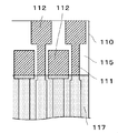
次に、本実施形態に係る電気光学装置が備えるフレキシブルコネクタについて、図5及び図6を参照して説明する。図5は、本実施形態に係る電気光学装置が備えるフレキシブルコネクタの構成を示す平面図であり、図6は、その変形例に係るフレキシブルコネクタの構成を示す平面図である。 Next, a flexible connector provided in the electro-optical device according to the present embodiment will be described with reference to FIGS. 5 and 6. FIG. 5 is a plan view showing the configuration of the flexible connector provided in the electro-optical device according to this embodiment, and FIG. 6 is a plan view showing the configuration of the flexible connector according to the modification.
図5において、フレキシブルコネクタ110は、フレキシブル配線基板115上に形成された、複数の外部回路接続端子102(図3参照)と接続するための複数の接続部112と、この複数の接続部112と外部回路とを接続するための複数の外部回路接続配線111と、複数の外部回路接続配線111を覆うように形成された絶縁膜117とから構成されている。そして、複数の接続部112は、複数の外部回路接続端子102(図3参照)の配置に対応して配置されている。即ち、隣接する複数の接続部112は、相互に配列方向と交わる方向(図5中、上下方向)にずれて配置され、配列方向に沿った2列として配列されている。
In FIG. 5, the
このように構成されているので、フレキシブルコネクタ110は、通常のフレキシブルコネクタとは異なり、複数の外部回路接続端子102(図3参照)の配置に対応して配置された複数の接続部112を持つ。従って、本実施形態に係る電気光学装置における特殊配列された複数の接続部112と外部回路との電気的な接続を、フレキシブルコネクタ110を介して良好にとることができる。
Since it is configured in this way, the
尚、絶縁膜117の複数の接続部112がある側の端部は、図5に示すように、複数の接続部112の配列方向(図3中、左右方向)に沿って真っ直ぐに形成されている必要はない。
The end of the insulating
例えば図6にその変形例として示すように、絶縁膜117の複数の接続部112がある側の端部を平面的に見て複数の接続部112に沿った形状とし、外部回路接続配線111を更に覆うようにしてもよい。このようにすれば、相隣接する複数の接続部112と複数の外部回路接続配線111との電気的ショートを防止することができる。
<第2実施形態>
第2実施形態に係る電気光学装置について、図7から図12を参照して説明する。第2実施形態は、外部回路接続端子102の平面レイアウト或いは平面パターンについての各種具体例に係る。
For example, as shown as a modified example in FIG. 6, the end of the insulating
Second Embodiment
An electro-optical device according to the second embodiment will be described with reference to FIGS. The second embodiment relates to various specific examples of the planar layout or planar pattern of the external
先ず、第2実施形態における一具体例について図7を参照して説明する。ここに図7は、第2実施形態の一具体例についての、第1実施形態における図4と同趣旨の拡大図である。尚、図7において、図1から図6に示した第1実施形態に係る構成要素と同様の構成要素に同一の参照符合を付し、それらの説明は適宜省略する。 First, a specific example in the second embodiment will be described with reference to FIG. FIG. 7 is an enlarged view having the same concept as FIG. 4 in the first embodiment, regarding a specific example of the second embodiment. In FIG. 7, the same reference numerals are given to the same components as those according to the first embodiment shown in FIGS. 1 to 6, and description thereof will be omitted as appropriate.
図7において、第2実施形態の一具体例に係る電気光学装置では、複数の外部回路接続端子102は夫々、複数の外部回路接続端子102の配列方向の幅ΔWが複数の外部回路接続端子の配列ピッチΔPよりも広い部分を含むと共に、TFTアレイ基板10上で平面的に見て相互に重ならない、形状を有する。より具体的には、複数の外部回路接続端子102は夫々三角形の形状を有し、隣接する外部回路接続端子102は相互に重なり合わないように若干の隙間を隔てて交互に上下逆転して配列されている。つまり、相隣接する二つの外部回路接続端子102は、平面的に見て相互間の隙間を実質的に一定幅とする形状或いは一定幅に近付ける形状、言い換えれば、相補的な形状を有する。
In the electro-optical device according to the specific example of the second embodiment in FIG. 7, the plurality of external
その他の構成については、上述した第1実施形態と同様の構成されている。 About another structure, it is the same structure as 1st Embodiment mentioned above.
以上のように、第2実施形態に係る電気光学装置の一具体例によれば、外部回路接続端子102個々の面積を確保しつつ外部回路接続端子102が配列された辺の長さを縮めることが可能となり、TFTアレイ基板10のサイズの縮小が可能となる。この際、相互間の隙間を実質的に一定幅とする形状或いは一定幅に近付ける形状、言い換えれば、相補的な形状を有する外部回路接続端子102が、相互に重なったり、相互にショートしたり、僅かな欠陥や製造誤差により相互にショートしたりすることを、殆どなくすことが可能となる。
As described above, according to the specific example of the electro-optical device according to the second embodiment, the length of the side where the external
本実施形態に係る複数の外部回路接続端子102の形状は、上述のように形成される一具体例以外に、図8から図11に他の各種具体例として示した如きであってもよい。ここに、図8から図11は夫々、第2実施形態の他の各種具体例についての、第1実施形態における図4と同趣旨の拡大図である。
The shapes of the plurality of external
即ち図8に他の具体例として示すように、複数の外部回路接続端子102は、若干の隙間を隔てて噛み合うような形状に、形成されていてもよい。また、例えば、平面的に見て、隣接する外部回路接続端子102間で、若干の隙間を隔てての入れ子状又は合符状に、或いは若干の隙間を隔てて係合又は噛み合うような形状に、形成されていてもよい。
That is, as shown in FIG. 8 as another specific example, the plurality of external
図9に他の具体例として示すように、複数の外部回路接続端子102は、それらの配列方向に沿って、それらの重心或いは中心が一直線に配列されている必要は無く、第1実施形態と同様に、配列方向に交差する方向にずれて配置されていてもよい。より具体的には、千鳥足状の形式で配列方向に交差する方向にずれて配置されていてもよい。
As shown in FIG. 9 as another specific example, the plurality of external
図10に他の具体例として示すように、円状の形式で配列方向に交差する方向にずれて配置されていてもよい。 As shown in FIG. 10 as another specific example, they may be arranged so as to be shifted in a direction intersecting the arrangement direction in a circular form.
或いは、図11に示すように八角形状の形式で、配列方向に交差する方向にずれて配置されていてもよい。 Alternatively, as shown in FIG. 11, they may be arranged in an octagonal form and shifted in a direction intersecting the arrangement direction.
このように構成された第2実施形態によれば、より効率的に外部回路接続端子102個々の面積を確保しつつ外部回路接続端子102が配列された辺の長さを縮めることが可能となる。
According to the second embodiment configured as described above, it is possible to reduce the length of the side on which the external
次に、図12を参照して、第2実施形態に係る電気光学装置が備えるフレキシブルコネクタ110について説明する。ここに図12は、図5及び図6と同趣旨の本実施形態に係るフレキシブルコネクタの構成を示す平面図である。
Next, the
即ち図12に示すように、第2実施形態に係る電気光学装置が備えるフレキシブルコネクタ110は、第1実施形態に係る電気光学装置が備えるフレキシブルコネクタ(図5参照)と同様、複数の外部回路接続端子102の形状に対応する形状を有する複数の接続部112を持つ。従って、第1実施形態と同様に、特殊配列された複数の接続部112と外部回路との電気的な接続を、フレキシブルコネクタ110を介して良好にとることが可能となる。
<変形例>
第1又は第2実施形態に係る電気光学装置の変形例について、図13を参照して説明する。ここに図13は、本変形例における、図3におけるS−S’断面図及びT−T’断面図である。尚、図13において、図1から図12に示した第1及び第2実施形態に係る構成要素と同様の構成要素に同一の参照符合を付し、それらの説明は適宜省略する。
That is, as shown in FIG. 12, the
<Modification>
A modification of the electro-optical device according to the first or second embodiment will be described with reference to FIG. FIG. 13 is an SS ′ sectional view and a TT ′ sectional view in FIG. 3 in this modification. In FIG. 13, the same components as those in the first and second embodiments shown in FIGS. 1 to 12 are denoted by the same reference numerals, and description thereof will be omitted as appropriate.
図13に示すように、本変形例に係る電気光学装置において、複数の外部回路接続端子102(図3参照)のうち外部回路接続端子102a及び102bは相隣接している。外部回路接続端子102aは、複数の引出配線140(図3参照)のうち第1導電膜から形成された第1引出配線140aに接続されており、外部回路接続端子102bは、層間絶縁膜43を介して第1導電膜と別層に位置する第2導電膜から形成された第2引出配線140bに接続されている。
As shown in FIG. 13, in the electro-optical device according to this modification, the external
より具体的には図13から分かるように、TFTアレイ基板10上には、順に、下地絶縁膜12、第1層間絶縁膜41、第2層間絶縁膜42、第3層間絶縁膜43、第4層間絶縁膜44が、この順に積層されている。第2層間絶縁膜42上に積層された第2の導電膜から、第2引出配線140bが形成されている。第3層間絶縁膜43上に積層された第1の導電膜から、第1引出配線140a及び外部回路接続端子102が夫々形成されている。層間絶縁膜43の表面は、例えばCMP(Chemical Mechanical Polishing:化学的機会研磨)等の平坦化処理が施されている。但し、このような平坦化処理が施されていなくても構わない。
More specifically, as can be seen from FIG. 13, on the
このようにTFTアレイ基板10上に、このように複数の層間絶縁膜及び導電膜が積層されているので、これらを利用して、更にこれらの層間に積層される他の導電膜や半導体膜等を利用して、TFT等の各種回路を、TFTアレイ基板10上における画像表示領域内に作り込むことが可能となり、これと同一又は別機会に、引出配線140及び外部回路接続端子102を作り込むことが可能となる。
As described above, since the plurality of interlayer insulating films and the conductive films are laminated on the
本変形例に係る電気光学装置は、外部回路接続端子102a及び102bと夫々接続される第1引出配線140a及び第2引出配線140は、本発明に係る「層間絶縁膜」の一例としての第3層間絶縁膜43を介して別層に位置する第1及び第2導電膜から夫々形成されている。よって、第1引出配線140aと第2引出配線140bとが、平面的に見て接近して配線されても、配線間ショートが生じる事態を効果的に防止することが可能となる。また、平面的に見て第1引出配線140a及び第2引出配線140bが重なる程度に、両者の配線幅を広くとることも可能となる。
In the electro-optical device according to this modification, the first lead-
特に本変形例では、外部回路接続端子102bは、第2引出配線140bに第3層間絶縁膜43に開孔されたコンタクトホール20bを介して電気的に接続されており、相隣接する二つの外部回路接続端子102a及び102bは共に、第1導電膜と同一の導電膜から形成されている。尚、相隣接する二つの外部回路接続端子102a及び102bは共に、第1導電膜と同一の導電膜から形成されてもよい。
In particular, in this modification, the external
よって、外部回路接続端子102については、同一導電膜から形成することで、フレキシブルコネクタ等の接続部が接続される表面の高さを揃えつつ、第1引出配線140a及び第2引出配線140bについては、二つの導電膜から形成することで、配線間ショートが生じる事態を防止することが可能となる。
<電子機器>
次に、上述した電気光学装置である液晶装置を各種の電子機器に適用する場合について説明する。
Therefore, by forming the external
<Electronic equipment>
Next, the case where the liquid crystal device which is the above-described electro-optical device is applied to various electronic devices will be described.
まず、この液晶装置をライトバルブとして用いたプロジェクタについて説明する。図14は、プロジェクタの構成例を示す平面図である。この図14に示されるように、プロジェクタ1100内部には、ハロゲンランプ等の白色光源からなるランプユニット1102が設けられている。このランプユニット1102から射出された投射光は、ライトガイド1104内に配置された4枚のミラー1106および2枚のダイクロイックミラー1108によってRGBの3原色に分離され、各原色に対応するライトバルブとしての液晶パネル1110R、1110Bおよび1110Gに入射される。
First, a projector using this liquid crystal device as a light valve will be described. FIG. 14 is a plan view showing a configuration example of the projector. As shown in FIG. 14, a
液晶パネル1110R、1110Bおよび1110Gの構成は、上述した液晶装置と同等であり、画像信号処理回路から供給されるR、G、Bの原色信号でそれぞれ駆動されるものである。そして、これらの液晶パネルによって変調された光は、ダイクロイックプリズム1112に3方向から入射される。このダイクロイックプリズム1112においては、RおよびBの光が90度に屈折する一方、Gの光が直進する。したがって、各色の画像が合成される結果、投射レンズ1114を介して、スクリーン等にカラー画像が投写されることとなる。
The configurations of the
ここで、各液晶パネル1110R、1110Bおよび1110Gによる表示像について着目すると、液晶パネル1110Gによる表示像は、液晶パネル1110R、1110Bによる表示像に対して左右反転することが必要となる。
Here, paying attention to the display images by the
なお、液晶パネル1110R、1110Bおよび1110Gには、ダイクロイックミラー1108によって、R、G、Bの各原色に対応する光が入射するので、カラーフィルタを設ける必要はない。
Note that since light corresponding to the primary colors R, G, and B is incident on the
次に、液晶装置を、モバイル型のパーソナルコンピュータに適用した例について説明する。図15は、このパーソナルコンピュータの構成を示す斜視図である。図15において、コンピュータ1200は、キーボード1202を備えた本体部1204と、液晶表示ユニット1206とから構成されている。この液晶表示ユニット1206は、先に述べた液晶装置1005の背面にバックライトを付加することにより構成されている。
Next, an example in which the liquid crystal device is applied to a mobile personal computer will be described. FIG. 15 is a perspective view showing the configuration of this personal computer. In FIG. 15, a
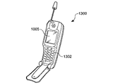
さらに、液晶装置を、携帯電話に適用した例について説明する。図16は、この携帯電話の構成を示す斜視図である。図16において、携帯電話1300は、複数の操作ボタン1302とともに、反射型の液晶装置1005を備えるものである。この反射型の液晶装置1005にあっては、必要に応じてその前面にフロントライトが設けられる。
Further, an example in which the liquid crystal device is applied to a mobile phone will be described. FIG. 16 is a perspective view showing the configuration of this mobile phone. In FIG. 16, a
尚、図14から図16を参照して説明した電子機器の他にも、液晶テレビや、ビューファインダ型、モニタ直視型のビデオテープレコーダ、カーナビゲーション装置、ページャ、電子手帳、電卓、ワードプロセッサ、ワークステーション、テレビ電話、POS端末、タッチパネルを備えた装置等などが挙げられる。そして、これらの各種電子機器に適用可能なのは言うまでもない。 In addition to the electronic devices described with reference to FIGS. 14 to 16, a liquid crystal television, a viewfinder type, a monitor direct view type video tape recorder, a car navigation device, a pager, an electronic notebook, a calculator, a word processor, a work Examples include a station, a videophone, a POS terminal, a device equipped with a touch panel, and the like. Needless to say, the present invention can be applied to these various electronic devices.
本発明は、上述した実施形態に限られるものではなく、請求の範囲及び明細書全体から読み取れる発明の要旨或いは思想に反しない範囲で適宜変更可能であり、そのような変更を伴う電気光学装置及び該電気光学装置を備えてなる電子機器もまた本発明の技術的範囲に含まれるものである。 The present invention is not limited to the above-described embodiments, and can be appropriately changed without departing from the spirit or concept of the invention that can be read from the claims and the entire specification. An electronic apparatus including the electro-optical device is also included in the technical scope of the present invention.
10…TFTアレイ基板、3a…走査線、6a…データ線、9a…画素電極、10a…画像表示領域、20…対向基板、21…対向電極、41、42、43、44…層間絶縁層、50…液晶層、52…シール材、53…額縁遮光膜、101…データ線駆動回路、102、102a、102b…外部回路接続端子、104…走査線駆動回路、106…上下導通端子、110…フレキシブルコネクタ、111…外部回路接続配線、112…接続部、115…フレキシブル配線基板、117…絶縁膜、120…走査線駆動用配線、130…データ線駆動用配線、140、140a、140b…引出配線、301…サンプリング回路
DESCRIPTION OF
Claims (12)
画像表示領域に配置された表示用電極と、
該表示用電極を駆動するための配線及び回路のうち少なくとも一方と、
該配線及び回路のうち少なくとも一方から、前記画像表示領域の周辺に位置する周辺領域に夫々引き出されている複数の引出配線と、
該複数の引出配線に夫々接続されており、前記周辺領域に配列された複数の外部回路接続端子と
を備え、
前記複数の外部回路接続端子は夫々、前記複数の外部回路接続端子の配列方向の幅が、前記複数の外部回路接続端子の配列ピッチよりも広い部分を含む形状を有し、
前記複数の外部回路接続端子は、前記基板上で平面的に見て相互に重ならないように、前記配列方向と交わる方向にずれて配置されている
ことを特徴とする電気光学装置。 On the board
Display electrodes arranged in the image display area;
At least one of wiring and circuit for driving the display electrode;
A plurality of lead wires each led out from at least one of the wires and circuits to a peripheral region located around the image display region;
A plurality of external circuit connection terminals respectively connected to the plurality of lead wires and arranged in the peripheral region;
Each of the plurality of external circuit connection terminals has a shape including a portion where the width in the arrangement direction of the plurality of external circuit connection terminals is wider than the arrangement pitch of the plurality of external circuit connection terminals,
The electro-optical device, wherein the plurality of external circuit connection terminals are shifted in a direction intersecting with the arrangement direction so as not to overlap each other when viewed in plan on the substrate.
画像表示領域に配置された表示用電極と、
該表示用電極を駆動するための配線及び回路のうち少なくとも一方と、
該配線及び回路のうち少なくとも一方から、前記画像表示領域の周辺に位置する周辺領域に夫々引き出されている複数の引出配線と、
該複数の引出配線に夫々接続されており、前記周辺領域に配列された複数の外部回路接続端子と
を備え、
前記複数の外部回路接続端子は夫々、前記複数の外部回路接続端子の配列方向の幅が前記複数の外部回路接続端子の配列ピッチよりも広い部分を含むと共に、前記基板上で平面的に見て相互に重ならない、形状を有する
ことを特徴とする電気光学装置。 On the board
Display electrodes arranged in the image display area;
At least one of wiring and circuit for driving the display electrode;
A plurality of lead wires each led to a peripheral region located around the image display region from at least one of the wires and circuits;
A plurality of external circuit connection terminals respectively connected to the plurality of lead wires and arranged in the peripheral region;
Each of the plurality of external circuit connection terminals includes a portion in which the width in the arrangement direction of the plurality of external circuit connection terminals is wider than the arrangement pitch of the plurality of external circuit connection terminals, and is viewed in plan on the substrate. An electro-optical device characterized by having shapes that do not overlap each other.
前記相隣接する二つの外部回路接続端子は共に、前記第1又は第2導電膜と同一の導電膜から形成されていることを特徴とする請求項8に記載の電気光学装置。 The other of the two adjacent external circuit connection terminals is electrically connected to the second lead wiring via a contact hole opened in the interlayer insulating film,
The electro-optical device according to claim 8, wherein the two adjacent external circuit connection terminals are formed of the same conductive film as the first or second conductive film.
画像表示領域に配置された表示用電極と、
該表示用電極を駆動するための配線及び回路のうち少なくとも一方と、
該配線及び回路のうち少なくとも一方から、前記画像表示領域の周辺に位置する周辺領域に夫々引き出されている複数の引出配線と、
該複数の引出配線に夫々接続されており、前記周辺領域に配列された複数の外部回路接続端子と
を備え、
前記複数の外部回路接続端子は夫々、前記複数の外部回路接続端子の配列方向の幅が前記複数の外部回路接続端子の配列ピッチよりも広い部分を含む形状を有し、
前記複数の外部回路接続端子は、前記基板上で平面的に見て相互に重ならないように、前記配列方向と交差する方向にずれて配置されていることを特徴とする電気光学装置用基板。 On the board
Display electrodes arranged in the image display area;
At least one of wiring and circuit for driving the display electrode;
A plurality of lead wires each led to a peripheral region located around the image display region from at least one of the wires and circuits;
A plurality of external circuit connection terminals respectively connected to the plurality of lead wires and arranged in the peripheral region;
Each of the plurality of external circuit connection terminals has a shape including a portion in which the width in the arrangement direction of the plurality of external circuit connection terminals is wider than the arrangement pitch of the plurality of external circuit connection terminals,
The substrate for an electro-optical device, wherein the plurality of external circuit connection terminals are shifted in a direction crossing the arrangement direction so as not to overlap each other when viewed in plan on the substrate.
画像表示領域に配置された表示用電極と、
該表示用電極を駆動するための配線及び回路のうち少なくとも一方と、
該配線及び回路のうち少なくとも一方から、前記画像表示領域の周辺に位置する周辺領域に夫々引き出されている複数の引出配線と、
該複数の引出配線に夫々接続されており、前記周辺領域に配列された複数の外部回路接続端子と
を備え、
前記複数の外部回路接続端子は夫々、前記複数の外部回路接続端子の配列方向の幅が前記複数の外部回路接続端子の配列ピッチよりも広い部分を含むと共に、前記基板上で平面的に見て相互に重ならない、形状を有することを特徴とする電気光学装置用基板。 On the board
Display electrodes arranged in the image display area;
At least one of wiring and circuit for driving the display electrode;
A plurality of lead wires each led to a peripheral region located around the image display region from at least one of the wires and circuits;
A plurality of external circuit connection terminals respectively connected to the plurality of lead wires and arranged in the peripheral region;
Each of the plurality of external circuit connection terminals includes a portion in which the width in the arrangement direction of the plurality of external circuit connection terminals is wider than the arrangement pitch of the plurality of external circuit connection terminals, and is viewed in plan on the substrate. A substrate for an electro-optical device having a shape that does not overlap with each other.
An electronic apparatus comprising the electro-optical device according to claim 1.
Priority Applications (1)
| Application Number | Priority Date | Filing Date | Title |
|---|---|---|---|
| JP2004370083A JP2006178113A (en) | 2004-12-21 | 2004-12-21 | Electro-optical device, substrate for the electro-optical device, and electronic apparatus |
Applications Claiming Priority (1)
| Application Number | Priority Date | Filing Date | Title |
|---|---|---|---|
| JP2004370083A JP2006178113A (en) | 2004-12-21 | 2004-12-21 | Electro-optical device, substrate for the electro-optical device, and electronic apparatus |
Publications (1)
| Publication Number | Publication Date |
|---|---|
| JP2006178113A true JP2006178113A (en) | 2006-07-06 |
Family
ID=36732291
Family Applications (1)
| Application Number | Title | Priority Date | Filing Date |
|---|---|---|---|
| JP2004370083A Pending JP2006178113A (en) | 2004-12-21 | 2004-12-21 | Electro-optical device, substrate for the electro-optical device, and electronic apparatus |
Country Status (1)
| Country | Link |
|---|---|
| JP (1) | JP2006178113A (en) |
Cited By (4)
| Publication number | Priority date | Publication date | Assignee | Title |
|---|---|---|---|---|
| JP2013190456A (en) * | 2012-03-12 | 2013-09-26 | Mitsubishi Electric Corp | Wiring structure, thin film transistor array substrate including the same, and display device |
| US9666607B2 (en) | 2013-01-31 | 2017-05-30 | Samsung Display Co., Ltd. | Display device |
| JP2017151575A (en) * | 2016-02-23 | 2017-08-31 | パナソニックIpマネジメント株式会社 | Touch sensor and electronic apparatus using the touch sensor |
| CN114170904A (en) * | 2021-12-06 | 2022-03-11 | 合肥维信诺科技有限公司 | Display module and display device |
-
2004
- 2004-12-21 JP JP2004370083A patent/JP2006178113A/en active Pending
Cited By (5)
| Publication number | Priority date | Publication date | Assignee | Title |
|---|---|---|---|---|
| JP2013190456A (en) * | 2012-03-12 | 2013-09-26 | Mitsubishi Electric Corp | Wiring structure, thin film transistor array substrate including the same, and display device |
| US9627585B2 (en) | 2012-03-12 | 2017-04-18 | Mitsubishi Electric Corporation | Wiring structure, thin film transistor array substrate including the same, and display device |
| US9666607B2 (en) | 2013-01-31 | 2017-05-30 | Samsung Display Co., Ltd. | Display device |
| JP2017151575A (en) * | 2016-02-23 | 2017-08-31 | パナソニックIpマネジメント株式会社 | Touch sensor and electronic apparatus using the touch sensor |
| CN114170904A (en) * | 2021-12-06 | 2022-03-11 | 合肥维信诺科技有限公司 | Display module and display device |
Similar Documents
| Publication | Publication Date | Title |
|---|---|---|
| JP4560026B2 (en) | Flexible substrate, electro-optical device including the same, and electronic apparatus | |
| JP2009075457A (en) | Electro-optical device, electro-optical device mounting case and electronic apparatus | |
| US20090059141A1 (en) | Electro-optic device, and electronic apparatus including the same | |
| JP5104176B2 (en) | Electro-optical device and electronic apparatus | |
| JP2008084968A (en) | Flexible board, electrochemical device with it and electronic equipment | |
| JP4992774B2 (en) | Electro-optical device and electronic apparatus | |
| JP2006259691A (en) | Electro-optical device, its manufacturing method and electronic apparatus | |
| JP2008090112A (en) | Flexible board, electrooptical device with the same and electronic device | |
| JP5292969B2 (en) | Electro-optical device and electronic apparatus including the same | |
| JP5500217B2 (en) | Electro-optical device and electronic apparatus | |
| JP2006178113A (en) | Electro-optical device, substrate for the electro-optical device, and electronic apparatus | |
| JP4747572B2 (en) | Electro-optical device and electronic apparatus | |
| JP5532944B2 (en) | Electro-optical device substrate, electro-optical device, and electronic apparatus | |
| JP4858021B2 (en) | Electro-optical device and electronic apparatus | |
| JP5590050B2 (en) | Electro-optical device and electronic apparatus | |
| JP4946740B2 (en) | WIRING BOARD, ELECTRO-OPTICAL DEVICE HAVING THE WIRING BOARD, AND ELECTRONIC DEVICE | |
| JP5124974B2 (en) | Electro-optical device and electronic apparatus including the same | |
| JP6287252B2 (en) | Electro-optical device and electronic apparatus | |
| JP4639789B2 (en) | Electro-optical device and electronic apparatus | |
| JP2014206595A (en) | Liquid crystal display device | |
| JP5104156B2 (en) | ELECTRO-OPTICAL DEVICE AND ELECTRONIC DEVICE HAVING THE SAME | |
| JP2005181399A (en) | Electrooptic device and electronic equipment | |
| JP5664721B2 (en) | Electro-optical device and electronic apparatus | |
| JP2008040290A (en) | Electrooptical device and electronic equipment | |
| JP2009116089A (en) | Electro-optical device and electronic apparatus |