JP2006128576A - Electrolytic processing apparatus and method therefor - Google Patents
Electrolytic processing apparatus and method therefor Download PDFInfo
- Publication number
- JP2006128576A JP2006128576A JP2004318380A JP2004318380A JP2006128576A JP 2006128576 A JP2006128576 A JP 2006128576A JP 2004318380 A JP2004318380 A JP 2004318380A JP 2004318380 A JP2004318380 A JP 2004318380A JP 2006128576 A JP2006128576 A JP 2006128576A
- Authority
- JP
- Japan
- Prior art keywords
- electrode
- workpiece
- processing
- feeding
- machining
- Prior art date
- Legal status (The legal status is an assumption and is not a legal conclusion. Google has not performed a legal analysis and makes no representation as to the accuracy of the status listed.)
- Withdrawn
Links
Images


Abstract
Description
本発明は、電解加工装置及び電解加工方法に係り、特に半導体ウエハ等の基板の表面に形成された導電性材料を加工したり、基板の表面に付着した不純物を除去したりするのに使用される電解加工装置及び電解加工方法に関する。 The present invention relates to an electrolytic processing apparatus and an electrolytic processing method, and is particularly used for processing a conductive material formed on the surface of a substrate such as a semiconductor wafer or removing impurities adhering to the surface of the substrate. The present invention relates to an electrolytic processing apparatus and an electrolytic processing method.
近年、半導体ウエハ等の基板上に回路を形成するための配線材料として、アルミニウムまたはアルミニウム合金に代えて、電気抵抗率が低くエレクトロマイグレーション耐性が高い銅(Cu)を用いる動きが顕著になっている。この種の銅配線は、基板の表面に設けた微細凹みの内部に銅を埋め込むことによって一般に形成される。この銅配線を形成する方法としては、化学気相成長法(CVD)、スパッタリング及びめっきといった手法があるが、いずれにしても、基板のほぼ全表面に銅を成膜して、化学機械的研磨(CMP)により不要の銅を除去するようにしている。 In recent years, as a wiring material for forming a circuit on a substrate such as a semiconductor wafer, the movement of using copper (Cu) having low electrical resistivity and high electromigration resistance instead of aluminum or an aluminum alloy has become prominent. . This type of copper wiring is generally formed by embedding copper in a fine recess provided on the surface of the substrate. Methods for forming this copper wiring include chemical vapor deposition (CVD), sputtering, and plating, but in any case, copper is deposited on almost the entire surface of the substrate, and chemical mechanical polishing is performed. Unnecessary copper is removed by (CMP).
図1(a)乃至図1(c)は、この種の銅配線基板Wの一製造例を工程順に示す。先ず、図1(a)に示すように、半導体素子が形成された半導体基材1上の導電層1aの上にSiO2からなる酸化膜やLow−k材膜などの絶縁膜2が堆積され、リソグラフィ・エッチング技術によりコンタクトホール3と配線溝4が形成される。これらの上にTaN等からなるバリア膜5、更にその上に電解めっきの給電層としてのシード層7がスパッタリングやCVD等により形成される。
FIG. 1A to FIG. 1C show a manufacturing example of this type of copper wiring board W in the order of steps. First, as shown in FIG. 1A, an
そして、基板Wの表面に銅めっきを施すことで、図1(b)に示すように、半導体基板Wのコンタクトホール3及び配線溝4内に銅を充填するとともに、絶縁膜2上に銅膜6を堆積する。その後、化学機械的研磨(CMP)により、絶縁膜2上の銅膜6、シード層7及びバリア膜5を除去して、コンタクトホール3及び配線溝4内に充填させた銅膜6の表面と絶縁膜2の表面とをほぼ同一平面にする。これにより、図1(c)に示すように、絶縁膜2の内部に銅膜6からなる配線が形成される。
Then, by copper plating on the surface of the substrate W, the
最近ではあらゆる機器の構成要素において微細化かつ高精度化が進み、サブミクロン領域での物作りが一般的となるにつれて、加工法自体が材料の特性に与える影響は益々大きくなっている。このような状況下においては、従来の機械加工のように、工具が被加工物を物理的に破壊しながら除去していく加工方法では、加工によって被加工物に多くの欠陥を生み出してしまうため、被加工物の特性が劣化してしまう。したがって、いかに材料の特性を損なうことなく加工を行うことができるかが問題となってくる。 In recent years, as the miniaturization and high precision have progressed in the components of all devices, and the manufacturing in the sub-micron region has become common, the influence of the processing method itself on the characteristics of the material has been increasing. Under such circumstances, the machining method in which the tool removes the workpiece while physically destroying it, as in conventional machining, because many defects are generated in the workpiece by machining. As a result, the properties of the workpiece are deteriorated. Therefore, it becomes a problem how the processing can be performed without impairing the characteristics of the material.
この問題を解決する手段として開発された特殊加工法に、化学研磨や電解加工、電解研磨がある。これらの加工方法は、従来の物理的な加工とは対照的に、化学的溶解反応を起こすことによって、除去加工等を行うものである。したがって、塑性変形による加工変質層や転位等の欠陥は発生せず、上述の材料の特性を損なわずに加工を行うといった課題が達成される。 Special processing methods developed as means for solving this problem include chemical polishing, electrolytic processing, and electrolytic polishing. In contrast to conventional physical processing, these processing methods perform removal processing and the like by causing a chemical dissolution reaction. Therefore, defects such as work-affected layers and dislocations due to plastic deformation do not occur, and the problem of performing processing without impairing the properties of the above-described materials is achieved.
例えば、CMP工程は、一般にかなり複雑な操作が必要で、制御も複雑となり、加工時間もかなり長い。更に、研磨後の基板の後洗浄を十分に行う必要があるばかりでなく、スラリーや洗浄液の排液処理のための負荷が大きい等の課題がある。このため、CMP自体を省略もしくはこの負荷を軽減することが強く求められていた。また、今後、層間絶縁膜も誘電率の小さいLow−k材に変わると予想され、そのLow−k材は、機械的強度が弱くCMPによるストレスに耐えられなくなる。従って、基板にストレスを与えることなく、平坦化できるようにしたプロセスが望まれている。 For example, the CMP process generally requires a considerably complicated operation, is complicated in control, and has a considerably long processing time. Furthermore, not only is it necessary to sufficiently perform post-cleaning of the substrate after polishing, but there are also problems such as a large load for draining the slurry and cleaning liquid. For this reason, there has been a strong demand to omit CMP itself or reduce this load. In the future, the interlayer insulating film is also expected to change to a low-k material having a low dielectric constant, and the low-k material has low mechanical strength and cannot withstand stress caused by CMP. Therefore, there is a demand for a process that enables planarization without applying stress to the substrate.
このような課題を解決する手段として、電解液として純水もしくは超純水のような電気抵抗の大きな液体を用い、電極と被加工物の間に、必要に応じて、液体中の水分子の水酸化物イオンと水素イオンへの解離反応を促進するイオン交換体を配置して加工を行うことで、被加工物に与える機械的ストレスをなくし、後洗浄も簡便な電解加工が提案されている(例えば、特許文献1参照)。 As a means for solving such a problem, a liquid having a large electric resistance such as pure water or ultrapure water is used as an electrolytic solution, and water molecules in the liquid may be interposed between the electrode and the workpiece as necessary. Electrochemical machining that eliminates mechanical stress on the workpiece and facilitates post-cleaning by arranging an ion exchanger that promotes the dissociation reaction between hydroxide ions and hydrogen ions has been proposed. (For example, refer to Patent Document 1).
また、電解液を用いた電解加工(エッチング)において、被加工物と対向電極との距離を、特に10μm以下、例えば1μmに保ってエッチングを行うことで、処理後の被加工物表面の平坦性を向上させるようにしたもの(例えば、特許文献2参照)や、プラテン電極とウエハ(基板)の表面との距離を1mm以下、好ましくは2000Åにし、プラテン電極とウエハとの間に研磨パッド(厚み約200Å)をウエハ表面に接触させつつ介在させて、ウエハ表面を研磨するようにしたもの(例えば、特許文献3参照)等が提案されている。 Further, in electrolytic processing (etching) using an electrolytic solution, the surface of the workpiece after processing is flattened by performing etching while keeping the distance between the workpiece and the counter electrode at 10 μm or less, for example, 1 μm. The distance between the platen electrode and the surface of the wafer (substrate) is 1 mm or less, preferably 2000 mm, and a polishing pad (thickness) is provided between the platen electrode and the wafer. There has been proposed an apparatus in which the surface of the wafer is polished by bringing about 200 mm) into contact with the surface of the wafer (see, for example, Patent Document 3).
半導体ウエハ等の基板の表面に形成した、表面に凹凸のある導電性膜、例えば図1(b)に示す配線溝等の内部に埋込んだ銅膜6の不要な部分を、電解液を用いた電解加工で除去するのに際し、代表的な問題に導電性膜表面の凹凸の平坦化が困難であることが挙げられる。これは、(1)被加工物と電極との間の距離が基板表面に形成した導電性膜表面の凹凸段差よりも非常に大きいこと、(2)電解液の電気抵抗率が小さいこと、により導電性膜表面の凹部と凸部において、適切な加工速度差が得られないためである。また、特に基板等の被加工物と電極との間にイオン交換体が配置されている場合、一般にイオン交換体を被加工物表面に沿って摺動させながら電解加工が進行する。このため、このイオン交換体と被加工物表面との間の摺動に伴って、被加工物表面に欠陥が発生したり、イオン交換体が磨耗したりすることが問題となる。従って、電解加工を半導体ウエハ等の基板の表面に設けた導電性膜の除去に応用するには、このような問題を解決することが求められる。
An unnecessary portion of a conductive film having an uneven surface formed on the surface of a substrate such as a semiconductor wafer, for example, a
本発明は、上記事情に鑑みて為されたもので、被加工物表面の汚染や欠陥の発生を極力低減しつつ該表面をより平坦に加工できるようにした電解加工装置及び電解加工方法を提供することを目的とする。 The present invention has been made in view of the above circumstances, and provides an electrolytic processing apparatus and an electrolytic processing method capable of processing the surface more flat while reducing the occurrence of contamination and defects on the surface of the workpiece as much as possible. The purpose is to do.
請求項1に記載の発明は、被加工物に近接自在な加工電極と、前記被加工物に給電する給電電極と、前記加工電極と前記給電電極との間に電圧を印加する電源と、前記被加工物と前記加工電極または前記給電電極の少なくとも一方とを相対運動させる駆動部と、前記被加工物と前記加工電極または前記給電電極の少なくとも一方との間に液体を供給する液体供給部と、前記被加工物と前記加工電極または前記給電電極の少なくとも一方との距離を検出する検出器と、前記検出器からの信号を基に前記被加工物と前記加工電極または前記給電電極の少なくとも一方との距離を100μm以下で互いに非接触な所定値に制御する制御部を有することを特徴とする電解加工装置である。
The invention described in
被加工物と加工電極または給電電極の少なくとも一方との距離を100μm以下で互いに非接触な所定値に制御しつつ加工を行うことで、例えば半導体ウエハ等の基板の表面に形成された導電性膜の表面に、例えば段差が200nm程度の凹凸があっても、この凹凸段差の凹部と凸部で電気抵抗差、ひいては加工速度差を生じさせて、凹凸を平坦に加工することができる。この被加工物と加工電極または給電電極の少なくとも一方との距離は、50μm以下であることが好ましく、10μm以下、更には1μm以下であることがより好ましい。 Conductive film formed on the surface of a substrate such as a semiconductor wafer by performing processing while controlling the distance between the workpiece and at least one of the processing electrode or the feeding electrode to a predetermined value that is 100 μm or less and non-contacting each other For example, even if there are irregularities with a level difference of about 200 nm on the surface, it is possible to process the irregularities flatly by causing a difference in electrical resistance and a processing speed difference between the concave and convex portions of the irregularity level difference. The distance between the workpiece and at least one of the processing electrode or the feeding electrode is preferably 50 μm or less, more preferably 10 μm or less, and even more preferably 1 μm or less.
被加工物と加工電極または給電電極の少なくとも一方との距離を検出する検出器としては、例えば光学式(反射式)や渦電流式の距離センサが使用される。電解加工のエンドポイントを検出する、いわゆるエンドポイントセンサを備えている場合には、エンドポイントセンサにこの検出器としての役割を併用させても良く、この場合、導電性膜等の膜厚と、被加工物と加工電極または給電電極の少なくとも一方との距離とを単一のセンサ(エンドポイントセンサ)で同時に計測することができる。 As a detector for detecting the distance between the workpiece and at least one of the processing electrode or the feeding electrode, for example, an optical (reflection type) or eddy current type distance sensor is used. In the case of providing a so-called end point sensor that detects an end point of electrolytic processing, the end point sensor may be used in combination with the role of this detector. The distance between the workpiece and at least one of the processing electrode or the feeding electrode can be simultaneously measured by a single sensor (endpoint sensor).
請求項2に記載の発明は、被加工物に近接自在な加工電極と、前記被加工物に給電する給電電極と、前記加工電極と前記給電電極との間に電圧を印加する電源と、前記被加工物と前記加工電極または前記給電電極の少なくとも一方とを相対運動させる駆動部と、前記被加工物と前記加工電極または前記給電電極の少なくとも一方との間に液体を供給する液体供給部と、前記被加工物と前記加工電極または前記給電電極の少なくとも一方との間に配置されるイオン交換体と、前記被加工物と前記イオン交換体との距離を検出する検出器と、前記検出器からの信号を基に前記被加工物と前記イオン交換体との距離を100μm以下で互いに非接触な所定値に制御する制御部を有することを特徴とする電解加工装置である。
The invention according to
このように、イオン交換体を備えることで、液体中の水分子の水酸化物イオンと水素イオンへの解離反応を促進させることができる。また、被加工物とイオン交換体との距離を100μm以下で互いに非接触な所定値に制御しつつ加工を行うことで、例えば半導体ウエハ等の基板の表面に形成された導電性膜の表面に、例えば段差が200nm程度の凹凸があっても、この凹凸段差の凹部と凸部で電気抵抗差、ひいては加工速度差を生じさせて凹凸を平坦化し、しかもイオン交換体と被加工物表面とを互いに摺動させることなく電解加工を行うことで、被加工物表面に欠陥が発生したり、イオン交換体が磨耗したりするのを防止することができる。この被加工物とイオン交換体との距離は、50μm以下であることが好ましく、10μm以下、更には1μm以下であることがより好ましい。 Thus, by providing an ion exchanger, the dissociation reaction of water molecules in the liquid into hydroxide ions and hydrogen ions can be promoted. Further, by performing processing while controlling the distance between the workpiece and the ion exchanger to a predetermined value that is 100 μm or less and non-contact with each other, the surface of the conductive film formed on the surface of the substrate such as a semiconductor wafer is formed. For example, even if there are irregularities with a level difference of about 200 nm, the concave and convex portions of this irregularity level difference cause a difference in electrical resistance, and thus a difference in processing speed, thereby flattening the irregularities, and the ion exchanger and workpiece surface By performing electrolytic processing without sliding each other, it is possible to prevent defects on the surface of the workpiece and wear of the ion exchanger. The distance between the workpiece and the ion exchanger is preferably 50 μm or less, more preferably 10 μm or less, and even more preferably 1 μm or less.
請求項3に記載の発明は、前記被加工物を前記加工電極または前記給電電極の少なくとも一方に接離する方向に移動自在にフローティング支持する保持部を有することを特徴とする請求項1または2記載の電解加工装置である。
これにより、電解加工の際に液体を介して被加工物に加えられる力の大きさに応じて、加工電極または前記給電電極の少なくとも一方に接離する方向に被加工物を容易に移動させて、被加工物と加工電極または前記給電電極の少なくとも一方との距離を調整することができる。
According to a third aspect of the present invention, there is provided a holding portion for floatingly supporting the workpiece so as to be movable in a direction in which it is in contact with or separated from at least one of the processing electrode or the power feeding electrode. It is an electrolytic processing apparatus of description.
Accordingly, the workpiece can be easily moved in a direction in which it is in contact with or separated from at least one of the machining electrode or the feeding electrode, depending on the magnitude of the force applied to the workpiece via the liquid during the electrolytic machining. The distance between the workpiece and at least one of the processing electrode and the feeding electrode can be adjusted.
請求項4に記載の発明は、前記制御部は、前記被加工物と前記加工電極または前記給電電極の少なくとも一方との間に供給される液体の圧力、前記被加工物と前記加工電極または前記給電電極の少なくとも一方との間の相対運動速度、または前記加工電極と前記給電電極との間に印加される電圧の少なくとも1つを制御することを特徴とする請求項1乃至3のいずれかに記載の電解加工装置である。
被加工物と加工電極または給電電極の少なくとも一方との間の相対運動速度を制御することで、この相対運動により発生するハイドロプレーニング現象による液体力(動圧)を介して、電解加工の際に液体を介して被加工物に加えられる力の大きさを制御することができる。
According to a fourth aspect of the present invention, the control unit is configured such that the pressure of the liquid supplied between the workpiece and at least one of the machining electrode or the feeding electrode, the workpiece and the machining electrode, or the The relative movement speed between at least one of the power supply electrodes or at least one of the voltages applied between the processing electrode and the power supply electrode is controlled. It is an electrolytic processing apparatus of description.
By controlling the relative motion speed between the workpiece and at least one of the processing electrode or the feeding electrode, the liquid force (dynamic pressure) due to the hydroplaning phenomenon generated by this relative motion can be used during the electrolytic processing. The magnitude of the force applied to the workpiece via the liquid can be controlled.
イオン交換体を備えた電解加工装置で電解加工を行うと、被加工物とイオン交換体との間に吸着力が作用し、この吸着力は、加工電極と給電電極との間に印加する電圧に影響を受ける。このため、加工電極と給電電極との間に印加する電圧を制御することで、被加工物とイオン交換体との距離を、両者の間に作用する吸着力を介して制御することができる。 When electrolytic processing is performed with an electrolytic processing apparatus equipped with an ion exchanger, an adsorption force acts between the workpiece and the ion exchanger, and this adsorption force is a voltage applied between the machining electrode and the feeding electrode. Affected by. For this reason, by controlling the voltage applied between the machining electrode and the feeding electrode, the distance between the workpiece and the ion exchanger can be controlled via the adsorption force acting between the two.
請求項5に記載の発明は、被加工物に近接自在な加工電極と、前記被加工物に給電する給電電極と、前記加工電極と前記給電電極との間に電圧を印加する電源と、前記被加工物と前記加工電極または前記給電電極の少なくとも一方とを相対運動させる駆動部と、前記被加工物と前記加工電極または前記給電電極の少なくとも一方との間に液体を供給する液体供給部と、前記被加工物と前記加工電極または前記給電電極の少なくとも一方との間に配置される厚さが100μm以下の絶縁スペーサを有することを特徴とする電解加工装置である。 According to a fifth aspect of the present invention, there is provided a machining electrode that is freely accessible to a workpiece, a feeding electrode that feeds power to the workpiece, a power source that applies a voltage between the machining electrode and the feeding electrode, A drive unit that relatively moves the workpiece and at least one of the machining electrode or the power feeding electrode; and a liquid supply unit that supplies liquid between the workpiece and at least one of the machining electrode or the power feeding electrode; An electrolytic processing apparatus comprising an insulating spacer having a thickness of 100 μm or less disposed between the workpiece and at least one of the processing electrode or the feeding electrode.
被加工物と加工電極または給電電極の少なくとも一方との間に厚さが100μm以下の絶縁スペーサを配置することで、被加工物と加工電極または給電電極の少なくとも一方との距離を、互いに非接触な100μm以下にすることができる。この絶縁スペーサの厚さは、50μm以下であることが好ましく、10μm以下、更には1μm以下であることがより好ましい。 By disposing an insulating spacer having a thickness of 100 μm or less between the workpiece and at least one of the machining electrode or the feeding electrode, the distance between the workpiece and at least one of the machining electrode or the feeding electrode is not in contact with each other. 100 μm or less. The thickness of the insulating spacer is preferably 50 μm or less, more preferably 10 μm or less, and even more preferably 1 μm or less.
請求項6に記載の発明は、被加工物に近接自在な加工電極と、前記被加工物に給電する給電電極と、前記加工電極と前記給電電極との間に電圧を印加する電源と、前記被加工物と前記加工電極または前記給電電極の少なくとも一方とを相対運動させる駆動部と、前記被加工物と前記加工電極または前記給電電極の少なくとも一方との間に液体を供給する液体供給部と、前記被加工物と前記加工電極または前記給電電極の少なくとも一方との間に配置されるイオン交換体と、前記被加工物と前記イオン交換体との間に配置される厚さが100μm以下の絶縁スペーサを有することを特徴とする電解加工装置である。 According to a sixth aspect of the present invention, there is provided a machining electrode that is close to a workpiece, a feeding electrode that feeds power to the workpiece, a power source that applies a voltage between the machining electrode and the feeding electrode, A drive unit that relatively moves the workpiece and at least one of the machining electrode or the power feeding electrode; and a liquid supply unit that supplies liquid between the workpiece and at least one of the machining electrode or the power feeding electrode; The ion exchanger disposed between the workpiece and at least one of the processing electrode or the feeding electrode, and the thickness disposed between the workpiece and the ion exchanger is 100 μm or less. An electrolytic processing apparatus having an insulating spacer.
被加工物と加工電極または給電電極の少なくとも一方との間に配置されるイオン交換体と、被加工物との間に厚さが100μm以下の絶縁スペーサを配置することで、イオン交換体と被加工物との間の距離を、互いに非接触な100μm以下にすることができる。 By disposing an ion exchanger disposed between the workpiece and at least one of the processing electrode or the feeding electrode and an insulating spacer having a thickness of 100 μm or less between the workpiece and the workpiece, The distance between the workpieces can be set to 100 μm or less without contact with each other.
請求項7に記載の発明は、前記絶縁スペーサは、多孔質材料からなることを特徴とする請求項5または6記載の電解加工装置である。
これにより、絶縁スペーサの通水性を確保して、液体が絶縁スペーサ内部を流通するようにすることができる。
The invention according to
Thereby, the water permeability of an insulating spacer can be ensured and a liquid can distribute | circulate the inside of an insulating spacer.
請求項8に記載の発明は、前記液体供給部は、前記被加工物と前記加工電極または前記給電電極の少なくとも一方との間に、液体の噴流が前記被加工物に衝突する方向、または側方の少なくとも一方から液体を供給することを特徴とする請求項1乃至7のいずれかに記載の電解加工装置である。
According to an eighth aspect of the present invention, in the liquid supply section, a direction or a side in which a liquid jet collides with the workpiece between the workpiece and at least one of the machining electrode or the feeding electrode. The electrolytic processing apparatus according to
前記液体は、超純水、純水または電気伝導度が500μS/em以下の液体であることが好ましい。
超純水は、例えば電気伝導度(1atm,25℃換算、以下同じ)が0.1μS/cm以下の水であり、純水は、電気伝導度が10μS/cm以下の水である。電気伝導度が大きい液体を使用すると、距離比から生じる抵抗比は同じだが、液体の抵抗値そのものが小さくなり、このため、例えば表面に凹凸がある導電性膜における凹部と凸部での抵抗差は小さくなって、凹凸の選択性があまり得られない。一方、超純水や純水を使用すると、距離の違いによる抵抗差も大きいので、凹凸の選択性はより良くなる。このため、液体として、超純水、純水または電気伝導度が500μS/cm以下の液体を使用することが望ましい。
The liquid is preferably ultrapure water, pure water, or a liquid having an electric conductivity of 500 μS / em or less.
Ultrapure water is, for example, water having an electric conductivity (1 atm, converted at 25 ° C., the same shall apply hereinafter) of 0.1 μS / cm or less, and pure water is water having an electric conductivity of 10 μS / cm or less. When a liquid with high electrical conductivity is used, the resistance ratio resulting from the distance ratio is the same, but the resistance value of the liquid itself is small. For this reason, for example, the resistance difference between the concave and convex portions in a conductive film with irregularities on the surface Becomes small, and the selectivity of the unevenness is not obtained so much. On the other hand, when ultrapure water or pure water is used, since the resistance difference due to the difference in distance is large, the selectivity of the unevenness is improved. For this reason, it is desirable to use ultrapure water, pure water, or a liquid having an electric conductivity of 500 μS / cm or less as the liquid.
請求項9に記載の発明は、被加工物に近接自在な加工電極と被加工物に給電する給電電極を用意し、前記被加工物と前記加工電極または前記給電電極の少なくとも一方との距離を100μm以下で互いに非接触な所定値に保持しながら、前記被加工物と前記加工電極または前記給電電極の少なくとも一方を液体の存在下で相対運動させ、前記加工電極と前記給電電極との間に電圧を印加することを特徴とする電解加工方法である。 According to a ninth aspect of the present invention, there is provided a machining electrode that is freely accessible to a workpiece and a feeding electrode that feeds power to the workpiece, and sets a distance between the workpiece and at least one of the machining electrode or the feeding electrode. While maintaining a predetermined value that is 100 μm or less and non-contact with each other, the workpiece and at least one of the processing electrode or the feeding electrode are relatively moved in the presence of a liquid, and between the processing electrode and the feeding electrode. An electrolytic processing method is characterized by applying a voltage.
請求項10に記載の発明は、前記被加工物と前記加工電極または前記給電電極の少なくとも一方との間に供給される液体の圧力により、前記被加工物と前記加工電極または前記給電電極の少なくとも一方との距離を100μm以下で互いに非接触な所定値に保持することを特徴とする請求項9記載の電解加工方法である。 According to a tenth aspect of the present invention, at least one of the workpiece and the processing electrode or the feeding electrode is caused by a pressure of a liquid supplied between the workpiece and at least one of the processing electrode or the feeding electrode. 10. The electrolytic processing method according to claim 9, wherein the distance from one side is maintained at a predetermined value which is 100 μm or less and is not in contact with each other.
請求項11に記載の発明は、前記被加工物と前記加工電極または前記給電電極の少なくとも一方との間の相対運動で発生する液体の圧力により、前記被加工物と前記加工電極または前記給電電極の少なくとも一方との距離を100μm以下で互いに非接触な所定値に保持することを特徴とする請求項9記載の電解加工方法である。 According to an eleventh aspect of the present invention, the workpiece, the machining electrode, or the feeding electrode is generated by a pressure of a liquid generated by a relative motion between the workpiece and at least one of the machining electrode or the feeding electrode. 10. The electrolytic processing method according to claim 9, wherein the distance between at least one of the two is maintained at a predetermined value that is 100 μm or less and is not in contact with each other.
請求項12に記載の発明は、被加工物に近接自在な加工電極と被加工物に給電する給電電極を用意し、前記被加工物と前記加工電極または前記給電電極の少なくとも一方との間にイオン交換体を配置し、前記被加工物と前記イオン交換体との距離を100μm以下で互いに非接触な所定値に保持しながら、前記被加工物と前記加工電極または前記給電電極の少なくとも一方とを液体の存在下で相対運動させ、前記加工電極と前記給電電極との間に電圧を印加することを特徴とする電解加工方法である。 According to a twelfth aspect of the present invention, a machining electrode that is close to the workpiece and a feeding electrode that feeds the workpiece are prepared, and the workpiece and at least one of the machining electrode or the feeding electrode are provided. An ion exchanger is disposed, and the workpiece and at least one of the machining electrode and the feeding electrode are held while maintaining a predetermined distance between the workpiece and the ion exchanger at 100 μm or less and non-contact with each other. Is subjected to relative movement in the presence of a liquid, and a voltage is applied between the machining electrode and the feeding electrode.
請求項13に記載の発明は、前記被加工物と前記加工電極または前記給電電極の少なくとも一方との間に存在する液体の圧力により、前記被加工物と前記イオン交換体との距離を100μm以下で互いに非接触な所定値に保持することを特徴とする請求項12記載の電解加工方法である。 According to a thirteenth aspect of the present invention, the distance between the workpiece and the ion exchanger is 100 μm or less due to the pressure of the liquid existing between the workpiece and at least one of the processing electrode or the feeding electrode. The electrolytic processing method according to claim 12, wherein the predetermined values are not in contact with each other.
請求項14に記載の発明は、前記被加工物と前記加工電極または前記給電電極の少なくとも一方との間の相対運動で発生する圧力により、前記被加工物と前記イオン交換体との距離を100μm以下で互いに非接触な所定値に保持することを特徴とする請求項13記載の電解加工方法である。
請求項15に記載の発明は、前記相対運動は、回転運動、並進運動、直線運動、スクロール運動または往復運動のいずれか、またはそれらの組合せであり、相対運動速度は、0.1m/s以上であることを特徴とする請求項11乃至14のいずれかに記載の電解加工方法である。
この相対運動速度は、1m/s以上であることが好ましく、2m/s以上であることが更に好ましい。
According to a fourteenth aspect of the present invention, a distance between the workpiece and the ion exchanger is set to 100 μm by a pressure generated by a relative motion between the workpiece and at least one of the processing electrode or the feeding electrode. The electrolytic processing method according to claim 13, wherein the predetermined values that are not in contact with each other are maintained below.
In the invention described in claim 15, the relative motion is any one of a rotational motion, a translational motion, a linear motion, a scroll motion and a reciprocating motion, or a combination thereof, and the relative motion speed is 0.1 m / s or more. 15. The electrolytic processing method according to claim 11, wherein the electrolytic processing method is any one of the following.
The relative motion speed is preferably 1 m / s or more, and more preferably 2 m / s or more.
請求項16に記載の発明は、被加工物に近接自在な加工電極と被加工物に給電する給電電極を用意し、前記被加工物と前記加工電極または前記給電電極の少なくとも一方との間に厚さが100μm以下の絶縁スペーサを配置し、前記被加工物と前記加工電極または前記給電電極の少なくとも一方とを液体の存在下で前記絶縁スペーサに互いに接触させつつ相対運動させ、前記加工電極と前記給電電極との間に電圧を印加することを特徴とする電解加工方法である。 According to a sixteenth aspect of the present invention, there is provided a machining electrode that is freely accessible to a workpiece and a feeding electrode that feeds power to the workpiece, and is provided between the workpiece and at least one of the machining electrode or the feeding electrode. An insulating spacer having a thickness of 100 μm or less is disposed, and the workpiece and at least one of the processing electrode or the feeding electrode are moved relative to each other in contact with the insulating spacer in the presence of a liquid, and the processing electrode and In the electrolytic processing method, a voltage is applied between the power supply electrode.
請求項17に記載の発明は、被加工物に近接自在な加工電極と被加工物に給電する給電電極を用意し、前記被加工物と前記加工電極または前記給電電極の少なくとも一方との間にイオン交換体を配置し、前記被加工物と前記イオン交換体との間に厚さが100μm以下の絶縁スペーサをイオン交換体に接触させて配置し、前記被加工物と前記加工電極または前記給電電極の少なくとも一方を液体の存在下で前記絶縁スペーサと前記イオン交換体に互いに接触させつつ相対運動させ、前記加工電極と前記給電電極との間に電圧を印加することを特徴とする電解加工方法である。 According to a seventeenth aspect of the present invention, there is provided a machining electrode that is freely accessible to a workpiece and a feeding electrode that feeds power to the workpiece, and is provided between the workpiece and at least one of the machining electrode or the feeding electrode. An ion exchanger is disposed, and an insulating spacer having a thickness of 100 μm or less is disposed between the workpiece and the ion exchanger in contact with the ion exchanger, and the workpiece and the processing electrode or the power supply are disposed. Electrolytic machining method characterized in that at least one of electrodes is moved relative to each other while being in contact with said insulating spacer and said ion exchanger in the presence of a liquid, and a voltage is applied between said machining electrode and said feeding electrode It is.
請求項18に記載の発明は、前記絶縁スペーサは、多孔質材料からなることを特徴とする請求項16または17記載の電解加工方法である。
請求項19に記載の発明は、前記被加工物と前記加工電極または前記給電電極の少なくとも一方との間に、液体の噴流が前記被加工物に衝突する方向、または側方の少なくとも一方から液体を供給することを特徴とする請求項9乃至18のいずれかに記載の電解加工方法である。
The invention according to claim 18 is the electrolytic processing method according to claim 16 or 17, wherein the insulating spacer is made of a porous material.
According to a nineteenth aspect of the present invention, there is provided a liquid from at least one of a direction in which a liquid jet collides with the workpiece or a side between the workpiece and at least one of the machining electrode and the feeding electrode. The electrolytic processing method according to claim 9, wherein the electrolytic processing method is supplied.
本発明によれば、例えば半導体ウエハ等の基板に設けた凹凸を有する導電性膜の表面を、該凹凸を解消しつつ平坦に加工することができる。また、特にイオン交換体を用いた場合に、イオン交換体と被加工物とを互いに摺動させることなく加工を行うことで、被加工物表面の欠陥の発生やイオン交換体の磨耗を抑制することができる。 According to the present invention, for example, the surface of a conductive film having unevenness provided on a substrate such as a semiconductor wafer can be processed flat while eliminating the unevenness. In particular, when an ion exchanger is used, the ion exchanger and the workpiece are processed without sliding each other, thereby suppressing generation of defects on the workpiece surface and wear of the ion exchanger. be able to.
以下、本発明の実施の形態について図面を参照して説明する。なお、以下の説明では、被加工物として基板を使用し、基板の表面に形成した銅膜等の導電性膜を除去加工するようにした例を示しているが、本発明を基板以外にも適用できることは勿論である。 Hereinafter, embodiments of the present invention will be described with reference to the drawings. In the following explanation, a substrate is used as a workpiece, and a conductive film such as a copper film formed on the surface of the substrate is removed. However, the present invention is not limited to the substrate. Of course, it can be applied.
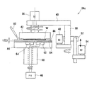
図2は、本発明の実施の形態の電解加工装置を備えた基板処理装置の構成を示す平面図である。図2に示すように、この基板処理装置は、例えば、図1(b)に示す、表面に導電性膜(被加工部)としての銅膜6及びバリア膜5を有する基板Wを収納したカセットを搬出入する搬出入部としての一対のロード・アンロード部30と、基板の1次洗浄を行う第1洗浄機31aと、基板の2次洗浄(仕上げ洗浄)を行う第2洗浄機31bと、基板Wを反転させる反転機32と、電解加工装置34とを備えている。これらの機器は、直列に配置されており、これらの機器の間で基板Wを搬送して授受する搬送装置としての搬送ロボット36がこれらの機器と平行に走行自在に配置されている。また、電解加工装置34を制御する制御部38がロード・アンロード部30に隣接して配置されている。
FIG. 2 is a plan view showing the configuration of the substrate processing apparatus including the electrolytic processing apparatus according to the embodiment of the present invention. As shown in FIG. 2, this substrate processing apparatus includes, for example, a cassette containing a substrate W having a
図3は、電解加工装置34を模式的に示す縦断面図である。図3に示すように、電解加工装置34は、上下動可能かつ水平方向に揺動自在なアーム40と、アーム40の自由端に垂設され、表面を下向き(フェースダウン)して基板Wを着脱自在に保持する基板保持部42と、基板保持部42の下方に配置される円板状で絶縁体からなる電極部44と、電極部44の加工電極62及び給電電極64に接続される電源46を備えている。
FIG. 3 is a longitudinal sectional view schematically showing the
アーム40は、揺動用モータ48に連結された揺動軸50の上端に取付けられており、揺動用モータ48の駆動に伴って水平方向に揺動する。また、この揺動軸50は、上下方向に延びるボールねじ52に連結されており、ボールねじ52に連結された上下動用モータ54の駆動に伴ってアーム40と共に上下動する。
The
基板保持部42は、基板保持部42で保持した基板Wと電極部44とを相対運動させる第1駆動部としての自転用モータ56に接続されており、この自転用モータ56の駆動に伴って回転(自転)する。また、上述したように、アーム40は、上下動及び水平方向に揺動可能となっており、基板保持部42は、アーム40と一体となって上下動及び水平方向に揺動する。電極部44は、基板Wと電極部44とを相対運動させる第2駆動部としての中空モータ60に接続されており、この中空モータ60の駆動に伴って、自転を行わない公転運動、いわゆるスクロール運動(並進回転運動)を行う。なお、中空モータ60の駆動に伴って、電極部44が、基板保持部42の回転中心から編心した位置を回転中心とした回転(自転)運動を行うようにしてもよいことは勿論である。
The
電極部44には、例えば扇状の複数の加工電極62と給電電極64が表面(上面)を露出させて交互に埋設されている。この例では、電極部44、加工電極62及び給電電極64が表面(上面)が面一となるようになっている。加工電極62は電源46の陰極に接続され、給電電極64は電源46の陽極に接続される。
In the
この実施の形態では、例えば、銅を加工する場合においては、陰極側に電解加工作用が生じるので、電源46の陰極に接続した電極が加工電極62となり、電源46の陽極に接続した電極が給電電極64となって、この加工電極62と給電電極64が円周方向に沿って交互に配置されるようになっている。加工材料によっては、電源46の陰極に接続される電極を給電電極とし、陽極に接続される電極を加工電極としてもよい。すなわち、被加工材料が、例えば銅、モリブデンまたは鉄である場合には、陰極側に電解加工作用が生じるため、電源46の陰極に接続した電極が加工電極62となり、陽極に接続した電極が給電電極64となる。一方、被加工材料が例えばアルミニウムやシリコンである場合には、陽極側で電解加工作用が生じるため、電源46の陽極に接続した電極が加工電極となり、陰極に接続した電極が給電電極となる。
In this embodiment, for example, when processing copper, an electrolytic processing action occurs on the cathode side, so that the electrode connected to the cathode of the
被加工部が錫酸化物やインジウム錫酸化物(ITO)などの導電性酸化物の場合には、被加工部を還元した後に、電解加工を行う。すなわち、図3において、電源46の陽極に接続した電極が還元電極となり、陰極に接続した電極が給電電極となるようにして、導電性酸化物の還元を行う。続いて、先程給電電極であった電極を加工電極として、還元された導電性酸化物の加工を行う。あるいは、導電性酸化物の還元時の極性を反転させることによって還元電極を加工電極にしてもよい。また被加工物を陰極にして、陽極電極を対向させることによっても導電性酸化物の除去加工ができる。
In the case where the processed part is a conductive oxide such as tin oxide or indium tin oxide (ITO), electrolytic processing is performed after the processed part is reduced. That is, in FIG. 3, the conductive oxide is reduced such that the electrode connected to the anode of the
なお、この例では、基板の表面に形成した導電性膜としての銅膜6やバリア膜5を電解加工するようにしているが、基板の表面に成膜乃至付着した不要なルテニウム(Ru)膜も同様にして、すなわちルテニウム膜を陽極となし、陰極に接続した電極を加工電極として、電解加工(エッチング除去)することができる。
In this example, the
このように、加工電極62と給電電極64とを円周方向に沿って交互に設けることで、基板Wの導電性膜(被加工部)に給電を行う給電部を設ける必要がなくなり、基板Wの全面の加工が可能となる。また、電圧、電流の印加方式としては、直流入力の他に、矩形波、パルス、サイン波入力でもよい。矩形波入力の場合、電圧、電流の入力は、正と負、正とゼロの矩形波であり、デュティ比は加工対象により任意で設定する。
Thus, by providing the
ここで、加工電極62及び給電電極64は、電解反応により、酸化または溶出が一般に問題となる。このため、電極の素材として、電極に広く使用されている金属や金属化合物よりも、炭素、比較的不活性な貴金属、導電性酸化物または導電性セラミックスを使用することが好ましい。この貴金属を素材とした電極としては、例えば、下地の電極素材にチタンを用い、その表面にめっきやコーティングで白金またはイリジウムを付着させ、高温で焼結して安定化と強度を保つ処理を行ったものが挙げられる。セラミックス製品は、一般に無機物質を原料として熱処理によって得られ、各種の非金属・金属の酸化物・炭化物・窒化物などを原料として、様々な特性を持つ製品が作られている。この中に導電性を持つセラミックスもある。電極が酸化すると電極の電気抵抗値が増加し、印加電圧の上昇を招くが、このように、白金などの酸化しにくい材料やイリジウムなどの導電性酸化物で電極表面を保護することで、電極素材の酸化による導電性の低下を防止することができる。
Here, oxidation or elution of the
電極部44の加工電極62及び給電電極64を囲む位置には、電極部44の内部に設けた液体流路44aに連通する液体供給孔44bが設けられ、液体流路44aは、ポンプ等の液体加圧部を有する液体供給源66から延び、中空モータ60の中空部の内部を貫通する液体供給管68に接続されている。これによって、液体供給源66から所定の圧力で供給される液体、好ましくは純水、更に好ましくは超純水を、液体供給管68及び液体流路44aを通過させ、液体供給孔44bから上方に向けて噴出して、液体を電極部44の上面の基板保持部42で保持した基板Wとの間に供給する液体供給部が構成されている。なお、本発明における加工液は、図示されるように複数の電極の間に設けられた供給孔から供給する場合や、電極自体に設けられた供給孔から供給する場合、電極部外から供給する場合などもある。
A
基板保持部42は、下方に開口した円筒状のハウジング70と、基板Wを吸着等で着脱自在に保持する円板状のチャッキングプレート72を有している。このチャッキングプレート72は、この下面に基板Wを保持した時、この基板Wの下面がハウジング70の下面がなす平面より下方に位置するようにハウジング70の内部に収納されている。そして、ハウジング70の下端には内方に突出する爪部70aが、チャッキングプレート72の上部には大径のフランジ部72aがそれぞれ設けられ、このフランジ部72aを爪部70aに係止させることで、チャッキングプレート72のハウジング70からの脱出が防止される。
The
チャッキングプレート72の上面周縁部には、一端をハウジング70の内周面に気密的に固着した円錐状のゴム等からなる弾性体74の他端が気密的に固着され、これによって、ハウジング70、チャッキングプレート72及び弾性体74で囲まれた空気室76が区画形成されている。ハウジング70の天井壁には、空気室76内に空気を導入する空気導入孔70bが設けられている。これによって、チャッキングプレート72は、空気室76内に導入された空気圧によって下方に押圧され、この状態で、チャッキングプレート72で保持した基板Wに基板Wを上方へ浮上させる浮上力が作用し、この浮上力がチャッキングプレート72を下方に押圧する押圧力より大きくなると、チャッキングプレート72のフランジ部72aがハウジング70の爪部70aを離されて、チャッキングプレート72はフローティングした状態となる。しかもこのチャッキングプレート72の浮上位置は、基板Wを上方へ浮上させる浮上力の大きさに応じて上下動する。
The other end of an
電極部44の内部に位置して、基板保持部42で保持した基板Wの表面(下面)と電極部44内に埋設した加工電極62及び給電電極64の表面(上面)との距離Sを検出する検出器80が設けられている。この検出器80としては、例えば基板Wの表面で反射するレーザ光を受光して基板Wとの距離を検出する光学式(反射式)の距離センサや、基板Wの表面(導電性膜)に渦電流を生じさせて基板Wとの距離を検出する渦電流式の距離センサが使用される。
A distance S between the surface (lower surface) of the substrate W held by the
なお、電解加工の際のエンドポイントを検出する、いわゆるエンドポイントセンサを備えている場合には、エンドポイントセンサに検出器80としての役割を併用させても良い。この場合、導電性膜等の膜厚と、基板保持部42で保持した基板Wの下面と加工電極62及び給電電極64の上面との距離Sとを単一のセンサ(エンドポイントセンサ)で同時に計測することができる。
In addition, when a so-called end point sensor for detecting an end point at the time of electrolytic processing is provided, the end point sensor may be used in combination with the role of the
この検出器80からの出力は制御部38に入力され、この制御部38からの出力は、液体供給源66に入力されて液体供給源66のポンプ等の液体加圧部がフィードバック制御される。この例では、電解加工中に、液体供給源66から電極部44と基板保持部42で保持した基板Wとの間に供給される液体の圧力を調整することで、加工電極62及び給電電極64の上面と基板保持部42で保持した基板Wとの距離Sが、互いに非接触で100μm以下の所定値となるようにしている。この距離Sは、50μm以下であることが好ましく、10μm以下、更には1μm以下であることがより好ましい。
The output from the
つまり、電極部44と基板保持部42のチャッキングプレート72で保持した基板Wとの間に所定の圧力の液体を供給しつつ電解加工を行いながら、基板Wの下面と加工電極62及び給電電極64の上面との距離Sを検出器80で検出する。そして、この距離Sが、例えば1μm以下の所定値より小さい場合には、液体供給源66から供給される液体の圧力を増大させてチャッキングプレート72のフローティング位置を上昇させ、大きいい場合には、液体供給源66から供給される液体の圧力を減少させてチャッキングプレート72のフローティング位置を下降させる。これによって、電解加工中、基板Wの下面と加工電極62及び給電電極64の上面との距離Sが、常に、例えば1μm以下の所定値となるようにする。
That is, the lower surface of the substrate W, the
次に、この基板処理装置を用いた基板処理(電解加工)について説明する。まず、例えば、図1(b)に示すように、表面に導電性膜(被加工部)として銅膜6及びシード層7を形成した基板Wを収納したカセットをロード・アンロード部30にセットし、このカセットから1枚の基板Wを搬送ロボット36で取出す。搬送ロボット36は、取出した基板Wを必要に応じて反転機32に搬送し、基板Wの導電性膜(銅膜6)を形成した表面が下を向くように反転させる。
Next, substrate processing (electrolytic processing) using this substrate processing apparatus will be described. First, for example, as shown in FIG. 1B, a cassette containing a substrate W on which a
搬送ロボット36は、反転させた基板Wを受け取って電解加工装置34に搬送し、基板保持部42のチャッキングプレート72により保持させる。この時、基板保持部42の空気室76内に、所定の圧力の空気を導入して封入し、これによって、チャッキングプレート72を所定の圧力で下方に押圧する。この状態で、アーム40を移動させて基板Wを保持した基板保持部42を電極部44の直上方の加工位置まで移動させる。次に、上下動用モータ54を駆動して基板保持部42を下降させ、このチャッキングプレート72で保持した基板Wを加工電極62及び給電電極64の表面に接触乃至近接させる。
The
次に、液体供給源66から所定の圧力の液体を電極部44と基板Wとの間に供給し、この時に液体供給孔44bから基板Wに向けて噴出され基板Wに作用する液体の圧力でチャッキングプレート72をフローティングさせながら、基板Wと加工電極62及び給電電極64との距離Sを検出器80で検出し、この距離Sが、例えば1μm以下の所定値となるように、液体供給源66から供給される液体の圧力を調整する。
Next, a liquid having a predetermined pressure is supplied from the
基板Wと加工電極62及び給電電極64との距離Sを、例えば1μm以下の所定値とした状態で、必要に応じて、自転用モータ56を駆動して基板Wを回転させ、同時に中空モータ60を駆動して電極部44をスクロール運動させることで、基板保持部42で保持した基板Wと加工電極62及び給電電極64とを相対運動させ、同時に、電源46により加工電極62と給電電極64との間に所定の電圧を印加する。これによって、液体中の水分子の解離によって生じた水酸化物イオンまたは水素イオンによって、加工電極(陰極)62において、基板Wの表面の導電性膜(銅膜6)の電解加工を行う。電解加工中、基板Wの下面と加工電極62及び給電電極64の上面との距離Sを検出器80で検出し、この距離Sが、常に、例えば1μm以下の所定値となるように、液体供給源66から供給される液体の圧力を調整する。
In a state where the distance S between the substrate W and the
ここで、図4に示すように、基板保持部42で保持した基板Wを、加工電極62との距離Sが10μm以下、好ましくは、数μm〜数百nmオーダとなるまで、可能な限り加工電極62に接触させることなく近接させた状態で電解加工を行うことが、基板Wの表面の、銅膜6(図1(b)参照)等の導電性膜表面の段差を解消する上で好ましい。すなわち、例えば、図1(b)に示す、半導体ウエハ等の基板Wの表面に形成した導電性膜として銅膜6の表面には、図4に示すように、通常200nm程度の数百nmオーダの凹凸段差Tがある。このため、例えば銅膜6の表面と加工電極62との距離Sが、例えば1mm程度であると、凹凸段差Tに対して極端に大きくなり、電気抵抗は距離に比例するが、銅膜6の表面の凹部底部から加工電極62までの距離R1と、凸部頂端から加工電極62までの距離R2が実質的に同じになってしまい、銅膜6の凸部のみを優先的に除去することが困難となる。しかし、銅膜6の表面と加工電極62との距離Sが、例えば1μmの場合には、凹凸段差Tに対して小さくなり、銅膜6の凸部先端を優先的に加工し、加工量の増加に伴って残留段差をより小さくして、銅膜6の表面をより平坦に加工することができる。
Here, as shown in FIG. 4, the substrate W held by the
図5は、被加工物(基板)と電極(加工電極)との距離Sを、50μm、10μm、1μm及び1mmと変化させ、液体として超純水を使用して電解加工(研磨)を行った時の、残留段差と加工量の関係を示す。この図5から、被加工物(基板)と電極(加工電極)との距離Sが1mmの時は初期凹凸が殆ど解消されず、この距離Sを50μmとすることで、初期凹凸を解消する効果が現れ、この距離Sを1μmとすることで、理想直線に近づくことが判る。 In FIG. 5, the distance S between the workpiece (substrate) and the electrode (working electrode) was changed to 50 μm, 10 μm, 1 μm, and 1 mm, and electrolytic processing (polishing) was performed using ultrapure water as a liquid. The relationship between the residual level difference and the processing amount is shown. From FIG. 5, when the distance S between the workpiece (substrate) and the electrode (working electrode) is 1 mm, the initial unevenness is hardly eliminated. By setting the distance S to 50 μm, the initial unevenness is eliminated. When this distance S is set to 1 μm, it can be seen that it approaches an ideal straight line.
一般的に、銅配線を形成するために半導体ウエハ等の基板に成膜した銅膜表面の初期凹凸段差は、200nm前後であることが多いので、上記の考察及び実験から、銅膜6の表面と加工電極62の距離Sは、一般には100μm程度で、50μm以下であることが好ましく、10μm以下、更には1μm以下であることがより好ましい。
In general, the initial unevenness step on the surface of a copper film formed on a substrate such as a semiconductor wafer in order to form a copper wiring is often around 200 nm. From the above considerations and experiments, the surface of the
この時、加工電極62と給電電極64との間に印加する電圧、またはこの間を流れる電流を制御部38でモニタして、エンドポイント(加工終点)を検知する。つまり、同じ電圧(電流)を印加した状態で電解加工を行うと、材料によって流れる電流(印加される電圧)に違いが生じる。例えば、図6(a)に示すように、表面に材料Bと材料Aとを順次成膜した基板Wの該表面に電解加工を施した時に流れる電流をモニタすると、材料Aを電解加工している間は一定の電流が流れるが、異なる材料Bの加工に移行する時点で流れる電流が変化する。同様に、加工電極62と給電電極64との間に印加される電圧にあっても、図6(b)に示すように、材料Aを電解加工している間は一定の電圧が印加されるが、異なる材料Bの加工に移行する時点で印加される電圧が変化する。なお、図6(a)は、材料Bを電解加工する時の方が、材料Aを電解加工する時よりも電流が流れにくくなる場合を、図6(b)は、材料Bを電解加工する時の方が、材料Aを電解加工するときよりも電圧が高くなる場合の例を示している。これにより、この電流または電圧の変化をモニタすることでエンドポイントを確実に検知することができる。
At this time, the voltage applied between the machining
なお、この例では、制御部38で加工電極62と給電電極64との間に印加する電圧、またはこの間を流れる電流をモニタして加工終点を検知するようにした例を示しているが、この制御部38で、加工中の基板の状態の変化をモニタして、任意に設定した加工終点を検知するようにしてもよい。この場合、加工終点は、被加工面の指定した部位について、所望の加工量に達した時点、若しくは加工量と相関関係を有するパラメータついて、所望の加工量に相当する量に達した時点を指す。このように、加工の途中においても、加工終点を任意に設定して検知できるようにすることで、多段プロセスでの電解加工が可能となる。
In this example, the
例えば、基板が異材料に達したときに生じる摩擦係数の違いによる摩擦力の変化や、基板の表面の凹凸を平坦化する際、凹凸を除去したことにより生じる摩擦力の変化等を検出することで加工量を判断し、加工終点を検出することとしてもよい。また、被加工面の電気抵抗による発熱や、加工面と被加工面との間に液体(純水)の中を移動するイオンと水分子の衝突による発熱が生じ、例えば基板の表面に堆積した銅膜を定電圧制御で電解研磨する際には、電解加工が進み、バリア膜や絶縁膜が露出するのに伴って、電気抵抗が大きくなり電流値が小さくなって発熱量が順に減少する。したがって、この発熱量の変化を検出することで加工量を判断し、加工終点を検出することとしてもよい。あるいは、異材料に達した時に生じる反射率の違いによる反射光の強度の変化を検出して、基板上の被加工膜の膜厚を検知し、これにより加工終点を検出してもよい。 For example, detecting changes in frictional force due to differences in the coefficient of friction that occurs when the substrate reaches a different material, or changes in frictional force resulting from removing irregularities when flattening irregularities on the surface of the substrate It is also possible to determine the processing amount and detect the processing end point. In addition, heat generated due to electrical resistance of the work surface and heat generated by collision of ions and water molecules moving in the liquid (pure water) between the work surface and the work surface occurred, for example, deposited on the surface of the substrate. When electrolytic polishing of a copper film is performed with constant voltage control, as the electrolytic processing proceeds and the barrier film and insulating film are exposed, the electrical resistance increases, the current value decreases, and the amount of heat generation decreases sequentially. Therefore, the processing amount may be determined by detecting the change in the heat generation amount, and the processing end point may be detected. Alternatively, it is also possible to detect a change in the intensity of reflected light due to a difference in reflectance that occurs when a different material is reached, detect the film thickness of the film to be processed on the substrate, and thereby detect the processing end point.
また、銅膜等の導電性膜の内部に渦電流を発生させ、基板の内部を流れる渦電流をモニタし、例えば周波数やインピーダンスの変化を検出して、基板上の被加工膜の膜厚を検知し、これにより加工終点を検出してもよい。更に、電解加工にあっては、加工電極と給電電極との間を流れる電流値で加工レートが決まり、加工量は、この電流値と加工時間の積で求められる電気量に比例する。したがって、電流値と加工時間の積で求められる電気量を積算し、この積算値が所定の値に達したことを検出することで加工量を判断し、加工終点を検出してもよい。 In addition, an eddy current is generated inside a conductive film such as a copper film, and the eddy current flowing inside the substrate is monitored. For example, a change in frequency or impedance is detected, and the film thickness of the film to be processed on the substrate is determined. It may be detected to detect the processing end point. Further, in the electrolytic machining, the machining rate is determined by the current value flowing between the machining electrode and the feeding electrode, and the machining amount is proportional to the amount of electricity obtained by the product of the current value and the machining time. Therefore, the machining end point may be detected by integrating the amount of electricity obtained by the product of the current value and the machining time, determining that the accumulated value has reached a predetermined value, and determining the machining end point.
電解加工完了後、電源46と加工電極62及び給電電極64との接続を切り、基板保持部42と電極部44の回転を停止させ、更に、電極部44と基板Wとの間への液体の供給を停止する。しかる後、基板保持部42を上昇させ、アーム40を移動させて基板Wを搬送ロボット36に受渡す。基板Wを受け取った搬送ロボット36は、必要に応じて反転機32に搬送して反転させ、第1洗浄機31aに搬送して基板の1次洗浄を、第2洗浄機31bに搬送して基板の2次洗浄(仕上げ洗浄)を、順次行って乾燥させ、乾燥後の基板Wをロード・アンロード部30のカセットに戻す。
After the electrolytic processing is completed, the
ここで、電解加工中に基板Wと電極部44との間に供給する液体として、電気伝導度が大き過ぎるものを使用すると、距離比から生じる抵抗比は同じであるものの、抵抗値そのものが小さくなる。このため、距離の違いによる抵抗差は小さくなり、例えば凹凸を有する導電性膜の表面を、該凹凸を解消しつつ平坦に加工することが困難となる。このため、この液体として、純水または超純水を使用することが好ましい。純水は、例えば電気伝導度が10μS/cm以下の水であり、超純水は、例えば電気伝導度が0.1μS/cm以下の水である。このように電解質を含まない純水または超純水を使用して電解加工を行うことで、基板Wの表面に電解質等の余分な不純物が付着したり、残留したりすることをなくすことができる。しかも、液体として、電気伝導度が小さい純水または超純水を使用することで、距離の違いによる抵抗差を大きくして、例えば凹凸を有する導電性膜の表面を、該凹凸を解消しつつ平坦に加工することができる。
Here, if the liquid supplied between the substrate W and the
純水または超純水の代わりに、電気伝導度500μS/cm以下の液体、例えば純水または超純水に電解質を添加した電解液を使用してもよい。電解液を使用することで、電気抵抗を低減して消費電力を削減することができる。この電解液としては、例えば、NaClやNa2SO4等の中性塩、HClやH2SO4等の酸、更には、アンモニア等のアルカリなどの溶液を使用することができ、被加工物の特性によって適宜選択して使用することができる。 Instead of pure water or ultrapure water, a liquid having an electric conductivity of 500 μS / cm or less, for example, an electrolytic solution obtained by adding an electrolyte to pure water or ultrapure water may be used. By using the electrolytic solution, electric resistance can be reduced and power consumption can be reduced. As this electrolytic solution, for example, a neutral salt such as NaCl or Na 2 SO 4 , an acid such as HCl or H 2 SO 4 , or an alkali such as ammonia can be used. Depending on the characteristics, it can be appropriately selected and used.
更に、純水または超純水の代わりに、純水または超純水に界面活性剤等を添加して、電気伝導度が500μS/cm以下、好ましくは、50μS/cm以下、更に好ましくは、0.1μS/cm以下(比抵抗で10MΩ・cm以上)にした液体を使用してもよい。このように、純水または超純水に界面活性剤を添加することで、基板Wと加工電極62の界面にイオンの移動を防ぐ一様な抑制作用を有する層を形成し、これによって、イオン交換(金属の溶解)の集中を緩和して被加工面の平坦性を向上させることができる。ここで、界面活性剤濃度は、100ppm以下が好ましい。
Furthermore, instead of pure water or ultrapure water, a surfactant or the like is added to pure water or ultrapure water, and the electric conductivity is 500 μS / cm or less, preferably 50 μS / cm or less, more preferably 0. A liquid having a specific resistance of 10 MΩ · cm or less may be used. In this way, by adding a surfactant to pure water or ultrapure water, a layer having a uniform suppressing action for preventing the movement of ions is formed at the interface between the substrate W and the
図7は、本発明の他の実施の形態の電解加工装置34aを示す。図7に示す電解加工装置34aの図4に示す電解加工装置34と異なる点は、以下の通りである。すなわち、図7に示す電解加工装置34aは、液体供給部として、電極部44の上方に配置され、基板保持部42の側方から電極部44と基板保持部42で保持した基板Wとの間に液体を供給する液体供給ノズル82を備えたものを使用している。そして、検出器80から制御部38に入力された信号を自転用モータ56及び中空モータ60にフィードバックして自転用モータ56及び中空モータ60の回転速度を制御し、これによって、基板保持部42で保持した基板Wと電極部44に埋設した加工電極62及び給電電極64の相対運動速度を調整するようにしている。自転用モータ56及び中空モータ60の回転速度の一方のみを制御するようにしてもよい。
FIG. 7 shows an
この例は、電極部44と基板保持部42で保持した基板Wとの間の相対運動によって、この間に存在する液体に発生するハイドロプレーニング現象による液体力(動圧)を介して、つまり、電極部44と基板保持部42で保持した基板Wとの間の相対運動速度を変えることによって、電解加工の際に液体を介して基板Wに加えられる力の大きさを調整するようにしている。
In this example, the relative movement between the
つまり、電極部44と基板保持部42のチャッキングプレート72で保持した基板Wとの間に液体供給ノズル(液体供給部)82から液体を供給しつつ両者を相対運動させて電解加工を行いながら、基板Wの下面と加工電極62及び給電電極64の上面との距離Sを検出器80で検出する。そして、この距離Sが、例えば1μm以下の所定値より小さい場合には、電極部44と基板Wとの相対運動速度を増大させてチャッキングプレート72のフローティング位置を上昇させ、大きいい場合には、電極部44と基板Wとの相対運動速度を減少させてチャッキングプレート72のフローティング位置を下降させる。これによって、電解加工中、基板Wの下面と加工電極62及び給電電極64の上面との距離Sが、常に、例えば1μm以下の所定値となるようにする。
That is, while the liquid is supplied from the liquid supply nozzle (liquid supply unit) 82 between the
この例にあっては、前述と同様に、チャッキングプレート72で保持した基板Wを加工電極62及び給電電極64の表面に接触乃至近接させる。この時、電極部44と基板Wとの間への液体供給ノズル(液体供給部)82からの液体の供給を開始する。そして、自転用モータ56及び中空モータ60を回転させて電極部44と基板Wとを相対運動させ、この時に基板Wに作用する液体圧(動圧)でチャッキングプレート72をフローティングさせながら、基板Wと加工電極62及び給電電極64との距離Sを検出器80で検出し、この距離Sが、例えば1μm以下の所定値となるように、自転用モータ56及び中空モータ60の回転速度を調整する。
In this example, as described above, the substrate W held by the chucking
基板Wと加工電極62及び給電電極64との距離Sを、例えば1μm以下の所定値とした状態で、電源46により加工電極62と給電電極64との間に所定の電圧を印加する。これによって、液体中の水分子の解離によって生じた水酸化物イオンまたは水素イオンによって、加工電極(陰極)62において、基板Wの表面の導電性膜(銅膜6)の電解加工を行う。電解加工中、基板Wの下面と加工電極62及び給電電極64の上面との距離Sを検出器80で検出し、この距離Sが、常に、例えば1μm以下の所定値となるように、自転用モータ56及び中空モータ60の回転速度を調整する。
A predetermined voltage is applied between the processing
この基板Wと加工電極62及び給電電極64との相対運動速度は、一般的には0.1m/s以上で、1m/s以上であることが好ましく、2m/s以上であることが更に好ましい。
The relative motion speed between the substrate W and the
図8は、本発明の更に他の実施の形態の電解加工装置34bを示す。この図8に示す電解加工装置34bの図3に示す電解加工装置34と異なる点は、電極部44の表面に、加工電極62及び給電電極64の表面を一体に覆う膜状のイオン交換体84を取付け、電解加工中に、検出器80でイオン交換体84の表面(上面)と基板Wの表面(下面)との距離Sを検出して、このイオン交換体84と基板Wとの距離Sを調整するようにした点にある。このイオン交換体84の各液体供給孔44bに対応する位置には、各液体供給孔44bから噴出される液体の流れが基板Wに直接当たるように、貫通孔が設けられている。
FIG. 8 shows an
このように、基板Wと加工電極62及び給電電極64との間にイオン交換体84を位置させることで、加工速度を大幅に向上させることができる。つまり、液体として超純水を使用した超純水電気化学的加工は、超純水中の水酸化物イオンと被加工材料との化学的相互作用によるものである。しかし、超純水中に含まれる反応種である水酸化物イオン濃度は、常温・常圧状態で10−7mol/Lと微量であるため、除去加工反応以外の反応(酸化膜形成等)による除去加工効率の低下が考えられる。このため、除去加工反応を高効率で行うためには、水酸化物イオンを増加させる必要がある。そこで、水酸化物イオンを増加させる方法として、触媒材料により超純水の解離反応を促進させる方法があり、その有力な触媒材料としてイオン交換体が挙げられる。具体的には、イオン交換体中の官能基と水分子との相互作用により水分子の解離反応に関する活性化エネルギを低下させる。これによって、水の解離を促進させて、加工速度を向上させることができる。
Thus, by positioning the
ここで、イオン交換体84としては、通水性に優れたものを使用することがより好ましい。純水や超純水等をイオン交換体84内を通過するように流すことで、水の解離反応を促進させる官能基(強酸性陽イオン交換材料ではスルホン酸基)に十分な水を供給して水分子の解離量を増加させ、水酸化物イオン(もしくはOHラジカル)との反応により発生した加工生成物(ガスも含む)を水の流れにより除去して、加工効率を高めることができる。
Here, it is more preferable to use an
イオン交換体84は、例えば、アニオン交換基またはカチオン交換基を付与した不織布等で構成することができる。カチオン交換基部は、好ましくは強酸性カチオン交換基(スルホン酸基)を担持したものであるが、弱酸性カチオン交換基(カルボキシル基)を担持したものでもよい。また、アニオン交換基部は、好ましくは強塩基性アニオン交換基(4級アンモニウム基)を担持したものであるが、弱塩基性アニオン交換基(3級以下のアミノ基)を担持したものでもよい。
The
ここで、例えば強塩基アニオン交換基を付与した不織布は、繊維径20〜50μmで空隙率が約90%のポリオレフィン製の不織布に、γ線を照射した後グラフト重合を行ういわゆる放射線グラフト重合法により、グラフト鎖を導入し、次に導入したグラフト鎖をアミノ化して第4級アンモニウム基を導入して作製される。導入されるイオン交換基の容量は、導入するグラフト鎖の量により決定される。グラフト重合を行うためには、例えばアクリル酸、スチレン、メタクリル酸グリシジル、更にはスチレンスルホン酸ナトリウム、クロロメチルスチレン等のモノマーを用い、これらのモノマー濃度、反応温度及び反応時間を制御することで、重合するグラフト量を制御することができる。したがって、グラフト重合前の素材の重量に対し、グラフト重合後の重量の比をグラフト率と呼ぶが、このグラフト率は、最大で500%が可能であり、グラフト重合後に導入されるイオン交換基は、最大で5meq/gが可能である。 Here, for example, a nonwoven fabric provided with a strong base anion exchange group is produced by a so-called radiation graft polymerization method in which a polyolefin nonwoven fabric having a fiber diameter of 20 to 50 μm and a porosity of about 90% is irradiated with γ rays and then graft polymerization is performed. The graft chain is introduced, and then the introduced graft chain is aminated to introduce a quaternary ammonium group. The capacity of the ion exchange group to be introduced is determined by the amount of graft chains to be introduced. In order to perform the graft polymerization, for example, using monomers such as acrylic acid, styrene, glycidyl methacrylate, sodium styrenesulfonate, chloromethylstyrene, and the like, by controlling the monomer concentration, reaction temperature, and reaction time, The amount of grafting to be polymerized can be controlled. Therefore, the ratio of the weight after graft polymerization to the weight of the material before graft polymerization is called the graft ratio. This graft ratio can be up to 500%, and the ion exchange groups introduced after the graft polymerization are A maximum of 5 meq / g is possible.
強酸性カチオン交換基を付与した不織布は、上記強塩基性アニオン交換基を付与する方法と同様に、繊維径20〜50μmで空隙率が約90%のポリオレフィン製の不織布に、γ線を照射した後グラフト重合を行ういわゆる放射線グラフト重合法により、グラフト鎖を導入し、次に導入したグラフト鎖を、例えば加熱した硫酸で処理してスルホン酸基を導入して作製される。また、加熱したリン酸で処理すればリン酸基が導入できる。ここでグラフト率は、最大で500%が可能であり、グラフト重合後に導入されるイオン交換基は、最大で5meq/gが可能である。 The nonwoven fabric provided with the strongly acidic cation exchange group was irradiated with γ-rays on a polyolefin nonwoven fabric having a fiber diameter of 20 to 50 μm and a porosity of about 90% in the same manner as the method of providing the strongly basic anion exchange group. The graft chain is introduced by a so-called radiation graft polymerization method in which post-graft polymerization is performed, and then the introduced graft chain is treated with, for example, heated sulfuric acid to introduce a sulfonic acid group. Moreover, a phosphoric acid group can be introduce | transduced if it processes with the heated phosphoric acid. Here, the graft ratio can be 500% at the maximum, and the ion exchange group introduced after the graft polymerization can be 5 meq / g at the maximum.
なお、イオン交換体84の素材の材質としては、ポリエチレン、ポリプロピレン等のポリオレフィン系高分子、またはその他、ポリウレタン等の有機高分子が挙げられる。また素材形態としては、不織布の他に、織布、シート、多孔質材、短繊維等が挙げられる。ここで、ポリエチレンやポリプロピレンは、放射線(γ線と電子線)を先に素材に照射する(前照射)ことで、素材にラジカルを発生させ、次にモノマーと反応させてグラフト重合することができる。これにより、均一性が高く、不純物が少ないグラフト鎖ができる。一方、その他の有機高分子は、モノマーを含浸させ、そこに放射線(γ線、電子線、紫外線)を照射(同時照射)することで、ラジカル重合することができる。この場合、均一性に欠けるが、ほとんどの素材に適用できる。
Examples of the material of the
このように、イオン交換体84をアニオン交換基またはカチオン交換基を付与した不織布で構成することで、純水または超純水や電解液等の液体が不織布の内部を自由に移動して、不織布内部の水分解触媒作用を有する活性点に容易に到達することが可能となって、多くの水分子が水素イオンと水酸化物イオンに解離される。更に、解離によって生成した水酸化物イオンが純水または超純水や電解液等の液体の移動に伴って効率良く運ばれるため、低い印加電圧でも高電流が得られる。
As described above, the
ここで、イオン交換体84をアニオン交換基またはカチオン交換基の一方を付与したもののみで構成すると、電解加工できる被加工材料が制限されるばかりでなく、極性により不純物が生成しやすくなる。そこで、アニオン交換基を有するアニオン交換体とカチオン交換基を有するカチオン交換体とを重ね合わせたり、イオン交換基部自体にアニオン交換基とカチオン交換基の双方の交換基を付与するようにしたりしてもよく、これにより、被加工材料の範囲を拡げるとともに、不純物を生成しにくくすることができる。
Here, when the
この例にあっては、電解加工中に、液体供給源66から電極部44と基板保持部42で保持した基板Wとの間に供給される液体の圧力を調整することで、イオン交換体84の上面と基板保持部42で保持した基板Wとの距離Sが、互いに非接触で100μm以下の所定値となるようにする。この距離Sは、50μm以下であることが好ましく、10μm以下、更には1μm以下であることがより好ましい。
In this example, the
これにより、例えば半導体ウエハ等の基板の表面に形成された導電性膜の表面に、例えば段差が200nm程度の凹凸があっても、この凹凸段差の凹部と凸部で電気抵抗差、ひいては加工速度差を生じさせて凹凸を平坦化し、しかもイオン交換体84と基板Wの表面とを互いに摺動させることなく電解加工を行うことで、基板Wの表面に欠陥が発生したり、イオン交換体84が磨耗したりするのを防止することができる。
As a result, even if the surface of the conductive film formed on the surface of a substrate such as a semiconductor wafer has unevenness with a level difference of about 200 nm, for example, there is a difference in electrical resistance between the concave and convex portions of the unevenness level and thus the processing speed. By producing a difference to flatten the unevenness and performing electrolytic processing without sliding the
図9は、本発明の他の実施の形態の電解加工装置34cを示す。この図9に示す電解加工装置34cの図7に示す電解加工装置34aと異なる点は、電極部44の表面に、加工電極62及び給電電極64の表面を一体に覆う膜状のイオン交換体84を取付け、電解加工中に、検出器80でイオン交換体84の表面(上面)と基板Wの表面(下面)との距離Sを検出して、このイオン交換体84と基板Wとの距離Sを調整するようにした点にある。
FIG. 9 shows an
つまり、この例にあっては、電解加工中に、自転用モータ56及び中空モータ60の少なくとも一方の回転速度を調整し、基板保持部42で保持した基板Wと電極部44に埋設した加工電極62及び給電電極64との相対運速度を調整することで、イオン交換体84の上面と基板保持部42で保持した基板Wとの距離Sが、互いに非接触で100μm以下の所定値となるようにする。この距離Sは、50μm以下であることが好ましく、10μm以下、更には1μm以下であることがより好ましい。
In other words, in this example, during the electrolytic processing, the rotational speed of at least one of the
図8及び図9に示す例のように、基板Wと加工電極62及び給電電極64との間にイオン交換体84を配置して電解加工を行うと、基板Wとイオン交換体84との間に吸着力が作用し、この吸着力は、加工電極62と給電電極64との間に印加する電圧に影響を受ける。このため、液体供給源66から電極部44と基板保持部42で保持した基板Wとの間に供給される液体の圧力を調整したり、基板保持部42で保持した基板Wと電極部44に埋設した加工電極62及び給電電極64との相対運速度を調整したりすることに代えて、またはこれらと併用して、加工電極62と給電電極64との間に印加する電圧を制御することで、イオン交換体84の上面と基板保持部42で保持した基板Wとの距離Sが、互いに非接触で100μm以下の所定値となるようにしてもよい。この距離Sは、50μm以下であることが好ましく、10μm以下、更には1μm以下であることがより好ましい。
被加工物とイオン交換体との距離を制御することができる。
When the
The distance between the workpiece and the ion exchanger can be controlled.
上記の各例にあっては、基板Wと加工電極62及び給電電極64との距離S、または基板Wと加工電極62及び給電電極64の表面を覆うイオン交換体84との距離Sを検出器80で検出するようにしているが、事前に校正曲線を作っておくことにより、検出器を不要となすようにしてもよい。この場合、基板と加工電極及び給電電極との距離、または基板とイオン交換体との距離は、基板に作用する液体圧または相対運動によって液体に発生する動圧から、基板の自重及び基板保持部の自重を差し引き、必要に応じて、基板Wとイオン交換体との間に作用する吸着力を更に差し引くことによって求められる。
In each of the above examples, the distance S between the substrate W and the
図10は、本発明の更に他の実施の形態の電解加工装置34dを示す。この実施の形態の電解加工装置34dの図7に示す電解加工装置34aと異なる点は、基板保持部42として、チャッキングプレート等を使用することなく、その下面で基板Wを直接的に吸着等で保持するようにしたものを使用し、更に、電極部44の表面に、加工電極62及び給電電極64を一体に覆う、厚さtが100μm以下の絶縁スペーサ86を取付けることによって、自転用モータ56や中空モータ60の回転速度の制御等を行わないようにした点にある。この絶縁スペーサ86の厚さtは、50μm以下であることが好ましく、10μm以下、更には1μm以下であることがより好ましい。
FIG. 10 shows an
この例にあっては、基板保持部42で保持した基板Wの表面(下面)を絶縁スペーサ86の表面(上面)に常に接触させた状態で、電極部44と基板Wとの間に液体を供給しつつ、自転用モータ56及び中空モータ60を駆動して基板Wと加工電極62及び給電電極とを相対運動させ、更に加工電極62と給電電極64との間に電圧を印加して電解加工を行う。これにより、基板Wと加工電極62及び給電電極64との距離Sが、自転用モータ56や中空モータ60の回転速度の制御等を行うことなく、常に絶縁スペーサ86の厚さtと等しく(t=S)、100μm以下、好ましくは50μm以下、更に好ましくは10μm以下、更には1μm以下となる。
In this example, in a state where the surface (lower surface) of the substrate W held by the
このように、基板Wと加工電極62及び給電電極64との距離Sを100μm以下、好ましくは50μm以下、更には好ましくは10μm以下、更には1μm以下とすることで、例えば半導体ウエハ等の基板に設けた凹凸を有する導電性膜の表面を、該凹凸を解消しつつ平坦に加工することができる。
Thus, by setting the distance S between the substrate W and the
絶縁スペーサ86は、多孔質材料からなることが好ましく、これにより、絶縁スペーサ86の通水性を確保して、超純水や純水等の液体が絶縁スペーサ86の内部を流通するようにすることができる。
The insulating
図11は、本発明の更に他の実施の形態の電解加工装置34eを示す。この実施の形態の電解加工装置34eの図10に示す電解加工装置34dと異なる点は、電極部44の表面に、加工電極62及び給電電極64を一体に覆うイオン交換体84を取付け、このイオン交換体84の表面(上面)に絶縁スペーサ86を取付けた点にある。
FIG. 11 shows an
この例にあっては、基板保持部42で保持した基板Wの表面(下面)を絶縁スペーサ86の表面(上面)に常に接触させた状態で、電極部44と基板Wとの間に液体を供給しつつ、自転用モータ56及び中空モータ60を駆動して基板Wと加工電極62及び給電電極とを相対運動させ、更に加工電極62と給電電極64との間に電圧を印加して電解加工を行う。これにより、基板Wとイオン交換体84との距離Sが、自転用モータ56や中空モータ60の回転速度の制御等を行うことなく、常に絶縁スペーサ86の厚さtと等しく(t=S)、100μm以下、好ましくは50μm以下、更に好ましくは10μm以下、更には1μm以下となる。
In this example, in a state where the surface (lower surface) of the substrate W held by the
このように、基板Wとイオン交換体84との距離Sを100μm以下、好ましくは50μm以下、更には好ましくは10μm以下、更には1μm以下とすることで、例えば半導体ウエハ等の基板に設けた凹凸を有する導電性膜の表面を、該凹凸を解消しつつ平坦に加工し、しかも、しかもイオン交換体84と基板Wの表面とを互いに摺動させることなく電解加工を行うことで、基板Wの表面に欠陥が発生したり、イオン交換体84が磨耗したりするのを防止することができる。
Thus, by setting the distance S between the substrate W and the
なお、上記各実施の形態では、基板保持部42を回転させ、同時に電極部44をスクロール運動させることで、基板Wと加工電極62及び給電電極64とを相対運動させて加工を行うようにしているが、基板Wと電極部44との相対運動はこの限りではなく、少なくとも一方が回転、偏心回転、並進、往復、スクロール運動するようにしてもよい。
In each of the above embodiments, the
また、電極部44に加工電極62と給電電極64とを埋設して、加工電極62と給電電極64が互いに相対移動しないようにした例を示しているが、加工電極と給電電極とを別体に構成して、両者が相対的に移動するようにしてもよい。この場合、加工電極と給電電極の少なくとも一方と基板との間に液体を供給しつつ、両者を相対運動させ、かつ両者の距離を100μm以下の所定値に制御して電解加工を行うようにしてもよい。また、加工電極と給電電極の少なくとも一方にイオン交換体を取付け、このイオン交換体を取付けた電極と基板との間に液体を供給しつつ、両者を相対運動させ、かつイオン交換体と基板との距離を100μm以下の所定値に制御して電解加工を行うようにしてもよい。
In addition, an example is shown in which the
30 ロード・アンロード部
31a,31b 洗浄機
32 反転機
34,34a,34b,34c,34d,34e 電解加工装置
36 搬送ロボット
38 制御部
40 アーム
42 基板保持部
44 電極部
44a 液体流路
44b 液体供給孔
46 電源
56 自転用モータ
60 中空モータ
62 加工電極
64 給電電極
66 液体供給源
68 液体供給管
70 ハウジング
72 チャッキングプレート
74 弾性体
76 空気室
80 検出器
82 液体供給ノズル
84 イオン交換体
86 絶縁スペーサ
30 load / unload
Claims (19)
前記被加工物に給電する給電電極と、
前記加工電極と前記給電電極との間に電圧を印加する電源と、
前記被加工物と前記加工電極または前記給電電極の少なくとも一方とを相対運動させる駆動部と、
前記被加工物と前記加工電極または前記給電電極の少なくとも一方との間に液体を供給する液体供給部と、
前記被加工物と前記加工電極または前記給電電極の少なくとも一方との距離を検出する検出器と、
前記検出器からの信号を基に前記被加工物と前記加工電極または前記給電電極の少なくとも一方との距離を100μm以下で互いに非接触な所定値に制御する制御部を有することを特徴とする電解加工装置。 A machining electrode that is freely accessible to the workpiece;
A feeding electrode for feeding power to the workpiece;
A power source for applying a voltage between the machining electrode and the power supply electrode;
A drive unit that relatively moves the workpiece and at least one of the processing electrode or the feeding electrode;
A liquid supply section for supplying a liquid between the workpiece and at least one of the processing electrode or the feeding electrode;
A detector for detecting a distance between the workpiece and at least one of the processing electrode or the feeding electrode;
An electrolysis system comprising: a control unit that controls a distance between the workpiece and at least one of the processing electrode and the power feeding electrode to a predetermined value that is 100 μm or less and non-contact based on a signal from the detector. Processing equipment.
前記被加工物に給電する給電電極と、
前記加工電極と前記給電電極との間に電圧を印加する電源と、
前記被加工物と前記加工電極または前記給電電極の少なくとも一方とを相対運動させる駆動部と、
前記被加工物と前記加工電極または前記給電電極の少なくとも一方との間に液体を供給する液体供給部と、
前記被加工物と前記加工電極または前記給電電極の少なくとも一方との間に配置されるイオン交換体と、
前記被加工物と前記イオン交換体との距離を検出する検出器と、
前記検出器からの信号を基に前記被加工物と前記イオン交換体との距離を100μm以下で互いに非接触な所定値に制御する制御部を有することを特徴とする電解加工装置。 A machining electrode that is freely accessible to the workpiece;
A feeding electrode for feeding power to the workpiece;
A power source for applying a voltage between the machining electrode and the power supply electrode;
A drive unit that relatively moves the workpiece and at least one of the processing electrode or the feeding electrode;
A liquid supply section for supplying a liquid between the workpiece and at least one of the processing electrode or the feeding electrode;
An ion exchanger disposed between the workpiece and at least one of the processing electrode or the feeding electrode;
A detector for detecting a distance between the workpiece and the ion exchanger;
An electrolytic processing apparatus comprising: a control unit configured to control a distance between the workpiece and the ion exchanger to a predetermined value that is 100 μm or less and non-contact based on a signal from the detector.
前記被加工物に給電する給電電極と、
前記加工電極と前記給電電極との間に電圧を印加する電源と、
前記被加工物と前記加工電極または前記給電電極の少なくとも一方とを相対運動させる駆動部と、
前記被加工物と前記加工電極または前記給電電極の少なくとも一方との間に液体を供給する液体供給部と、
前記被加工物と前記加工電極または前記給電電極の少なくとも一方との間に配置される厚さが100μm以下の絶縁スペーサを有することを特徴とする電解加工装置。 A machining electrode that is freely accessible to the workpiece;
A feeding electrode for feeding power to the workpiece;
A power source for applying a voltage between the machining electrode and the power supply electrode;
A drive unit that relatively moves the workpiece and at least one of the processing electrode or the feeding electrode;
A liquid supply section for supplying a liquid between the workpiece and at least one of the processing electrode or the feeding electrode;
An electrolytic processing apparatus comprising: an insulating spacer having a thickness of 100 μm or less disposed between the workpiece and at least one of the processing electrode or the feeding electrode.
前記被加工物に給電する給電電極と、
前記加工電極と前記給電電極との間に電圧を印加する電源と、
前記被加工物と前記加工電極または前記給電電極の少なくとも一方とを相対運動させる駆動部と、
前記被加工物と前記加工電極または前記給電電極の少なくとも一方との間に液体を供給する液体供給部と、
前記被加工物と前記加工電極または前記給電電極の少なくとも一方との間に配置されるイオン交換体と、
前記被加工物と前記イオン交換体との間に配置される厚さが100μm以下の絶縁スペーサを有することを特徴とする電解加工装置。 A machining electrode that is freely accessible to the workpiece;
A feeding electrode for feeding power to the workpiece;
A power source for applying a voltage between the machining electrode and the power supply electrode;
A drive unit that relatively moves the workpiece and at least one of the processing electrode or the feeding electrode;
A liquid supply section for supplying a liquid between the workpiece and at least one of the processing electrode or the feeding electrode;
An ion exchanger disposed between the workpiece and at least one of the processing electrode or the feeding electrode;
An electrolytic processing apparatus comprising an insulating spacer having a thickness of 100 μm or less disposed between the workpiece and the ion exchanger.
前記被加工物と前記加工電極または前記給電電極の少なくとも一方との距離を100μm以下で互いに非接触な所定値に保持しながら、前記被加工物と前記加工電極または前記給電電極の少なくとも一方を液体の存在下で相対運動させ、
前記加工電極と前記給電電極との間に電圧を印加することを特徴とする電解加工方法。 Prepare a machining electrode that is freely accessible to the workpiece and a feed electrode that feeds the workpiece,
While maintaining the distance between the workpiece and at least one of the processing electrode or the feeding electrode at a predetermined value which is 100 μm or less and non-contact with each other, at least one of the workpiece and the processing electrode or the feeding electrode is liquid Relative movement in the presence of
An electrolytic machining method, wherein a voltage is applied between the machining electrode and the feeding electrode.
前記被加工物と前記加工電極または前記給電電極の少なくとも一方との間にイオン交換体を配置し、
前記被加工物と前記イオン交換体との距離を100μm以下で互いに非接触な所定値に保持しながら、前記被加工物と前記加工電極または前記給電電極の少なくとも一方とを液体の存在下で相対運動させ、
前記加工電極と前記給電電極との間に電圧を印加することを特徴とする電解加工方法。 Prepare a machining electrode that is freely accessible to the workpiece and a feed electrode that feeds the workpiece,
An ion exchanger is disposed between the workpiece and at least one of the processing electrode or the feeding electrode,
While maintaining the distance between the workpiece and the ion exchanger at a predetermined value of 100 μm or less and non-contact with each other, the workpiece and at least one of the machining electrode and the feeding electrode are relatively positioned in the presence of a liquid. Exercise,
An electrolytic machining method, wherein a voltage is applied between the machining electrode and the feeding electrode.
前記被加工物と前記加工電極または前記給電電極の少なくとも一方との間に厚さが100μm以下の絶縁スペーサを配置し、
前記被加工物と前記加工電極または前記給電電極の少なくとも一方とを液体の存在下で前記絶縁スペーサに互いに接触させつつ相対運動させ、
前記加工電極と前記給電電極との間に電圧を印加することを特徴とする電解加工方法。 Prepare a machining electrode that is freely accessible to the workpiece and a feed electrode that feeds the workpiece,
An insulating spacer having a thickness of 100 μm or less is disposed between the workpiece and at least one of the processing electrode or the feeding electrode,
The workpiece and at least one of the processing electrode or the feeding electrode are moved relative to each other in contact with the insulating spacer in the presence of a liquid,
An electrolytic machining method, wherein a voltage is applied between the machining electrode and the feeding electrode.
前記被加工物と前記加工電極または前記給電電極の少なくとも一方との間にイオン交換体を配置し、
前記被加工物と前記イオン交換体との間に厚さが100μm以下の絶縁スペーサをイオン交換体に接触させて配置し、
前記被加工物と前記加工電極または前記給電電極の少なくとも一方を液体の存在下で前記絶縁スペーサと前記イオン交換体に互いに接触させつつ相対運動させ、
前記加工電極と前記給電電極との間に電圧を印加することを特徴とする電解加工方法。 Prepare a machining electrode that is freely accessible to the workpiece and a feed electrode that feeds the workpiece,
An ion exchanger is disposed between the workpiece and at least one of the processing electrode or the feeding electrode,
An insulating spacer having a thickness of 100 μm or less is disposed between the workpiece and the ion exchanger in contact with the ion exchanger,
Causing at least one of the workpiece and the processing electrode or the feeding electrode to move relative to each other while being in contact with the insulating spacer and the ion exchanger in the presence of a liquid;
An electrolytic machining method, wherein a voltage is applied between the machining electrode and the feeding electrode.
Priority Applications (2)
| Application Number | Priority Date | Filing Date | Title |
|---|---|---|---|
| JP2004318380A JP2006128576A (en) | 2004-11-01 | 2004-11-01 | Electrolytic processing apparatus and method therefor |
| US11/035,373 US7527723B2 (en) | 2004-01-16 | 2005-01-14 | Electrolytic processing apparatus and electrolytic processing method |
Applications Claiming Priority (1)
| Application Number | Priority Date | Filing Date | Title |
|---|---|---|---|
| JP2004318380A JP2006128576A (en) | 2004-11-01 | 2004-11-01 | Electrolytic processing apparatus and method therefor |
Publications (2)
| Publication Number | Publication Date |
|---|---|
| JP2006128576A true JP2006128576A (en) | 2006-05-18 |
| JP2006128576A5 JP2006128576A5 (en) | 2007-12-06 |
Family
ID=36722905
Family Applications (1)
| Application Number | Title | Priority Date | Filing Date |
|---|---|---|---|
| JP2004318380A Withdrawn JP2006128576A (en) | 2004-01-16 | 2004-11-01 | Electrolytic processing apparatus and method therefor |
Country Status (1)
| Country | Link |
|---|---|
| JP (1) | JP2006128576A (en) |
Cited By (1)
| Publication number | Priority date | Publication date | Assignee | Title |
|---|---|---|---|---|
| KR101164596B1 (en) | 2007-01-26 | 2012-07-11 | 삼성테크윈 주식회사 | Electrolyic etching device |
-
2004
- 2004-11-01 JP JP2004318380A patent/JP2006128576A/en not_active Withdrawn
Cited By (1)
| Publication number | Priority date | Publication date | Assignee | Title |
|---|---|---|---|---|
| KR101164596B1 (en) | 2007-01-26 | 2012-07-11 | 삼성테크윈 주식회사 | Electrolyic etching device |
Similar Documents
| Publication | Publication Date | Title |
|---|---|---|
| JP4043234B2 (en) | Electrolytic processing apparatus and substrate processing apparatus | |
| US7655118B2 (en) | Electrolytic processing apparatus and method | |
| US20070187257A1 (en) | Electrolytic processing apparatus and electrolytic processing method | |
| US7101465B2 (en) | Electrolytic processing device and substrate processing apparatus | |
| WO2004041467A1 (en) | Electrochemical machining device and electrochemical machining method | |
| US7527723B2 (en) | Electrolytic processing apparatus and electrolytic processing method | |
| JP2003205428A (en) | Electro-chemical machining apparatus, and method | |
| US20050051432A1 (en) | Electrolytic processing apparatus and method | |
| JP2008160134A (en) | Method for substrate treatment | |
| US20040256237A1 (en) | Electrolytic processing apparatus and method | |
| JP2008524434A (en) | Flattening method and flattening apparatus | |
| JP2007528933A (en) | Electrolytic processing apparatus and electrolytic processing method | |
| JP2006128576A (en) | Electrolytic processing apparatus and method therefor | |
| JP4233376B2 (en) | Substrate processing method | |
| JP4310085B2 (en) | Electrolytic machining method and apparatus | |
| JP4233331B2 (en) | Electrolytic machining method and apparatus | |
| US7563356B2 (en) | Composite processing apparatus and method | |
| JP2004002910A (en) | Electrolytic working method and apparatus | |
| JP2003175422A (en) | Electrochemical machining device and electrochemical machining method | |
| JP4127361B2 (en) | Electrolytic processing equipment | |
| JP2006013177A (en) | Apparatus and method for electrolytic processing | |
| JP2005264268A (en) | Electrochemical machining device and electrochemical machining method | |
| JP2007284795A (en) | Electrode structure and electrolytic processing device | |
| JP2005153142A (en) | Electrochemical machining apparatus | |
| JP2005054205A (en) | Electrochemical machining apparatus and electrochemical machining method |
Legal Events
| Date | Code | Title | Description |
|---|---|---|---|
| A521 | Written amendment |
Free format text: JAPANESE INTERMEDIATE CODE: A523 Effective date: 20071018 |
|
| A621 | Written request for application examination |
Free format text: JAPANESE INTERMEDIATE CODE: A621 Effective date: 20071018 |
|
| A761 | Written withdrawal of application |
Free format text: JAPANESE INTERMEDIATE CODE: A761 Effective date: 20090807 |