JP2006115413A - Imaging apparatus and imaging method - Google Patents
Imaging apparatus and imaging method Download PDFInfo
- Publication number
- JP2006115413A JP2006115413A JP2004303256A JP2004303256A JP2006115413A JP 2006115413 A JP2006115413 A JP 2006115413A JP 2004303256 A JP2004303256 A JP 2004303256A JP 2004303256 A JP2004303256 A JP 2004303256A JP 2006115413 A JP2006115413 A JP 2006115413A
- Authority
- JP
- Japan
- Prior art keywords
- signal
- frame rate
- timing
- solid
- clocks
- Prior art date
- Legal status (The legal status is an assumption and is not a legal conclusion. Google has not performed a legal analysis and makes no representation as to the accuracy of the status listed.)
- Pending
Links
- 238000003384 imaging method Methods 0.000 title claims abstract description 80
- 238000006243 chemical reaction Methods 0.000 claims abstract description 31
- 238000005070 sampling Methods 0.000 claims abstract description 19
- 238000000034 method Methods 0.000 claims description 10
- 230000010355 oscillation Effects 0.000 claims description 3
- 238000010586 diagram Methods 0.000 description 5
- 230000000875 corresponding effect Effects 0.000 description 3
- 230000000630 rising effect Effects 0.000 description 3
- 239000013078 crystal Substances 0.000 description 2
- 239000002131 composite material Substances 0.000 description 1
- 230000002596 correlated effect Effects 0.000 description 1
- 238000001514 detection method Methods 0.000 description 1
- 238000001914 filtration Methods 0.000 description 1
- 238000012986 modification Methods 0.000 description 1
- 230000004048 modification Effects 0.000 description 1
- 230000002093 peripheral effect Effects 0.000 description 1
- 230000010363 phase shift Effects 0.000 description 1
- 230000000750 progressive effect Effects 0.000 description 1
- 239000000758 substrate Substances 0.000 description 1
Images


Classifications
-
- H—ELECTRICITY
- H04—ELECTRIC COMMUNICATION TECHNIQUE
- H04N—PICTORIAL COMMUNICATION, e.g. TELEVISION
- H04N25/00—Circuitry of solid-state image sensors [SSIS]; Control thereof
Landscapes
- Engineering & Computer Science (AREA)
- Multimedia (AREA)
- Signal Processing (AREA)
- Transforming Light Signals Into Electric Signals (AREA)
- Studio Devices (AREA)
Abstract
Description
この発明は、CCD(Charge Coupled Device)等の固体撮像素子を用いた撮像装置に関し、特に、フレームレートを変換する撮像装置及び撮像方法に関する。 The present invention relates to an imaging apparatus using a solid-state imaging device such as a CCD (Charge Coupled Device), and more particularly to an imaging apparatus and an imaging method for converting a frame rate.
映像光を受け、これに応じた映像信号を出力する撮像装置として、例えば、CCD等の固体撮像素子を用いたものが知られている。このような撮像装置においては、複数種類の解像度で映像信号を出力することも可能となる。 2. Description of the Related Art As an imaging device that receives video light and outputs a video signal corresponding thereto, for example, a device using a solid-state imaging device such as a CCD is known. In such an imaging apparatus, it is also possible to output video signals with a plurality of types of resolutions.
特許文献1には、複数の解像度による映像信号を切り換えるCCD撮像装置が示されており、ユーザは、任意の解像度による映像信号を必要に応じて選択することができる。
しかし、特許文献1の従来技術においては、撮像装置のフレームレートを変更したい場合について、どのようにすればよいかを知ることができない。すなわち、一般に、CCD撮像装置においては、50fpsのフレームレートや60fpsのフレームレートが知られているが、例えば、フレームレート60fps用に設計された撮像装置は、フレームレート50fpsでの映像出力を得るようには、容易に変更することができないという問題がある。 However, in the prior art of Patent Document 1, it is impossible to know how to change the frame rate of the imaging apparatus. That is, generally, a CCD imaging device has a frame rate of 50 fps or a frame rate of 60 fps. For example, an imaging device designed for a frame rate of 60 fps can obtain a video output at a frame rate of 50 fps. Has a problem that it cannot be easily changed.
本発明は、CCD駆動周波数や、発振器、電気フィルタの部品や回路を変更することなく、容易にフレームレートを切り替えることが可能なCCD固体撮像素子を用いた撮像装置及び撮像方法を提供することを目的とする。 The present invention provides an image pickup apparatus and an image pickup method using a CCD solid-state image pickup device capable of easily switching the frame rate without changing the CCD drive frequency, oscillator, electric filter components and circuits. Objective.
映像光を受光しこれに応じた電荷信号を、与えられるタイミング信号に応じて出力する固体撮像素子と、前記固体撮像素子からの電荷信号を、与えられるタイミング信号に応じてサンプリングしサンプリング結果に応じたサンプル信号を出力するサンプリング部と、前記サンプリング部からのサンプル信号を、与えられるタイミング信号に応じてデジタル信号に変換するA/D変換部と、前記デジタル信号について、所定処理を施して出力するデジタル処理部と、前記所定処理を施したデジタル信号をアナログ信号に変換した映像信号を出力するD/A変換部と、第1フレームレート(60fps)の映像信号を前記D/A変換部から得る場合に供給する前記タイミング信号の水平期間の第1クロック数に対して、前記第1フレームレートよりも低い第2フレームレート(50fps)の映像信号を得る場合に、前記第1クロック数よりも高い水平期間のクロック数のタイミング信号を生成しこれに基づくタイミング信号を、前記固体撮像素子と前記サンプリング部と前記A/D変換部との内の少なくとも一つに供給するタイミング部とを具備することを特徴とする撮像装置である。 A solid-state image sensor that receives video light and outputs a charge signal corresponding to the received light signal according to a given timing signal, and a charge signal from the solid-state image sensor is sampled according to the given timing signal, and according to the sampling result A sampling unit that outputs the sample signal, an A / D conversion unit that converts the sample signal from the sampling unit into a digital signal in accordance with a given timing signal, and outputs the digital signal after performing predetermined processing A digital processing unit, a D / A conversion unit that outputs a video signal obtained by converting the digital signal subjected to the predetermined processing into an analog signal, and a video signal having a first frame rate (60 fps) are obtained from the D / A conversion unit. The first frame rate with respect to the first number of clocks in the horizontal period of the timing signal to be supplied. When a video signal having a lower second frame rate (50 fps) is obtained, a timing signal having a clock number of a horizontal period higher than the first clock number is generated, and a timing signal based on the timing signal is generated as the sampling signal and the sampling signal. And an A / D converter, and a timing unit for supplying to at least one of the A / D converters.
上述した撮像装置においては、フレームレートを変更する際に、CCD駆動周波数を変更することなく、水平期間のクロック数を高めることにより、フレームレートを変更するものである。 In the imaging apparatus described above, when changing the frame rate, the frame rate is changed by increasing the number of clocks in the horizontal period without changing the CCD drive frequency.
これにより、例えば、フレームレートを変更するべく、CCD駆動周波数を変更した場合と比較すると、発振器の周波数変更・電気フィルタの特性変更や、回路のトータル遅延量に対する高速パルス(CDS用S/Hパルス、A/Dクロック)の位相変更のリスク等がなくなる。従って、本発明によれば、容易な方法により、フレームレートを変更することができる、固体撮像素子等を用いた撮像装置を提供することができる。 Thus, for example, compared with the case where the CCD drive frequency is changed in order to change the frame rate, the oscillator frequency change, the electric filter characteristic change, and the high-speed pulse (CDS S / H pulse for the total delay amount of the circuit) , A / D clock) phase change risk and the like are eliminated. Therefore, according to the present invention, it is possible to provide an imaging apparatus using a solid-state imaging device or the like that can change the frame rate by an easy method.
以下、この発明の実施の形態について図面を参照して詳細に説明する。
本発明に係る撮像装置は、CCD素子等の固体撮像素子を用いる撮影装置である。図1は、本発明の一実施形態に係る撮像装置の構成の一例を示すブロック図、図2は、同じく撮像装置のCCD素子の構成の一例を示す平面図、図3は、同じく撮像装置において、フレームレート60fpsから50fpsへの変換をCCD駆動周波数を減少させることで行った場合を説明する説明図、図4は、同じく撮像装置において、フレームレート60fpsから50fpsへの変換をCCD駆動周波数を減少させることで行った場合を示すタイミングチャート、図5は、同じく撮像装置において、フレームレート60fpsから50fpsへの変換をCCD駆動周波数を減少させることで行った場合を示すタイミングチャート、図6は、同じく撮像装置において、フレームレート60fpsから50fpsへの変換を水平期間クロック数を増加させることで行った場合を示す説明図、図7は、同じく撮像装置において、フレームレート60fpsから50fpsへの変換を水平期間クロック数を増加させることで行った場合を示すタイミングチャート、図8は、同じく撮像装置において、フレームレート50fpsから60fpsへの変換を水平期間クロック数を減少させることで行った場合を示す説明図、図9は、同じく撮像装置において、フレームレート50fpsから60fpsへの変換を水平期間クロック数を減少させることで行った場合を示すタイミングチャートである。
Hereinafter, embodiments of the present invention will be described in detail with reference to the drawings.
The imaging apparatus according to the present invention is an imaging apparatus that uses a solid-state imaging element such as a CCD element. FIG. 1 is a block diagram showing an example of the configuration of an imaging apparatus according to an embodiment of the present invention, FIG. 2 is a plan view showing an example of the configuration of a CCD element of the imaging apparatus, and FIG. FIG. 4 is an explanatory diagram for explaining a case where the conversion from the frame rate 60 fps to 50 fps is performed by reducing the CCD drive frequency. FIG. FIG. 5 is a timing chart showing the case where the conversion from the frame rate of 60 fps to 50 fps is carried out by reducing the CCD drive frequency in the imaging apparatus, and FIG. In the imaging device, conversion from a frame rate of 60 fps to 50 fps is performed in the horizontal period. FIG. 7 is a timing chart showing a case where conversion from a frame rate of 60 fps to 50 fps is performed by increasing the number of clocks in the horizontal period in the image pickup apparatus. 8 is an explanatory diagram showing a case where the conversion from the frame rate of 50 fps to 60 fps is performed by reducing the number of horizontal period clocks in the imaging apparatus, and FIG. It is a timing chart which shows the case where conversion is performed by reducing the number of horizontal period clocks.
<本発明に係る撮像装置の構成>
本発明に係る撮像装置Mは、図1に示すように、固体撮像素子であるCCD11と、この出力である電荷信号を受けるアナログ回路であるCDS(Correlate Double Sample)回路(相関二重サンプリング回路)12と、この出力を高周波につきフィルタリングするフィルタ13と、フィルタの出力につき、色補正、ガンマ補正を行う信号処理部14と、この出力をA/D変換するA/D変換器15と、変換されたデジタル信号について、例えば、Gチャンネル画素の補正処理や、スケーリング処理、IP変換等を行うデジタル信号処理部16と、この出力をD/A変換するD/A変換器17とを有している。
<Configuration of Imaging Device According to the Present Invention>
As shown in FIG. 1, an imaging apparatus M according to the present invention includes a
ここで、撮像装置MのこのCCD11、CDS回路12、フィルタ13、信号処理部14、A/D変換器15、デジタル信号処理部16、D/A変換器17等は、撮像装置Mが、例えば、RGB毎の画像信号を出力するものであれば、Rチャネル、Gチャネル、Bチャネル毎に3系列が平行して構成されるものである。
Here, the
一方、撮像装置Mは、これらの構成とは異なり、クリスタル発振等による発振器20と、ここから発振クロックを受けて、所望のタイミング信号をCCD11、CDS12、A/D変換器15等に供給するタイミングジェネレータ18と、タイミングジェネレータ18にプログラムや設定値を供給するROM21と、タイミングジェネレータ18から、所望のタイミング信号を受けて、垂直駆動パルスをCCD11に供給するVドライバ19とを有している。
On the other hand, unlike these configurations, the imaging apparatus M receives an
又、固体撮像素子であるCCD素子11は、一例として、図2に示されるように、約1センチ四方程度の基板上に、縦方向768行、横方向1024列の素子が並んで設けられている。RGB信号の仕様であれば、このようなCCD素子11が3つ設けられている。
As an example, as shown in FIG. 2, the
本発明に係る撮像装置Mは、上記の構成において、以下のように映像信号を出力する。すなわち、一例として、Rチャネル、Gチャネル、Bチャネル毎に構成されたCCD素子11から、一例として、約500mV程度の電荷信号がCDS回路12に出力される。
In the above configuration, the imaging apparatus M according to the present invention outputs a video signal as follows. That is, as an example, a charge signal of about 500 mV is output to the
このとき、動作タイミングとして、クリスタルの発信器20からのクロックに基づき、
ROM21等から与えられた値に基づいて、タイミングジェネレータ18から、CCD駆動パルス(水平駆動パルス)としてのタイミング信号がCCD素子11に与えられ、CCD素子11上の各画素毎の出力タイミングを提供している。同時に、タイミングジェネレータ18からタイミング信号がVドライバ19に供給され、Vドライバ19からは、1ライン分の1024個の素子のCCD駆動パルスの後に、次のラインに移動するタイミングである垂直駆動パルスがCCD素子11に供給されている。これら二つのタイミング信号により、フレーム毎の検出信号がCDS回路12に供給される。
At this time, based on the clock from the
A timing signal as a CCD drive pulse (horizontal drive pulse) is given to the
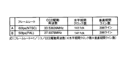
ここで、一例として、フレームレート60fpsの撮像装置Mの場合は、CCD駆動パルスのCCD駆動周波数は、33.53639MHzであり、水平期間クロック数は、1411ckであり、垂直期間ライン数は、396ラインである。 Here, as an example, in the case of the imaging apparatus M with a frame rate of 60 fps, the CCD drive frequency of the CCD drive pulse is 33.53639 MHz, the horizontal period clock number is 1411 ck, and the vertical period line number is 396 lines. It is.
次に、CDS回路12では、CCD素子11から与えられた電荷信号を、タイミングジェネレータ18からのタイミング信号であるサンプリングホールドパルスに応じて、サンプリングし、サンプリングされた電荷信号は、フィルタ13で高周波ノイズを除去され、信号処理部14に供給される。信号処理部14においては、高周波ノイズを除去された画像信号について、例えば、色補正処理、ガンマ補正処理が施される。
Next, the
更に、信号処理部14からの出力を、タイミングジェネレータ18からのタイミング信号であるA/Dクロック信号に応じて、A/D変換を行って、デジタル信号をデジタル信号処理部16に供給する。デジタル信号処理部16においては、デジタル信号について、スケーリング処理や、IP変換等をおこなう。
Further, the output from the
スケーリング処理とは、見かけ上の解像度を向上させるべく、先のCCD素子11において、Gチャネルにつき、RチャネルとBチャネルに対して半画素分だけずらして設定し、後に、デジタル信号syロイブ16等において、このずれ分を戻すべく処理を行うことで、2048画素分の信号とするものである。又、IP変換とは、インターレース画像信号をプログレッシブ画像信号に順番を変更する処理である。
In the scaling process, in order to improve the apparent resolution, the G channel is set so as to be shifted by a half pixel with respect to the R channel and the B channel in the
その後、このデジタル画像信号をD/A変換器17においてD/A変換し、コンポジットのビデオ出力信号等のアナログの色画像信号として出力する。
Thereafter, the digital image signal is D / A converted by the D /
<フレームレートの変更>
(CCD駆動周波数の変更による対応)
一般に、CCD素子等を利用した撮像装置においては、60fps(frame per second)又は50fpsのフレームレートを取ることが多い。ここで、例えば、図3に示すように、ケースAの撮像装置Mにおいては、フレームレート60の場合、CCD駆動周波数を33.53639MHz、水平期間クロック数1411ck、垂直期間ライン数396ラインにより、タイミングジェネレータ18の設定、及び、CDS回路12及びA/D変換器15等の回路定数が決められている。
<Change frame rate>
(Corresponding to change of CCD drive frequency)
In general, an imaging apparatus using a CCD element or the like often takes a frame rate of 60 fps (frame per second) or 50 fps. Here, for example, as shown in FIG. 3, in the imaging apparatus M of case A, when the frame rate is 60, the CCD drive frequency is 33.53639 MHz, the horizontal period clock number is 1411 ck, and the vertical period line number is 396 lines. Settings of the
これを、フレームレート60fpsから50fpsに変換して使用したい場合、一般的には図3及び図4のケースBに示すように、発振器20を交換し、CCD駆動周波数を27.9378MHzに変更し、これに応じて周辺回路の回路定数等も変更して対応する方法が考えられる。
When it is desired to use this by converting the frame rate from 60 fps to 50 fps, generally, as shown in case B of FIGS. 3 and 4, the
しかし、この方法をとると、発振器20、フィルタ13等の部品の変更が必要となる。更に、図5のBの場合における矢印に示すように、A/Dクロックの立ち上がりタイミングとCCD出力のタイミングとが最適な値にて合致しなくなる(位相ずれ)。すなわち、A/Dクロックの立ち上がりタイミングは、『Aの場合』のように、CCD出力の各センターに合致することが安定した信号を検出するために必要である。しかし、『Bの場合』では、A/Dクロックの立ち上がりタイミングは、CCD出力の各センターからはずれたタイミングとなっており、これでは、CCD出力の値が後段に正確に伝わらないという不具合がある。
However, when this method is adopted, it is necessary to change components such as the
(水平期間クロック数の変更による対応:60→50)
次に、タイミングジェネレータ18において、図6に示すように、水平期間クロック数を変更することによりフレームレートを変更する方法を示す。すなわち、ケースAのフレームレート60fpsに対して、ケースCのフレームレート50fpsとするとき、CCD駆動周波数は、33.53639MHzのままで変更することなく、水平期間クロック数を1694ckに変更することにより、フレームレートの変更を実現するものである。
(Response by changing the number of horizontal period clocks: 60 → 50)
Next, in the
これは、図6に示す式1で明らかである。すなわち、フレームレートは、
(フレームレート)
=1/((1/CCD駆動周波数)×(水平期間クロック数)×(垂直期間ライン数))
により定義される値である。
This is apparent from Equation 1 shown in FIG. That is, the frame rate is
(frame rate)
= 1 / ((1 / CCD driving frequency) × (number of horizontal period clocks) × (number of vertical period lines))
Is a value defined by
ここで、タイミングジェネレータ18をPLDで構成することで、PLDのROM21の内容を書き換えることにより、水平駆動停止期間を変更することができるので、回路の変更は不要となる。
Here, by configuring the
このような方法により、発振器、電気フィルタ、高速パルス(CDS用S/Hパルス、A/Dクロック)位相等、信号処理回路を変更することなくフレームレートを変換することが可能となる。 By such a method, it becomes possible to convert the frame rate without changing the signal processing circuit such as an oscillator, an electric filter, a high-speed pulse (CDS S / H pulse, A / D clock) phase, and the like.
(水平期間クロック数の変更による対応:50→60)
又、更に、フレームレートを大きくする場合も、水平期間クロック数を変更することにより可能となる。すなわち、図8の説明図が示すように、ケースDのフレームレート50fpsに対して、ケースEのフレームレート60fpsへの変更が可能である。この際に、CCD駆動周波数は、27.9378MHzから変更することなく、式1に基づいて、水平期間クロック数を1411ckから1178ckへと変更することで可能となる。この時、図9に示すように、水平駆動停止期間は、「305」から「70」となり、式1を満たすものである。
(Response by changing the number of horizontal period clocks: 50 → 60)
Further, the frame rate can be increased by changing the number of horizontal period clocks. That is, as illustrated in the explanatory diagram of FIG. 8, the frame rate of case D can be changed to the frame rate of 60 fps with respect to the frame rate of 50 fps. At this time, the CCD drive frequency can be changed by changing the number of horizontal period clocks from 1411 ck to 1178 ck based on Equation 1 without changing from 27.9378 MHz. At this time, as shown in FIG. 9, the horizontal drive stop period changes from “305” to “70”, which satisfies Expression 1.
これにより、撮像装置Mにおいて、ROM21等の定数等を変更するだけで、フレームレート50をフレームレート60に上げることが可能となり、発振器20の変更や、フィルタ13の変更等の作業も不要となるものである。
As a result, in the imaging apparatus M, it is possible to increase the frame rate 50 to the frame rate 60 only by changing constants of the
又、ここでは、フレームレート50fpsと60fpsとの場合を代表に説明したが、他の値のフレームレートの場合でも、同様の趣旨で容易なフレームレートの変更が可能となるものである。 Also, here, the case of frame rates of 50 fps and 60 fps has been described as a representative, but even in the case of other frame rates, it is possible to easily change the frame rate for the same purpose.
以上記載した様々な実施形態により、当業者は本発明を実現することができるが、更にこれらの実施形態の様々な変形例を思いつくことが当業者によって容易であり、発明的な能力をもたなくとも様々な実施形態へと適用することが可能である。従って、本発明は、開示された原理と新規な特徴に矛盾しない広範な範囲に及ぶものであり、上述した実施形態に限定されるものではない。 With the various embodiments described above, those skilled in the art can realize the present invention. However, it is easy for those skilled in the art to come up with various modifications of these embodiments, and have the inventive ability. It is possible to apply to various embodiments at least. Therefore, the present invention covers a wide range consistent with the disclosed principle and novel features, and is not limited to the above-described embodiments.
11…CCD、12…CSD、13…フィルタ、14…信号処理部、15…A/D変換部、16…デジタル信号処理部、17…D/A変換部、18…タイミングジェネレータ、19…Vドライバ、20…発振器、21…ROM。
DESCRIPTION OF
Claims (16)
前記固体撮像素子からの電荷信号を、与えられるタイミング信号に応じてサンプリングしサンプリング結果に応じたサンプル信号を出力するサンプリング部と、
前記サンプリング部からのサンプル信号を、与えられるタイミング信号に応じてデジタル信号に変換するA/D変換部と、
前記デジタル信号について、所定処理を施して出力するデジタル処理部と、
前記所定処理を施したデジタル信号をアナログ信号に変換した映像信号を出力するD/A変換部と、
第1フレームレートの映像信号を前記D/A変換部から得る場合に供給する前記タイミング信号の水平期間の第1クロック数に対して、前記第1フレームレートよりも低い第2フレームレートの映像信号を得る場合に、前記第1クロック数よりも水平期間のクロック数のタイミング信号を生成しこれに基づくタイミング信号を、前記固体撮像素子と前記サンプリング部と前記A/D変換部との内の少なくとも一つに供給するタイミング部と、
を具備することを特徴とする撮像装置。 A solid-state imaging device that receives video light and outputs a charge signal according to the received light according to a given timing signal;
A sampling unit that samples a charge signal from the solid-state imaging device according to a given timing signal and outputs a sample signal according to a sampling result;
An A / D converter that converts the sample signal from the sampling unit into a digital signal according to a given timing signal;
A digital processing unit that performs predetermined processing and outputs the digital signal;
A D / A converter for outputting a video signal obtained by converting the digital signal subjected to the predetermined processing into an analog signal;
A video signal having a second frame rate lower than the first frame rate with respect to a first clock number in a horizontal period of the timing signal supplied when a video signal having a first frame rate is obtained from the D / A converter. When generating a timing signal having a number of clocks in a horizontal period from the first clock number, a timing signal based on the timing signal is transmitted to at least one of the solid-state imaging device, the sampling unit, and the A / D conversion unit. A timing unit to supply to one,
An imaging apparatus comprising:
第1フレームレートの映像信号を前記D/A変換部から得る場合に供給する前記タイミング信号の水平期間の第1クロック数に対して、前記第1フレームレートよりも低い第2フレームレートの映像信号を得る場合に、前記第1クロック数よりも高いクロック数のタイミング信号を生成ししこれに基づくタイミング信号を、前記固体撮像素子と前記サンプリング部と前記A/D変換部との内の少なくとも一つに供給することで撮像を行う撮像方法。 A solid-state image sensor that receives video light and outputs a charge signal corresponding to the received light signal according to a given timing signal, and a charge signal from the solid-state image sensor is sampled according to the given timing signal, and according to the sampling result A sampling unit that outputs the sample signal, an A / D conversion unit that converts the sample signal from the sampling unit into a digital signal in accordance with a given timing signal, and outputs the digital signal after performing predetermined processing Using an imaging device having a digital processing unit,
A video signal having a second frame rate lower than the first frame rate with respect to a first clock number in a horizontal period of the timing signal supplied when a video signal having a first frame rate is obtained from the D / A converter. In the case of obtaining the timing signal, a timing signal having a clock number higher than the first clock number is generated, and a timing signal based on the timing signal is transmitted to at least one of the solid-state imaging device, the sampling unit, and the A / D conversion unit. An imaging method for performing imaging by supplying to one.
Priority Applications (2)
| Application Number | Priority Date | Filing Date | Title |
|---|---|---|---|
| JP2004303256A JP2006115413A (en) | 2004-10-18 | 2004-10-18 | Imaging apparatus and imaging method |
| US11/251,913 US7548265B2 (en) | 2004-10-18 | 2005-10-18 | Image pickup apparatus and image pickup method including clocks |
Applications Claiming Priority (1)
| Application Number | Priority Date | Filing Date | Title |
|---|---|---|---|
| JP2004303256A JP2006115413A (en) | 2004-10-18 | 2004-10-18 | Imaging apparatus and imaging method |
Publications (2)
| Publication Number | Publication Date |
|---|---|
| JP2006115413A true JP2006115413A (en) | 2006-04-27 |
| JP2006115413A5 JP2006115413A5 (en) | 2009-02-05 |
Family
ID=36205816
Family Applications (1)
| Application Number | Title | Priority Date | Filing Date |
|---|---|---|---|
| JP2004303256A Pending JP2006115413A (en) | 2004-10-18 | 2004-10-18 | Imaging apparatus and imaging method |
Country Status (2)
| Country | Link |
|---|---|
| US (1) | US7548265B2 (en) |
| JP (1) | JP2006115413A (en) |
Cited By (3)
| Publication number | Priority date | Publication date | Assignee | Title |
|---|---|---|---|---|
| JP2008035331A (en) * | 2006-07-31 | 2008-02-14 | Nippon Hoso Kyokai <Nhk> | High-speed image pickup device |
| JP2009017108A (en) * | 2007-07-03 | 2009-01-22 | Canon Inc | Signal processing apparatus, imaging apparatus, and control method |
| CN105306839A (en) * | 2014-06-25 | 2016-02-03 | 佳能株式会社 | Radiation imaging apparatus and driving method for the same |
Families Citing this family (3)
| Publication number | Priority date | Publication date | Assignee | Title |
|---|---|---|---|---|
| US20060164533A1 (en) * | 2002-08-27 | 2006-07-27 | E-Phocus, Inc | Electronic image sensor |
| US20080143876A1 (en) * | 2006-08-31 | 2008-06-19 | James Kouramanis | Video stream timing detection |
| JP4844446B2 (en) * | 2007-03-27 | 2011-12-28 | ソニー株式会社 | Imaging apparatus and imaging method |
Family Cites Families (25)
| Publication number | Priority date | Publication date | Assignee | Title |
|---|---|---|---|---|
| JPS5632881A (en) * | 1979-08-28 | 1981-04-02 | Sony Corp | Solid image pickup unit |
| JP3029675B2 (en) * | 1990-12-26 | 2000-04-04 | アイワ株式会社 | NTSC video camera with PAL signal output |
| WO1992020187A1 (en) * | 1991-05-01 | 1992-11-12 | Eastman Kodak Company | A dual standard camera using a common ccd sensor |
| US5321315A (en) * | 1992-03-09 | 1994-06-14 | Eastman Kodak Company | Tracking control pulse generation for variable frame rate CCD sensors for electronic imaging applications |
| US5440342A (en) * | 1993-01-15 | 1995-08-08 | Eastman Kodak Company | Logic system and method for controlling any one of different charge coupled device image sensors to provide video image signals in accordance with a television standard |
| US5640202A (en) * | 1994-04-26 | 1997-06-17 | Canon Kabushiki Kaisha | Imaging system which changes the frame rate of the image signal |
| JP3587577B2 (en) | 1995-02-01 | 2004-11-10 | 松下電器産業株式会社 | Solid-state image sensor drive |
| JPH08223444A (en) | 1995-02-15 | 1996-08-30 | C I S:Kk | External synchronization method for television receiver or the like |
| JP4499198B2 (en) * | 1997-07-17 | 2010-07-07 | ソニー株式会社 | Imaging apparatus and method |
| KR100247936B1 (en) * | 1997-11-11 | 2000-03-15 | 윤종용 | Readout method and apparatus in moving picture camera system |
| JPH11284896A (en) | 1998-03-27 | 1999-10-15 | Sony Corp | Image pickup device and image recording and reproducing device |
| JP3652122B2 (en) | 1998-06-29 | 2005-05-25 | キヤノン株式会社 | Image input device, image input method, and memory medium |
| JPH11331868A (en) | 1998-05-12 | 1999-11-30 | Toshiba Corp | Signal processing unit for digital still camera |
| JP2000032441A (en) * | 1998-07-10 | 2000-01-28 | Fuji Photo Optical Co Ltd | Image-pickup device for endoscope provided with both ntsc and pal systems |
| JP2000069376A (en) | 1998-08-17 | 2000-03-03 | Sony Corp | Line lock circuit, method thereof and camera device |
| JP3914691B2 (en) * | 2000-06-21 | 2007-05-16 | 松下電器産業株式会社 | VTR integrated imaging device |
| US6891570B2 (en) * | 2001-01-31 | 2005-05-10 | Itt Manufacturing Enterprises Inc. | Method and adaptively deriving exposure time and frame rate from image motion |
| TW527816B (en) * | 2001-08-31 | 2003-04-11 | Pixart Imaging Inc | Image sensing device and its method for adjusting the frame rate |
| JP2003101890A (en) | 2001-09-25 | 2003-04-04 | Sharp Corp | Image pickup device |
| WO2003043314A1 (en) * | 2001-11-12 | 2003-05-22 | Matsushita Electric Industrial Co., Ltd. | Image pickup apparatus |
| US7406253B2 (en) * | 2002-04-04 | 2008-07-29 | Sony Corporation | Picked up image recording system, signal recording device, and signal recording method |
| JP2004040317A (en) * | 2002-07-01 | 2004-02-05 | Canon Inc | Timing signal generating apparatus, system, and imaging apparatus |
| JP2004165912A (en) * | 2002-11-12 | 2004-06-10 | Canon Inc | Method and device for driving area imaging element |
| JP2005278060A (en) * | 2004-03-26 | 2005-10-06 | Sony Corp | Imaging signal processing apparatus, and solid-state imaging apparatus |
| JP4643407B2 (en) * | 2005-09-29 | 2011-03-02 | オリンパス株式会社 | Frame rate conversion device and imaging device |
-
2004
- 2004-10-18 JP JP2004303256A patent/JP2006115413A/en active Pending
-
2005
- 2005-10-18 US US11/251,913 patent/US7548265B2/en not_active Expired - Fee Related
Cited By (5)
| Publication number | Priority date | Publication date | Assignee | Title |
|---|---|---|---|---|
| JP2008035331A (en) * | 2006-07-31 | 2008-02-14 | Nippon Hoso Kyokai <Nhk> | High-speed image pickup device |
| JP2009017108A (en) * | 2007-07-03 | 2009-01-22 | Canon Inc | Signal processing apparatus, imaging apparatus, and control method |
| CN105306839A (en) * | 2014-06-25 | 2016-02-03 | 佳能株式会社 | Radiation imaging apparatus and driving method for the same |
| US9869774B2 (en) | 2014-06-25 | 2018-01-16 | Canon Kabushiki Kaisha | Radiation imaging apparatus, driving method for the same, and non-transitory computer-readable medium |
| CN105306839B (en) * | 2014-06-25 | 2018-03-23 | 佳能株式会社 | Radiation imaging apparatus and its driving method |
Also Published As
| Publication number | Publication date |
|---|---|
| US20060087575A1 (en) | 2006-04-27 |
| US7548265B2 (en) | 2009-06-16 |
Similar Documents
| Publication | Publication Date | Title |
|---|---|---|
| US9060126B2 (en) | Solid-state image sensing apparatus | |
| JP2007300467A (en) | Solid-state imaging apparatus | |
| JP4019286B2 (en) | Analog front-end circuit and electronic equipment | |
| TWI393438B (en) | Solid-state image pickup device | |
| US9413964B2 (en) | Imaging apparatus, method for driving imaging apparatus, imaging system, and driving method for imaging system | |
| JP2010154372A (en) | Solid-state imaging device, digital camera, and ad conversion method | |
| US7548265B2 (en) | Image pickup apparatus and image pickup method including clocks | |
| JP2012249134A (en) | Solid state image sensor and driving method therefor, camera system | |
| JP5264095B2 (en) | Solid-state imaging device | |
| TW200810542A (en) | Signal processing apparatus | |
| EP1489747A1 (en) | Semiconductor integrated circuit | |
| JP2010136253A (en) | Imaging apparatus and control method thereof | |
| JP2009246653A (en) | Head separation type camera | |
| JP2013058960A (en) | Solid-state imaging device | |
| JP2006115413A5 (en) | ||
| JP2006345200A (en) | Correlative double sampling circuit, imaging apparatus and imaging signal processing method | |
| US7375754B2 (en) | Solid state image pickup device | |
| JP2004096640A (en) | Analog-to-digital converter, imaging device and control method of the analog-to-digital converter | |
| JP2005191800A (en) | Signal output device, signal processor, solid-state imaging device, interface device, electronic equipment, and operating method of interface device | |
| JP5377068B2 (en) | Imaging device | |
| JP3824686B2 (en) | Correlated double sampling circuit | |
| JP2009145769A (en) | Flat panel display device | |
| JP4035542B2 (en) | Imaging device | |
| JP2006245632A (en) | Pulse formation circuit, imaging apparatus, and camera | |
| JP2004328114A (en) | Analog circuit and video apparatus employing same |
Legal Events
| Date | Code | Title | Description |
|---|---|---|---|
| A621 | Written request for application examination |
Free format text: JAPANESE INTERMEDIATE CODE: A621 Effective date: 20070913 |
|
| A521 | Request for written amendment filed |
Free format text: JAPANESE INTERMEDIATE CODE: A523 Effective date: 20081215 |
|
| A977 | Report on retrieval |
Free format text: JAPANESE INTERMEDIATE CODE: A971007 Effective date: 20090710 |
|
| A131 | Notification of reasons for refusal |
Free format text: JAPANESE INTERMEDIATE CODE: A131 Effective date: 20090721 |
|
| A521 | Request for written amendment filed |
Free format text: JAPANESE INTERMEDIATE CODE: A523 Effective date: 20090918 |
|
| A02 | Decision of refusal |
Free format text: JAPANESE INTERMEDIATE CODE: A02 Effective date: 20091020 |