JP2006093490A - Light emitting diode back panel and its manufacturing method, light emitting diode display and its manufacturing method, light emitting diode lighting device and its manufacturing method, and light emitting diode array device and its manufacturing method - Google Patents
Light emitting diode back panel and its manufacturing method, light emitting diode display and its manufacturing method, light emitting diode lighting device and its manufacturing method, and light emitting diode array device and its manufacturing method Download PDFInfo
- Publication number
- JP2006093490A JP2006093490A JP2004278684A JP2004278684A JP2006093490A JP 2006093490 A JP2006093490 A JP 2006093490A JP 2004278684 A JP2004278684 A JP 2004278684A JP 2004278684 A JP2004278684 A JP 2004278684A JP 2006093490 A JP2006093490 A JP 2006093490A
- Authority
- JP
- Japan
- Prior art keywords
- light emitting
- emitting diode
- emitting diodes
- substrate
- diodes
- Prior art date
- Legal status (The legal status is an assumption and is not a legal conclusion. Google has not performed a legal analysis and makes no representation as to the accuracy of the status listed.)
- Pending
Links
Images


Abstract
Description
この発明は、発光ダイオードバックパネルおよびその製造方法ならびに発光ダイオードディスプレイおよびその製造方法ならびに発光ダイオード照明装置およびその製造方法ならびに発光ダイオードアレイ装置およびその製造方法に関し、特に、赤色発光、緑色発光および青色発光の発光ダイオードを基板上に多数配列した発光ダイオードバックパネルあるいは発光ダイオードディスプレイに適用して好適なものである。 The present invention relates to a light emitting diode back panel and a manufacturing method thereof, a light emitting diode display and a manufacturing method thereof, a light emitting diode illumination device and a manufacturing method thereof, and a light emitting diode array device and a manufacturing method thereof, in particular, red light emission, green light emission and blue light emission. The present invention is suitable for application to a light emitting diode back panel or a light emitting diode display in which a large number of light emitting diodes are arranged on a substrate.
最近、液晶ディスプレイ(LCD)のバックライトとして、発光ダイオード(LED)を基板上に多数配列したLEDバックライトが用いられることが多くなっている。このLEDバックライトは現状の液晶テレビの色再現範囲を大幅に広げるものであり、有望視されている。また、LEDの効率はますます向上しており、近い将来、冷陰極型蛍光ランプ(CCFL)の効率を上回ると考えられ、照明装置もLEDで置き換えられる可能性が高くなっている。 Recently, as a backlight of a liquid crystal display (LCD), an LED backlight in which a large number of light emitting diodes (LEDs) are arranged on a substrate is often used. This LED backlight greatly expands the color reproduction range of the current liquid crystal television and is considered promising. In addition, the efficiency of the LED is further improved, and it is considered that it will exceed the efficiency of the cold cathode fluorescent lamp (CCFL) in the near future, and there is a high possibility that the lighting device is replaced with the LED.
なお、特許文献1には、複数の半導体成長基板から発光素子を転写してサブピクセルを構成(配列)するようにしたLED表示装置が開示されている。特許文献2には、複数の発光素子が二次元的に形成されたウエハから発光素子群が一列または複数列に並ぶように切り出した発光素子群からなるアレイ光源が開示されている。特許文献3には、ウエハから切り出されたLEDを一列に配列したLEDアレイが開示されている。
しかしながら、上述のLEDバックライトは、面内の色(発光波長)および輝度のむらが激しいという問題がある。これは、このLEDバックライトに用いられる多数のLED間に発光波長および発光強度のばらつきがあるためである。
したがって、この発明が解決しようとする課題は、色および輝度のむらが極めて少ない発光ダイオードバックライトおよびその製造方法を提供することである。
この発明が解決しようとする他の課題は、色および輝度のむらが極めて少ない発光ダイオードディスプレイおよびその製造方法を提供することである。
この発明が解決しようとするさらに他の課題は、色および輝度のむらが極めて少ない発光ダイオード照明装置およびその製造方法を提供することである。
この発明が解決しようとする課題は、より一般的には、特性のむらが極めて少ない発光ダイオードアレイ装置およびその製造方法を提供することである。
However, the above-described LED backlight has a problem that in-plane color (light emission wavelength) and luminance unevenness are severe. This is because there are variations in emission wavelength and emission intensity among a large number of LEDs used in this LED backlight.
Therefore, the problem to be solved by the present invention is to provide a light-emitting diode backlight with extremely little unevenness in color and brightness and a method for manufacturing the same.
Another problem to be solved by the present invention is to provide a light-emitting diode display with extremely little unevenness in color and brightness and a method for manufacturing the same.
Still another problem to be solved by the present invention is to provide a light-emitting diode illuminating device and a method for manufacturing the same, which have extremely little unevenness in color and brightness.
The problem to be solved by the present invention is, more generally, to provide a light-emitting diode array device having very little characteristic unevenness and a method for manufacturing the same.
本発明者は、従来技術が有する上記の課題を解決すべく鋭意検討を行った結果、この発明を案出するに至った。その概要を説明すると次のとおりである。
すなわち、従来のLEDバックライトにおいて色および輝度のむらが存在するのは、このLEDバックライトの構成に用いられている多数のLED間で発光波長および発光強度のむらがあることによる。本発明者の検討によれば、この問題が生じる一つの原因は、従来のLEDバックライトの製造方法においては、発光素子構造を構成する半導体層を成長基板上にエピタキシャル成長させた複数のウェハから切り出した多数のLED、あるいは発光素子構造を構成する半導体層を成長基板上にエピタキシャル成長させた一枚のウェハの別々の場所から切り出した多数のLEDの中からランダムにLEDをピックアップしてこれを基板上に配列していたことである。また、半導体層をエピタキシャル成長させたウェハにおいては、基本的に成長温度や原料供給量などの成長条件の面内分布により活性層の混晶組成や厚さが面内で変化していることも原因である。
本発明者は、この問題を解決するためには、基板上に配列するLEDを、同一の成長条件で半導体層を成長させることができる可能性が最も高い同一のウエハから取り出すようにすれば、発光波長や発光強度の均一性を向上させることができ、さらに、同一のウェハ内でも成長条件の均一性が高い領域から取り出すようにすれば、より均一性を向上させることができることを見出した。また、成長条件の中でも最も特性に影響があると思われるV/III比(例えば、トリメチルガリウム(TMG)に対するアンモニア流量の比)をウェハ面内で均一化することにより、より一層LEDの発光波長や発光強度の均一性の向上を図ることができる。
この発明は、上記の検討に基づいて案出されたものである。
The inventor has devised this invention to solve the above-mentioned problems, and has come up with the present invention. The outline is as follows.
That is, the unevenness of color and brightness in the conventional LED backlight is due to the unevenness of the emission wavelength and the emission intensity among the many LEDs used in the configuration of the LED backlight. According to the study of the present inventor, one cause of this problem is that, in a conventional LED backlight manufacturing method, a semiconductor layer constituting a light emitting device structure is cut out from a plurality of wafers epitaxially grown on a growth substrate. A large number of LEDs or a semiconductor layer constituting a light emitting element structure is epitaxially grown on a growth substrate, and the LED is randomly picked up from a large number of LEDs cut out from different locations on one wafer. It was that it was arranged in. Also, in wafers with epitaxially grown semiconductor layers, the mixed crystal composition and thickness of the active layer are basically changed in the plane due to the in-plane distribution of growth conditions such as growth temperature and raw material supply amount. It is.
In order to solve this problem, the present inventor can take out the LEDs arranged on the substrate from the same wafer that is most likely to grow a semiconductor layer under the same growth conditions. It has been found that the uniformity of the emission wavelength and the emission intensity can be improved, and further, the uniformity can be further improved by taking out from the region where the growth conditions are high even within the same wafer. Further, by uniformizing the V / III ratio (for example, the ratio of ammonia flow rate to trimethylgallium (TMG)) in the wafer surface, which is considered to have the most influence on the characteristics among the growth conditions, the emission wavelength of the LED is further increased. In addition, the uniformity of the emission intensity can be improved.
The present invention has been devised based on the above examination.
すなわち、上記課題を解決するために、第1の発明は、
赤色発光の発光ダイオード、緑色発光の発光ダイオードおよび青色発光の発光ダイオードを基板上にそれぞれ複数個配列することにより形成された発光ダイオードバックライトにおいて、
赤色発光の発光ダイオード、緑色発光の発光ダイオードおよび青色発光の発光ダイオードのうちの少なくとも一種類の発光ダイオードが、同一の発光ダイオードウェハから得られたものである
ことを特徴とするものである。
That is, in order to solve the above problem, the first invention
In a light emitting diode backlight formed by arranging a plurality of red light emitting diodes, green light emitting diodes and blue light emitting diodes on a substrate,
At least one of the red light emitting diode, the green light emitting diode, and the blue light emitting diode is obtained from the same light emitting diode wafer.
第2の発明は、
赤色発光の発光ダイオード、緑色発光の発光ダイオードおよび青色発光の発光ダイオードを基板上にそれぞれ複数個配列することにより形成された発光ダイオードバックライトにおいて、
赤色発光の発光ダイオード、緑色発光の発光ダイオードおよび青色発光の発光ダイオードのうちの少なくとも一種類の発光ダイオードが、同一の発光ダイオードウェハから得られた複数の発光ダイオードがその内部における配列を維持して基板上に配列されたものである
ことを特徴とするものである。
The second invention is
In a light emitting diode backlight formed by arranging a plurality of red light emitting diodes, green light emitting diodes and blue light emitting diodes on a substrate,
At least one kind of red light emitting diode, green light emitting diode and blue light emitting diode is used, and a plurality of light emitting diodes obtained from the same light emitting diode wafer are maintained in the arrangement inside. It is characterized by being arranged on a substrate.
第3の発明は、
赤色発光の発光ダイオード、緑色発光の発光ダイオードおよび青色発光の発光ダイオードを基板上にそれぞれ複数個配列することにより形成された発光ダイオードバックライトにおいて、
赤色発光の発光ダイオード、緑色発光の発光ダイオードおよび青色発光の発光ダイオードのうちの少なくとも緑色発光の発光ダイオードおよび青色発光の発光ダイオードが、それぞれ同一の発光ダイオードウェハから得られた複数の発光ダイオードがその内部における配列を維持して基板上に配列されたものである
ことを特徴とするものである。
The third invention is
In a light emitting diode backlight formed by arranging a plurality of red light emitting diodes, green light emitting diodes and blue light emitting diodes on a substrate,
Among the red light emitting diode, the green light emitting diode and the blue light emitting diode, at least the green light emitting diode and the blue light emitting diode are each a plurality of light emitting diodes obtained from the same light emitting diode wafer. It is characterized by being arranged on the substrate while maintaining the arrangement inside.
第4の発明は、
赤色発光の発光ダイオード、緑色発光の発光ダイオードおよび青色発光の発光ダイオードを基板上にそれぞれ複数個配列することにより形成された発光ダイオードバックライトの製造方法において、
赤色発光の発光ダイオード、緑色発光の発光ダイオードおよび青色発光の発光ダイオードのうちの少なくとも一種類の発光ダイオードとして、同一の発光ダイオードウェハから得られたものを用いる
ことを特徴とするものである。
The fourth invention is:
In a method of manufacturing a light emitting diode backlight formed by arranging a plurality of red light emitting diodes, green light emitting diodes and blue light emitting diodes on a substrate, respectively,
A light-emitting diode obtained from the same light-emitting diode wafer is used as at least one of the red light-emitting diode, the green light-emitting diode, and the blue light-emitting diode.
第5の発明は、
赤色発光の発光ダイオード、緑色発光の発光ダイオードおよび青色発光の発光ダイオードを基板上にそれぞれ複数個配列することにより形成された発光ダイオードバックライトの製造方法において、
赤色発光の発光ダイオード、緑色発光の発光ダイオードおよび青色発光の発光ダイオードのうちの少なくとも一種類の発光ダイオードとして、同一の発光ダイオードウェハから得られた複数の発光ダイオードをその内部における配列を維持して基板上に配列する
ことを特徴とするものである。
The fifth invention is:
In a method of manufacturing a light emitting diode backlight formed by arranging a plurality of red light emitting diodes, green light emitting diodes and blue light emitting diodes on a substrate, respectively,
As a light emitting diode of at least one of a red light emitting diode, a green light emitting diode, and a blue light emitting diode, a plurality of light emitting diodes obtained from the same light emitting diode wafer are maintained in an arrangement therein. It is arranged on a substrate.
第6の発明は、
赤色発光の発光ダイオード、緑色発光の発光ダイオードおよび青色発光の発光ダイオードを基板上にそれぞれ複数個配列することにより形成された発光ダイオードバックライトの製造方法において、
赤色発光の発光ダイオード、緑色発光の発光ダイオードおよび青色発光の発光ダイオードのうちの少なくとも緑色発光の発光ダイオードおよび青色発光の発光ダイオードとして、それぞれ同一の発光ダイオードウェハから得られた複数の発光ダイオードをその内部における配列を維持して基板上に配列する
ことを特徴とするものである。
The sixth invention is:
In a method of manufacturing a light emitting diode backlight formed by arranging a plurality of red light emitting diodes, green light emitting diodes and blue light emitting diodes on a substrate, respectively,
A plurality of light emitting diodes obtained from the same light emitting diode wafer are used as at least a green light emitting diode and a blue light emitting diode among the red light emitting diode, the green light emitting diode, and the blue light emitting diode. It is characterized by being arranged on the substrate while maintaining the arrangement inside.
第1〜第6の発明において、発光ダイオードウェハ(LEDウェハ)とは、成長基板上に発光ダイオードを構成する半導体層(n型半導体層、活性層、p型半導体層など)を成長させ、必要なパターニングや電極形成などの発光ダイオードプロセスを実行したものであり、これをスクライビングしてチップ化することにより発光ダイオードチップを得る。赤色発光の発光ダイオード、緑色発光の発光ダイオードおよび青色発光の発光ダイオードとしては、各種のものを用いることができるが、一般的にはIII−V族化合物半導体系発光ダイオードが用いられる。その中で典型的な例を挙げると、赤色発光の発光ダイオードはAlGaInP系半導体層を活性層(発光層)とする発光ダイオードであり、緑色発光の発光ダイオードおよび青色発光の発光ダイオードはBx Aly Ga1-x-y-z-u Inz Tlu N系半導体層(ただし、0≦x<1、0≦y<1、0≦z<1、0≦u<1、0≦x+y+z+u<1)を活性層とする発光ダイオードである。 In the first to sixth inventions, a light emitting diode wafer (LED wafer) is a semiconductor substrate (such as an n-type semiconductor layer, an active layer, or a p-type semiconductor layer) that constitutes a light emitting diode on a growth substrate, and is necessary A light-emitting diode process such as patterning and electrode formation is executed, and a light-emitting diode chip is obtained by scribing the chip process into chips. As the red light emitting diode, the green light emitting diode and the blue light emitting diode, various types of light emitting diodes can be used. Generally, a III-V compound semiconductor light emitting diode is used. As a typical example, a red light emitting diode is a light emitting diode having an AlGaInP-based semiconductor layer as an active layer (light emitting layer), and a green light emitting diode and a blue light emitting diode are B x Al. y Ga 1-xyzu In z Tl u N -based semiconductor layer (where, 0 ≦ x <1,0 ≦ y <1,0 ≦ z <1,0 ≦ u <1,0 ≦ x + y + z + u <1) and the active layer A light emitting diode.
一般に、発光ダイオードウェハにおいては、発光ダイオードを構成する半導体層を成長させる際にウェハを成長温度に加熱するが、ウェハ面内で成長温度を完全に均一にすることは困難であっても、ウェハの有効チップ領域の全部または最低でもその一部分の温度の分布幅を数℃以内に設定することは可能である。成長温度のばらつきは活性層の混晶組成や厚さのばらつきをもたらし、これはウェハから得られる多数の発光ダイオード同士の発光波長や発光強度のばらつきにつながるため、可能な限り小さくすることが好ましい。そこで、赤色発光の発光ダイオード、緑色発光の発光ダイオードおよび青色発光の発光ダイオードとも、一般的には、それぞれ同一の発光ダイオードウェハから得られる複数の発光ダイオードを構成する半導体層の成長温度が最低でも±5℃以内となるようにし、特に、緑色発光の発光ダイオードを構成する半導体層の成長温度は好ましくは±2℃以内、最も好ましくは±1℃以内、同一の発光ダイオードウェハから得られる複数の青色発光の発光ダイオードを構成する半導体層の成長温度は好ましくは±4℃以内、より好ましくは±2℃以内、最も好ましくは±1℃以内にあるようにする。同様に、発光ダイオードウェハにおいては、発光ダイオードを構成する半導体層の成長時に用いる原料の供給量もウェハ面内で完全に均一にすることは困難であっても、ウェハの有効チップ領域の全部または最低でもその一部分の原料の供給量の分布幅を10%以内に設定することは可能である。成長原料の供給量のばらつきは活性層の混晶組成や厚さのばらつきをもたらし、これはウェハから得られる多数の発光ダイオード同士の発光波長や発光強度のばらつきにつながるため、可能な限り小さくすることが好ましい。そこで、赤色発光の発光ダイオード、緑色発光の発光ダイオードおよび青色発光の発光ダイオードとも、それぞれ同一の発光ダイオードウェハから得られる複数の発光ダイオードを構成する半導体層の成長時に用いる原料のV/III比(III族元素の原料の供給量に対するV族元素の原料の供給量の比)が±10%以内となるようにするのが好ましい。 Generally, in a light emitting diode wafer, the wafer is heated to a growth temperature when the semiconductor layer constituting the light emitting diode is grown. Even if it is difficult to make the growth temperature completely uniform within the wafer surface, It is possible to set the temperature distribution width of all or at least a part of the effective chip area within several degrees Celsius. Variation in the growth temperature leads to variations in the mixed crystal composition and thickness of the active layer, which leads to variations in the emission wavelength and emission intensity of a large number of light-emitting diodes obtained from the wafer. Therefore, it is preferable to make it as small as possible. . Therefore, in general, a red light emitting diode, a green light emitting diode, and a blue light emitting diode are generally at least the growth temperature of the semiconductor layers constituting a plurality of light emitting diodes obtained from the same light emitting diode wafer. In particular, the growth temperature of the semiconductor layer constituting the light emitting diode emitting green light is preferably within ± 2 ° C., most preferably within ± 1 ° C., and a plurality of layers obtained from the same light emitting diode wafer can be obtained. The growth temperature of the semiconductor layer constituting the blue light emitting diode is preferably within ± 4 ° C., more preferably within ± 2 ° C., and most preferably within ± 1 ° C. Similarly, in a light emitting diode wafer, even if it is difficult to make the supply amount of the raw material used when growing the semiconductor layer constituting the light emitting diode completely uniform within the wafer surface, the entire effective chip area of the wafer or It is possible to set the distribution width of the supply amount of a part of the raw material within 10% at the minimum. Variations in the supply amount of the growth material lead to variations in the mixed crystal composition and thickness of the active layer, which leads to variations in the emission wavelength and emission intensity of a large number of light-emitting diodes obtained from the wafer. It is preferable. Therefore, the red / light-emitting light emitting diode, the green / light-emitting light emitting diode, and the blue / light emitting light-emitting diode are both V / III ratios of raw materials used when growing semiconductor layers constituting a plurality of light-emitting diodes obtained from the same light-emitting diode wafer. The ratio of the supply amount of the Group V element to the supply amount of the Group III element is preferably within ± 10%.
成長基板としては、発光ダイオードを構成する半導体層を良好な結晶性で成長させることが可能である限り、基本的にはどのような材料のものを用いてもよい。具体的には、赤色発光の発光ダイオードを構成するAlGaInP系半導体層の成長にはGaAs基板を用いるのが一般的である。緑色発光および青色発光の発光ダイオードを構成するBx Aly Ga1-x-y-z-u Inz Tlu N系半導体層の成長には、サファイア(Al2 O3 )(C面、A面、R面を含む)、SiC(6H、4H、3Cを含む)、Si、ZnS、ZnO、LiMgO、GaAs、MgAl2 O4 などからなる基板を用いることができる。より具体的には、例えば、C面を主面としたサファイア基板を用いることができる。ただし、ここで言うC面には、これに対して5〜6°程度まで傾いていて実質的にC面とみなすことができる結晶面も含むものとする。 As a growth substrate, any material may be used basically as long as the semiconductor layer constituting the light emitting diode can be grown with good crystallinity. Specifically, a GaAs substrate is generally used for growing an AlGaInP-based semiconductor layer constituting a red light emitting diode. Green-emitting and blue light-emitting diodes constituting the B x Al y Ga 1-xyzu In z Tl u N -based semiconductor layer grown sapphire (Al 2 O 3) (C plane, A plane, including R-plane ), SiC (including 6H, 4H, 3C), Si, ZnS, ZnO, LiMgO, GaAs, MgAl 2 O 4 and the like can be used. More specifically, for example, a sapphire substrate having a C surface as a main surface can be used. However, the C plane mentioned here includes a crystal plane that is inclined to about 5 to 6 ° with respect to this and can be substantially regarded as the C plane.
発光ダイオードを構成する半導体層の成長方法としては、有機金属化学気相成長(MOCVD)、ハイドライド気相エピタキシャル成長またはハライド気相エピタキシャル成長(HVPE)、分子線エピタキシー(MBE)などを用いることができる。
発光ダイオードを配列する基板としては種々のものを用いることができ、用途などに応じて最適なものが用いられるが、通常はこの基板を通して光が取り出されるようにするため、透明な導光板が用いられる。
As a method for growing the semiconductor layer constituting the light emitting diode, metal organic chemical vapor deposition (MOCVD), hydride vapor phase epitaxy or halide vapor phase epitaxy (HVPE), molecular beam epitaxy (MBE), or the like can be used.
Various substrates can be used for arranging the light emitting diodes, and the most suitable one is used depending on the application. Usually, a transparent light guide plate is used to extract light through this substrate. It is done.
第7の発明は、
赤色発光の発光ダイオード、緑色発光の発光ダイオードおよび青色発光の発光ダイオードを基板上にそれぞれ複数個配列することにより形成された発光ダイオードディスプレイにおいて、
赤色発光の発光ダイオード、緑色発光の発光ダイオードおよび青色発光の発光ダイオードのうちの少なくとも一種類の発光ダイオードが、同一の発光ダイオードウェハから得られたものである
ことを特徴とするものである。
The seventh invention
In a light emitting diode display formed by arranging a plurality of red light emitting diodes, green light emitting diodes and blue light emitting diodes on a substrate,
At least one of the red light emitting diode, the green light emitting diode, and the blue light emitting diode is obtained from the same light emitting diode wafer.
第8の発明は、
赤色発光の発光ダイオード、緑色発光の発光ダイオードおよび青色発光の発光ダイオードを基板上にそれぞれ複数個配列することにより形成された発光ダイオードディスプレイにおいて、
赤色発光の発光ダイオード、緑色発光の発光ダイオードおよび青色発光の発光ダイオードのうちの少なくとも一種類の発光ダイオードが、同一の発光ダイオードウェハから得られた複数の発光ダイオードがその内部における配列を維持して基板上に配列されたものである
ことを特徴とするものである。
The eighth invention
In a light emitting diode display formed by arranging a plurality of red light emitting diodes, green light emitting diodes and blue light emitting diodes on a substrate,
At least one kind of red light emitting diode, green light emitting diode and blue light emitting diode is used, and a plurality of light emitting diodes obtained from the same light emitting diode wafer are maintained in the arrangement inside. It is characterized by being arranged on a substrate.
第9の発明は、
赤色発光の発光ダイオード、緑色発光の発光ダイオードおよび青色発光の発光ダイオードを基板上にそれぞれ複数個配列することにより形成された発光ダイオードディスプレイにおいて、
赤色発光の発光ダイオード、緑色発光の発光ダイオードおよび青色発光の発光ダイオードのうちの少なくとも緑色発光の発光ダイオードおよび青色発光の発光ダイオードが、それぞれ同一の発光ダイオードウェハから得られた複数の発光ダイオードがその内部における配列を維持して基板上に配列されたものである
ことを特徴とするものである。
The ninth invention
In a light emitting diode display formed by arranging a plurality of red light emitting diodes, green light emitting diodes and blue light emitting diodes on a substrate,
Among the red light emitting diode, the green light emitting diode and the blue light emitting diode, at least the green light emitting diode and the blue light emitting diode are each a plurality of light emitting diodes obtained from the same light emitting diode wafer. It is characterized by being arranged on the substrate while maintaining the arrangement inside.
第10の発明は、
赤色発光の発光ダイオード、緑色発光の発光ダイオードおよび青色発光の発光ダイオードを基板上にそれぞれ複数個配列することにより形成された発光ダイオードディスプレイの製造方法において、
赤色発光の発光ダイオード、緑色発光の発光ダイオードおよび青色発光の発光ダイオードのうちの少なくとも一種類の発光ダイオードとして、同一の発光ダイオードウェハから得られたものを用いる
ことを特徴とするものである。
The tenth invention is
In a method of manufacturing a light emitting diode display formed by arranging a plurality of red light emitting diodes, green light emitting diodes and blue light emitting diodes on a substrate, respectively,
A light-emitting diode obtained from the same light-emitting diode wafer is used as at least one of the red light-emitting diode, the green light-emitting diode, and the blue light-emitting diode.
第11の発明は、
赤色発光の発光ダイオード、緑色発光の発光ダイオードおよび青色発光の発光ダイオードを基板上にそれぞれ複数個配列することにより形成された発光ダイオードディスプレイの製造方法において、
赤色発光の発光ダイオード、緑色発光の発光ダイオードおよび青色発光の発光ダイオードのうちの少なくとも一種類の発光ダイオードとして、同一の発光ダイオードウェハから得られた複数の発光ダイオードをその内部における配列を維持して基板上に配列する
ことを特徴とするものである。
The eleventh invention is
In a method of manufacturing a light emitting diode display formed by arranging a plurality of red light emitting diodes, green light emitting diodes and blue light emitting diodes on a substrate, respectively,
As a light emitting diode of at least one of a red light emitting diode, a green light emitting diode, and a blue light emitting diode, a plurality of light emitting diodes obtained from the same light emitting diode wafer are maintained in an arrangement therein. It is arranged on a substrate.
第12の発明は、
赤色発光の発光ダイオード、緑色発光の発光ダイオードおよび青色発光の発光ダイオードを基板上にそれぞれ複数個配列することにより形成された発光ダイオードディスプレイの製造方法において、
赤色発光の発光ダイオード、緑色発光の発光ダイオードおよび青色発光の発光ダイオードのうちの少なくとも緑色発光の発光ダイオードおよび青色発光の発光ダイオードとして、それぞれ同一の発光ダイオードウェハから得られた複数の発光ダイオードをその内部における配列を維持して基板上に配列する
ことを特徴とするものである。
The twelfth invention
In a method of manufacturing a light emitting diode display formed by arranging a plurality of red light emitting diodes, green light emitting diodes and blue light emitting diodes on a substrate, respectively,
A plurality of light emitting diodes obtained from the same light emitting diode wafer are used as at least a green light emitting diode and a blue light emitting diode among the red light emitting diode, the green light emitting diode, and the blue light emitting diode. It is characterized by being arranged on the substrate while maintaining the arrangement inside.
第13の発明は、
赤色発光の発光ダイオード、緑色発光の発光ダイオードおよび青色発光の発光ダイオードを基板上にそれぞれ複数個配列することにより形成された発光ダイオード照明装置において、
赤色発光の発光ダイオード、緑色発光の発光ダイオードおよび青色発光の発光ダイオードのうちの少なくとも一種類の発光ダイオードが、同一の発光ダイオードウェハから得られたものである
ことを特徴とするものである。
The thirteenth invention is
In a light emitting diode illuminating device formed by arranging a plurality of red light emitting diodes, green light emitting diodes and blue light emitting diodes on a substrate,
At least one of the red light emitting diode, the green light emitting diode, and the blue light emitting diode is obtained from the same light emitting diode wafer.
第14の発明は、
赤色発光の発光ダイオード、緑色発光の発光ダイオードおよび青色発光の発光ダイオードを基板上にそれぞれ複数個配列することにより形成された発光ダイオード照明装置において、
赤色発光の発光ダイオード、緑色発光の発光ダイオードおよび青色発光の発光ダイオードのうちの少なくとも一種類の発光ダイオードが、同一の発光ダイオードウェハから得られた複数の発光ダイオードがその内部における配列を維持して基板上に配列されたものである
ことを特徴とするものである。
The fourteenth invention is
In a light emitting diode illuminating device formed by arranging a plurality of red light emitting diodes, green light emitting diodes and blue light emitting diodes on a substrate,
At least one kind of red light emitting diode, green light emitting diode and blue light emitting diode is used, and a plurality of light emitting diodes obtained from the same light emitting diode wafer are maintained in the arrangement inside. It is characterized by being arranged on a substrate.
第15の発明は、
赤色発光の発光ダイオード、緑色発光の発光ダイオードおよび青色発光の発光ダイオードを基板上にそれぞれ複数個配列することにより形成された発光ダイオード照明装置において、
赤色発光の発光ダイオード、緑色発光の発光ダイオードおよび青色発光の発光ダイオードのうちの少なくとも緑色発光の発光ダイオードおよび青色発光の発光ダイオードが、それぞれ同一の発光ダイオードウェハから得られた複数の発光ダイオードがその内部における配列を維持して基板上に配列されたものである
ことを特徴とするものである。
The fifteenth invention
In a light emitting diode illuminating device formed by arranging a plurality of red light emitting diodes, green light emitting diodes and blue light emitting diodes on a substrate,
Among the red light emitting diode, the green light emitting diode and the blue light emitting diode, at least the green light emitting diode and the blue light emitting diode are each a plurality of light emitting diodes obtained from the same light emitting diode wafer. It is characterized by being arranged on the substrate while maintaining the arrangement inside.
第16の発明は、
赤色発光の発光ダイオード、緑色発光の発光ダイオードおよび青色発光の発光ダイオードを基板上にそれぞれ複数個配列することにより形成された発光ダイオード照明装置の製造方法において、
赤色発光の発光ダイオード、緑色発光の発光ダイオードおよび青色発光の発光ダイオードのうちの少なくとも一種類の発光ダイオードとして、同一の発光ダイオードウェハから得られたものを用いる
ことを特徴とするものである。
The sixteenth invention is
In a method for manufacturing a light emitting diode illumination device formed by arranging a plurality of red light emitting diodes, green light emitting diodes and blue light emitting diodes on a substrate,
A light-emitting diode obtained from the same light-emitting diode wafer is used as at least one of the red light-emitting diode, the green light-emitting diode, and the blue light-emitting diode.
第17の発明は、
赤色発光の発光ダイオード、緑色発光の発光ダイオードおよび青色発光の発光ダイオードを基板上にそれぞれ複数個配列することにより形成された発光ダイオード照明装置の製造方法において、
赤色発光の発光ダイオード、緑色発光の発光ダイオードおよび青色発光の発光ダイオードのうちの少なくとも一種類の発光ダイオードとして、同一の発光ダイオードウェハから得られた複数の発光ダイオードをその内部における配列を維持して基板上に配列する
ことを特徴とするものである。
The seventeenth invention
In a method for manufacturing a light emitting diode illumination device formed by arranging a plurality of red light emitting diodes, green light emitting diodes and blue light emitting diodes on a substrate,
As a light emitting diode of at least one of a red light emitting diode, a green light emitting diode, and a blue light emitting diode, a plurality of light emitting diodes obtained from the same light emitting diode wafer are maintained in an arrangement therein. It is arranged on a substrate.
第18の発明は、
赤色発光の発光ダイオード、緑色発光の発光ダイオードおよび青色発光の発光ダイオードを基板上にそれぞれ複数個配列することにより形成された発光ダイオード照明装置の製造方法において、
赤色発光の発光ダイオード、緑色発光の発光ダイオードおよび青色発光の発光ダイオードのうちの少なくとも緑色発光の発光ダイオードおよび青色発光の発光ダイオードとして、それぞれ同一の発光ダイオードウェハから得られた複数の発光ダイオードをその内部における配列を維持して基板上に配列する
ことを特徴とするものである。
The eighteenth invention
In a method for manufacturing a light emitting diode illumination device formed by arranging a plurality of red light emitting diodes, green light emitting diodes and blue light emitting diodes on a substrate,
A plurality of light emitting diodes obtained from the same light emitting diode wafer are used as at least a green light emitting diode and a blue light emitting diode among the red light emitting diode, the green light emitting diode, and the blue light emitting diode. It is characterized by being arranged on the substrate while maintaining the arrangement inside.
第19の発明は、
赤色発光の発光ダイオード、緑色発光の発光ダイオードおよび青色発光の発光ダイオードを基板上にそれぞれ複数個配列することにより形成された発光ダイオードアレイ装置において、
赤色発光の発光ダイオード、緑色発光の発光ダイオードおよび青色発光の発光ダイオードのうちの少なくとも一種類の発光ダイオードが、同一の発光ダイオードウェハから得られたものである
ことを特徴とするものである。
The nineteenth invention
In a light emitting diode array device formed by arranging a plurality of red light emitting diodes, green light emitting diodes and blue light emitting diodes on a substrate,
At least one of the red light emitting diode, the green light emitting diode, and the blue light emitting diode is obtained from the same light emitting diode wafer.
第20の発明は、
赤色発光の発光ダイオード、緑色発光の発光ダイオードおよび青色発光の発光ダイオードを基板上にそれぞれ複数個配列することにより形成された発光ダイオードアレイ装置において、
赤色発光の発光ダイオード、緑色発光の発光ダイオードおよび青色発光の発光ダイオードのうちの少なくとも一種類の発光ダイオードが、同一の発光ダイオードウェハから得られた複数の発光ダイオードがその内部における配列を維持して基板上に配列されたものである
ことを特徴とするものである。
The twentieth invention is
In a light emitting diode array device formed by arranging a plurality of red light emitting diodes, green light emitting diodes and blue light emitting diodes on a substrate,
At least one kind of red light emitting diode, green light emitting diode and blue light emitting diode is used, and a plurality of light emitting diodes obtained from the same light emitting diode wafer are maintained in the arrangement inside. It is characterized by being arranged on a substrate.
第21の発明は、
赤色発光の発光ダイオード、緑色発光の発光ダイオードおよび青色発光の発光ダイオードを基板上にそれぞれ複数個配列することにより形成された発光ダイオードアレイ装置において、
赤色発光の発光ダイオード、緑色発光の発光ダイオードおよび青色発光の発光ダイオードのうちの少なくとも緑色発光の発光ダイオードおよび青色発光の発光ダイオードが、それぞれ同一の発光ダイオードウェハから得られた複数の発光ダイオードがその内部における配列を維持して基板上に配列されたものである
ことを特徴とするものである。
The twenty-first invention
In a light emitting diode array device formed by arranging a plurality of red light emitting diodes, green light emitting diodes and blue light emitting diodes on a substrate,
Among the red light emitting diode, the green light emitting diode and the blue light emitting diode, at least the green light emitting diode and the blue light emitting diode are each a plurality of light emitting diodes obtained from the same light emitting diode wafer. It is characterized by being arranged on the substrate while maintaining the arrangement inside.
第22の発明は、
赤色発光の発光ダイオード、緑色発光の発光ダイオードおよび青色発光の発光ダイオードを基板上にそれぞれ複数個配列することにより形成された発光ダイオードアレイ装置の製造方法において、
赤色発光の発光ダイオード、緑色発光の発光ダイオードおよび青色発光の発光ダイオードのうちの少なくとも一種類の発光ダイオードとして、同一の発光ダイオードウェハから得られたものを用いる
ことを特徴とするものである。
The twenty-second invention relates to
In a method of manufacturing a light emitting diode array device formed by arranging a plurality of red light emitting diodes, green light emitting diodes and blue light emitting diodes on a substrate,
A light-emitting diode obtained from the same light-emitting diode wafer is used as at least one of the red light-emitting diode, the green light-emitting diode, and the blue light-emitting diode.
第23の発明は、
赤色発光の発光ダイオード、緑色発光の発光ダイオードおよび青色発光の発光ダイオードを基板上にそれぞれ複数個配列することにより形成された発光ダイオードアレイ装置の製造方法において、
赤色発光の発光ダイオード、緑色発光の発光ダイオードおよび青色発光の発光ダイオードのうちの少なくとも一種類の発光ダイオードとして、同一の発光ダイオードウェハから得られた複数の発光ダイオードをその内部における配列を維持して基板上に配列する
ことを特徴とするものである。
The twenty-third invention
In a method of manufacturing a light emitting diode array device formed by arranging a plurality of red light emitting diodes, green light emitting diodes and blue light emitting diodes on a substrate,
As a light emitting diode of at least one of a red light emitting diode, a green light emitting diode, and a blue light emitting diode, a plurality of light emitting diodes obtained from the same light emitting diode wafer are maintained in an arrangement therein. It is arranged on a substrate.
第24の発明は、
赤色発光の発光ダイオード、緑色発光の発光ダイオードおよび青色発光の発光ダイオードを基板上にそれぞれ複数個配列することにより形成された発光ダイオードアレイ装置の製造方法において、
赤色発光の発光ダイオード、緑色発光の発光ダイオードおよび青色発光の発光ダイオードのうちの少なくとも緑色発光の発光ダイオードおよび青色発光の発光ダイオードとして、それぞれ同一の発光ダイオードウェハから得られた複数の発光ダイオードをその内部における配列を維持して基板上に配列する
ことを特徴とするものである。
The twenty-fourth invention is
In a method of manufacturing a light emitting diode array device formed by arranging a plurality of red light emitting diodes, green light emitting diodes and blue light emitting diodes on a substrate,
A plurality of light emitting diodes obtained from the same light emitting diode wafer are used as at least a green light emitting diode and a blue light emitting diode among the red light emitting diode, the green light emitting diode, and the blue light emitting diode. It is characterized by being arranged on the substrate while maintaining the arrangement inside.
ここで、発光ダイオードアレイ装置はその用途を問わないが、発光ダイオードバックパネル、発光ダイオードディスプレイ、発光ダイオード照明装置などはその典型的な用途である。
第7〜第24の発明においては、その性質に反しない限り、第1〜第6の発明に関連して説明したことが成立する。
Here, the use of the light emitting diode array device is not limited, but a light emitting diode back panel, a light emitting diode display, a light emitting diode illumination device, and the like are typical uses.
In the seventh to twenty-fourth inventions, what has been described in relation to the first to sixth inventions is valid as long as it is not contrary to the nature thereof.
上述のように構成されたこの発明においては、同一の発光ダイオードウェハから得られた複数の発光ダイオード同士の発光波長や発光強度のばらつきは、異なる発光ダイオードウェハから得られた複数の発光ダイオードからランダムに取り出した複数の発光ダイオード同士の発光波長や発光強度のばらつきに比べて小さい。また、同一の発光ダイオードウェハ内でも、一部の領域から得られる複数の発光ダイオード同士の発光波長や発光強度のばらつきは、全領域から得られる複数の発光ダイオード同士の発光波長や発光強度のばらつきに比べて小さい。 In the present invention configured as described above, the variation in emission wavelength and emission intensity between a plurality of light emitting diodes obtained from the same light emitting diode wafer is random from a plurality of light emitting diodes obtained from different light emitting diode wafers. This is smaller than the variation in the emission wavelength and emission intensity of the plurality of light emitting diodes taken out. In addition, even within the same light emitting diode wafer, the variation in the emission wavelength and the emission intensity of a plurality of light emitting diodes obtained from a part of the region is the variation of the emission wavelength and the emission intensity of a plurality of light emitting diodes obtained from the entire region. Smaller than
この発明によれば、赤色発光の発光ダイオード、緑色発光の発光ダイオードおよび青色発光の発光ダイオードのうちの少なくとも一種類の発光ダイオードが、同一の発光ダイオードウェハから得られたものであり、あるいは、少なくとも一種類の発光ダイオードが、同一の発光ダイオードウェハから得られた複数の発光ダイオードがその内部における配列を維持して基板上に配列されたものであり、あるいは、少なくとも緑色発光の発光ダイオードおよび青色発光の発光ダイオードが、それぞれ同一の発光ダイオードウェハから得られた複数の発光ダイオードがその内部における配列を維持して基板上に配列されたものであることにより、色および輝度のむらが極めて少ない発光ダイオードバックライト、発光ダイオードディスプレイ、発光ダイオード照明装置などを得ることができる。 According to the present invention, at least one of the red light emitting diode, the green light emitting diode, and the blue light emitting diode is obtained from the same light emitting diode wafer, or at least One type of light-emitting diode is a plurality of light-emitting diodes obtained from the same light-emitting diode wafer and arranged on the substrate while maintaining the arrangement inside thereof, or at least green light-emitting diodes and blue light-emitting diodes The light-emitting diode back of the light-emitting diode is extremely small in unevenness in color and brightness because a plurality of light-emitting diodes obtained from the same light-emitting diode wafer are arranged on the substrate while maintaining the arrangement inside the light-emitting diode. Light, light emitting diode display, light emitting It can be obtained, such as diode lighting device.
以下、この発明の実施形態について図面を参照しながら説明する。なお、実施形態の全図において、同一または対応する部分には同一の符号を付す。
まず、この発明の第1の実施形態によるLEDバックライトについて説明する。
図1はこのLEDバックライトに用いるGaN系LEDの製造方法を示し、図2はGaN系LEDの完成状態を示す。
Hereinafter, embodiments of the present invention will be described with reference to the drawings. In all the drawings of the embodiments, the same or corresponding parts are denoted by the same reference numerals.
First, an LED backlight according to a first embodiment of the present invention will be described.
FIG. 1 shows a manufacturing method of a GaN-based LED used for this LED backlight, and FIG. 2 shows a completed state of the GaN-based LED.
図1Aに示すように、まず、例えば主面がC+面であるサファイア基板11を用意し、サーマルクリーニングなどによりその表面を清浄化した後、このサファイア基板11上に例えば有機金属化学気相成長(MOCVD)法により例えば成長温度500℃でGaNバッファ層(図示せず)を成長させる。その後、基板温度を1000℃程度まで昇温してGaNバッファ層を結晶化し、その上にSiドープのn型GaN層12を例えば厚さ3μm成長させる。次に、例えば厚さが2.5nmのInGaNからなる井戸層と例えば厚さが6nmのGaNからなる障壁層とを交互に成長させて多重量子井戸(MQW)構造の活性層13を成長させる。この活性層13の井戸数は例えば5〜20とする。次に、この活性層13上に必要に応じて劣化防止層としてアンドープGaN層(図示せず)を成長させ、さらに、必要に応じてその上に電子阻止層としてMgドープのp型AlGaN層(図示せず)を成長させた後、その上にMgドープのp型GaN層14を成長させる。p型AlGaN層は、例えばAl組成が0.15で厚さが20nmである。次に、必要に応じて、p型GaN層14およびp型AlGaN層にドープされたMgを電気的に活性化するために熱処理を行う。次に、p型GaN層14上の所定部分に例えばNi/Pt/Au構造や高反射率のAgなどからなるp側電極15を形成する。この後、p側電極15上に例えばAuなどからなるパッド電極16を形成する。
As shown in FIG. 1A, first, for example, a
上記のGaN系半導体層の成長原料は、例えば、Ga原料としてはトリメチルガリウム((CH3 )3 Ga、TMG)、Al原料としてはトリメチルアルミニウム((CH3 )3 Al、TMA)、In原料としてはトリメチルインジウム((CH3 )3 In、TMI)を、N原料としてはNH3 を用いる。ドーパントについては、n型ドーパントとしては例えばシラン(SiH4 )を、p型ドーパントとしては例えばビス=メチルシクロペンタジエニルマグネシウム((CH3 C5 H4 )2 Mg)あるいはビス=シクロペンタジエニルマグネシウム((C5 H5 )2 Mg)を用いる。 For example, trimethylgallium ((CH 3 ) 3 Ga, TMG) is used as a Ga source, trimethylaluminum ((CH 3 ) 3 Al, TMA) is used as an Al source, and In is used as an In source. Uses trimethylindium ((CH 3 ) 3 In, TMI) and NH 3 as the N source. As for the dopant, for example, silane (SiH 4 ) is used as the n-type dopant, and bis = methylcyclopentadienyl magnesium ((CH 3 C 5 H 4 ) 2 Mg) or bis = cyclopentadienyl is used as the p-type dopant. Magnesium ((C 5 H 5 ) 2 Mg) is used.
次に、図1Bに示すように、p側電極15およびパッド電極16を覆う所定形状のエッチングマスク(図示せず)を形成した後、このエッチングマスクを用いて例えば反応性イオンエッチング(RIE)法によりn型GaN層12が露出するまでエッチングを行う。
次に、図1Cに示すように、n型GaN層12上に例えばTi/Au構造のn側電極17を形成する。
次に、こうして形成されたGaN系LEDウェハを切り出してチップ化する。これによって、図1Dに示すように、GaN系LEDが得られる。図2にこのGaN系LEDの斜視図を示す。
Next, as shown in FIG. 1B, an etching mask (not shown) having a predetermined shape covering the p-
Next, as shown in FIG. 1C, an n-
Next, the GaN-based LED wafer thus formed is cut out into chips. As a result, a GaN-based LED is obtained as shown in FIG. 1D. FIG. 2 shows a perspective view of the GaN-based LED.
図3に活性層13の成長温度による活性層13の発光波長の変化を示す。ただし、活性層13のInGaNからなる井戸層の厚さは2.5〜3nmである。例えば、青色として許容される波長範囲が465〜455nmとすると、そのときの活性層13の成長温度は712〜720℃となる。また、緑色として許容される波長範囲が517〜523nmとすると、そのときの活性層13の成長温度は680〜684℃となる。青色、緑色の波長範囲は人の目で見て明らかに色が分かる範囲であり、特に緑色は人間の目に対して色の変化を感じやすいので、波長範囲を狭くした。例えば、活性層13の成長温度を716℃とすることにより波長460nmの青色発光のGaN系LEDを得ることができ、活性層13の成長温度を682℃とすることにより波長520nmの緑色発光のGaN系LEDを得ることができる。
FIG. 3 shows changes in the emission wavelength of the
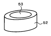
サファイア基板11上にLEDを構成するGaN系半導体層を成長させるのに用いるMOCVD装置を図4に示す。図4に示すように、このMOCVD装置においては、反応管51の下側に図5に示すようなサセプタ52が設けられている。このサセプタ52上に成長基板53が載置される。この場合、成長基板53はサファイア基板11である。このサセプタ52の内部にはヒータ(図示せず)が設けられており、このヒータにより成長基板53を必要な温度に加熱することができるようになっている。この場合、サセプタ52は成長基板53より十分に大きくし、反応管51の幅もサセプタ52より十分に大きくしてある。反応管51の上流部は仕切り板54で上下二つの部分に分けられている。そして、反応管51の上側のインレット55には十分に均一な流れの窒素または水素を導入し、下側のインレット56には十分に均一な流れのアンモニアおよび有機III族原料を導入する。
サセプタ52上の成長基板53の温度の面内分布を十分に小さく抑えるために、成長基板53は、図6Aに示すように、好適には、例えばSiCコートカーボン製で厚さが2mm以上の均熱板57上に載せ、均熱するのが有効である。あるいは、成長基板53としてのサファイア基板11が例えば0.4mm程度の厚さである場合には成長中に反ってしまい、それにより均熱板57から離れて温度の分布が生じるため、図6Bに示すように、成長基板53が成長中に反らないように十分な厚さ、例えば1mm程度の厚さにすることも有効である。さらに、図6Cに示すように、成長基板53が反ったときの形状に合わせて均熱板57の中心部分にくぼみを持たせ、成長基板53の裏面のすべてが均熱板57と接触するようにすることも有効である。この均熱板57のくぼみの形状は、例えば、活性層13の成長時の温度に加熱したときの成長基板53の反りに合わせるのが望ましい。
成長原料のV/III比の面内分布を十分に小さく抑えるためには、III族元素の原料とV族元素の原料との合流部分での合流を均一にしたり、反応管51を上記のように構成してIII族元素の原料とV族元素の原料とを下から合流させてそれを均一な層流にして流したり、反応管51の側面をサセプタ52から遠ざけたりすることが有効である。
FIG. 4 shows an MOCVD apparatus used for growing a GaN-based semiconductor layer constituting an LED on the
In order to keep the in-plane distribution of the temperature of the
In order to keep the in-plane distribution of the V / III ratio of the growth raw material sufficiently small, the merging of the group III element raw material and the group V element raw material is made uniform or the
このMOCVD装置においては、サセプタ52上の成長基板53の温度の面内分布は±1℃以内に抑えることができるとともに、成長基板53上に均一な層流内で成長を行うことができ、活性層13の厚さの面内分布を±2%以内に抑えることができ、さらに計算で求めた原料のV/III比の面内均一性も±2%以内であった。このようにして得られたGaN系LEDウェハは、緑色発光用のものとしては発光波長520nm±2nmの均一性をその外側から2mmの範囲を除いた部分で達成し、青色発光用のものとしては発光波長460nm±2nmの均一性をその外側から2mmの範囲を除いた部分で達成した。
一方、従来公知の方法で、例えばn型GaAs基板上にAlGaInP系半導体層を成長させて赤色発光AlGaInP系LEDウェハを製造する。
In this MOCVD apparatus, the in-plane distribution of the temperature of the
On the other hand, a red light emitting AlGaInP LED wafer is manufactured by growing an AlGaInP semiconductor layer on an n-type GaAs substrate, for example, by a conventionally known method.
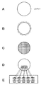
次に、上述のようにして製造された赤色発光AlGaInP系LEDウェハ、緑色発光GaN系LEDウェハおよび青色発光GaN系LEDウェハを分割してチップ化する。例えば、緑色発光GaN系LEDウェハについて具体的に説明する。まず、図7Aに示す緑色発光GaN系LEDウェハの縁から2mmの範囲内の外周部を図7Bに示すように研削して除去する。これは緑色発光GaN系LEDウェハの縁から2mmの範囲内の外周部は一般に半導体層の成長が不均一となり、この部分からは良好なLEDを作製することができないためである。次に、図7Cに示すように、緑色発光GaN系LEDウェハのダイシングを行って分割し、チップ化する。次に、図7Dおよび図7Eに示すように、ウェハの一部の領域から得られた緑色発光GaN系LEDを、矢印で示すようにウェハ内部における配列を維持したまま、透明なガラスやプラスチックからなる導光板101上にマウントする。より詳細には、それぞれの緑色発光GaN系LEDのウェハ内部における位置をメモリなどに記憶しておき、この位置情報に基づいてウェハ内部における配列順序を再現する形で導光板101上にマウントする。ここで、これらの緑色発光GaN系LEDはウェハの一部の領域から取り出されたものであるため、発光波長および発光強度とも±5nm以内に揃っている。赤色発光AlGaInP系LEDウェハおよび青色発光GaN系LEDウェハについても同様にしてチップ化し、ウェハー内部における配列を維持したまま導光板101上にマウントする。この場合、隣接して配列した赤色発光AlGaInP系LED、緑色発光GaN系LEDおよび青色発光GaN系LEDからなる3個のLEDにより一単位の発光部が構成され、この発光部が必要な数だけ二次元アレイ状に配列される。各LEDの大きさは例えば1mm角程度、そのときのLEDの配列ピッチは例えば20mm程度である。各LEDの大きさがより小さく例えば0.5mm角程度のとき、LEDの配列ピッチは例えば10mm程度である。各LEDの大きさがさらに小さく例えば0.1mm(100μm)角程度のとき、LEDの配列ピッチは例えば1mm程度である。各LEDの大きさが小さく、配列ピッチが短くなるにつれてLEDの個数が多くなるが、均一な発光が得られるという利点がある。
Next, the red light emitting AlGaInP LED wafer, the green light emitting GaN LED wafer, and the blue light emitting GaN LED wafer manufactured as described above are divided into chips. For example, a green light emitting GaN-based LED wafer will be specifically described. First, the outer peripheral portion within a range of 2 mm from the edge of the green light-emitting GaN-based LED wafer shown in FIG. 7A is ground and removed as shown in FIG. 7B. This is because the growth of the semiconductor layer is generally non-uniform in the outer peripheral portion within a range of 2 mm from the edge of the green light emitting GaN-based LED wafer, and a good LED cannot be produced from this portion. Next, as shown in FIG. 7C, the green light-emitting GaN-based LED wafer is diced and divided into chips. Next, as shown in FIGS. 7D and 7E, green light-emitting GaN-based LEDs obtained from a partial area of the wafer are made of transparent glass or plastic while maintaining the arrangement inside the wafer as indicated by arrows. Mount on the
図8にこのようにして得られたLEDバックライトを示す。導光板101には正方形または長方形の穴102が二次元アレイ状に設けられ、その穴102の中に各LEDがシリコーン樹脂などの接着剤によりマウントされる。符号103〜105がそれぞれ赤色発光AlGaInP系LED、緑色発光GaN系LEDおよび青色発光GaN系LEDを示す。図9に示すように、赤色発光AlGaInP系LED同士を直列に接続するように駆動用の配線106を形成し、緑色発光GaN系LED同士を直列に接続するように駆動用の配線107を形成し、青色発光GaN系LED同士を直列に接続するように駆動用の配線108を形成する。これらの配線106〜108に電流を流すことにより各LEDを発光させることができ、導光板101の後面から白色光が取り出され、バックライトを実現することができる。このLEDバックライトは液晶用バックライトとして用いて好適なものである。
FIG. 8 shows the LED backlight thus obtained. The
以上のように、この第1の実施形態によれば、同一のLEDウェハの一部の領域から得られた発光波長および発光強度が揃った赤色発光LED、緑色発光LEDおよび青色発光LEDをウェハ内部における配列を維持して導光板101上に配列することによりLEDバックライトを構成しているので、従来に比べて色および輝度の均一性が高い白色LEDバックライトを実現することができる。
As described above, according to the first embodiment, the red light emitting LED, the green light emitting LED, and the blue light emitting LED having the same light emission wavelength and light emission intensity obtained from a part of the same LED wafer are arranged inside the wafer. Since the LED backlight is configured by maintaining the arrangement in FIG. 5 and arranging it on the
次に、この発明の第2の実施形態によるLEDバックライトについて説明する。
この第2の実施形態においては、第1の実施形態と同様に工程を進めてパッド電極16まで形成した後、サファイア基板11の裏面側から例えばエキシマーレーザなどによるレーザビームを照射することにより、サファイア基板11から、n型GaN層12から上の部分を剥離する。この際、樹脂などでパッド電極16側を固定してから剥離を行うのが望ましい。図10にこのようにして得られるGaN系LEDを示す。
上記以外のことは、第1の実施形態と同様である。
この第2の実施形態によれば、第1の実施形態と同様な利点を得ることができる。
Next explained is an LED backlight according to the second embodiment of the invention.
In the second embodiment, the process proceeds to the
Other than the above are the same as in the first embodiment.
According to the second embodiment, the same advantages as those of the first embodiment can be obtained.
次に、この発明の第3の実施形態によるLEDバックライトについて説明する。
この第3の実施形態においては、第1の実施形態と同様に工程を進めてパッド電極16まで形成し、n型GaN層12上にn側電極17を形成しないで、サファイア基板11の裏面側から例えばエキシマーレーザなどによるレーザビームを照射することにより、サファイア基板11から、n型GaN層12から上の部分を剥離する。この際、樹脂などでパッド電極16側を固定してから剥離を行うのが望ましい。次に、このようにして剥離されたGaN系LEDウェハのn型GaN層12を裏面からHClなどを用いてウエットエッチングしたり、さらにラッピングを行ったりすることにより除去してn型GaN層12の裏面を露出させた後、この裏面にn側電極17を形成する。このn側電極17は例えばインジウム−スズ酸化物(ITO)、酸化ニッケル(NiO)、酸化亜鉛(ZnO)などからなる透明電極とし、この場合はn型GaN層12の裏面の全面にわたってn側電極17を形成することができる。図10にこのようにして得られるGaN系LEDを示す。
上記以外のことは、第1の実施形態と同様である。
この第3の実施形態によれば、第1の実施形態と同様な利点を得ることができる。
Next explained is an LED backlight according to the third embodiment of the invention.
In the third embodiment, the process proceeds to the
Other than the above are the same as in the first embodiment.
According to the third embodiment, the same advantages as those of the first embodiment can be obtained.
次に、この発明の第4の実施形態によるLEDバックライトについて説明する。
この第4の実施形態においては、第1の実施形態において、サファイア基板11上にMOCVD法によりGaN系半導体を成長させてGaN系LEDウェハを製造する場合に、MOCVD装置の反応管51内で成長中に成長基板53上に予期せぬ塵埃などの異物の付着が生じたことによりウェハ面内の成長温度の分布が正常時に比べて幾分悪化し、その結果、例えば緑色発光GaN系LEDウェハにおいては発光波長が520nm±2nmとなる範囲が中央部の半径10mmの範囲のみとなった場合を考える。
Next explained is an LED backlight according to the fourth embodiment of the invention.
In the fourth embodiment, in the first embodiment, when a GaN-based LED wafer is manufactured by growing a GaN-based semiconductor on the
この場合、図12Aに示す緑色発光GaN系LEDウェハの外周部を図12Bに示すように研削して除去し、中央部の半径10mmの部分のみ残す。次に、図12Cに示すように、こうして得られた半径10mmの緑色発光GaN系LEDウェハのダイシングを行って分割し、チップ化する。次に、図12Dおよび図12Eに示すように、このウェハの一部の領域から得られた緑色発光GaN系LEDを、矢印で示すようにウェハ内部における配列を維持したまま導光板101上にマウントする。より詳細には、それぞれの緑色発光GaN系LEDのウェハ内部における位置をメモリなどに記憶しておき、この位置情報に基づいてウェハ内部における配列順序を再現する形で導光板101上にマウントする。ここで、これらの緑色発光GaN系LEDはウェハの一部の領域から取り出されたものであるため、発光波長および発光強度とも±5nm以内に揃っている。
上記以外のことは、第1の実施形態と同様である。
この第4の実施形態によれば、第1の実施形態と同様な利点を得ることができる。
In this case, the outer peripheral portion of the green light-emitting GaN-based LED wafer shown in FIG. 12A is removed by grinding as shown in FIG. 12B, leaving only the central portion having a radius of 10 mm. Next, as shown in FIG. 12C, the green light-emitting GaN-based LED wafer having a radius of 10 mm obtained in this way is diced and divided into chips. Next, as shown in FIG. 12D and FIG. 12E, green light-emitting GaN-based LEDs obtained from a part of the wafer are mounted on the
Other than the above are the same as in the first embodiment.
According to the fourth embodiment, the same advantages as those of the first embodiment can be obtained.
次に、この発明の第5の実施形態によるLEDディスプレイについて説明する。
この第5の実施形態においては、図13Aに示す緑色発光GaN系LEDウェハの縁から2mmの範囲内の外周部を図13Bに示すように研削して除去する。次に、図13Cに示すように、緑色発光GaN系LEDウェハのダイシングを行って分割し、チップ化する。次に、図13Dおよび図13Eに示すように、ウェハの一部の領域から得られた緑色発光GaN系LEDを、矢印で示すようにウェハ内部における配列を維持したまま導光板101上にマウントする。より詳細には、それぞれの緑色発光GaN系LEDのウェハ内部における位置をメモリなどに記憶しておき、この位置情報に基づいてウェハ内部における配列順序を再現する形で導光板101上にマウントする。ここで、これらの緑色発光GaN系LEDはウェハの一部の領域から取り出されたものであるため、発光波長および発光強度とも±5nm以内に揃っている。赤色発光AlGaInP系LEDウェハおよび青色発光GaN系LEDウェハについても同様にしてチップ化し、ウェハー内部における配列を維持したまま導光板101上にマウントする。この場合、隣接して配列した赤色発光AlGaInP系LED、緑色発光GaN系LEDおよび青色発光GaN系LEDからなる3個のLEDにより一画素が構成され、この画素が必要な数だけ二次元アレイ状に配列される。各LEDの大きさは例えば0.5mm角程度である。LEDの配列ピッチは例えば10mm程度である。
Next explained is an LED display according to the fifth embodiment of the invention.
In the fifth embodiment, the outer peripheral portion within a range of 2 mm from the edge of the green light emitting GaN-based LED wafer shown in FIG. 13A is removed by grinding as shown in FIG. 13B. Next, as shown in FIG. 13C, the green light-emitting GaN-based LED wafer is diced and divided into chips. Next, as shown in FIGS. 13D and 13E, green light-emitting GaN-based LEDs obtained from a partial region of the wafer are mounted on the
図14にこのようにして得られたLEDディスプレイを示す。導光板101には正方形または長方形の穴102が二次元アレイ状に設けられ、その穴102の中に各LEDがシリコーン樹脂などの接着剤によりマウントされる。符号103〜105がそれぞれ赤色発光AlGaInP系LED、緑色発光GaN系LEDおよび青色発光GaN系LEDを示す。図15に示すように、各LEDを駆動するために、各LEDのp側電極15上のパッド電極16間を接続する配線106を形成するとともに、各LEDのn側電極17間を接続する配線107を形成する。これらの配線106、107を線順次駆動することで各LEDを発光させ、パッシブマトリックス駆動することができ、フルカラーLEDディスプレイを実現することができる。
FIG. 14 shows the LED display thus obtained. The
以上のように、この第5の実施形態によれば、同一のLEDウェハの一部の領域から得られた発光波長および発光強度が揃った赤色発光LED、緑色発光LEDおよび青色発光LEDをウェハ内部における配列を維持して導光板101上に配列することによりLEDディスプレイを構成しているので、従来に比べて色および輝度の均一性が高いフルカラーLEDディスプレイを実現することができる。
As described above, according to the fifth embodiment, the red light emitting LED, the green light emitting LED, and the blue light emitting LED having the same emission wavelength and emission intensity obtained from a part of the same LED wafer are arranged inside the wafer. Since the LED display is configured by maintaining the arrangement in FIG. 5 and arranging it on the
以上、この発明の実施形態について具体的に説明したが、この発明は、上述の実施形態に限定されるものではなく、この発明の技術的思想に基づく各種の変形が可能である。
例えば、上述の第1〜第5の実施形態において挙げた数値、材料、構造、形状、基板、原料、プロセスなどはあくまでも例に過ぎず、必要に応じて、これらと異なる数値、材料、構造、形状、基板、原料、プロセスなどを用いてもよい。
As mentioned above, although embodiment of this invention was described concretely, this invention is not limited to the above-mentioned embodiment, The various deformation | transformation based on the technical idea of this invention is possible.
For example, the numerical values, materials, structures, shapes, substrates, raw materials, processes, etc. given in the first to fifth embodiments are merely examples, and if necessary, numerical values, materials, structures, Shapes, substrates, raw materials, processes, etc. may be used.
例えば、第1の実施形態においては、ウェハの一部の領域から得られた緑色発光GaN系LEDを、ウェハ内部における配列を維持したまま導光板101上にマウントしているが、必ずしもウェハ内部における配列を維持したままマウントする必要はなく、一部のLEDの配列順を変えてマウントするようにしてもよい。
また、例えば、第1〜第5の実施形態において、LEDを構成する半導体層の積層構造や形状は単なる例に過ぎず、他の積層構造や形状であってもよい。
また、第1〜第5の実施形態においては、成長基板としてサファイア基板を用いているが、必要に応じて、すでに述べたSiC基板、Si基板などの他の基板を用いてもよい。
For example, in the first embodiment, green light-emitting GaN-based LEDs obtained from a partial area of the wafer are mounted on the
Further, for example, in the first to fifth embodiments, the laminated structure and shape of the semiconductor layers constituting the LED are merely examples, and other laminated structures and shapes may be used.
In the first to fifth embodiments, the sapphire substrate is used as the growth substrate, but other substrates such as the SiC substrate and the Si substrate described above may be used as necessary.
さらに、上述の第1〜第5の実施形態において、p側電極15の材料として例えばAuやAgなどを用いるとともに、p型GaN層14とp側電極15との間に活性層13で発生した光の侵入長以下の厚さを有し、Ni、Pd、Co、Sbなどからなるコンタクト金属層を形成してもよい。このようにすることにより、コンタクト金属層による反射増強効果で、GaN系LEDの発光効率のより一層の向上を図ることができる。
また、上述の第5の実施形態において、各LEDの裏面側にレンズを設け、LEDから発光する光をこのレンズで集光してから導光板101を通して外部に取り出すようにしてもよい。光取り出し効率を高くするために、樹脂などの屈折率が1以上の物質でLEDの裏面側を覆うようにしてもよい。
Further, in the first to fifth embodiments described above, for example, Au or Ag is used as the material of the p-
In the fifth embodiment described above, a lens may be provided on the back side of each LED, and light emitted from the LED may be collected by this lens and then taken out through the
11…サファイア基板、12…n型GaN層、13…活性層、14…p型GaN層、15…p側電極、16…パッド電極、17…n側電極、51…反応管、52…サセプタ、53…成長基板、54…仕切り板、101…導光板、102…穴、103…赤色発光AlGaInP系LED、104…緑色発光GaN系LED、105…青色発光GaN系LED、106〜108…配線
DESCRIPTION OF
Claims (27)
上記赤色発光の発光ダイオード、上記緑色発光の発光ダイオードおよび上記青色発光の発光ダイオードのうちの少なくとも一種類の発光ダイオードが、同一の発光ダイオードウェハから得られたものである
ことを特徴とする発光ダイオードバックライト。 In a light emitting diode backlight formed by arranging a plurality of red light emitting diodes, green light emitting diodes and blue light emitting diodes on a substrate,
The light emitting diode, wherein at least one of the red light emitting diode, the green light emitting diode, and the blue light emitting diode is obtained from the same light emitting diode wafer. Backlight.
上記赤色発光の発光ダイオード、上記緑色発光の発光ダイオードおよび上記青色発光の発光ダイオードのうちの少なくとも一種類の発光ダイオードが、同一の発光ダイオードウェハから得られた複数の発光ダイオードがその内部における配列を維持して上記基板上に配列されたものである
ことを特徴とする発光ダイオードバックライト。 In a light emitting diode backlight formed by arranging a plurality of red light emitting diodes, green light emitting diodes and blue light emitting diodes on a substrate,
A plurality of light emitting diodes obtained from the same light emitting diode wafer are arranged in at least one of the red light emitting diode, the green light emitting diode, and the blue light emitting diode. A light-emitting diode backlight, which is maintained and arranged on the substrate.
上記赤色発光の発光ダイオード、上記緑色発光の発光ダイオードおよび上記青色発光の発光ダイオードのうちの少なくとも上記緑色発光の発光ダイオードおよび上記青色発光の発光ダイオードが、それぞれ同一の発光ダイオードウェハから得られた複数の発光ダイオードがその内部における配列を維持して上記基板上に配列されたものである
ことを特徴とする発光ダイオードバックライト。 In a light emitting diode backlight formed by arranging a plurality of red light emitting diodes, green light emitting diodes and blue light emitting diodes on a substrate,
A plurality of at least the green light emitting diode and the blue light emitting diode among the red light emitting diode, the green light emitting diode, and the blue light emitting diode, each obtained from the same light emitting diode wafer. The light-emitting diode backlight is characterized in that the light-emitting diodes are arranged on the substrate while maintaining the arrangement therein.
上記赤色発光の発光ダイオード、上記緑色発光の発光ダイオードおよび上記青色発光の発光ダイオードのうちの少なくとも一種類の発光ダイオードとして、同一の発光ダイオードウェハから得られたものを用いる
ことを特徴とする発光ダイオードバックライトの製造方法。 In a method of manufacturing a light emitting diode backlight formed by arranging a plurality of red light emitting diodes, green light emitting diodes and blue light emitting diodes on a substrate, respectively,
A light emitting diode obtained from the same light emitting diode wafer is used as at least one kind of light emitting diode of the red light emitting diode, the green light emitting diode and the blue light emitting diode. Manufacturing method of backlight.
上記赤色発光の発光ダイオード、上記緑色発光の発光ダイオードおよび上記青色発光の発光ダイオードのうちの少なくとも一種類の発光ダイオードとして、同一の発光ダイオードウェハから得られた複数の発光ダイオードをその内部における配列を維持して上記基板上に配列する
ことを特徴とする発光ダイオードバックライトの製造方法。 In a method of manufacturing a light emitting diode backlight formed by arranging a plurality of red light emitting diodes, green light emitting diodes and blue light emitting diodes on a substrate, respectively,
A plurality of light emitting diodes obtained from the same light emitting diode wafer are arranged as at least one of the red light emitting diode, the green light emitting diode and the blue light emitting diode. A method of manufacturing a light-emitting diode backlight, comprising maintaining and arranging on the substrate.
上記赤色発光の発光ダイオード、上記緑色発光の発光ダイオードおよび上記青色発光の発光ダイオードのうちの少なくとも上記緑色発光の発光ダイオードおよび上記青色発光の発光ダイオードとして、それぞれ同一の発光ダイオードウェハから得られた複数の発光ダイオードをその内部における配列を維持して上記基板上に配列する
ことを特徴とする発光ダイオードバックライトの製造方法。 In a method of manufacturing a light emitting diode backlight formed by arranging a plurality of red light emitting diodes, green light emitting diodes and blue light emitting diodes on a substrate, respectively,
A plurality of at least one of the red light emitting diode, the green light emitting diode, and the blue light emitting diode, each obtained from the same light emitting diode wafer, as the green light emitting diode and the blue light emitting diode. A method for producing a light-emitting diode backlight, comprising: arranging the light-emitting diodes on the substrate while maintaining an arrangement inside the light-emitting diodes.
上記赤色発光の発光ダイオード、上記緑色発光の発光ダイオードおよび上記青色発光の発光ダイオードのうちの少なくとも一種類の発光ダイオードが、同一の発光ダイオードウェハから得られたものである
ことを特徴とする発光ダイオードディスプレイ。 In a light emitting diode display formed by arranging a plurality of red light emitting diodes, green light emitting diodes and blue light emitting diodes on a substrate,
The light emitting diode, wherein at least one of the red light emitting diode, the green light emitting diode, and the blue light emitting diode is obtained from the same light emitting diode wafer. display.
上記赤色発光の発光ダイオード、上記緑色発光の発光ダイオードおよび上記青色発光の発光ダイオードのうちの少なくとも一種類の発光ダイオードが、同一の発光ダイオードウェハから得られた複数の発光ダイオードがその内部における配列を維持して上記基板上に配列されたものである
ことを特徴とする発光ダイオードディスプレイ。 In a light emitting diode display formed by arranging a plurality of red light emitting diodes, green light emitting diodes and blue light emitting diodes on a substrate,
A plurality of light emitting diodes obtained from the same light emitting diode wafer are arranged in at least one of the red light emitting diode, the green light emitting diode, and the blue light emitting diode. A light-emitting diode display which is maintained and arranged on the substrate.
上記赤色発光の発光ダイオード、上記緑色発光の発光ダイオードおよび上記青色発光の発光ダイオードのうちの少なくとも上記緑色発光の発光ダイオードおよび上記青色発光の発光ダイオードが、それぞれ同一の発光ダイオードウェハから得られた複数の発光ダイオードがその内部における配列を維持して上記基板上に配列されたものである
ことを特徴とする発光ダイオードディスプレイ。 In a light emitting diode display formed by arranging a plurality of red light emitting diodes, green light emitting diodes and blue light emitting diodes on a substrate,
A plurality of at least the green light emitting diode and the blue light emitting diode among the red light emitting diode, the green light emitting diode, and the blue light emitting diode, each obtained from the same light emitting diode wafer. A light-emitting diode display, wherein the light-emitting diodes are arranged on the substrate while maintaining the arrangement in the inside thereof.
上記赤色発光の発光ダイオード、上記緑色発光の発光ダイオードおよび上記青色発光の発光ダイオードのうちの少なくとも一種類の発光ダイオードとして、同一の発光ダイオードウェハから得られたものを用いる
ことを特徴とする発光ダイオードディスプレイの製造方法。 In a method of manufacturing a light emitting diode display formed by arranging a plurality of red light emitting diodes, green light emitting diodes and blue light emitting diodes on a substrate, respectively,
A light emitting diode obtained from the same light emitting diode wafer is used as at least one kind of light emitting diode of the red light emitting diode, the green light emitting diode and the blue light emitting diode. Display manufacturing method.
上記赤色発光の発光ダイオード、上記緑色発光の発光ダイオードおよび上記青色発光の発光ダイオードのうちの少なくとも一種類の発光ダイオードとして、同一の発光ダイオードウェハから得られた複数の発光ダイオードをその内部における配列を維持して上記基板上に配列する
ことを特徴とする発光ダイオードディスプレイの製造方法。 In a method of manufacturing a light emitting diode display formed by arranging a plurality of red light emitting diodes, green light emitting diodes and blue light emitting diodes on a substrate, respectively,
A plurality of light emitting diodes obtained from the same light emitting diode wafer are arranged as at least one of the red light emitting diode, the green light emitting diode and the blue light emitting diode. A method for producing a light-emitting diode display, comprising maintaining and arranging on the substrate.
上記赤色発光の発光ダイオード、上記緑色発光の発光ダイオードおよび上記青色発光の発光ダイオードのうちの少なくとも上記緑色発光の発光ダイオードおよび上記青色発光の発光ダイオードとして、それぞれ同一の発光ダイオードウェハから得られた複数の発光ダイオードをその内部における配列を維持して上記基板上に配列する
ことを特徴とする発光ダイオードディスプレイの製造方法。 In a method of manufacturing a light emitting diode display formed by arranging a plurality of red light emitting diodes, green light emitting diodes and blue light emitting diodes on a substrate, respectively,
A plurality of at least one of the red light emitting diode, the green light emitting diode, and the blue light emitting diode, each obtained from the same light emitting diode wafer, as the green light emitting diode and the blue light emitting diode. A method for manufacturing a light emitting diode display, comprising: arranging the light emitting diodes on the substrate while maintaining an arrangement in the inside thereof.
上記赤色発光の発光ダイオード、上記緑色発光の発光ダイオードおよび上記青色発光の発光ダイオードのうちの少なくとも一種類の発光ダイオードが、同一の発光ダイオードウェハから得られたものである
ことを特徴とする発光ダイオード照明装置。 In a light emitting diode illuminating device formed by arranging a plurality of red light emitting diodes, green light emitting diodes and blue light emitting diodes on a substrate,
The light emitting diode, wherein at least one of the red light emitting diode, the green light emitting diode, and the blue light emitting diode is obtained from the same light emitting diode wafer. Lighting device.
上記赤色発光の発光ダイオード、上記緑色発光の発光ダイオードおよび上記青色発光の発光ダイオードのうちの少なくとも一種類の発光ダイオードが、同一の発光ダイオードウェハから得られた複数の発光ダイオードがその内部における配列を維持して上記基板上に配列されたものである
ことを特徴とする発光ダイオード照明装置。 In a light emitting diode illuminating device formed by arranging a plurality of red light emitting diodes, green light emitting diodes and blue light emitting diodes on a substrate,
A plurality of light emitting diodes obtained from the same light emitting diode wafer are arranged in at least one of the red light emitting diode, the green light emitting diode, and the blue light emitting diode. A light-emitting diode illuminating device, which is maintained and arranged on the substrate.
上記赤色発光の発光ダイオード、上記緑色発光の発光ダイオードおよび上記青色発光の発光ダイオードのうちの少なくとも上記緑色発光の発光ダイオードおよび上記青色発光の発光ダイオードが、それぞれ同一の発光ダイオードウェハから得られた複数の発光ダイオードがその内部における配列を維持して上記基板上に配列されたものである
ことを特徴とする発光ダイオード照明装置。 In a light emitting diode illuminating device formed by arranging a plurality of red light emitting diodes, green light emitting diodes and blue light emitting diodes on a substrate,
A plurality of at least the green light emitting diode and the blue light emitting diode among the red light emitting diode, the green light emitting diode, and the blue light emitting diode, each obtained from the same light emitting diode wafer. The light-emitting diode illuminating device is characterized in that the light-emitting diodes are arranged on the substrate while maintaining the arrangement in the inside thereof.
上記赤色発光の発光ダイオード、上記緑色発光の発光ダイオードおよび上記青色発光の発光ダイオードのうちの少なくとも一種類の発光ダイオードとして、同一の発光ダイオードウェハから得られたものを用いる
ことを特徴とする発光ダイオード照明装置の製造方法。 In a method for manufacturing a light emitting diode illumination device formed by arranging a plurality of red light emitting diodes, green light emitting diodes and blue light emitting diodes on a substrate,
A light emitting diode obtained from the same light emitting diode wafer is used as at least one kind of light emitting diode of the red light emitting diode, the green light emitting diode and the blue light emitting diode. Manufacturing method of lighting device.
上記赤色発光の発光ダイオード、上記緑色発光の発光ダイオードおよび上記青色発光の発光ダイオードのうちの少なくとも一種類の発光ダイオードとして、同一の発光ダイオードウェハから得られた複数の発光ダイオードをその内部における配列を維持して上記基板上に配列する
ことを特徴とする発光ダイオード照明装置の製造方法。 In a method for manufacturing a light emitting diode illumination device formed by arranging a plurality of red light emitting diodes, green light emitting diodes and blue light emitting diodes on a substrate,
A plurality of light emitting diodes obtained from the same light emitting diode wafer are arranged as at least one of the red light emitting diode, the green light emitting diode and the blue light emitting diode. A method of manufacturing a light-emitting diode illuminating device, comprising maintaining and arranging on the substrate.
上記赤色発光の発光ダイオード、上記緑色発光の発光ダイオードおよび上記青色発光の発光ダイオードのうちの少なくとも上記緑色発光の発光ダイオードおよび上記青色発光の発光ダイオードとして、それぞれ同一の発光ダイオードウェハから得られた複数の発光ダイオードをその内部における配列を維持して上記基板上に配列する
ことを特徴とする発光ダイオード照明装置の製造方法。 In a method for manufacturing a light emitting diode illumination device formed by arranging a plurality of red light emitting diodes, green light emitting diodes and blue light emitting diodes on a substrate,
A plurality of at least one of the red light emitting diode, the green light emitting diode, and the blue light emitting diode, each obtained from the same light emitting diode wafer, as the green light emitting diode and the blue light emitting diode. A method for manufacturing a light-emitting diode illuminating device, comprising: arranging the light-emitting diodes on the substrate while maintaining an arrangement inside the light-emitting diodes.
上記赤色発光の発光ダイオード、上記緑色発光の発光ダイオードおよび上記青色発光の発光ダイオードのうちの少なくとも一種類の発光ダイオードが、同一の発光ダイオードウェハから得られたものである
ことを特徴とする発光ダイオードアレイ装置。 In a light emitting diode array device formed by arranging a plurality of red light emitting diodes, green light emitting diodes and blue light emitting diodes on a substrate,
The light emitting diode, wherein at least one of the red light emitting diode, the green light emitting diode, and the blue light emitting diode is obtained from the same light emitting diode wafer. Array device.
上記赤色発光の発光ダイオード、上記緑色発光の発光ダイオードおよび上記青色発光の発光ダイオードのうちの少なくとも一種類の発光ダイオードが、同一の発光ダイオードウェハから得られた複数の発光ダイオードがその内部における配列を維持して上記基板上に配列されたものである
ことを特徴とする発光ダイオードアレイ装置。 In a light emitting diode array device formed by arranging a plurality of red light emitting diodes, green light emitting diodes and blue light emitting diodes on a substrate,
A plurality of light emitting diodes obtained from the same light emitting diode wafer are arranged in at least one of the red light emitting diode, the green light emitting diode, and the blue light emitting diode. A light-emitting diode array device that is maintained and arranged on the substrate.
上記赤色発光の発光ダイオード、上記緑色発光の発光ダイオードおよび上記青色発光の発光ダイオードのうちの少なくとも上記緑色発光の発光ダイオードおよび上記青色発光の発光ダイオードが、それぞれ同一の発光ダイオードウェハから得られた複数の発光ダイオードがその内部における配列を維持して上記基板上に配列されたものである
ことを特徴とする発光ダイオードアレイ装置。 In a light emitting diode array device formed by arranging a plurality of red light emitting diodes, green light emitting diodes and blue light emitting diodes on a substrate,
A plurality of at least the green light emitting diode and the blue light emitting diode among the red light emitting diode, the green light emitting diode, and the blue light emitting diode, each obtained from the same light emitting diode wafer. The light-emitting diode array device is characterized in that the light-emitting diodes are arranged on the substrate while maintaining the arrangement in the inside thereof.
上記赤色発光の発光ダイオード、上記緑色発光の発光ダイオードおよび上記青色発光の発光ダイオードのうちの少なくとも一種類の発光ダイオードとして、同一の発光ダイオードウェハから得られたものを用いる
ことを特徴とする発光ダイオードアレイ装置の製造方法。 In a method of manufacturing a light emitting diode array device formed by arranging a plurality of red light emitting diodes, green light emitting diodes and blue light emitting diodes on a substrate,
A light emitting diode obtained from the same light emitting diode wafer is used as at least one kind of light emitting diode of the red light emitting diode, the green light emitting diode and the blue light emitting diode. A method for manufacturing an array device.
上記赤色発光の発光ダイオード、上記緑色発光の発光ダイオードおよび上記青色発光の発光ダイオードのうちの少なくとも一種類の発光ダイオードとして、同一の発光ダイオードウェハから得られた複数の発光ダイオードをその内部における配列を維持して上記基板上に配列する
ことを特徴とする発光ダイオードアレイ装置の製造方法。 In a method of manufacturing a light emitting diode array device formed by arranging a plurality of red light emitting diodes, green light emitting diodes and blue light emitting diodes on a substrate,
A plurality of light emitting diodes obtained from the same light emitting diode wafer are arranged as at least one of the red light emitting diode, the green light emitting diode and the blue light emitting diode. A method of manufacturing a light-emitting diode array device, comprising maintaining and arranging on the substrate.
上記赤色発光の発光ダイオード、上記緑色発光の発光ダイオードおよび上記青色発光の発光ダイオードのうちの少なくとも上記緑色発光の発光ダイオードおよび上記青色発光の発光ダイオードとして、それぞれ同一の発光ダイオードウェハから得られた複数の発光ダイオードをその内部における配列を維持して上記基板上に配列する
ことを特徴とする発光ダイオードアレイ装置の製造方法。
In a method of manufacturing a light emitting diode array device formed by arranging a plurality of red light emitting diodes, green light emitting diodes and blue light emitting diodes on a substrate,
A plurality of at least one of the red light emitting diode, the green light emitting diode, and the blue light emitting diode, each obtained from the same light emitting diode wafer, as the green light emitting diode and the blue light emitting diode. A method for manufacturing a light-emitting diode array device, comprising: arranging the light-emitting diodes on the substrate while maintaining the arrangement inside the light-emitting diodes.
Priority Applications (1)
| Application Number | Priority Date | Filing Date | Title |
|---|---|---|---|
| JP2004278684A JP2006093490A (en) | 2004-09-27 | 2004-09-27 | Light emitting diode back panel and its manufacturing method, light emitting diode display and its manufacturing method, light emitting diode lighting device and its manufacturing method, and light emitting diode array device and its manufacturing method |
Applications Claiming Priority (1)
| Application Number | Priority Date | Filing Date | Title |
|---|---|---|---|
| JP2004278684A JP2006093490A (en) | 2004-09-27 | 2004-09-27 | Light emitting diode back panel and its manufacturing method, light emitting diode display and its manufacturing method, light emitting diode lighting device and its manufacturing method, and light emitting diode array device and its manufacturing method |
Publications (2)
| Publication Number | Publication Date |
|---|---|
| JP2006093490A true JP2006093490A (en) | 2006-04-06 |
| JP2006093490A5 JP2006093490A5 (en) | 2007-10-18 |
Family
ID=36234153
Family Applications (1)
| Application Number | Title | Priority Date | Filing Date |
|---|---|---|---|
| JP2004278684A Pending JP2006093490A (en) | 2004-09-27 | 2004-09-27 | Light emitting diode back panel and its manufacturing method, light emitting diode display and its manufacturing method, light emitting diode lighting device and its manufacturing method, and light emitting diode array device and its manufacturing method |
Country Status (1)
| Country | Link |
|---|---|
| JP (1) | JP2006093490A (en) |
Cited By (1)
| Publication number | Priority date | Publication date | Assignee | Title |
|---|---|---|---|---|
| JP2021027085A (en) * | 2019-07-31 | 2021-02-22 | 日亜化学工業株式会社 | Light-emitting module, method for manufacturing the same, and liquid crystal display device |
Citations (4)
| Publication number | Priority date | Publication date | Assignee | Title |
|---|---|---|---|---|
| JPH0661573A (en) * | 1992-08-06 | 1994-03-04 | Fujitsu Ltd | Manufacture of optical semiconductor device |
| JPH118438A (en) * | 1997-06-16 | 1999-01-12 | Furukawa Electric Co Ltd:The | Manufacture of semiconductor laser device |
| JP2002118124A (en) * | 2000-10-06 | 2002-04-19 | Sony Corp | Device mounting method |
| JP2002231543A (en) * | 2001-01-31 | 2002-08-16 | Diamond Electric Mfg Co Ltd | Ignition coil for internal combustion engine |
-
2004
- 2004-09-27 JP JP2004278684A patent/JP2006093490A/en active Pending
Patent Citations (4)
| Publication number | Priority date | Publication date | Assignee | Title |
|---|---|---|---|---|
| JPH0661573A (en) * | 1992-08-06 | 1994-03-04 | Fujitsu Ltd | Manufacture of optical semiconductor device |
| JPH118438A (en) * | 1997-06-16 | 1999-01-12 | Furukawa Electric Co Ltd:The | Manufacture of semiconductor laser device |
| JP2002118124A (en) * | 2000-10-06 | 2002-04-19 | Sony Corp | Device mounting method |
| JP2002231543A (en) * | 2001-01-31 | 2002-08-16 | Diamond Electric Mfg Co Ltd | Ignition coil for internal combustion engine |
Cited By (3)
| Publication number | Priority date | Publication date | Assignee | Title |
|---|---|---|---|---|
| JP2021027085A (en) * | 2019-07-31 | 2021-02-22 | 日亜化学工業株式会社 | Light-emitting module, method for manufacturing the same, and liquid crystal display device |
| US11181772B2 (en) * | 2019-07-31 | 2021-11-23 | Nichia Corporation | Light-emitting module, method for manufacturing the same, and liquid-crystal display device |
| US11506933B2 (en) | 2019-07-31 | 2022-11-22 | Nichia Corporation | Light-emitting module, method for manufacturing the same, and liquid-crystal display device |
Similar Documents
| Publication | Publication Date | Title |
|---|---|---|
| JP4223797B2 (en) | Nitride-based semiconductor light-emitting device and manufacturing method thereof | |
| US8124990B2 (en) | Semiconductor light emitting device having an electron barrier layer between a plurality of active layers | |
| CN101379627B (en) | Light emitting element | |
| JP5082278B2 (en) | Light emitting diode manufacturing method, integrated light emitting diode manufacturing method, and nitride III-V compound semiconductor growth method | |
| JP4687109B2 (en) | Manufacturing method of integrated light emitting diode | |
| JP5083817B2 (en) | Group III nitride semiconductor light-emitting device and method for manufacturing the same | |
| KR101077078B1 (en) | Gallium nitride compound semiconductor light emitting element | |
| EP2333836B1 (en) | Light-emitting device | |
| US20080315180A1 (en) | Semiconductor light emitting device | |
| CN103325899A (en) | White light emitting diode | |
| JP2003068109A (en) | Luminaire and projector | |
| KR100661960B1 (en) | Light emitting diode and manufacturing method thereof | |
| JP2008091942A (en) | Nitride semiconductor light emitting diode | |
| US10096646B2 (en) | Light-emitting unit | |
| JP4735037B2 (en) | LIGHT EMITTING DIODE AND ITS MANUFACTURING METHOD, INTEGRATED LIGHT EMITTING DIODE AND ITS MANUFACTURING METHOD, LIGHT EMITTING DIODE BACKLIGHT, LIGHT EMITTING DIODE LIGHTING DEVICE, LIGHT EMITTING DIODE DISPLAY AND ELECTRONIC | |
| JP5140979B2 (en) | AlGaInP light emitting diode, light source cell unit, display and electronic device | |
| JP4074315B2 (en) | Nitride semiconductor light emitting diode | |
| KR20130075321A (en) | Light emitting device | |
| JP2002305327A (en) | Nitride-based semiconductor light emitting device | |
| JP2006093490A (en) | Light emitting diode back panel and its manufacturing method, light emitting diode display and its manufacturing method, light emitting diode lighting device and its manufacturing method, and light emitting diode array device and its manufacturing method | |
| KR101709991B1 (en) | Light emitting device and fabrication method thereof | |
| KR20080024787A (en) | Semiconductor light-emitting device and manufacturing method thereof | |
| JP2006147679A (en) | Integrated light emitting diode, manufacturing method thereof, display and lighting apparatus for light emitting diode | |
| KR20130053512A (en) | Light emitting device | |
| KR20130075326A (en) | Light emitting device |
Legal Events
| Date | Code | Title | Description |
|---|---|---|---|
| A521 | Written amendment |
Free format text: JAPANESE INTERMEDIATE CODE: A523 Effective date: 20070831 |
|
| A621 | Written request for application examination |
Free format text: JAPANESE INTERMEDIATE CODE: A621 Effective date: 20070831 |
|
| A977 | Report on retrieval |
Free format text: JAPANESE INTERMEDIATE CODE: A971007 Effective date: 20100406 |
|
| A131 | Notification of reasons for refusal |
Free format text: JAPANESE INTERMEDIATE CODE: A131 Effective date: 20100928 |
|
| A521 | Written amendment |
Free format text: JAPANESE INTERMEDIATE CODE: A523 Effective date: 20101117 |
|
| A131 | Notification of reasons for refusal |
Free format text: JAPANESE INTERMEDIATE CODE: A131 Effective date: 20110301 |
|
| A02 | Decision of refusal |
Free format text: JAPANESE INTERMEDIATE CODE: A02 Effective date: 20110628 |