JP2006080247A - Semiconductor device - Google Patents
Semiconductor device Download PDFInfo
- Publication number
- JP2006080247A JP2006080247A JP2004261751A JP2004261751A JP2006080247A JP 2006080247 A JP2006080247 A JP 2006080247A JP 2004261751 A JP2004261751 A JP 2004261751A JP 2004261751 A JP2004261751 A JP 2004261751A JP 2006080247 A JP2006080247 A JP 2006080247A
- Authority
- JP
- Japan
- Prior art keywords
- well
- semiconductor device
- misfet
- data
- nonvolatile memory
- Prior art date
- Legal status (The legal status is an assumption and is not a legal conclusion. Google has not performed a legal analysis and makes no representation as to the accuracy of the status listed.)
- Granted
Links
- 239000004065 semiconductor Substances 0.000 title claims abstract description 162
- 230000015556 catabolic process Effects 0.000 claims abstract description 12
- 239000000758 substrate Substances 0.000 claims description 29
- 238000002955 isolation Methods 0.000 claims description 28
- 239000002784 hot electron Substances 0.000 claims description 7
- 239000003990 capacitor Substances 0.000 claims description 4
- 238000004519 manufacturing process Methods 0.000 abstract description 21
- 238000000034 method Methods 0.000 abstract description 19
- 230000008569 process Effects 0.000 abstract description 6
- 230000000295 complement effect Effects 0.000 abstract description 3
- 230000006378 damage Effects 0.000 abstract 1
- 238000006731 degradation reaction Methods 0.000 abstract 1
- 239000010410 layer Substances 0.000 description 23
- VYPSYNLAJGMNEJ-UHFFFAOYSA-N Silicium dioxide Chemical compound O=[Si]=O VYPSYNLAJGMNEJ-UHFFFAOYSA-N 0.000 description 17
- 229910052814 silicon oxide Inorganic materials 0.000 description 17
- 229910021332 silicide Inorganic materials 0.000 description 14
- FVBUAEGBCNSCDD-UHFFFAOYSA-N silicide(4-) Chemical compound [Si-4] FVBUAEGBCNSCDD-UHFFFAOYSA-N 0.000 description 14
- 239000012535 impurity Substances 0.000 description 13
- 230000002093 peripheral effect Effects 0.000 description 9
- 238000005229 chemical vapour deposition Methods 0.000 description 8
- 239000010936 titanium Substances 0.000 description 7
- 229910052581 Si3N4 Inorganic materials 0.000 description 6
- NRTOMJZYCJJWKI-UHFFFAOYSA-N Titanium nitride Chemical compound [Ti]#N NRTOMJZYCJJWKI-UHFFFAOYSA-N 0.000 description 6
- 230000006866 deterioration Effects 0.000 description 6
- HQVNEWCFYHHQES-UHFFFAOYSA-N silicon nitride Chemical compound N12[Si]34N5[Si]62N3[Si]51N64 HQVNEWCFYHHQES-UHFFFAOYSA-N 0.000 description 6
- 230000000694 effects Effects 0.000 description 5
- 230000005684 electric field Effects 0.000 description 5
- 238000005530 etching Methods 0.000 description 5
- 229910052796 boron Inorganic materials 0.000 description 4
- 238000001312 dry etching Methods 0.000 description 4
- 230000006870 function Effects 0.000 description 4
- 230000014759 maintenance of location Effects 0.000 description 4
- 229920002120 photoresistant polymer Polymers 0.000 description 4
- 229910021420 polycrystalline silicon Inorganic materials 0.000 description 4
- 125000006850 spacer group Chemical group 0.000 description 4
- ZOXJGFHDIHLPTG-UHFFFAOYSA-N Boron Chemical compound [B] ZOXJGFHDIHLPTG-UHFFFAOYSA-N 0.000 description 3
- 229910052785 arsenic Inorganic materials 0.000 description 3
- 230000007547 defect Effects 0.000 description 3
- 238000009413 insulation Methods 0.000 description 3
- 238000005468 ion implantation Methods 0.000 description 3
- PXHVJJICTQNCMI-UHFFFAOYSA-N nickel Substances [Ni] PXHVJJICTQNCMI-UHFFFAOYSA-N 0.000 description 3
- 229910052698 phosphorus Inorganic materials 0.000 description 3
- 238000005498 polishing Methods 0.000 description 3
- 230000008439 repair process Effects 0.000 description 3
- 238000004544 sputter deposition Methods 0.000 description 3
- 239000000126 substance Substances 0.000 description 3
- RTAQQCXQSZGOHL-UHFFFAOYSA-N Titanium Chemical compound [Ti] RTAQQCXQSZGOHL-UHFFFAOYSA-N 0.000 description 2
- 230000008859 change Effects 0.000 description 2
- 239000010941 cobalt Substances 0.000 description 2
- 229910017052 cobalt Inorganic materials 0.000 description 2
- GUTLYIVDDKVIGB-UHFFFAOYSA-N cobalt atom Chemical compound [Co] GUTLYIVDDKVIGB-UHFFFAOYSA-N 0.000 description 2
- 239000011229 interlayer Substances 0.000 description 2
- 239000000463 material Substances 0.000 description 2
- 229910052751 metal Inorganic materials 0.000 description 2
- 239000002184 metal Substances 0.000 description 2
- 238000000206 photolithography Methods 0.000 description 2
- 229910052719 titanium Inorganic materials 0.000 description 2
- WFKWXMTUELFFGS-UHFFFAOYSA-N tungsten Chemical compound [W] WFKWXMTUELFFGS-UHFFFAOYSA-N 0.000 description 2
- 229910052721 tungsten Inorganic materials 0.000 description 2
- 239000010937 tungsten Substances 0.000 description 2
- 229910000838 Al alloy Inorganic materials 0.000 description 1
- 229910019001 CoSi Inorganic materials 0.000 description 1
- OAICVXFJPJFONN-UHFFFAOYSA-N Phosphorus Chemical compound [P] OAICVXFJPJFONN-UHFFFAOYSA-N 0.000 description 1
- 229910045601 alloy Inorganic materials 0.000 description 1
- 239000000956 alloy Substances 0.000 description 1
- 229910052782 aluminium Inorganic materials 0.000 description 1
- XAGFODPZIPBFFR-UHFFFAOYSA-N aluminium Chemical compound [Al] XAGFODPZIPBFFR-UHFFFAOYSA-N 0.000 description 1
- RQNWIZPPADIBDY-UHFFFAOYSA-N arsenic atom Chemical compound [As] RQNWIZPPADIBDY-UHFFFAOYSA-N 0.000 description 1
- 230000015572 biosynthetic process Effects 0.000 description 1
- 239000012141 concentrate Substances 0.000 description 1
- 230000002950 deficient Effects 0.000 description 1
- 238000000151 deposition Methods 0.000 description 1
- 238000005516 engineering process Methods 0.000 description 1
- 230000005669 field effect Effects 0.000 description 1
- 238000010438 heat treatment Methods 0.000 description 1
- 239000012212 insulator Substances 0.000 description 1
- 239000004973 liquid crystal related substance Substances 0.000 description 1
- 230000007774 longterm Effects 0.000 description 1
- 230000004048 modification Effects 0.000 description 1
- 238000012986 modification Methods 0.000 description 1
- 229910021421 monocrystalline silicon Inorganic materials 0.000 description 1
- 229910052759 nickel Inorganic materials 0.000 description 1
- 239000011574 phosphorus Substances 0.000 description 1
- 238000005268 plasma chemical vapour deposition Methods 0.000 description 1
- 230000003252 repetitive effect Effects 0.000 description 1
- 230000000630 rising effect Effects 0.000 description 1
- 239000002356 single layer Substances 0.000 description 1
- 238000003860 storage Methods 0.000 description 1
Images


Classifications
-
- G—PHYSICS
- G11—INFORMATION STORAGE
- G11C—STATIC STORES
- G11C16/00—Erasable programmable read-only memories
- G11C16/02—Erasable programmable read-only memories electrically programmable
- G11C16/04—Erasable programmable read-only memories electrically programmable using variable threshold transistors, e.g. FAMOS
- G11C16/0408—Erasable programmable read-only memories electrically programmable using variable threshold transistors, e.g. FAMOS comprising cells containing floating gate transistors
-
- H—ELECTRICITY
- H10—SEMICONDUCTOR DEVICES; ELECTRIC SOLID-STATE DEVICES NOT OTHERWISE PROVIDED FOR
- H10B—ELECTRONIC MEMORY DEVICES
- H10B20/00—Read-only memory [ROM] devices
-
- G—PHYSICS
- G11—INFORMATION STORAGE
- G11C—STATIC STORES
- G11C2216/00—Indexing scheme relating to G11C16/00 and subgroups, for features not directly covered by these groups
- G11C2216/02—Structural aspects of erasable programmable read-only memories
- G11C2216/10—Floating gate memory cells with a single polysilicon layer
Landscapes
- Engineering & Computer Science (AREA)
- Microelectronics & Electronic Packaging (AREA)
- Non-Volatile Memory (AREA)
- Semiconductor Memories (AREA)
- Read Only Memory (AREA)
Abstract
Description
本発明は、半導体装置およびその製造技術に関し、特に、電気的一括消去型EEPROM(Electric Erasable Programmable Read Only Memory;以下、フラッシュメモリと記す)などの不揮発性メモリを有する半導体装置に適用して有効な技術に関するものである。 The present invention relates to a semiconductor device and a manufacturing technique thereof, and is particularly effective when applied to a semiconductor device having a nonvolatile memory such as an electric batch erase type EEPROM (Electric Erasable Programmable Read Only Memory; hereinafter referred to as a flash memory). It is about technology.
特開2001−185633号公報(特許文献1)には、半導体基板の上に絶縁層によって絶縁して配置された単一導電層の上に構成されるEEPROMデバイスにおいて、ビット当たりの面積を小さくできる単一レベル・ポリEEPROMデバイスが開示されている。 Japanese Patent Laid-Open No. 2001-185633 (Patent Document 1) discloses that an area per bit can be reduced in an EEPROM device configured on a single conductive layer disposed on a semiconductor substrate by being insulated by an insulating layer. A single level poly EEPROM device is disclosed.
また、特開2001−257324号公報(特許文献2)には、単層ポリフラッシュ技術で形成された不揮発性記憶素子において、長期の情報保持性能を向上させることのできる技術が開示されている。
本発明者らは、相補型MISFETを形成する製造工程に他の工程を追加することなく不揮発性メモリを形成する技術について検討している。その中で、本発明者は、以下のような課題を見出した。 The inventors have studied a technique for forming a non-volatile memory without adding another process to the manufacturing process for forming a complementary MISFET. Among them, the present inventors have found the following problems.
すなわち、上記不揮発性メモリを用いてヒューズ回路を形成した場合には、データの電気的消去をドレイン端においてFN(Fowler-Nordheim)トンネル方式によって行う。そのため、ドレイン端に電界が集中し、素子劣化が大きくなってしまう課題が存在する。 That is, when a fuse circuit is formed using the nonvolatile memory, electrical erasure of data is performed at the drain end by an FN (Fowler-Nordheim) tunnel method. For this reason, there is a problem that the electric field concentrates on the drain end and the element deterioration increases.
また、不揮発性メモリを用いてOTPROM(One Time Programmable Read Only Memory)型のヒューズ回路を形成した場合には、実際には書き換え動作を行わないために、メモリ容量が書き換え回数分だけ必要となり、モジュールサイズが大型化してしまう課題が存在する。また、メモリ容量の増加およびモジュールサイズの大型化に伴って、そのモジュールの製造コストが増加してしまう課題も存在する。 In addition, when an OTPROM (One Time Programmable Read Only Memory) type fuse circuit is formed using a non-volatile memory, since the rewrite operation is not actually performed, the memory capacity is required as many times as the number of rewrites. There is a problem that the size increases. Further, there is a problem that the manufacturing cost of the module increases as the memory capacity increases and the module size increases.
本発明の目的は、素子劣化が小さくデータ保持特性の良好な不揮発性メモリを提供することにある。 An object of the present invention is to provide a non-volatile memory with small element deterioration and good data retention characteristics.
本発明の他の目的は、不揮発性メモリを搭載したモジュールのサイズを小型化できる技術を提供することにある。 Another object of the present invention is to provide a technique capable of reducing the size of a module equipped with a nonvolatile memory.
本発明の前記ならびにその他の目的と新規な特徴は、本明細書の記述および添付図面から明らかになるであろう。 The above and other objects and novel features of the present invention will be apparent from the description of this specification and the accompanying drawings.
本願において開示される発明のうち、代表的なものの概要を簡単に説明すれば、次のとおりである。 Of the inventions disclosed in the present application, the outline of typical ones will be briefly described as follows.
すなわち、本発明による半導体装置は、
不揮発性メモリセルを備え、
半導体基板の主面に形成された第1導電型の半導体分離層と、
前記半導体分離層中に形成された第2導電型の第1ウエルおよび第2導電型の第2ウエルと、
前記半導体分離層中に形成され、前記第1ウエルと前記第2ウエルとを分離する第1導電型の第3ウエルと、
前記第1ウエル上および前記第2ウエル上に第1ゲート絶縁膜を介して延在する第1ゲート電極と、
前記第1ウエルに形成され、前記第1ゲート電極をゲート電極とするデータ書き込み用MISFETおよびデータ読み出し用MISFETとを有し、
前記不揮発性メモリセルへのデータ書き込み時には、前記第2ウエルに順方向の第1電圧が印加され、
前記不揮発性メモリセルのデータ消去時には、前記第2ウエルに逆方向の前記第1電圧が印加されるものである。
That is, the semiconductor device according to the present invention is
Comprising a non-volatile memory cell;
A first conductivity type semiconductor isolation layer formed on the main surface of the semiconductor substrate;
A second conductivity type first well and a second conductivity type second well formed in the semiconductor isolation layer;
A third well of a first conductivity type formed in the semiconductor isolation layer and separating the first well and the second well;
A first gate electrode extending over the first well and the second well via a first gate insulating film;
A data write MISFET and a data read MISFET formed in the first well and having the first gate electrode as a gate electrode;
When writing data to the nonvolatile memory cell, a first voltage in the forward direction is applied to the second well,
When erasing data in the nonvolatile memory cell, the first voltage in the reverse direction is applied to the second well.
本願において開示される発明のうち、代表的なものによって得られる効果を簡単に説明すれば以下のとおりである。 Among the inventions disclosed in the present application, effects obtained by typical ones will be briefly described as follows.
素子劣化が小さくデータ保持特性の良好な不揮発性メモリを製造することができる。 It is possible to manufacture a non-volatile memory with small element deterioration and good data retention characteristics.
また、不揮発性メモリを搭載したモジュールのサイズを小型化することができる。 In addition, the size of the module on which the nonvolatile memory is mounted can be reduced.
以下、本発明の実施の形態を図面に基づいて詳細に説明する。なお、実施の形態を説明するための全図において、同一の部材には原則として同一の符号を付し、その繰り返しの説明は省略する。 Hereinafter, embodiments of the present invention will be described in detail with reference to the drawings. Note that components having the same function are denoted by the same reference symbols throughout the drawings for describing the embodiment, and the repetitive description thereof will be omitted.
(実施の形態1)
本実施の形態1の半導体装置は、不揮発性メモリを有するものである。この本実施の形態1の半導体装置の製造工程について、図1〜図13を用いて説明する。
(Embodiment 1)
The semiconductor device of the first embodiment has a nonvolatile memory. The manufacturing process of the semiconductor device according to the first embodiment will be described with reference to FIGS.
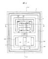
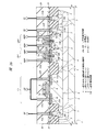
図1、図3、図6および図11は、本実施の形態1の半導体装置の製造工程中のメモリセル領域の要部平面図であり、図2、図4、図5、図7〜図10、図12および図13は、本実施の形態1の半導体装置の製造工程を説明する要部断面図である。また、各断面図において、符号A、A’を付した部分は対応する平面図中のA−A’線に沿った断面、符号B、B’を付した部分は対応する平面図のB−B’線に沿った断面、符号C、C’を付した部分は周辺回路領域の一部(nチャネル型MISFET(Metal Insulator Semiconductor Field Effect Transistor)が形成される領域)の断面を示している。各平面図には、不揮発性メモリセルを構成する主要な導電層とそれらの接続領域のみを示し、導電層間に形成される絶縁膜などの図示は原則として省略する。周辺回路を構成するnチャネル型MISFETなどによってXデコーダ回路、Yデコーダ回路、センスアンプ回路、入出力回路、論理回路などが形成されるが、これらに限らず、マイクロプロセッサ、CPUなどの論理回路を形成してもよい。 1, FIG. 3, FIG. 6 and FIG. 11 are main part plan views of the memory cell region during the manufacturing process of the semiconductor device of the first embodiment, and FIG. 2, FIG. 4, FIG. 10, FIG. 12 and FIG. 13 are cross-sectional views of relevant parts for explaining the manufacturing steps of the semiconductor device of the first embodiment. Further, in each cross-sectional view, the portions denoted by reference symbols A and A ′ are the cross-sections along the line AA ′ in the corresponding plan view, and the portions denoted by reference characters B and B ′ are B- in the corresponding plan view. The cross section along the line B ′ and the portions denoted by reference characters C and C ′ indicate a cross section of a part of the peripheral circuit region (region where an n-channel MISFET (Metal Insulator Semiconductor Field Effect Transistor) is formed). In each plan view, only main conductive layers constituting the nonvolatile memory cell and their connection regions are shown, and an insulating film formed between the conductive layers is not shown in principle. An n-decoder MISFET or the like that constitutes a peripheral circuit forms an X decoder circuit, a Y decoder circuit, a sense amplifier circuit, an input / output circuit, a logic circuit, and the like. It may be formed.
まず、図1および図2に示すように、たとえばp型の単結晶シリコンからなる半導体基板(以下、単に基板と記す)1の主面の素子分離領域に素子分離溝2を形成する。素子分離溝2を形成するには、たとえば基板1の主面をドライエッチングして溝を形成し、続いてこの溝の内部を含む基板1上にCVD(Chemical Vapor Deposition)法で酸化シリコン膜などの絶縁膜を堆積した後、溝の外部の不要な絶縁膜を化学的機械研磨(Chemical Mechanical Polishing;CMP)法で研磨、除去することによって、溝の内部に絶縁膜を残す。この素子分離溝2を形成することにより、メモリアレイの基板1の主面には、素子分離溝2によって周囲を規定された活性領域が形成される。
First, as shown in FIGS. 1 and 2,
次に、たとえば基板1の一部にn型(第1導電型)の不純物(たとえばP(リン)またはAs(ヒ素))をイオン注入した後、基板1に熱処理を施すことによって不純物を基板1中に拡散させることにより、n型半導体分離領域(半導体分離層)3を形成する。
Next, for example, after an n-type (first conductivity type) impurity (for example, P (phosphorus) or As (arsenic)) is ion-implanted into a part of the
続いて、たとえば基板1の一部にn型の不純物(たとえばP)をイオン注入し、他の一部にp型(第2導電型)の不純物(たとえばB(ホウ素))をイオン注入した後、基板1を熱処理してこれらの不純物を基板1中に拡散させることにより、基板1の主面にp型ウエル(第1ウエル、第2ウエル)4およびn型ウエル(第3ウエル)5を形成する。
Subsequently, for example, an n-type impurity (for example, P) is ion-implanted into a part of the
次に、図3および図4に示すように、基板1を熱酸化してp型ウエル4およびn型ウエル5のそれぞれの表面に、たとえば酸化シリコンからなる膜厚13.5nm程度のゲート絶縁膜(第1ゲート絶縁膜)6を形成する。続いて、たとえばCVD法でゲート絶縁膜6上に多結晶シリコン膜を形成した後、その多結晶シリコン膜の上部に、たとえばCVD法で酸化シリコン膜等からなる絶縁膜を堆積する。また、その絶縁膜を形成する前には、多結晶シリコン膜にはn型の導電型を示す不純物が注入されている。続いて、フォトリソグラフィ技術によりパターニングされたフォトレジスト膜(図示は省略)をマスクとしたドライエッチングにより、周辺回路領域の絶縁膜を除去する。続いて、基板1上に、たとえばCVD法で膜厚10nm程度以上の酸化シリコン膜等からなる絶縁膜を堆積する。
Next, as shown in FIGS. 3 and 4, the
次に、フォトリソグラフィ技術によりパターニングされたフォトレジスト膜(図示は省略)をマスクとしたドライエッチングにより、基板1上の絶縁膜をパターニングする。続いて、残った絶縁膜をマスクにしたドライエッチングにより多結晶シリコン膜をパターニングし、ゲート電極(第1ゲート電極)7A、7B、7Cを形成する。ゲート電極7A、7B、7C上の絶縁膜は、キャップ絶縁膜8となる。
Next, the insulating film on the
次に、p型ウエル4とn型ウエル5の一部とにn型の不純物としてPまたはAsをイオン注入することによって低濃度n型半導体領域NMa、NMb、NMcを形成し、p型ウエル4の一部にp型の不純物としてホウ素をイオン注入することによって低濃度p型半導体領域PMa、PMbを形成する。これら低濃度n型半導体領域NMa、NMb、NMcおよび低濃度p型半導体領域PMa、PMbは、後述するn型半導体領域14A、14B、14Cおよびp型半導体領域15A、15Bよりも不純物濃度の低い領域である。
Next, P or As is ion-implanted as an n-type impurity into the p-
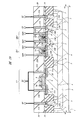
続いて、図5に示すように、基板1上にCVD法で酸化シリコン膜を堆積した後、その酸化シリコン膜およびキャップ絶縁膜8を異方的にエッチングすることにより、ゲート電極7A、7B、7C、およびキャップ絶縁膜9の側壁にサイドウォールスペーサ12を形成する。この時、酸化シリコン膜をサイドウォールスペーサ12へと形成する際に、周辺回路領域のキャップ膜8は除去され、ゲート電極7Cの表面が露出する。これは、メモリセル領域のキャップ絶縁膜8の膜厚が周辺回路領域のキャップ膜8の膜厚に比べて厚くなっているからであり、周辺回路領域のゲート電極7Cの表面が露出したところでエッチングを停止しているからである。
Subsequently, as shown in FIG. 5, after depositing a silicon oxide film on the
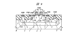
次に、図6および図7に示すように、p型ウエル4とn型ウエル5の一部とにn型の不純物としてPまたはAsをイオン注入することによってn型半導体領域14A、14B、14Cを形成し、p型ウエル4の一部にp型の不純物としてホウ素をイオン注入することによってp型半導体領域15A、15Bを形成する。なお、図6以降の図面(図8〜図10を除く)では説明の簡略化のため、低濃度n型半導体領域NMa、NMb、NMcおよび低濃度p型半導体領域PMa、PMbの記載は省略し、後述する高濃度n型半導体領域14A、14B、14Cおよび高濃度p型半導体領域15A、15Bを代表して図示する。ここまでの工程により、メモリセル領域には、n型半導体領域14Bをソース、ドレインとするデータ書き込み用および消去用のMISFETQw1、Qw2と、n型半導体領域14Bをソース、ドレインとするデータ読出し用のMISFETQr1、Qr2と、ゲート電極7A、7Bおよびp型ウエル4を容量電極としゲート絶縁膜6を容量絶縁膜とする容量素子C1、C2が形成され、周辺回路領域には、n型半導体領域14Cをソース、ドレインとするnチャネル型MISFET(第1MISFET)が形成される。また、メモリセル領域においては、ゲート電極7A、7Bを浮遊ゲートとし、p型半導体領域15Aをコントロールゲートとする不揮発性記憶素子が形成される。
Next, as shown in FIGS. 6 and 7, n-type semiconductor regions 14 </ b> A, 14 </ b> B, 14 </ b> C are formed by ion-implanting P or As as n-type impurities into the p-
ここで、図7の拡大図を図8〜図10にそれぞれ示す。 Here, enlarged views of FIG. 7 are shown in FIGS.
図8に示すように、不揮発性記憶素子のコントロールゲートとなる領域は、低濃度p型半導体領域PMaと高濃度p型半導体領域15Aとを形成するためのイオン注入が施された領域である。また、p型ウェル4の給電部は、低濃度p型半導体領域PMaと高濃度p型半導体領域15Bとを形成するためのイオン注入が施された領域である。同様に、n型ウェル5の給電部は、低濃度n型半導体領域NMaと高濃度n型半導体領域14Aとを形成するためのイオン注入が施された領域である。
As shown in FIG. 8, the region that becomes the control gate of the nonvolatile memory element is a region that has been subjected to ion implantation for forming the low-concentration p-type semiconductor region PMa and the high-concentration p-
図9に示すように、データ書き込み用および消去用のMISFETQw1、Qw2およびデータ読出し用のMISFETQr1、Qr2のソース・ドレイン領域は、それぞれ、低濃度n型半導体領域NMbおよび高濃度のn型半導体領域14Bによって構成されている。また、p型ウェル4の給電部およびn型ウェル5の給電部の説明については、前述の図8と同様である。
As shown in FIG. 9, the source / drain regions of MISFETs Qw1 and Qw2 for data writing and erasing and MISFETs Qr1 and Qr2 for data reading are respectively a low concentration n-type semiconductor region NMb and a high concentration n-
図10に示すように、周辺回路領域のnチャネル型MISFETのソース・ドレイン領域は、それぞれ、低濃度n型半導体領域NMbおよび高濃度のn型半導体領域14Bによって構成されている。
As shown in FIG. 10, the source / drain regions of the n-channel type MISFET in the peripheral circuit region are constituted by a low-concentration n-type semiconductor region NMb and a high-concentration n-
ここで、データ書き込み用および消去用のMISFETQw1、Qw2の低濃度n型半導体領域NMbについては、他の領域の低濃度n型半導体領域NMa、NMcよりも高い不純物濃度で形成することもできる。このようにして低濃度n型半導体領域NMbを形成した場合、MISFETQw1、Qw2の書き込み動作時に発生させるホットエレクトロンの発生量を高くすることが可能となるため、メモリセルの書き込み動作を高速化することができる。 Here, the low concentration n-type semiconductor regions NMb of the MISFETs Qw1 and Qw2 for data writing and erasing can be formed with a higher impurity concentration than the low concentration n-type semiconductor regions NMa and NMc of other regions. When the low-concentration n-type semiconductor region NMb is formed in this way, the amount of hot electrons generated during the write operation of the MISFETs Qw1 and Qw2 can be increased, so that the write operation of the memory cell can be speeded up. Can do.
このように、図8〜図10には、低濃度n型半導体領域NMa、NMb、NMcについて詳細に示したが、他の図面(図7等)においては、説明の簡略化のためその記載を省略し、n型半導体領域14A、14B、14Cおよびp型半導体領域15A、15Bのみを記載している。
As described above, FIGS. 8 to 10 show the low-concentration n-type semiconductor regions NMa, NMb, and NMc in detail, but in other drawings (FIG. 7 and the like), the description is made for the sake of simplicity of explanation. Only the n-
次に、シリサイド層18を形成する。このシリサイド層18の形成については、まず、たとえば基板1上にスパッタリング法でCo(コバルト)膜を堆積する。続いて、基板1を熱処理してCo膜と周辺回路領域のゲート電極7Cとの界面、およびCo膜と基板1との界面にシリサイド反応を生じさせた後、未反応のCo膜をエッチングで除去する。これにより、ゲート電極7Cの表面とソース、ドレイン(n型半導体領域14)の表面とにシリサイド(CoSi2)層18が形成される。また、メモリセル領域においては、n型半導体領域14の表面にシリサイド層18が形成される。ここで、ゲート電極7A、7Bの表面にはキャップ絶縁膜8が残されているため、シリサイド層18は形成されていない。なお、本実施の形態1ではシリサイド層18の材料としてCo(コバルト)を例示したが、これに限られるものではなく、Ti(チタン)、W(タングステン)またはNi(ニッケル)等を使用することもできる。
Next, the
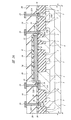
次に、図11および図12に示すように、基板1上にプラズマCVD法で窒化シリコン膜19をゲート電極7A、7B、7C、キャップ絶縁膜8およびサイドウォールスペーサ12を覆うように堆積する。この窒化シリコン膜19は、後の工程で基板1上に層間絶縁膜を形成し、その層間絶縁膜にn型半導体領域14A、14B、14Cおよびp型半導体領域15A、15Bのそれぞれに達するコンタクトホールを形成する際に、素子分離溝に埋め込んだ酸化シリコン膜とのエッチング選択比を大きくすることにより、合わせずれによりコンタクトホールが素子分離溝上に形成されたとしても、コンタクトホールが基板に達してしまうのを防ぐように機能する。また、オーバーエッチングによってシリサイド層18の表面が削れることを防止する機能も有する。すなわち、窒化シリコン膜19はエッチングストッパ膜として機能する。
Next, as shown in FIGS. 11 and 12, a
次に、基板1上に、たとえばCVD法で酸化シリコン膜20を堆積し、続いて化学的機械研磨法で酸化シリコン膜20の表面を平坦化する。続いて、フォトレジスト膜をマスクにして上記酸化シリコン膜20および窒化シリコン膜19をドライエッチングすることにより、n型半導体領域14A、14B、14Cおよびp型半導体領域15A、15Bのそれぞれに達するコンタクトホールを形成する。この時、窒化シリコン膜19は酸化シリコン膜20をエッチングする際のエッチングストッパ膜として機能する。続いて、そのコンタクトホールの内部にプラグ22A〜22Eを形成する。プラグ22Aはn型半導体領域14A上のシリサイド層18に達し、プラグ22Bはn型半導体領域14B上のシリサイド層18に達し、プラグ22Cはn型半導体領域14C上のシリサイド層18に達し、プラグ22Dはp型半導体領域15A上のシリサイド層18に達し、プラグ22Eはp型半導体領域15B上のシリサイド層18に達する。プラグ22A〜22Eを形成するには、たとえばコンタクトホールの内部を含む酸化シリコン膜20上にスパッタリング法でTi(チタン)膜およびTiN(窒化チタン)膜を堆積し、続いてCVD法でTiN膜および金属膜としてW(タングステン)膜を堆積した後、コンタクトホールの外部のW膜、TiN膜およびTi膜を化学的機械研磨法によって除去する。
Next, a
上記の本実施の形態1の半導体装置の製造方法によれば、相補型MISFETを形成する製造工程に他の工程を追加することなく不揮発性メモリを形成することができる。 According to the semiconductor device manufacturing method of the first embodiment described above, the nonvolatile memory can be formed without adding another process to the manufacturing process for forming the complementary MISFET.
次に、図13に示すように、酸化シリコン膜20およびプラグ22A〜22E上に複数の配線23を形成する。配線23を形成するには、たとえば酸化シリコン膜20上にTi膜、Al(アルミニウム)合金膜およびTiN膜をスパッタリング法により順次堆積し、続いてフォトレジスト膜をマスクとしたドライエッチングによりそのTi膜、Al合金膜およびTiN膜をパターニングする。この後、酸化シリコン膜20および配線23を形成した工程と同様の工程を繰り返すことによって、さらに多層に配線層を形成してもよい。
Next, as shown in FIG. 13, a plurality of
次に、本実施の形態1の不揮発性メモリにおけるデータの書き込み、消去および読み出しの各動作について図14〜図17を用いて説明する。図14はメモリセル領域の要部平面図であり、図15〜図17は図14中のD−D’線に沿った断面を示している。なお、図14〜図17中では、説明をわかりやすくするために配線23の図示は省略している。
Next, data writing, erasing, and reading operations in the nonvolatile memory according to the first embodiment will be described with reference to FIGS. FIG. 14 is a plan view of the main part of the memory cell region, and FIGS. 15 to 17 show cross sections taken along the line D-D 'in FIG. In FIG. 14 to FIG. 17, the
まず、図15に示すように、データの書き込み時には、たとえばn型ウエル5(n型半導体分離領域3)に9Vを印加し、p型半導体領域15B(MISFETQw1、Qw2、Qr1、Qr2が形成されたp型ウエル4)に0Vを印加し、p型半導体領域15A(容量素子C1、C2が形成されたp型ウエル4)に順方向の9V(第1電圧)を印加し、データ書き込み用および消去用のMISFETQw1、Qw2のソース、ドレイン(n型半導体領域14B)の一方に7V(第2電圧)を印加し、他方に0Vを印加し、データ読み出し用のMISFETQr1、Qr2のソース、ドレイン(n型半導体領域14B)を開放電位とする。これにより、データ書き込み用および消去用のMISFETQw1、Qw2において、チャネルホットエレクトロン(e-)がゲート電極7Aに注入され、データの書き込みが行われる。
First, as shown in FIG. 15, when data is written, for example, 9V is applied to the n-type well 5 (n-type semiconductor isolation region 3), and p-
データの消去時には、図16に示すように、たとえばn型ウエル5(n型半導体分離領域3)に9Vを印加し、p型半導体領域15B(MISFETQw1、Qw2、Qr1、Qr2が形成されたp型ウエル4)に9Vを印加し、p型半導体領域15A(容量素子C1、C2が形成されたp型ウエル4)に逆方向の−9V(第1電圧)を印加し、データ書き込み用および消去用のMISFETQw1、Qw2およびデータ読み出し用のMISFETQr1、Qr2のソース、ドレイン(n型半導体領域14B)を開放電位とする。ここで、容量素子C1、C2の容量電極(ゲート電極7A、7B)の面積は、MISFETQw1、Qw2のゲート容量を形成する容量電極(ゲート電極7A、7B)の面積より大きいことから(図14参照)、容量素子C1、C2の容量は、MISFETQw1、Qw2のゲート容量(ゲート電極7A、7BとMISFETQw1、Qw2のチャネルとの間で形成される)に比べて大きくなる。そのため、MISFETQw1、Qw2のゲート容量に印加される電圧は、容量素子C1、C2に印加される電圧より大きくなる。これにより、データ書き込み用および消去用のMISFETQw1、Qw2およびデータ読み出し用のMISFETQr1、Qr2において、ゲート電極7Aから電子(e-)をFNトンネル方式でp型ウエル4へ放出する。その結果、たとえばドレイン(n型半導体領域14B)の端部に電界が集中することに起因する素子の劣化を防ぐことができる。素子の劣化を防ぐことにより、電荷のリークを防ぐことが可能となるので、不揮発性メモリのデータ保持特性の劣化を防ぐことが可能となる。また、容量素子C1、C2が形成されたp型ウエル4に負(逆方向)の電圧を印加し、MISFETQw1、Qw2、Qr1、Qr2が形成されたp型ウエル4に正(順方向)の電圧を印加することにより、ゲート破壊を起こさない電圧(9V以下)でデータ消去動作に必要な電位差(18V)を確保することが可能となる。
At the time of erasing data, as shown in FIG. 16, for example, 9V is applied to the n-type well 5 (n-type semiconductor isolation region 3), and the p-
データの読み出し時には、図17に示すように、たとえばn型ウエル5(n型半導体分離領域3)に3Vを印加し、p型半導体領域15B(MISFETQw1、Qw2、Qr1、Qr2が形成されたp型ウエル4)に0Vを印加し、p型半導体領域15A(容量素子C1、C2が形成されたp型ウエル4)に3Vを印加し、データ書き込み用および消去用のMISFETQw1、Qw2のソース、ドレイン(n型半導体領域14B)を開放電位とし、データ読み出し用のMISFETQr1、Qr2のソース、ドレイン(n型半導体領域14B)の一方に1Vを印加し、他方に0Vを印加する。これにより、データ読み出し用のMISFETQr1、Qr2をオンとする。
At the time of reading data, as shown in FIG. 17, for example, 3V is applied to the n-type well 5 (n-type semiconductor isolation region 3), and the p-
ところで、上記の本実施の形態1では、データ書き込み用および消去用のMISFET(Qw1、Qw2)と、データ読出し用のMISFET(Qr1、Qr2)とをそれぞれ形成する場合について例示したが、どちらか一方を省略して、データ書き込み、データ消去およびデータ読み出しのすべての動作を一つのMISFETによって行ってもよい。 In the first embodiment described above, the case where the MISFETs for data writing and erasing (Qw1, Qw2) and the MISFETs for data reading (Qr1, Qr2) are respectively formed is illustrated. May be omitted, and all operations of data writing, data erasing, and data reading may be performed by one MISFET.
上記のような本実施の形態1の不揮発性メモリは、たとえばLCD(Liquid Crystal Display)ドライバにおける電圧制御情報(画質調整用データ)を蓄積させ、ヒューズ回路として用いることができる。この場合、必要に応じてデータの書き換えを行えるので、メモリ容量が書き換え回数分だけ必要となるOTPROM型のヒューズ回路に比べてモジュールサイズを小型化することができる。また、モジュールサイズの小型化により、モジュールの製造コストを低減することができる。 The nonvolatile memory according to the first embodiment as described above can store voltage control information (image quality adjustment data) in, for example, an LCD (Liquid Crystal Display) driver and can be used as a fuse circuit. In this case, since data can be rewritten as necessary, the module size can be reduced as compared with an OTPROM type fuse circuit that requires a memory capacity corresponding to the number of times of rewriting. Further, the module manufacturing cost can be reduced by reducing the module size.
また、上記の本実施の形態1の不揮発性メモリの他の用途として、冗長構成によるDRAM(Dynamic Random Access Memory)の不良メモリセルの救済を例示することができる。この時、メモリセルは単位情報セルとなり、この単位情報セルが複数個集まり、複数個の単位情報セルの不揮発性記憶素子に対する電気的なプログラム回路が形成され、複数個の単位情報セルが被救済回路に対する救済情報の記憶回路となる。これにより、不良救済の信頼性を高くすることができる。 Further, as another application of the above-described nonvolatile memory according to the first embodiment, remedy of defective memory cells of a DRAM (Dynamic Random Access Memory) by a redundant configuration can be exemplified. At this time, the memory cell becomes a unit information cell, and a plurality of the unit information cells are gathered to form an electrical program circuit for the nonvolatile memory element of the plurality of unit information cells, and the plurality of unit information cells are repaired. It becomes a memory circuit for saving information for the circuit. Thereby, the reliability of defect relief can be increased.
また、上記被救済回路に対する別の救済情報記憶回路として、ヒューズ素子の溶断状態に応じて救済情報を記憶するヒューズプログラム回路を更に設けてもよい。ウエハ段階で検出された不良に対する救済をヒューズプログラム回路で行い、バーンイン後に検出された不良に対して上記の電気的なプログラム回路を用いる事により、救済効率を上げることができる。 Further, as another repair information storage circuit for the circuit to be repaired, a fuse program circuit for storing repair information according to the blown state of the fuse element may be further provided. Rescue of defects detected at the wafer stage is performed by a fuse program circuit, and the above-described electrical program circuit is used for defects detected after burn-in, thereby improving the repair efficiency.
また、上記被救済回路は、マイクロコンピュータ内蔵DRAMのメモリセルまたはマイクロコンピュータ内蔵SRAMのメモリセルであってもよい。また、LCDドライバの救済回路を構成することも可能である。 The circuit to be relieved may be a DRAM built-in DRAM memory cell or a microcomputer built-in SRAM memory cell. It is also possible to configure a relief circuit for the LCD driver.
(実施の形態2)
次に、本実施の形態2の不揮発性メモリにおけるデータの書き込み、消去および読み出しの各動作について図18を用いて説明する。
(Embodiment 2)
Next, data writing, erasing, and reading operations in the nonvolatile memory according to the second embodiment will be described with reference to FIG.
図18は、前記実施の形態1における図14中のD−D’線に沿った断面を示したものである。図18に示すように、本実施の形態2の不揮発性メモリの構造は、前記実施の形態1の不揮発性メモリとほぼ同様である。 FIG. 18 shows a cross section taken along line D-D ′ in FIG. 14 in the first embodiment. As shown in FIG. 18, the structure of the nonvolatile memory according to the second embodiment is substantially the same as that of the nonvolatile memory according to the first embodiment.
本実施の形態2の不揮発性メモリにおけるデータの書き込み動作および読み出し動作は、前記実施の形態1の不揮発性メモリと同様である。図18に示すように、データの消去時には、たとえばn型ウエル5(n型半導体分離領域3)に9Vを印加し、p型半導体領域15B(MISFETQw1、Qw2、Qr1、Qr2が形成されたp型ウエル4)にOVを印加し、p型半導体領域15A(容量素子C1、C2が形成されたp型ウエル4)に−9Vを印加し、データ書き込み用および消去用のMISFETQw1、Qw2のドレイン(n型半導体領域14B)に7Vを印加し、ソース(n型半導体領域14B)を開放電位とし、データ読み出し用のMISFETQr1、Qr2のソース、ドレイン(n型半導体領域14B)を開放電位とする。この時、データ書き込み用および消去用のMISFETQw1、Qw2においては、ゲート電極7Aの端部に電界が集中することから、前記実施の形態1におけるデータ消去動作時の電圧(9V)より低い電圧(7V)でもゲート電極7Aから電子(e-)を放出することができる。これにより、データ書き込み用および消去用のMISFETQw1、Qw2において、ゲート電極7Aの端部からデータ書き込み用および消去用のMISFETQw1、Qw2のドレイン(n型半導体領域14B)へ電子(e-)を放出する。
Data write and read operations in the nonvolatile memory of the second embodiment are the same as those of the nonvolatile memory of the first embodiment. As shown in FIG. 18, when erasing data, for example, 9V is applied to the n-type well 5 (n-type semiconductor isolation region 3), and the p-
また、データ書き込み用および消去用のMISFETQw1、Qw2においては、ゲート電極7Aの端部に電界が集中することから、データ書き込み用および消去用のMISFETQw1、Qw2の素子劣化が起こらないように、ゲート絶縁膜6については、電界集中に耐え得るのに十分な膜厚(たとえば13.5nm程度)で形成しておく。
In the MISFETs Qw1 and Qw2 for data writing and erasing, since the electric field is concentrated on the end portion of the
上記のような本実施の形態2によっても、前記実施の形態1と同様の効果を得ることができる。 According to the second embodiment as described above, the same effect as in the first embodiment can be obtained.
(実施の形態3)
次に、本実施の形態3の不揮発性メモリにおけるデータの書き込み、消去および読み出しの各動作について図19を用いて説明する。
(Embodiment 3)
Next, data writing, erasing, and reading operations in the nonvolatile memory of
図19は、前記実施の形態1における図14中のD−D’線に沿った断面を示したものである。図19に示すように、本実施の形態3の不揮発性メモリの構造は、前記実施の形態1の不揮発性メモリとほぼ同様である。 FIG. 19 shows a cross section taken along line D-D ′ in FIG. 14 in the first embodiment. As shown in FIG. 19, the structure of the nonvolatile memory according to the third embodiment is substantially the same as that of the nonvolatile memory according to the first embodiment.
本実施の形態3の不揮発性メモリにおけるデータの消去動作および読み出し動作は、前記実施の形態1の不揮発性メモリと同様である。図19に示すように、データの書き込み時には、たとえばn型ウエル5(n型半導体分離領域3)に9Vを印加し、p型半導体領域15B(MISFETQw1、Qw2、Qr1、Qr2が形成されたp型ウエル4)に−9Vを印加し、p型半導体領域15A(容量素子C1、C2が形成されたp型ウエル4)に9Vを印加し、データ書き込み用および消去用のMISFETQw1、Qw2およびデータ読み出し用のMISFETQr1、Qr2のソース、ドレイン(n型半導体領域14B)を開放電位とする。これにより、データ書き込み用および消去用のMISFETQw1、Qw2およびデータ読み出し用のMISFETQr1、Qr2において、チャネル全面でFNトンネル方式によって電子(e-)がゲート電極7Aに注入され、データの書き込みが行われる。
The data erasing operation and reading operation in the nonvolatile memory of the third embodiment are the same as those of the nonvolatile memory of the first embodiment. As shown in FIG. 19, at the time of data writing, for example, 9V is applied to the n-type well 5 (n-type semiconductor isolation region 3), and the p-
上記のような本実施の形態3によっても、前記実施の形態1と同様の効果を得ることができる。 According to the third embodiment as described above, the same effect as in the first embodiment can be obtained.
(実施の形態4)
図20は、本実施の形態4の半導体装置のメモリセル部の要部断面図であり、前記実施の形態1において示した各平面図中のA−A’線に相当する断面を示したものである。
(Embodiment 4)
FIG. 20 is a fragmentary cross-sectional view of the memory cell portion of the semiconductor device according to the fourth embodiment, showing a cross section corresponding to the line AA ′ in each plan view shown in the first embodiment. It is.
半導体素子や配線の微細加工によって、p型ウエル4とn型ウエル5との間の接合耐圧が十分に得られなくなってしまった場合には、図20に示すように、p型ウエル4とn型ウエル5とを離間して形成してもよい。それにより、p型ウエル4とn型ウエル5との間の接合耐圧を向上することができる。また、2つのp型ウエル4の間が十分に広い場合には、n型ウエル5は省略してもよい。
If a sufficient junction breakdown voltage between the p-
上記のような本実施の形態4によっても、前記実施の形態1と同様の効果を得ることができる。 According to the fourth embodiment as described above, the same effect as in the first embodiment can be obtained.
(実施の形態5)
次に、本実施の形態5の不揮発性メモリにおけるデータの消去動作について説明する。
(Embodiment 5)
Next, a data erasing operation in the nonvolatile memory according to the fifth embodiment will be described.
図21は、前記実施の形態1における図14中のD−D’線に沿った断面を示したものである。図21に示すように、本実施の形態5の不揮発性メモリの構造は、前記実施の形態1の不揮発性メモリとほぼ同様である。 FIG. 21 shows a cross section taken along line D-D ′ in FIG. 14 in the first embodiment. As shown in FIG. 21, the structure of the nonvolatile memory according to the fifth embodiment is almost the same as that of the nonvolatile memory according to the first embodiment.
本実施の形態5の不揮発性メモリにおけるデータの消去時には、たとえばn型ウエル5(n型半導体分離領域3)に9Vを印加し、p型半導体領域15B(MISFETQw1、Qw2、Qr1、Qr2が形成されたp型ウエル4)に9Vを印加し、p型半導体領域15A(容量素子C1、C2が形成されたp型ウエル4)に−9Vを印加し、データ書き込み用および消去用のMISFETQw1、Qw2のソース、ドレインおよびデータ読み出し用のMISFETQr1、Qr2のソース、ドレイン(n型半導体領域14B)に9Vを印加する。前記の実施の形態1のように、データ消去時にデータ書き込み用および消去用のMISFETQw1、Qw2のドレインを開放電位とするためには、他に制御用のMISFETが必要となり、半導体装置の小型化を阻害してしまうことになる。そこで、本実施の形態5では、データ書き込み用および消去用のMISFETQw1、Qw2とデータ読み出し用のMISFETQr1、Qr2のソース、ドレインに9Vを印加することにより、前記実施の形態1と同様の動作状況とすることができる。
When erasing data in the nonvolatile memory according to the fifth embodiment, for example, 9V is applied to the n-type well 5 (n-type semiconductor isolation region 3), and p-
ここで、データ書き込み用および消去用のMISFETQw1、Qw2のチャネル領域では、ホットエレクトロンを発生しやすくするために不純物濃度が高くなっており、接合耐圧が前記実施の形態1で説明したゲート破壊を起こさない電圧(9V以下)よりも低く、約7V以下となっている。そこで、図22示すように、p型ウエル4に電圧9Vが印加されるのに先立ってMISFETQw1、Qw2のドレインに9Vを印加する。また、MISFETQw1、Qw2のドレイン電圧を0Vに戻すのに先立ってp型ウエル4の電圧を0Vに戻すと、双方の電位差V1が上記接合耐圧を超えてしまい接合破壊を引き起こしてしまう。そこで、本実施の形態5では、データ消去動作時においては、図23および図24に示すようなタイミングでMISFETQw1、Qw2、Qr1、Qr2が形成されたp型ウエル4およびデータ書き込み用および消去用のMISFETQw1、Qw2のドレイン(n型半導体領域14B)に電圧を印加し、双方の電位差が約7V以上とならないようにすることを例示する。
Here, in the channel regions of the MISFETs Qw1 and Qw2 for data writing and erasing, the impurity concentration is high in order to facilitate the generation of hot electrons, and the junction breakdown voltage causes the gate breakdown described in the first embodiment. The voltage is lower than the voltage (9 V or less) and about 7 V or less. Therefore, as shown in FIG. 22, before the
たとえば、図23に示すように、p型ウエル4の電圧を立ち上げるのに先立ってMISFETQw1、Qw2のドレインの電圧を立ち上げる。この時、双方の電圧は、急峻に立ち上げずに緩やかに上昇させ、双方の電位差V1が上記接合耐圧を超えない約7V以上とならないようにする。また、MISFETQw1、Qw2のドレイン電圧を0Vに戻すのに先立ってp型ウエル4の電圧を0Vに戻し、この時の双方の電圧変化も急峻とならないようにすることにより、双方の電位差V1が上記接合耐圧を超えない約7V以上とならないようにすることができる。
For example, as shown in FIG. 23, the voltage of the drains of the MISFETs Qw1 and Qw2 is raised prior to raising the voltage of the p-
また、図24に示すように、p型ウエル4の電圧を立ち上げるのに先立ってMISFETQw1、Qw2のドレインの電圧を立ち上げ、9Vまで上昇させる前に4Vもしくは5Vとし、その間にp型ウエル4の電圧を立ち上げてもよい。この時、p型ウエル4の電圧は、タイミングが異なるだけでMISFETQw1、Qw2のドレインの電圧と同様に変化させる。それにより、双方の電位差V1が上記接合耐圧を超えない約7V以上とならないようにすることができる。また、MISFETQw1、Qw2のドレイン電圧およびp型ウエル4の電圧を0Vに戻す際には、MISFETQw1、Qw2のドレイン電圧を低下させるのに先立ってp型ウエル4の電圧を低下させ、その際の電圧変化は、電圧を上昇させる際の変化過程を逆に経るようにすればよい。
Further, as shown in FIG. 24, before raising the voltage of the p-
上記のような本実施の形態5によっても、前記実施の形態1と同様の効果を得ることができる。 According to the fifth embodiment as described above, the same effect as in the first embodiment can be obtained.
以上、本発明者によってなされた発明を実施の形態に基づき具体的に説明したが、本発明は前記実施の形態に限定されるものではなく、その要旨を逸脱しない範囲で種々変更可能であることはいうまでもない。 As mentioned above, the invention made by the present inventor has been specifically described based on the embodiment. However, the present invention is not limited to the embodiment, and various modifications can be made without departing from the scope of the invention. Needless to say.
たとえば、前記実施の形態1において、書き込み時に、データ読み出し用MISFETQr1、Qr2のソース、ドレインを0Vにしてもよいし、読み出し時に、データ書き込み用および消去用MISFETQw1、Qw2のソース、ドレインを0Vにしてもよい。また、LCDドライバのように、20V程度以上の高耐圧MISFETを含む半導体装置では、前記実施の形態1において、消去時に、n型ウェル5に0V、p型半導体領域15Bに0V、p型半導体領域15Aに−18Vを印可し、データ書き込み用および消去用MISFETQw1、Qw2およびデータ読み出し用MISFETQr1、Qr2のソース、ドレインを0Vまたは開放電位としてもよい。
For example, in the first embodiment, the source and drain of the data read MISFETs Qr1 and Qr2 may be set to 0 V at the time of writing, and the source and drain of the data write and erase MISFETs Qw1 and Qw2 are set to 0 V at the time of reading. Also good. Further, in a semiconductor device including a high breakdown voltage MISFET of about 20V or more, such as an LCD driver, in the first embodiment, at the time of erasing, 0V is applied to the n-
本発明の半導体装置は、たとえば不揮発性メモリを有する半導体装置に適用することができる。 The semiconductor device of the present invention can be applied to a semiconductor device having a nonvolatile memory, for example.
1 基板
2 素子分離溝
3 n型半導体分離領域(半導体分離層)
4 p型ウエル(第1ウエル、第2ウエル)
5 n型ウエル(第3ウエル)
6 ゲート絶縁膜(第1ゲート絶縁膜)
7A、7B ゲート電極(第1ゲート電極)
7C ゲート電極
8 キャップ絶縁膜
12 サイドウォールスペーサ
14A、14B、14C n型半導体領域
15A、15B p型半導体領域
18 シリサイド層
19 窒化シリコン膜
20 酸化シリコン膜
22A〜22E プラグ
23 配線
C1、C2 容量素子
NMa、NMb、NMc 低濃度n型半導体領域
PMa、PMb 低濃度p型半導体領域
Qr1、Qr2、Qw1、Qw2 MISFET
1
4 p-type well (first well, second well)
5 n-type well (third well)
6 Gate insulation film (first gate insulation film)
7A, 7B Gate electrode (first gate electrode)
Claims (12)
半導体基板の主面に形成された第1導電型の半導体分離層と、
前記半導体分離層中に形成された第2導電型の第1ウエルおよび第2導電型の第2ウエルと、
前記半導体分離層中に形成され、前記第1ウエルと前記第2ウエルとを分離する第1導電型の第3ウエルと、
前記第1ウエル上および前記第2ウエル上に第1ゲート絶縁膜を介して延在する第1ゲート電極と、
前記第1ウエルに形成され、前記第1ゲート電極をゲート電極とするデータ書き込み用MISFETおよびデータ読み出し用MISFETと、
前記第2ウエルに形成され、前記第1ゲート電極を容量電極とする容量素子とを有し、
前記不揮発性メモリセルへのデータ書き込み時には、前記第2ウエルに順方向の第1電圧が印加され、
前記不揮発性メモリセルのデータ消去時には、前記第2ウエルに逆方向の前記第1電圧が印加されることを特徴とする半導体装置。 A semiconductor device including a nonvolatile memory cell,
A first conductivity type semiconductor isolation layer formed on the main surface of the semiconductor substrate;
A second conductivity type first well and a second conductivity type second well formed in the semiconductor isolation layer;
A third well of a first conductivity type formed in the semiconductor isolation layer and separating the first well and the second well;
A first gate electrode extending over the first well and the second well via a first gate insulating film;
A data write MISFET and a data read MISFET formed in the first well and having the first gate electrode as a gate electrode;
A capacitor element formed in the second well and having the first gate electrode as a capacitor electrode;
When writing data to the nonvolatile memory cell, a first voltage in the forward direction is applied to the second well,
The semiconductor device according to claim 1, wherein the first voltage in the reverse direction is applied to the second well when erasing data in the nonvolatile memory cell.
前記半導体分離層中には、複数の前記不揮発性メモリセルが形成されていることを特徴とする半導体装置。 The semiconductor device according to claim 1,
A semiconductor device, wherein a plurality of the nonvolatile memory cells are formed in the semiconductor isolation layer.
前記半導体基板の前記主面上には、前記不揮発性メモリセルには含まれない第1MISFETが形成され、
前記第1MISFETは、前記第1ゲート絶縁膜を含むことを特徴とする半導体装置。 The semiconductor device according to claim 1,
A first MISFET not included in the nonvolatile memory cell is formed on the main surface of the semiconductor substrate.
The semiconductor device according to claim 1, wherein the first MISFET includes the first gate insulating film.
前記第1ゲート絶縁膜は、膜厚が13.5nmであり、
前記第1電圧は、9Vであることを特徴とする半導体装置。 The semiconductor device according to claim 1,
The first gate insulating film has a thickness of 13.5 nm,
The semiconductor device according to claim 1, wherein the first voltage is 9V.
前記不揮発性メモリセルへのデータ書き込み時には、前記データ書き込み用MISFETのドレインに前記第1電圧より低い順方向の第2電圧を印加して、前記データ書き込み用MISFETのチャネルから前記第1ゲート電極にホットエレクトロンを注入し、
前記不揮発性メモリセルのデータ消去時には、前記データ書き込み用MISFETのソースおよび前記ドレインを開放電位とし、前記第1ゲート電極から前記データ書き込み用MISFETのチャネルへ前記ホットエレクトロンを放出することを特徴とする半導体装置。 The semiconductor device according to claim 1,
At the time of data writing to the nonvolatile memory cell, a forward second voltage lower than the first voltage is applied to the drain of the data write MISFET, and the channel of the data write MISFET is applied to the first gate electrode. Injecting hot electrons,
When erasing data in the nonvolatile memory cell, the source and drain of the data write MISFET are set to an open potential, and the hot electrons are discharged from the first gate electrode to the channel of the data write MISFET. Semiconductor device.
前記不揮発性メモリセルへのデータ書き込み時には、前記データ書き込み用MISFETのドレインに前記第1電圧より低い順方向の第2電圧を印加して、前記データ書き込み用MISFETのチャネルから前記第1ゲート電極にホットエレクトロンを注入し、
前記不揮発性メモリセルのデータ消去時には、前記データ書き込み用MISFETのソースを開放電位として前記ドレインに順方向の前記第2電圧を印加し、前記第1ゲート電極から前記ドレインへ前記ホットエレクトロンを放出することを特徴とする半導体装置。 The semiconductor device according to claim 4.
At the time of data writing to the nonvolatile memory cell, a forward second voltage lower than the first voltage is applied to the drain of the data write MISFET, and the channel of the data write MISFET is applied to the first gate electrode. Injecting hot electrons,
When erasing data in the nonvolatile memory cell, the source of the data write MISFET is set to an open potential, the second voltage in the forward direction is applied to the drain, and the hot electrons are discharged from the first gate electrode to the drain. A semiconductor device.
前記不揮発性メモリセルへのデータ書き込み時には、前記データ書き込み用MISFETのソースおよびドレインを開放電位として前記第1ウエルから前記第1ゲート電極にエレクトロンを注入し、
前記不揮発性メモリセルのデータ消去時には、前記データ書き込み用MISFETのソースおよび前記ドレインを開放電位とし、前記第1ゲート電極から前記データ書き込み用MISFETのチャネルへ前記エレクトロンを放出することを特徴とする半導体装置。 The semiconductor device according to claim 1,
At the time of data writing to the nonvolatile memory cell, electrons are injected from the first well to the first gate electrode with the source and drain of the data writing MISFET as open potentials,
When erasing data in the nonvolatile memory cell, the source and drain of the data write MISFET are set to an open potential, and the electrons are discharged from the first gate electrode to the channel of the data write MISFET. apparatus.
前記不揮発性メモリセルには、LCDドライバの電圧制御もしくはRAM救済情報が記録されることを特徴とする半導体装置。 The semiconductor device according to claim 1,
A semiconductor device, wherein voltage control of LCD driver or RAM relief information is recorded in the nonvolatile memory cell.
前記データ書き込み用MISFETおよび前記データ読み出し用MISFETは、1つのMISFETで兼用されることを特徴とする半導体装置。 The semiconductor device according to claim 1,
The data writing MISFET and the data reading MISFET are shared by a single MISFET.
前記第3ウエルは、前記第1ウエルおよび前記第2ウエルと離間して形成されていることを特徴とする半導体装置。 The semiconductor device according to claim 1,
The semiconductor device according to claim 1, wherein the third well is formed apart from the first well and the second well.
前記不揮発性メモリセルのデータ消去時には、前記データ書き込み用MISFETと前記読み出し用MISFETのソース、ドレインに印可する第2電圧と前記第1ウェルに印可する第1電圧の差がドレイン接合耐圧以上にならないように制御することを特徴とする半導体装置。 The semiconductor device according to claim 1,
When erasing data in the nonvolatile memory cell, the difference between the second voltage applied to the source and drain of the data write MISFET and the read MISFET and the first voltage applied to the first well does not exceed the drain junction breakdown voltage. The semiconductor device is controlled as described above.
半導体基板の主面に形成された第1導電型の半導体分離層と、
前記半導体分離層中に形成された第2導電型の第1ウエルおよび第2導電型の第2ウエルと、
前記半導体分離層中にて、前記第1ウエルと離間して形成された第2導電型の第2ウエルと、
前記第1ウエル上および前記第2ウエル上に第1ゲート絶縁膜を介して延在する第1ゲート電極と、
前記第1ウエルに形成され、前記第1ゲート電極をゲート電極とするデータ書き込み用MISFETおよびデータ読み出し用MISFETとを有し、
前記不揮発性メモリセルへのデータ書き込み時には、前記第2ウエルに順方向の第1電圧が印加され、
前記不揮発性メモリセルのデータ消去時には、前記第2ウエルに逆方向の前記第1電圧が印加されることを特徴とする半導体装置。 A semiconductor device including a nonvolatile memory cell,
A first conductivity type semiconductor isolation layer formed on the main surface of the semiconductor substrate;
A second conductivity type first well and a second conductivity type second well formed in the semiconductor isolation layer;
A second well of a second conductivity type formed in the semiconductor isolation layer and spaced apart from the first well;
A first gate electrode extending over the first well and the second well via a first gate insulating film;
A data write MISFET and a data read MISFET formed in the first well and having the first gate electrode as a gate electrode;
When writing data to the nonvolatile memory cell, a first voltage in the forward direction is applied to the second well,
The semiconductor device according to claim 1, wherein the first voltage in the reverse direction is applied to the second well when erasing data in the nonvolatile memory cell.
Priority Applications (6)
| Application Number | Priority Date | Filing Date | Title |
|---|---|---|---|
| JP2004261751A JP4881552B2 (en) | 2004-09-09 | 2004-09-09 | Semiconductor device |
| TW094116894A TWI424532B (en) | 2004-09-09 | 2005-05-24 | A semiconductor device |
| US11/206,968 US7313026B2 (en) | 2004-09-09 | 2005-08-19 | Semiconductor device |
| KR1020050076135A KR101067093B1 (en) | 2004-09-09 | 2005-08-19 | A semiconductor device |
| US11/925,106 US7466599B2 (en) | 2004-09-09 | 2007-10-26 | Semiconductor device |
| US12/270,346 US20090154253A1 (en) | 2004-09-09 | 2008-11-13 | semiconductor device |
Applications Claiming Priority (1)
| Application Number | Priority Date | Filing Date | Title |
|---|---|---|---|
| JP2004261751A JP4881552B2 (en) | 2004-09-09 | 2004-09-09 | Semiconductor device |
Publications (3)
| Publication Number | Publication Date |
|---|---|
| JP2006080247A true JP2006080247A (en) | 2006-03-23 |
| JP2006080247A5 JP2006080247A5 (en) | 2007-10-18 |
| JP4881552B2 JP4881552B2 (en) | 2012-02-22 |
Family
ID=35996040
Family Applications (1)
| Application Number | Title | Priority Date | Filing Date |
|---|---|---|---|
| JP2004261751A Expired - Fee Related JP4881552B2 (en) | 2004-09-09 | 2004-09-09 | Semiconductor device |
Country Status (4)
| Country | Link |
|---|---|
| US (3) | US7313026B2 (en) |
| JP (1) | JP4881552B2 (en) |
| KR (1) | KR101067093B1 (en) |
| TW (1) | TWI424532B (en) |
Cited By (7)
| Publication number | Priority date | Publication date | Assignee | Title |
|---|---|---|---|---|
| JP2007123830A (en) * | 2005-09-29 | 2007-05-17 | Matsushita Electric Ind Co Ltd | Non-volatile semiconductor memory device |
| JP2008270550A (en) * | 2007-04-20 | 2008-11-06 | Interchip Kk | Element for nonvolatile memory, nonvolatile memory, and shift register having built-in nonvolatile memory |
| JP2009151920A (en) * | 2007-12-19 | 2009-07-09 | Powerchip Semiconductor Corp | Integrated circuit with memory device and discharge circuit |
| WO2009139429A1 (en) * | 2008-05-16 | 2009-11-19 | Semiconductor Energy Laboratory Co., Ltd. | Nonvolatile semiconductor memory device and manufacturing method thereof |
| US7623371B2 (en) | 2006-06-22 | 2009-11-24 | Renesas Technology Corp. | Semiconductor device |
| US8975127B2 (en) | 2007-06-11 | 2015-03-10 | Renesas Electronics Corporation | Semiconductor device and method of manufacturing the same |
| KR101540509B1 (en) * | 2007-06-11 | 2015-07-31 | 르네사스 일렉트로닉스 가부시키가이샤 | Semiconductor device and method for manufacturing the same |
Families Citing this family (13)
| Publication number | Priority date | Publication date | Assignee | Title |
|---|---|---|---|---|
| KR100604871B1 (en) * | 2004-06-17 | 2006-07-31 | 삼성전자주식회사 | Complementary non-volatile memory device, methods of operating and manufacturing the same and logic device and semiconductor device comprising the same |
| JP4800109B2 (en) * | 2005-09-13 | 2011-10-26 | ルネサスエレクトロニクス株式会社 | Semiconductor device |
| KR100735753B1 (en) | 2005-10-04 | 2007-07-06 | 삼성전자주식회사 | Flash memory device having a shared bit line and fabrication method thereof |
| US7639536B2 (en) * | 2008-03-07 | 2009-12-29 | United Microelectronics Corp. | Storage unit of single-conductor non-volatile memory cell and method of erasing the same |
| JP2010087357A (en) * | 2008-10-01 | 2010-04-15 | Toshiba Corp | Nonvolatile semiconductor storage device |
| US10046141B2 (en) | 2008-12-30 | 2018-08-14 | Biosense Webster, Inc. | Deflectable sheath introducer |
| KR20110047819A (en) * | 2009-10-30 | 2011-05-09 | 주식회사 하이닉스반도체 | Unit block circuit in a semiconductor device |
| BR112012022478B1 (en) * | 2010-03-10 | 2021-09-21 | Probiodrug Ag | HETEROCYCLIC GLUTAMINYL CYCLASE INHIBITORS (QC, EC 2.3.2.5), THEIR PREPARATION PROCESS, AND PHARMACEUTICAL COMPOSITION |
| US8958245B2 (en) | 2010-06-17 | 2015-02-17 | Ememory Technology Inc. | Logic-based multiple time programming memory cell compatible with generic CMOS processes |
| US9042174B2 (en) | 2010-06-17 | 2015-05-26 | Ememory Technology Inc. | Non-volatile memory cell |
| JP5705053B2 (en) * | 2011-07-26 | 2015-04-22 | ルネサスエレクトロニクス株式会社 | Semiconductor device |
| JP2013102119A (en) * | 2011-11-07 | 2013-05-23 | Ememory Technology Inc | Non-volatile memory cell |
| US9361982B2 (en) * | 2014-02-04 | 2016-06-07 | Stmicroelectronics S.R.L. | Embedded non-volatile memory with single polysilicon layer memory cells programmable through band-to-band tunneling-induced hot electron and erasable through fowler-nordheim tunneling |
Citations (9)
| Publication number | Priority date | Publication date | Assignee | Title |
|---|---|---|---|---|
| JPH10335505A (en) * | 1997-05-09 | 1998-12-18 | Motorola Inc | Single level gate non-volatile memory element and its accessing method |
| JP2000269448A (en) * | 1999-03-12 | 2000-09-29 | Toshiba Corp | Manufacture of semiconductor device |
| JP2001185633A (en) * | 1999-12-15 | 2001-07-06 | Texas Instr Inc <Ti> | Eeprom device |
| JP2001257324A (en) * | 2000-03-09 | 2001-09-21 | Hitachi Ltd | Semiconductor integrated circuit |
| JP2002541669A (en) * | 1999-03-31 | 2002-12-03 | コーニンクレッカ フィリップス エレクトロニクス エヌ ヴィ | Semiconductor device having a non-volatile memory cell |
| WO2003088366A1 (en) * | 2002-04-15 | 2003-10-23 | Stmicroelectronics Sa | Non-volatile, programmable, electrically erasable memory semiconductor device having a single grid material layer and corresponding magnetic core plane |
| JP2003347435A (en) * | 2002-05-24 | 2003-12-05 | Ricoh Co Ltd | Semiconductor device |
| US6788574B1 (en) * | 2001-12-06 | 2004-09-07 | Virage Logic Corporation | Electrically-alterable non-volatile memory cell |
| JP2005533372A (en) * | 2002-07-09 | 2005-11-04 | インピンジ インコーポレイテッド | Floating gate semiconductor structure |
Family Cites Families (9)
| Publication number | Priority date | Publication date | Assignee | Title |
|---|---|---|---|---|
| JP3083547B2 (en) * | 1990-07-12 | 2000-09-04 | 株式会社日立製作所 | Semiconductor integrated circuit device |
| DE4311358C2 (en) * | 1992-04-07 | 1999-07-22 | Mitsubishi Electric Corp | Non-volatile semiconductor memory device and operating method for a non-volatile semiconductor memory device and method for programming information into a non-volatile semiconductor memory device |
| JPH07240473A (en) * | 1994-03-01 | 1995-09-12 | Fujitsu Ltd | Semiconductor memory and its fabrication |
| JP4072300B2 (en) | 1999-12-22 | 2008-04-09 | 日本特殊陶業株式会社 | Wiring board with ceramic laminated structure |
| US6284603B1 (en) * | 2000-07-12 | 2001-09-04 | Chartered Semiconductor Manufacturing Inc. | Flash memory cell structure with improved channel punch-through characteristics |
| JP4923321B2 (en) | 2000-09-12 | 2012-04-25 | ソニー株式会社 | Method of operating nonvolatile semiconductor memory device |
| CN1669155A (en) | 2002-05-09 | 2005-09-14 | 伊皮杰有限公司 | Pseudo-nonvolatile direct-tunneling floating-gate device |
| JP4601287B2 (en) * | 2002-12-26 | 2010-12-22 | ルネサスエレクトロニクス株式会社 | Nonvolatile semiconductor memory device |
| JP2004241558A (en) * | 2003-02-05 | 2004-08-26 | Toshiba Corp | Nonvolatile semiconductor memory and its manufacturing method, and semiconductor integrated circuit and nonvolatile semiconductor memory system |
-
2004
- 2004-09-09 JP JP2004261751A patent/JP4881552B2/en not_active Expired - Fee Related
-
2005
- 2005-05-24 TW TW094116894A patent/TWI424532B/en active
- 2005-08-19 US US11/206,968 patent/US7313026B2/en active Active
- 2005-08-19 KR KR1020050076135A patent/KR101067093B1/en active IP Right Grant
-
2007
- 2007-10-26 US US11/925,106 patent/US7466599B2/en active Active
-
2008
- 2008-11-13 US US12/270,346 patent/US20090154253A1/en not_active Abandoned
Patent Citations (10)
| Publication number | Priority date | Publication date | Assignee | Title |
|---|---|---|---|---|
| JPH10335505A (en) * | 1997-05-09 | 1998-12-18 | Motorola Inc | Single level gate non-volatile memory element and its accessing method |
| JP2000269448A (en) * | 1999-03-12 | 2000-09-29 | Toshiba Corp | Manufacture of semiconductor device |
| JP2002541669A (en) * | 1999-03-31 | 2002-12-03 | コーニンクレッカ フィリップス エレクトロニクス エヌ ヴィ | Semiconductor device having a non-volatile memory cell |
| JP2001185633A (en) * | 1999-12-15 | 2001-07-06 | Texas Instr Inc <Ti> | Eeprom device |
| JP2001257324A (en) * | 2000-03-09 | 2001-09-21 | Hitachi Ltd | Semiconductor integrated circuit |
| US6788574B1 (en) * | 2001-12-06 | 2004-09-07 | Virage Logic Corporation | Electrically-alterable non-volatile memory cell |
| WO2003088366A1 (en) * | 2002-04-15 | 2003-10-23 | Stmicroelectronics Sa | Non-volatile, programmable, electrically erasable memory semiconductor device having a single grid material layer and corresponding magnetic core plane |
| JP2005522884A (en) * | 2002-04-15 | 2005-07-28 | エスティマイクロエレクトロニクス エスエー | Semiconductor memory devices |
| JP2003347435A (en) * | 2002-05-24 | 2003-12-05 | Ricoh Co Ltd | Semiconductor device |
| JP2005533372A (en) * | 2002-07-09 | 2005-11-04 | インピンジ インコーポレイテッド | Floating gate semiconductor structure |
Cited By (16)
| Publication number | Priority date | Publication date | Assignee | Title |
|---|---|---|---|---|
| JP2007123830A (en) * | 2005-09-29 | 2007-05-17 | Matsushita Electric Ind Co Ltd | Non-volatile semiconductor memory device |
| US8351255B2 (en) | 2006-06-22 | 2013-01-08 | Renesas Electronics Corporation | Semiconductor device |
| US8189377B2 (en) | 2006-06-22 | 2012-05-29 | Renesas Electronics Corporation | Semiconductor device |
| US7623371B2 (en) | 2006-06-22 | 2009-11-24 | Renesas Technology Corp. | Semiconductor device |
| US7940561B2 (en) | 2006-06-22 | 2011-05-10 | Renesas Electronics Corporation | Semiconductor device |
| JP2008270550A (en) * | 2007-04-20 | 2008-11-06 | Interchip Kk | Element for nonvolatile memory, nonvolatile memory, and shift register having built-in nonvolatile memory |
| KR101540509B1 (en) * | 2007-06-11 | 2015-07-31 | 르네사스 일렉트로닉스 가부시키가이샤 | Semiconductor device and method for manufacturing the same |
| US8975127B2 (en) | 2007-06-11 | 2015-03-10 | Renesas Electronics Corporation | Semiconductor device and method of manufacturing the same |
| US9184126B2 (en) | 2007-06-11 | 2015-11-10 | Renesas Electronics Corporation | Semiconductor device and method of manufacturing the same |
| US9601433B2 (en) | 2007-06-11 | 2017-03-21 | Renesas Electronics Corporation | Semiconductor device and method of manufacturing the same |
| US9812317B2 (en) | 2007-06-11 | 2017-11-07 | Renesas Electronics Corporation | Semiconductor device and method of manufacturing the same |
| US10096467B2 (en) | 2007-06-11 | 2018-10-09 | Renesas Electronics Corporation | Semiconductor device and method of manufacturing the same |
| JP2009151920A (en) * | 2007-12-19 | 2009-07-09 | Powerchip Semiconductor Corp | Integrated circuit with memory device and discharge circuit |
| US8872251B2 (en) | 2008-05-16 | 2014-10-28 | Semiconductor Energy Laboratory Co., Ltd. | Nonvolatile semiconductor memory device and manufacturing method thereof |
| US8188535B2 (en) | 2008-05-16 | 2012-05-29 | Semiconductor Energy Laboratory Co., Ltd. | Nonvolatile semiconductor memory device and manufacturing method thereof |
| WO2009139429A1 (en) * | 2008-05-16 | 2009-11-19 | Semiconductor Energy Laboratory Co., Ltd. | Nonvolatile semiconductor memory device and manufacturing method thereof |
Also Published As
| Publication number | Publication date |
|---|---|
| JP4881552B2 (en) | 2012-02-22 |
| US7466599B2 (en) | 2008-12-16 |
| US20080056011A1 (en) | 2008-03-06 |
| US7313026B2 (en) | 2007-12-25 |
| TW200610101A (en) | 2006-03-16 |
| KR101067093B1 (en) | 2011-09-22 |
| TWI424532B (en) | 2014-01-21 |
| US20090154253A1 (en) | 2009-06-18 |
| US20060050566A1 (en) | 2006-03-09 |
| KR20060053161A (en) | 2006-05-19 |
Similar Documents
| Publication | Publication Date | Title |
|---|---|---|
| KR101067093B1 (en) | A semiconductor device | |
| JP4800109B2 (en) | Semiconductor device | |
| US9391082B2 (en) | Memory arrays with a memory cell adjacent to a smaller size of a pillar having a greater channel length than a memory cell adjacent to a larger size of the pillar and methods | |
| JP5342573B2 (en) | Manufacturing method of semiconductor device | |
| JP6407644B2 (en) | Manufacturing method of semiconductor device | |
| JP2007234861A (en) | Method of manufacturing semiconductor device | |
| US20070085124A1 (en) | Non-volatile memory device and manufacturing method and operating method thereof | |
| JP2010183022A (en) | Semiconductor device, and method of manufacturing the same | |
| JP4825541B2 (en) | Manufacturing method of semiconductor device | |
| US6808951B2 (en) | Semiconductor integrated circuit device and manufacturing method thereof | |
| JP2008218625A (en) | Semiconductor device and manufacturing method therefor | |
| JP4859400B2 (en) | Non-volatile memory having three states and manufacturing method thereof | |
| JP2002368140A (en) | Non-volatile semiconductor memory device | |
| JP2007208152A (en) | Semiconductor device and its manufacturing method | |
| JP2008166415A (en) | Semiconductor device and its manufacturing method | |
| US7838421B2 (en) | Method of forming metal line of semiconductor device | |
| JP2006114925A (en) | Semiconductor device and manufacturing method thereof | |
| JP4974880B2 (en) | Semiconductor device and manufacturing method thereof | |
| JP5374546B2 (en) | Semiconductor device | |
| JP2005094025A (en) | Semiconductor device and transistor | |
| JP3955610B2 (en) | Method for manufacturing nonvolatile semiconductor device | |
| JP2014140069A (en) | Semiconductor device manufacturing method | |
| JP2007335747A (en) | Semiconductor device and its manufacturing method | |
| JP2006173452A (en) | Nonvolatile semiconductor memory, and manufacturing method thereof | |
| JP2005340297A (en) | Semiconductor device and its manufacturing method |
Legal Events
| Date | Code | Title | Description |
|---|---|---|---|
| A521 | Request for written amendment filed |
Free format text: JAPANESE INTERMEDIATE CODE: A523 Effective date: 20070905 |
|
| A621 | Written request for application examination |
Free format text: JAPANESE INTERMEDIATE CODE: A621 Effective date: 20070905 |
|
| A977 | Report on retrieval |
Free format text: JAPANESE INTERMEDIATE CODE: A971007 Effective date: 20100301 |
|
| A711 | Notification of change in applicant |
Free format text: JAPANESE INTERMEDIATE CODE: A712 Effective date: 20100528 |
|
| A131 | Notification of reasons for refusal |
Free format text: JAPANESE INTERMEDIATE CODE: A131 Effective date: 20110823 |
|
| A521 | Request for written amendment filed |
Free format text: JAPANESE INTERMEDIATE CODE: A523 Effective date: 20111018 |
|
| TRDD | Decision of grant or rejection written | ||
| A01 | Written decision to grant a patent or to grant a registration (utility model) |
Free format text: JAPANESE INTERMEDIATE CODE: A01 Effective date: 20111108 |
|
| A01 | Written decision to grant a patent or to grant a registration (utility model) |
Free format text: JAPANESE INTERMEDIATE CODE: A01 |
|
| A61 | First payment of annual fees (during grant procedure) |
Free format text: JAPANESE INTERMEDIATE CODE: A61 Effective date: 20111205 |
|
| R150 | Certificate of patent or registration of utility model |
Ref document number: 4881552 Country of ref document: JP Free format text: JAPANESE INTERMEDIATE CODE: R150 Free format text: JAPANESE INTERMEDIATE CODE: R150 |
|
| FPAY | Renewal fee payment (event date is renewal date of database) |
Free format text: PAYMENT UNTIL: 20141209 Year of fee payment: 3 |
|
| S531 | Written request for registration of change of domicile |
Free format text: JAPANESE INTERMEDIATE CODE: R313531 |
|
| R350 | Written notification of registration of transfer |
Free format text: JAPANESE INTERMEDIATE CODE: R350 |
|
| LAPS | Cancellation because of no payment of annual fees |