JP2006013246A - Method for manufacturing multilayer electronic component - Google Patents
Method for manufacturing multilayer electronic component Download PDFInfo
- Publication number
- JP2006013246A JP2006013246A JP2004190257A JP2004190257A JP2006013246A JP 2006013246 A JP2006013246 A JP 2006013246A JP 2004190257 A JP2004190257 A JP 2004190257A JP 2004190257 A JP2004190257 A JP 2004190257A JP 2006013246 A JP2006013246 A JP 2006013246A
- Authority
- JP
- Japan
- Prior art keywords
- electrode layer
- green sheet
- layer
- sheet
- adhesive layer
- Prior art date
- Legal status (The legal status is an assumption and is not a legal conclusion. Google has not performed a legal analysis and makes no representation as to the accuracy of the status listed.)
- Pending
Links
Images


Landscapes
- Ceramic Capacitors (AREA)
- Fixed Capacitors And Capacitor Manufacturing Machines (AREA)
Abstract
Description
本発明は、たとえば積層セラミックコンデンサなどの積層型電子部品の製造方法に関し、さらに詳しくは、グリーンシートを極めて薄くした場合においても、スタック性(積層時の接着性)が高く、塗料中の溶剤が原因となるシートアタックを有効に防止し、電極層を良好かつ高精度に形成することができ、非接着欠陥(ノンラミネーション)およびショート不良率を低減することができ、かつ、コストが安価な積層型電子部品の製造方法に関する。 The present invention relates to a method for manufacturing a multilayer electronic component such as a multilayer ceramic capacitor. More specifically, even when the green sheet is extremely thin, the stackability (adhesiveness at the time of lamination) is high, and the solvent in the paint is less Effectively prevent the cause of sheet attack, the electrode layer can be formed with good and high accuracy, non-adhesion defects (non-lamination) and short defect rate can be reduced, and the cost is low The present invention relates to a method for manufacturing a mold electronic component.
近年、各種電子機器の小型化により、電子機器の内部に装着される電子部品の小型化および高性能化が進んでいる。電子部品の一つとして、積層セラミックコンデンサがあり、この積層セラミックコンデンサも小型化および高性能化が求められている。 In recent years, with the miniaturization of various electronic devices, miniaturization and high performance of electronic components mounted inside the electronic devices have been advanced. One of the electronic components is a multilayer ceramic capacitor, and the multilayer ceramic capacitor is also required to be small in size and high in performance.
この積層セラミックコンデンサの小型化および高容量化を進めるために、誘電体層の薄層化が強く求められており、最近では、焼成後に誘電体層を形成することになる誘電体グリーンシートの厚みも数μm以下に薄層化されている。 In order to reduce the size and increase the capacity of this multilayer ceramic capacitor, there has been a strong demand for a thinner dielectric layer. Recently, the thickness of the dielectric green sheet that forms the dielectric layer after firing is increased. Is also thinned to several μm or less.
誘電体グリーンシートを製造するには、通常、まず誘電体粉末、バインダ、可塑剤および有機溶剤(トルエン、アルコール、MEKなど)からなるグリーンシート用塗料を準備する。次に、このグリーンシート用塗料を、ドクターブレード法などによりPETなどのキャリアフィルム上に塗布し、乾燥させて製造する。 In order to produce a dielectric green sheet, first, a green sheet paint comprising a dielectric powder, a binder, a plasticizer and an organic solvent (toluene, alcohol, MEK, etc.) is first prepared. Next, this green sheet paint is applied on a carrier film such as PET by the doctor blade method or the like and dried.
また、近年、誘電体粉末とバインダが溶媒に混合されたセラミック懸濁液を準備し、この懸濁液を押出成形して得られるフィルム状成形体を二軸延伸して製造することも検討されている。 In recent years, it has been considered to prepare a ceramic suspension in which dielectric powder and binder are mixed in a solvent, and to produce a film-like molded body obtained by extrusion-molding this suspension by biaxial stretching. ing.
前述のセラミックグリーンシートを用いて、積層セラミックコンデンサを製造する方法を具体的に説明すると、誘電体グリーンシート上に、金属粉末とバインダを含む内部電極用ペーストを所定パターンで印刷し、乾燥させて内部電極パターンを形成する。次に、前記誘電体グリーンシートからキャリアシートを剥離し、これらを複数、積層したものをチップ状に切断してグリーンチップとする。次に、このグリーンチップを焼成した後、外部電極を形成して製造する。 A method for manufacturing a multilayer ceramic capacitor using the ceramic green sheet will be described in detail. On the dielectric green sheet, an internal electrode paste including a metal powder and a binder is printed in a predetermined pattern and dried. An internal electrode pattern is formed. Next, the carrier sheet is peeled from the dielectric green sheet, and a plurality of these laminated sheets are cut into chips to obtain green chips. Next, after the green chip is fired, an external electrode is formed and manufactured.
ところが、内部電極用ペーストを、グリーンシート上に直接印刷すると、内部電極用ペースト中の溶剤がグリーンシート中に染み込んでしまい、いわゆるシートアタックという現象が生じてしまう。この溶剤の染み込みによるシートアタックは、グリーンシートのピンホール発生の原因となるとともに、短絡不良の原因となる場合が多い。特に、誘電体グリーンシートをきわめて薄く形成した場合には、このシートアタックの影響が顕著になるため、シートの層間厚みの薄層化が困難であった。 However, when the internal electrode paste is directly printed on the green sheet, the solvent in the internal electrode paste soaks into the green sheet, and a so-called sheet attack occurs. The sheet attack due to the penetration of the solvent often causes a pinhole in the green sheet and often causes a short circuit failure. In particular, when the dielectric green sheet is formed very thin, the effect of this sheet attack becomes significant, and it is difficult to reduce the interlayer thickness of the sheet.
これに対して、下記の特許文献1〜4では、内部電極パターンを支持シートに形成した後に乾燥させ、乾式タイプの電極パターンを別に準備している。そして、この乾式タイプの電極パターンを、各誘電体グリーンシートの表面、あるいは誘電体グリーンシートの積層体の表面に転写する内部電極パターン転写法が提案されている。
On the other hand, in the following
ところが、この特許文献1〜4に示す技術では、特にグリーンシートの厚みが薄い場合に、電極パターン層をグリーンシートの表面に良好に接着して高精度に転写することはきわめて困難であり、また、転写工程においては、誘電体グリーンシートが部分的に破損してしまいショート不良が発生するという問題があった。さらに、上記の特許文献1〜4のように、電極パターン層を形成したグリーンシートを、直接に積層すると、内部電極形成面とグリーンシート面との間における接着力が不十分となり、接着不良が発生してしまうという問題もあった。
However, with the techniques shown in
あるいは、上述のシートアタックの問題を解決するために、PETフィルムなどの支持シート上に、内部電極ペーストを用いた印刷法により直接に電極層を形成し、この電極層の表面にグリーンシートを形成する方法も提案されている。しかしながら、この場合においては、支持シート上に内部電極ペーストを直接に印刷することとなるため、ペーストのはじきによる電極層の欠陥が生じたり、あるいは、剥離不良が生じるなどの問題があった。 Alternatively, in order to solve the above-described sheet attack problem, an electrode layer is directly formed on a support sheet such as a PET film by a printing method using an internal electrode paste, and a green sheet is formed on the surface of the electrode layer. A method to do this has also been proposed. However, in this case, since the internal electrode paste is directly printed on the support sheet, there has been a problem that a defect of the electrode layer due to the repelling of the paste occurs or a peeling failure occurs.
また、接着不良やショート不良の問題を解決するために、たとえば、特許文献5〜7では、内部電極パターンを有するグリーンシートとして、上下両面をグリーンシート層に挟まれた構造を有するグリーンシートを形成し、このグリーンシートを積層する方法が開示されている。これらの文献に記載の方法では、たとえば、所望の厚みの約半分程度となっているグリーンシート層同士を接着し、所望の厚み(1層分の厚み)としている。この方法によると、積層する際には、グリーンシート層同士を接着させることとなるため、各シート間の接着力を向上させることができるとともに、ピンホールに起因するショート不良の低減が可能となる。しかしながら、この方法では、グリーンシート層を所望の厚みの約半分程度、すなわち極めて薄くする必要があるため、グリーンシートのさらなる薄層化への対応が困難であった。
In order to solve the problem of adhesion failure and short circuit failure, for example, in
さらに、特許文献8〜13では、内部電極パターンを有するグリーンシートとして、グリーンシート層を2層以上重ねて形成したグリーンシートを使用して、積層する方法が開示されている。これらの文献によると、ショート不良やデラミネーションの発生が抑制できるという旨が記載されている。しかしながら、これらの文献に記載の方法では、グリーンシート自体を薄層化する為には、各グリーンシート層をそれ以上に薄くする必要があるため、グリーンシートのさらなる薄層化への対応が困難であった。
Further,
特に、これらの文献では、数μm程度の厚みを有するグリーンシート層を2層以上重ねて形成したグリーンシートを使用している。すなわち、特許文献5,6では2〜3μm程度のグリーンシート層を2〜3層、特許文献7,8では6〜7μm程度のグリーンシート層を2層、特許文献9,10では3〜3.4μm程度のグリーンシート層と0.6〜1μm程度のグリーンシート層を重ねて形成している。そのため、これらの文献では、薄層化への対応は困難である。
In particular, these documents use a green sheet in which two or more green sheet layers having a thickness of about several μm are stacked. That is, in
本発明は、このような実状に鑑みてなされ、グリーンシートを極めて薄くした場合においても、スタック性(積層時の接着性)が高く、塗料中に含有される溶剤によるシートアタックを有効に防止し、電極層を良好かつ高精度に形成することができ、非接着欠陥(ノンラミネーション)およびショート不良率を低減することができ、かつ、コストが安価な積層セラミックコンデンサなどの積層型電子部品の製造方法を提供することを目的とする。 The present invention has been made in view of such a situation, and even when the green sheet is extremely thin, the stackability (adhesiveness at the time of lamination) is high, and the sheet attack due to the solvent contained in the paint is effectively prevented. Production of multilayer electronic components such as multilayer ceramic capacitors that can form electrode layers well and with high precision, reduce non-adhesion defects (non-lamination) and short-circuit defect rate, and are inexpensive. It aims to provide a method.
本発明者は、上記目的を達成するために鋭意検討した結果、電極層を支持シート上に形成する前に、支持シート上に、粘着力の低い樹脂を含有する剥離層を形成する工程と、電極層を有するグリーンシートの反電極層側表面に接着層を形成し、この接着層を介して、電極層を有するグリーンシートを積層する工程とを採用することで、本発明の目的を達成することができることを見出し、本発明を完成させるに至った。 As a result of intensive studies to achieve the above object, the present inventor, before forming the electrode layer on the support sheet, a step of forming a release layer containing a resin having low adhesive force on the support sheet; The object of the present invention is achieved by forming an adhesive layer on the surface opposite to the electrode layer of the green sheet having the electrode layer and laminating the green sheet having the electrode layer via the adhesive layer. As a result, the present invention has been completed.
すなわち、本発明の積層型電子部品の製造方法は、
第1支持シート上に電極層を形成する工程と、
前記電極層の表面にグリーンシートを形成し、電極層を有するグリーンシートを得る工程と、
前記電極層を有するグリーンシートを積層し、グリーンチップを形成する工程と、
前記グリーンチップを焼成する工程と、を有する積層型電子部品の製造方法であって、
前記電極層を、粘着力の低い樹脂を含有する剥離層を介して、前記第1支持シート上に形成し、かつ、
前記電極層を有するグリーンシートを積層する前に、前記電極層を有するグリーンシートの反電極層側表面に、接着層を形成し、
前記接着層を介して、前記電極層を有するグリーンシートを積層することを特徴とする。
That is, the manufacturing method of the multilayer electronic component of the present invention includes:
Forming an electrode layer on the first support sheet;
Forming a green sheet on the surface of the electrode layer to obtain a green sheet having an electrode layer;
Laminating a green sheet having the electrode layer to form a green chip;
A step of firing the green chip, comprising the steps of:
Forming the electrode layer on the first support sheet through a release layer containing a resin having low adhesive strength; and
Before laminating the green sheet having the electrode layer, an adhesive layer is formed on the surface of the green sheet having the electrode layer on the counter electrode layer side,
A green sheet having the electrode layer is laminated through the adhesive layer.
本発明の製造方法では、電極層を有するグリーンシートの反電極層側表面に、接着層を形成し、その接着層を介して、電極層を有するグリーンシートの積層を行いグリーンチップを形成する。そのため、スタック性(積層時の接着性)を向上させ、非接着欠陥(ノンラミネーション)および接着不良を防止することができる。さらに、積層する際に、高い圧力や熱が不要となり、より低圧および低温での接着が可能となり、グリーンシートが極めて薄い場合でも、グリーンシートが破壊されることはなくなり、良好に積層することができる。 In the production method of the present invention, an adhesive layer is formed on the surface of the green sheet having the electrode layer on the side opposite to the electrode layer, and the green sheet having the electrode layer is laminated through the adhesive layer to form a green chip. Therefore, stackability (adhesiveness at the time of lamination) can be improved, and non-adhesion defects (non-lamination) and poor adhesion can be prevented. Furthermore, when laminating, high pressure and heat are not required, and adhesion at a lower pressure and lower temperature is possible. Even when the green sheet is extremely thin, the green sheet is not destroyed and can be laminated well. it can.
しかも、本発明においては、まず、第1支持シート上に電極層を形成し、次いで、この電極層の表面にグリーンシートを形成することにより、電極層を有するグリーンシートを製造する。そのため、内部電極用ペーストをグリーンシート上に直接印刷する際に、特に問題となっていたグリーンシート中への溶剤の染み込み(シートアタック)を有効に防止することができ、ショート不良率の低減が可能となる。また、溶剤の染み込みを防止することができるため、電極層またはグリーンシートの組成に悪影響を与えるおそれがない。 Moreover, in the present invention, first, an electrode layer is formed on the first support sheet, and then a green sheet is formed on the surface of the electrode layer, thereby manufacturing a green sheet having the electrode layer. Therefore, when directly printing the internal electrode paste on the green sheet, it is possible to effectively prevent solvent penetration (sheet attack) into the green sheet, which has been particularly problematic, and to reduce the short-circuit defect rate. It becomes possible. Further, since the penetration of the solvent can be prevented, there is no possibility of adversely affecting the composition of the electrode layer or the green sheet.
さらに、本発明では、電極層の第1支持シート上への形成を、粘着力の低い樹脂を含有する剥離層を介して行う。そのため、電極はじきを有効に防止することができ、電極層の形成を良好に、かつ、高精度に行うことができる。また、剥離層を形成することにより、電極層と第1支持シートとの間の剥離強度を低くすることができ、電極層からの第1支持シートの剥離を、良好に行うことができ、また、剥離時に電極層を破損させることもない。なお、本発明において、“電極はじき”とは、たとえば電極ペーストを使用した印刷法などにより、支持シート上に電極層を形成する場合において、電極ペーストが、支持シートからはじかれてしまい、電極層を良好に、あるいは高精度に形成できないことを意味する。 Furthermore, in this invention, formation on the 1st support sheet of an electrode layer is performed through the peeling layer containing resin with low adhesive force. Therefore, electrode repelling can be effectively prevented, and the electrode layer can be formed satisfactorily and with high accuracy. Further, by forming the release layer, the peel strength between the electrode layer and the first support sheet can be lowered, and the first support sheet can be peeled favorably from the electrode layer. The electrode layer is not damaged during peeling. In the present invention, “electrode repellency” means that when an electrode layer is formed on a support sheet by, for example, a printing method using an electrode paste, the electrode paste is repelled from the support sheet. Cannot be formed satisfactorily or with high accuracy.
本発明においては、前記グリーンシートは、接着層を用いることなく、前記電極層の表面に形成することができる。前記グリーンシートの形成方法としては、たとえば誘電体ペーストを用いる塗布法などの厚膜形成方法、あるいは蒸着、スパッタリングなどの薄膜法などが挙げられ、特に、ダイコーターを使用したダイコーティング法により、形成することが好ましい。接着層を用いることなく、前記グリーンシートを前記電極層の表面に形成する場合には、製造工程の簡略化や製造コストの低減を図ることができる。しかも、本発明では、その場合でも、電極層を有するグリーンシートの積層を、前記接着層を介して行うため、スタック性(積層時の接着性)を高く保つことができる。 In the present invention, the green sheet can be formed on the surface of the electrode layer without using an adhesive layer. Examples of the green sheet forming method include a thick film forming method such as a coating method using a dielectric paste, or a thin film method such as vapor deposition and sputtering. In particular, the green sheet is formed by a die coating method using a die coater. It is preferable to do. When the green sheet is formed on the surface of the electrode layer without using an adhesive layer, the manufacturing process can be simplified and the manufacturing cost can be reduced. Moreover, in the present invention, even in that case, since the green sheets having the electrode layers are stacked via the adhesive layer, the stackability (adhesiveness at the time of stacking) can be kept high.
好ましくは、前記接着層の厚みが、0.02〜0.3μm、より好ましくは0.05〜0.2μmである。
本発明においては、デラミネーションおよびクラックの防止という観点より、前記接着層の厚みを上記範囲とすることが好ましい。接着層の厚みが薄すぎると、グリーンシート表面の凹凸よりも接着層の厚みが小さくなり、接着性が著しく低下する傾向にある。また、接着層の厚みが厚すぎると、その接着層の厚みに依存して焼結後の素子本体の内部に隙間ができやすく、クラック発生の起点となったり、その体積分の静電容量が著しく低下する傾向にある。また、グリーンシートに含まれる誘電体粒子の平均粒径よりも厚い接着層を形成すると、その接着層の厚みに依存して焼結後の素子本体の内部に隙間ができやすく、その体積分の静電容量が著しく低下する傾向にある。
Preferably, the adhesive layer has a thickness of 0.02 to 0.3 μm, more preferably 0.05 to 0.2 μm.
In the present invention, it is preferable that the thickness of the adhesive layer is in the above range from the viewpoint of preventing delamination and cracking. When the thickness of the adhesive layer is too thin, the thickness of the adhesive layer becomes smaller than the unevenness of the green sheet surface, and the adhesiveness tends to be remarkably lowered. In addition, if the thickness of the adhesive layer is too thick, a gap is likely to be formed inside the element body after sintering depending on the thickness of the adhesive layer, and the starting point of crack generation or the electrostatic capacity corresponding to the volume It tends to decrease significantly. Further, when an adhesive layer thicker than the average particle diameter of the dielectric particles contained in the green sheet is formed, a gap is easily formed inside the element body after sintering depending on the thickness of the adhesive layer, There is a tendency for the capacitance to decrease significantly.
好ましくは、前記グリーンシートの厚みが1.5μm以下であり、前記接着層の厚みが、前記グリーンシートの厚みの1/10以下である。また、好ましくは、前記電極層の厚みが1.5μm以下である。本発明によると、グリーンシートおよび電極層を、上記厚みに薄層化した場合においても、スタック性が高く、非接着欠陥およびショート不良率を低減することができる。 Preferably, the thickness of the green sheet is 1.5 μm or less, and the thickness of the adhesive layer is 1/10 or less of the thickness of the green sheet. Preferably, the electrode layer has a thickness of 1.5 μm or less. According to the present invention, even when the green sheet and the electrode layer are thinned to the above thickness, the stackability is high, and the non-adhesion defect and the short-circuit defect rate can be reduced.
さらに、本発明においては、前記グリーンシートと前記電極層との合計の厚みを3.0μm以下とすることが好ましい。本発明は、前記グリーンシートおよび電極層の厚みを、上記範囲とした場合に、特に効果が大きい。 Furthermore, in this invention, it is preferable that the total thickness of the said green sheet and the said electrode layer shall be 3.0 micrometers or less. The present invention is particularly effective when the thickness of the green sheet and the electrode layer is within the above range.
なお、本発明においては、前記接着層、グリーンシートおよび電極層の厚みは、乾燥時の厚みを意味する。 In the present invention, the thickness of the adhesive layer, the green sheet, and the electrode layer means the thickness when dried.
好ましくは、前記グリーンシートは、チタン酸バリウムを主成分とする誘電体粒子を含み、前記誘電体粒子の平均粒径が、0.3μm以下である。誘電体粒子の平均粒径が大きすぎると、薄いグリーンシートの形成が困難になる傾向にある。 Preferably, the green sheet includes dielectric particles mainly composed of barium titanate, and the average particle size of the dielectric particles is 0.3 μm or less. If the average particle size of the dielectric particles is too large, it tends to be difficult to form a thin green sheet.
好ましくは、前記グリーンシートは、バインダとして、アクリル系樹脂および/またはブチラール系樹脂を含む。薄いグリーンシートを形成する場合には、このようなバインダを用いることで、薄くても十分な強度を有するグリーンシートを形成することができる。 Preferably, the green sheet includes an acrylic resin and / or a butyral resin as a binder. In the case of forming a thin green sheet, by using such a binder, a green sheet having sufficient strength can be formed even if it is thin.
好ましくは、前記接着層は、前記グリーンシートに含まれるバインダと実質的に同一の有機高分子材料を含む。グリーンチップの脱バインダ時に、バインダが同一条件の脱バインダ処理でチップから除去されるようにするためである。 Preferably, the adhesive layer includes an organic polymer material substantially the same as the binder included in the green sheet. This is because the binder is removed from the chip by a binder removal process under the same conditions when the green chip is removed.
好ましくは、前記接着層は、可塑剤を含み、その可塑剤は、フタル酸エステル、グリコール、アジピン酸、燐酸エステルの中の少なくとも1つである。この種の可塑剤を所定量で含ませることで、良好な接着性を発揮させることができる。 Preferably, the adhesive layer includes a plasticizer, and the plasticizer is at least one of phthalate ester, glycol, adipic acid, and phosphate ester. By including this kind of plasticizer in a predetermined amount, good adhesiveness can be exhibited.
好ましくは、前記接着層は、帯電除剤を含み、当該帯電除剤は、イミダゾリン系界面活性剤の中の1つを含み、前記帯電除剤の重量基準添加量は、前記有機高分子材料の重量基準添加量以下である。この種の帯電除剤を所定量で含ませることで、静電気防止の効果が得られる。 Preferably, the adhesive layer includes an antistatic agent, and the antistatic agent includes one of imidazoline-based surfactants, and the weight-based addition amount of the antistatic agent is the amount of the organic polymer material. It is below the weight basis addition amount. By including a predetermined amount of this type of antistatic agent, an effect of preventing static electricity can be obtained.
前記接着層は、誘電体粒子を含んでも良く、その誘電体粒子は、前記グリーンシートに含まれる誘電体粒子の平均粒径と同等または小さい平均粒径を持ち、前記グリーンシートに含まれる誘電体組成と実質的に同一種類の誘電体組成を含むものでも良い。接着層は、焼成後の素子本体の一部となるので、グリーンシートに含まれる誘電体粒子と実質的に同一種類の誘電体粒子が含まれていることが好ましい。なお、接着層は、その厚みを制御する必要があることから、その誘電体粒子の平均粒径は、同等または小さいことが好ましい。 The adhesive layer may include dielectric particles, and the dielectric particles have an average particle diameter equal to or smaller than an average particle diameter of the dielectric particles included in the green sheet, and the dielectric included in the green sheet. It may include a dielectric composition of substantially the same type as the composition. Since the adhesive layer becomes a part of the element body after firing, it is preferable that substantially the same type of dielectric particles as the dielectric particles included in the green sheet are included. In addition, since it is necessary to control the thickness of the adhesive layer, it is preferable that the average particle diameter of the dielectric particles is equal or small.
好ましくは、前記接着層に含まれる誘電体粒子の重量基準添加割合は、前記グリーンシートに含まれる誘電体粒子の重量基準添加割合よりも少ない。接着層の接着性を良好に保つためである。 Preferably, the weight-based addition ratio of the dielectric particles included in the adhesive layer is less than the weight-based addition ratio of the dielectric particles included in the green sheet. This is for maintaining good adhesion of the adhesive layer.
また、接着層、電極層およびグリーンシートには、バインダ樹脂と共に、可塑剤が含まれても良く、可塑剤は、バインダ樹脂100質量部に対して、好ましくは25〜100質量部含まれる。 The adhesive layer, the electrode layer, and the green sheet may contain a plasticizer together with the binder resin. The plasticizer is preferably contained in an amount of 25 to 100 parts by mass with respect to 100 parts by mass of the binder resin.
前記剥離層に含有される粘着力の低い樹脂としては、特に限定されないが、たとえば、アクリル樹脂、ブチラール樹脂、アセタール樹脂、エポキシ樹脂、ポリオレフィン、ポリウレタン、ポリスチレン、尿素樹脂、ポリイミド、または、これらの共重合体などが挙げられる。なかでも、低粘着力や支持シートとの親和性の観点より、アクリル樹脂、ブチラール樹脂、アセタール樹脂およびエポキシ樹脂から選ばれる1種または2種以上を使用することが好ましい。これらの樹脂を用いることで、剥離層を薄くした場合においても、剥離層を形成した効果が十分に発揮される。 The resin having a low adhesive strength contained in the release layer is not particularly limited. For example, acrylic resin, butyral resin, acetal resin, epoxy resin, polyolefin, polyurethane, polystyrene, urea resin, polyimide, or a combination thereof. A polymer etc. are mentioned. Especially, it is preferable to use 1 type, or 2 or more types chosen from an acrylic resin, a butyral resin, an acetal resin, and an epoxy resin from a viewpoint of low adhesive force and affinity with a support sheet. By using these resins, even when the release layer is thinned, the effect of forming the release layer is sufficiently exhibited.
好ましくは、前記剥離層の厚みは、0.02〜0.2μm、より好ましくは0.02〜0.1μm、さらに好ましくは0.05〜0.1μmとする。剥離層の厚みが薄すぎると、剥離層を形成した効果が得られなくなる傾向にある。また、剥離層が厚すぎると、剥離時における剥離層の電極層側への残存量が、多くなってしまい、脱バインダ時のクラックの発生率が悪化してしまう傾向にある。 Preferably, the thickness of the release layer is 0.02 to 0.2 μm, more preferably 0.02 to 0.1 μm, and still more preferably 0.05 to 0.1 μm. If the thickness of the release layer is too thin, the effect of forming the release layer tends not to be obtained. On the other hand, if the release layer is too thick, the remaining amount of the release layer on the electrode layer side at the time of peeling tends to increase, and the rate of occurrence of cracks at the time of binder removal tends to deteriorate.
本発明においては、前記剥離層は、電極層から第1支持シートを剥離する際に、第1支持シートとともに、電極層から剥離されることが好ましいが、少量程度なら、電極層側に残存しても構わない。なお、この場合においても、その残存している剥離層は、グリーンシートや電極層に比較して十分薄いため、問題になることはない。 In the present invention, the release layer is preferably peeled off from the electrode layer together with the first support sheet when the first support sheet is peeled from the electrode layer. It doesn't matter. Even in this case, the remaining peeling layer is sufficiently thin as compared with the green sheet or the electrode layer, so that there is no problem.
本発明においては、たとえば前記接着層の接着力を、前記剥離層の粘着力よりも強くすることにより、前記第1支持シートを、選択的かつ容易に剥離することができる。 In the present invention, for example, by making the adhesive force of the adhesive layer stronger than the adhesive force of the release layer, the first support sheet can be selectively and easily peeled off.
好ましくは、前記電極層は、前記剥離層の表面に所定パターンで形成され、前記電極層が形成されていない前記剥離層の表面には、前記電極層と実質的に同じ厚みの余白パターン層が形成され、前記余白パターン層が、前記グリーンシートと実質的に同じ材質で構成してある。すなわち、本発明においては、あらかじめ剥離層上に電極層と余白パターン層とを形成しておくことにより、グリーンシートの表面に所定パターンの電極層、およびそれと相補的なパターンを有する余白パターン層が形成されるようにすることが好ましい。 Preferably, the electrode layer is formed in a predetermined pattern on the surface of the release layer, and a blank pattern layer having substantially the same thickness as the electrode layer is formed on the surface of the release layer where the electrode layer is not formed. The blank pattern layer formed is made of substantially the same material as the green sheet. That is, in the present invention, by forming an electrode layer and a blank pattern layer on the release layer in advance, a predetermined pattern electrode layer and a blank pattern layer having a complementary pattern on the surface of the green sheet are provided. Preferably, it is formed.
電極層が形成されていない部分に余白パターン層を形成することで、所定パターンの電極層による表面の段差が解消される。そのため、グリーンシートを多数積層し、加圧しても、積層体の外面が平面に保たれると共に、電極層が平面方向に位置ズレすることなく、しかも、電極層がグリーンシートを突き破ることによる短絡の発生を防止することもできる。なお、本発明において、余白パターン層とは、電極層と相補的なパターンで形成されている誘電体層を意味する。 By forming the blank pattern layer in the portion where the electrode layer is not formed, the step on the surface due to the electrode layer having a predetermined pattern is eliminated. Therefore, even if a large number of green sheets are laminated and pressed, the outer surface of the laminate is kept flat, the electrode layer is not displaced in the plane direction, and the electrode layer breaks through the green sheet. Can also be prevented. In the present invention, the blank pattern layer means a dielectric layer formed in a pattern complementary to the electrode layer.
好ましくは、前記電極層を有するグリーンシートを積層する前に、前記電極層を有するグリーンシートから前記第1支持シートを剥離し、
前記第1支持シートを剥離した状態で、前記電極層を有するグリーンシートの電極層側表面を、他のグリーンシート上に積層する。
Preferably, before laminating the green sheet having the electrode layer, the first support sheet is peeled from the green sheet having the electrode layer,
With the first support sheet peeled off, the electrode layer side surface of the green sheet having the electrode layer is laminated on another green sheet.
あるいは、前記第1支持シートを有する状態で、前記電極層を有するグリーンシートの反電極層側表面を、他のグリーンシート上に積層し、
前記電極層を有するグリーンシートを積層した後に、前記電極層を有するグリーンシートから前記第1支持シートを剥離することが好ましい。
Alternatively, in the state having the first support sheet, the surface of the green sheet having the electrode layer is laminated on another green sheet,
After laminating the green sheet having the electrode layer, it is preferable to peel the first support sheet from the green sheet having the electrode layer.
本発明においては、前記接着層を、転写法、あるいは塗布法により形成することが好ましい。 In the present invention, the adhesive layer is preferably formed by a transfer method or a coating method.
前記接着層を、転写法により形成する際には、
前記接着層は、最初に第2支持シートの表面に剥離可能に形成され、前記電極層を有するグリーンシートの反電極層側表面に、押し付けられて転写されることが好ましい。
When forming the adhesive layer by a transfer method,
The adhesive layer is preferably formed on the surface of the second support sheet so as to be peelable first, and is pressed and transferred to the surface of the green sheet having the electrode layer on the side opposite to the electrode layer.
前記接着層を、転写法により形成することにより、接着層の成分の電極層および/またはグリーンシートへの染み込みを有効に防止することができる。そのため、電極層および/またはグリーンシートの組成に悪影響を与えるおそれがない。さらに、接着層を薄く形成した場合でも、接着層の成分が電極層および/またはグリーンシートへ染み込むことがないため、接着性を高く保つことができる。 By forming the adhesive layer by a transfer method, it is possible to effectively prevent the components of the adhesive layer from penetrating into the electrode layer and / or the green sheet. Therefore, there is no possibility of adversely affecting the composition of the electrode layer and / or the green sheet. Furthermore, even when the adhesive layer is formed thin, the adhesiveness can be kept high because the components of the adhesive layer do not penetrate into the electrode layer and / or the green sheet.
あるいは、前記接着層を、塗布法により形成する際には、
前記接着層は、ダイコーティング法により、前記電極層を有するグリーンシートの反電極層側表面に、直接、塗布して形成されることが好ましい。
Alternatively, when the adhesive layer is formed by a coating method,
The adhesive layer is preferably formed by direct application on the surface of the green sheet having the electrode layer on the side opposite to the electrode layer by a die coating method.
前記接着層を、ダイコーターを使用したダイコーティング法により、形成することにより、転写法により接着層を形成する場合と比較して、PETフィルムの使用量を削減することができるとともに、接着層形成に要する時間を短縮することができ、工程のリードタイムおよびタクトの改善が可能となる。 By forming the adhesive layer by a die coating method using a die coater, it is possible to reduce the amount of PET film used and to form an adhesive layer as compared to the case of forming an adhesive layer by a transfer method. The time required for the process can be shortened, and the lead time and tact time of the process can be improved.
本発明により製造される積層型電子部品としては、特に限定されないが、たとえば積層セラミックコンデンサ、積層インダクタ素子などが例示される。 The multilayer electronic component manufactured by the present invention is not particularly limited, and examples thereof include a multilayer ceramic capacitor and a multilayer inductor element.
また、本発明において、電極層とは、焼成後に内部電極層となる電極ペースト膜を含む概念で用いる。 Moreover, in this invention, an electrode layer is used by the concept containing the electrode paste film | membrane used as an internal electrode layer after baking.
本発明によると、電極層を有するグリーンシートの積層を、接着層を介して行うため、グリーンシートを極めて薄くした場合においても、スタック性(積層時の接着性)が高く、非接着欠陥(ノンラミネーション)を低減することができ、かつ、コストが安価な積層セラミックコンデンサなどの積層型電子部品の製造方法を提供することができる。しかも、本発明では、電極層の第1支持シート上への形成を、粘着力の低い樹脂を含有する剥離層を介して行うため、電極はじきを有効に防止することができ、電極層の形成を良好に、かつ、高精度に行うことができる。 According to the present invention, since the green sheets having the electrode layers are laminated through the adhesive layer, even when the green sheets are extremely thin, the stackability (adhesiveness at the time of lamination) is high and non-adhesion defects (non-adhesive defects) It is possible to provide a method for manufacturing a multilayer electronic component such as a multilayer ceramic capacitor that can reduce lamination) and is inexpensive. In addition, in the present invention, since the electrode layer is formed on the first support sheet through a release layer containing a resin having low adhesive strength, electrode repelling can be effectively prevented, and the electrode layer is formed. Can be carried out satisfactorily and with high accuracy.
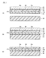
以下、本発明を、図面に示す実施形態に基づき説明する。
図1は本発明の一実施形態に係る積層セラミックコンデンサの概略断面図、
図2(A)〜図2(C)は本発明の一実施形態に係る電極層およびグリーンシートの形成方法を示す要部断面図、
図3(A)〜図3(C)は本発明の一実施形態に係る接着層の形成方法を示す要部断面図、
図4(A)〜図4(C)、図5(A)、図5(B)および図6(A)、図6(B)は本発明の一実施形態に係る電極層を有するグリーンシートの積層方法を示す要部断面図、
図7(A)〜図7(C)および図8(A)〜図8(C)は本発明の他の実施形態に係る電極層を有するグリーンシートの積層方法を示す要部断面図である。
Hereinafter, the present invention will be described based on embodiments shown in the drawings.
FIG. 1 is a schematic cross-sectional view of a multilayer ceramic capacitor according to an embodiment of the present invention.
2 (A) to 2 (C) are main part cross-sectional views showing a method for forming an electrode layer and a green sheet according to an embodiment of the present invention,
3 (A) to 3 (C) are main part cross-sectional views showing a method for forming an adhesive layer according to an embodiment of the present invention,
4 (A) to 4 (C), FIG. 5 (A), FIG. 5 (B), FIG. 6 (A), and FIG. 6 (B) are green sheets having electrode layers according to an embodiment of the present invention. Cross-sectional view of the main part showing the lamination method of
7 (A) to 7 (C) and FIGS. 8 (A) to 8 (C) are principal part cross-sectional views showing a method for laminating green sheets having electrode layers according to another embodiment of the present invention. .
まず、本発明に係る方法により製造される電子部品の一実施形態として、積層セラミックコンデンサの全体構成について説明する。
図1に示すように、本実施形態に係る積層セラミックコンデンサ2は、コンデンサ素体4と、第1端子電極6と第2端子電極8とを有する。コンデンサ素体4は、誘電体層10と、内部電極層12とを有し、誘電体層10の間に、これらの内部電極層12が交互に積層してある。交互に積層される一方の内部電極層12は、コンデンサ素体4の第1端部の外側に形成してある第1端子電極6の内側に対して電気的に接続してある。また、交互に積層される他方の内部電極層12は、コンデンサ素体4の第2端部の外側に形成してある第2端子電極8の内側に対して電気的に接続してある。
First, an overall configuration of a multilayer ceramic capacitor will be described as an embodiment of an electronic component manufactured by the method according to the present invention.
As shown in FIG. 1, the multilayer
本実施形態では、内部電極層12は、後で詳細に説明するように、図2に示すように、キャリアシート20上に剥離層22を介して、電極層12aを所定パターンで形成することにより、製造される。
In this embodiment, as will be described in detail later, the
誘電体層10の材質は、特に限定されず、たとえばチタン酸カルシウム、チタン酸ストロンチウムおよび/またはチタン酸バリウムなどの誘電体材料で構成される。各誘電体層10の厚みは、特に限定されないが、数μm〜数百μmのものが一般的である。特に本実施形態では、好ましくは3μm以下、より好ましくは1.5μm以下に薄層化されている。
The material of the
端子電極6および8の材質も特に限定されないが、通常、銅や銅合金、ニッケルやニッケル合金などが用いられるが、銀や銀とパラジウムの合金なども使用することができる。端子電極6および8の厚みも特に限定されないが、通常10〜50μm程度である。
Although the material of the
積層セラミックコンデンサ2の形状やサイズは、目的や用途に応じて適宜決定すればよい。積層セラミックコンデンサ2が直方体形状の場合は、通常、縦(0.6〜5.6mm、好ましくは0.6〜3.2mm)×横(0.3〜5.0mm、好ましくは0.3〜1.6mm)×厚み(0.1〜1.9mm、好ましくは0.3〜1.6mm)程度である。
The shape and size of the multilayer
次に、本実施形態に係る積層セラミックコンデンサ2の製造方法の一例を説明する。
本実施形態では、まず、図2(A)〜図2(C)に示す方法により、キャリアシート20上に、剥離層22、電極層12a、余白パターン層24およびグリーンシート10aをそれぞれ形成する。
Next, an example of a method for manufacturing the multilayer
In the present embodiment, first, the
まず、図2(A)に示すように、キャリアシート20上に剥離層22を形成する。
キャリアシート20としては、たとえばPETフィルムなどが用いられ、剥離性を改善するために、シリコン樹脂などがコーティングしてあるものが好ましい。キャリアシート20の厚みは、特に限定されないが、好ましくは、5〜100μmである。
First, as shown in FIG. 2A, a
As the
剥離層22は、バインダとして、少なくとも粘着力の低い樹脂を含有する。また、この剥離層22は、バインダ以外に、可塑剤と、離型剤と、剥離剤とを含んでも良い。
The
本実施形態では、剥離層22の厚みは、好ましくは0.02〜0.2μm、より好ましくは0.02〜0.1μm、さらに好ましくは0.05〜0.1μmとする。剥離層22の厚みが薄すぎると、剥離層22を形成した効果が得られなくなる傾向にある。また、剥離層22が厚すぎると、剥離時における剥離層22の電極層12a側への残存量が、多くなってしまい、脱バインダ時のクラックの発生率が悪化してしまう傾向にある。
In the present embodiment, the thickness of the
剥離層22の形成方法としては、特に限定されないが、きわめて薄く形成する必要があるために、たとえばワイヤーバーコーターまたはダイコーターを用いる塗布方法が好ましい。剥離層22は、塗布後に、好ましくは、乾燥温度50〜100°C、乾燥時間1〜10分の条件で乾燥される。
The method for forming the
剥離層22のバインダに含有される粘着力の低い樹脂としては、粘着強度が低く、キャリアフィルム20上に良好に形成可能な樹脂であれば特に限定されないが、たとえば、アクリル樹脂、ブチラール樹脂、アセタール樹脂、エポキシ樹脂、ポリオレフィン、ポリウレタン、ポリスチレン、尿素樹脂、ポリイミド、または、これらの共重合体などが挙げられる。なかでも、低粘着力や支持シートとの親和性の観点より、アクリル樹脂、ブチラール樹脂、アセタール樹脂およびエポキシ樹脂から選ばれる1種または2種以上を使用することが好ましい。これらの樹脂を用いることで、剥離層を薄くした場合においても、剥離層を形成した効果が十分に発揮される。また、本実施形態においては、粘着力の低い樹脂のガラス転移温度Tgは高いほうが好ましく、特に、Tgは室温以上であることが好ましい。Tgが室温以上である樹脂を使用することにより、剥離層20の剥離強度をより低くすることができる。なお、剥離層20中には、上述した粘着力の低い樹脂以外の各種バインダが含有されていても良い。
The resin having a low adhesive strength contained in the binder of the
上記アクリル樹脂としては、アクリル酸エステル(たとえば、アクリル酸メチル、アクリル酸エチルなど)およびメタクリル酸エステル(たとえば、メタクリル酸メチル、メタクリル酸エチル、メタクリル酸グリシジルなど)の単独重合体やこれらの共重合体などが使用できる。 Examples of the acrylic resin include homopolymers of acrylic acid esters (for example, methyl acrylate, ethyl acrylate, etc.) and methacrylic acid esters (for example, methyl methacrylate, ethyl methacrylate, glycidyl methacrylate), and their co-polymers. Coalescence etc. can be used.
上記ブチラール樹脂としては、たとえば、ポリビニルブチラールなどが挙げらる。ポリビニルブチラールの重合度およびブチラール化度は、特に限定されないが、通常、重合化度は1000〜3600程度、ブチラール化度は63〜77%程度とする。 Examples of the butyral resin include polyvinyl butyral. The degree of polymerization and the degree of butyralization of polyvinyl butyral are not particularly limited, but usually the degree of polymerization is about 1000 to 3600 and the degree of butyral is about 63 to 77%.
上記アセタール樹脂としては、たとえば、ポリビニルアセタールなどが挙げらる。ポリビニルアセタールの重合度およびアセタール化度は、特に限定されないが、通常、重合化度は1000〜3600程度、アセタール化度は62〜74%程度とする。アセタール樹脂は、比較的高いTgを有するため、好適に用いることができる。 Examples of the acetal resin include polyvinyl acetal. The degree of polymerization and the degree of acetalization of polyvinyl acetal are not particularly limited, but usually the degree of polymerization is about 1000 to 3600, and the degree of acetalization is about 62 to 74%. Since the acetal resin has a relatively high Tg, it can be suitably used.
剥離層22のための可塑剤としては、特に限定されないが、たとえばフタル酸エステル、アジピン酸、燐酸エステル、グリコール類などが例示される。剥離層22に含まれる可塑剤は、グリーンシート10aに含まれる可塑剤と同じでも異なっていても良い。
Although it does not specifically limit as a plasticizer for the
剥離層22のための剥離剤としては、特に限定されないが、たとえばパラフィン、ワックス、シリコーン油などが例示される。剥離層22に含まれる剥離剤は、グリーンシート10aに含まれる剥離剤と同じでも異なっていても良い。
The release agent for the
可塑剤の含有量は、剥離層22中に、粘着力の低い樹脂100質量部に対して、0〜200質量部、好ましくは20〜200質量部、さらに好ましくは50〜100質量部とする。ただし、剥離層22にブチラール樹脂を含有させる場合には、可塑剤を含ませない方がよい。
The content of the plasticizer is 0 to 200 parts by mass, preferably 20 to 200 parts by mass, and more preferably 50 to 100 parts by mass with respect to 100 parts by mass of the resin having low adhesive strength in the
剥離剤は、剥離層22中に、バインダ100質量部に対して、0〜100質量部、好ましくは2〜50質量部、さらに好ましくは5〜20質量部で含まれることが好ましい。
The release agent is preferably contained in the
剥離層22をキャリアシート20の表面に形成した後、図2(B)に示すように、剥離層22の表面に、焼成後に内部電極層12を構成することになる電極層12aを所定パターンで形成する。電極層12aの厚みは、1.5μm以下とすることが好ましい。電極層12aは、単一の層で構成してあってもよく、あるいは2以上の組成の異なる複数の層で構成してあってもよい。なお、本実施形態では、剥離層22上に電極層12aを形成するため、電極はじきを有効に防止することができ、電極層12aの形成を良好に、かつ、高精度に行うことができる。
After the
電極層12aは、たとえば電極ペーストを用いる印刷法などの厚膜形成方法、あるいは蒸着、スパッタリングなどの薄膜法により、剥離層22の表面に形成することができる。厚膜法の1種であるスクリーン印刷法あるいはグラビア印刷法により、剥離層22の表面に電極層12aを形成する場合には、以下のようにして行う。
The
まず、電極ペーストを準備する。電極ペーストは、各種導電性金属や合金からなる導電体材料、あるいは焼成後に上記した導電体材料となる各種酸化物、有機金属化合物、またはレジネート等と、有機ビヒクルとを混練して調製する。 First, an electrode paste is prepared. The electrode paste is prepared by kneading a conductive material made of various conductive metals or alloys, or various oxides, organometallic compounds, resinates, or the like, which become the conductive material described above after firing, and an organic vehicle.
電極ペーストを製造する際に用いる導体材料としては、NiやNi合金さらにはこれらの混合物を用いる。このような導体材料は、球状、リン片状等、その形状に特に制限はなく、また、これらの形状のものを混合したものであってもよい。導体材料の平均粒子径は、通常、0.1〜2μm、好ましくは0.2〜1μm程度のものを用いればよい。 As a conductive material used when manufacturing the electrode paste, Ni, Ni alloy, or a mixture thereof is used. There are no particular restrictions on the shape of such a conductor material, such as a spherical shape or a flake shape, and a mixture of these shapes may also be used. The average particle diameter of the conductor material is usually 0.1 to 2 μm, preferably about 0.2 to 1 μm.
有機ビヒクルは、バインダおよび溶剤を含有するものである。バインダとしては、例えばエチルセルロース、アクリル樹脂、ポリビニルブチラールなどのブチラール樹脂、ポリビニルアセタールなどのアセタール樹脂、ポリビニルアルコール、ポリオレフィン、ポリウレタン、ポリスチレン、または、これらの共重合体などが例示されるが、なかでも、エチルセルロースや、ポリビニルブチラールなどのブチラール樹脂が好ましい。 The organic vehicle contains a binder and a solvent. Examples of the binder include ethyl cellulose, acrylic resins, butyral resins such as polyvinyl butyral, acetal resins such as polyvinyl acetal, polyvinyl alcohol, polyolefin, polyurethane, polystyrene, and copolymers thereof, among others. Butyral resins such as ethyl cellulose and polyvinyl butyral are preferred.
バインダは、電極ペースト中に、導体材料(金属粉末)100質量部に対して、好ましくは4〜10質量部含まれる。溶剤としては、例えばテルピネオール、ブチルカルビトール、ケロシン、アセトン、イソボニルアセテート等公知のものはいずれも使用可能である。溶剤含有量は、ペースト全体に対して、好ましくは20〜55質量%程度とする。 The binder is preferably contained in the electrode paste in an amount of 4 to 10 parts by mass with respect to 100 parts by mass of the conductive material (metal powder). Any known solvent such as terpineol, butyl carbitol, kerosene, acetone, isobornyl acetate can be used as the solvent. The solvent content is preferably about 20 to 55% by mass with respect to the entire paste.
グリーンシートとの接着性を改善するために、電極ペーストには、可塑剤または粘着剤が含まれることが好ましい。可塑剤としては、フタル酸ジオクチルやフタル酸ベンジルブチルなどのフタル酸エステル、アジピン酸、燐酸エステル、グリコール類などが例示される。可塑剤の添加量は、電極ペースト中に、バインダ100質量部に対して、好ましくは10〜300質量部、さらに好ましくは10〜200質量部である。なお、可塑剤または粘着剤の添加量が多すぎると、焼成前の電極層の強度が著しく低下する傾向にある。また、電極ペースト中には、可塑剤や粘着剤を添加して、電極ペーストの接着性や粘着性を向上させることが好ましい。 In order to improve the adhesion to the green sheet, the electrode paste preferably contains a plasticizer or a pressure-sensitive adhesive. Examples of the plasticizer include phthalate esters such as dioctyl phthalate and benzylbutyl phthalate, adipic acid, phosphate esters, glycols, and the like. The addition amount of the plasticizer is preferably 10 to 300 parts by mass, more preferably 10 to 200 parts by mass with respect to 100 parts by mass of the binder in the electrode paste. In addition, when there is too much addition amount of a plasticizer or an adhesive, there exists a tendency for the intensity | strength of the electrode layer before baking to fall remarkably. Moreover, it is preferable to add the plasticizer and the adhesive to the electrode paste to improve the adhesiveness and adhesiveness of the electrode paste.
剥離層22の表面に、所定パターンの電極ペースト層を印刷法で形成した後、またはその前に、電極層12aが形成されていない剥離層22の表面に、電極層12aと実質的に同じ厚みの余白パターン層24を形成する。余白パターン層24は、後に詳述するグリーンシート10aと同様な材質で構成される。また、余白パターン層24は、電極層12aあるいは、後に詳述するグリーンシート10aと同様な方法で形成することができる。電極層12aおよび余白パターン層24は、必要に応じて乾燥される。乾燥温度は、特に限定されないが、好ましくは70〜120°Cであり、乾燥時間は、好ましくは5〜15分である。
After or before the electrode paste layer having a predetermined pattern is formed on the surface of the
次いで、図2(C)に示すように、剥離層22上に形成した電極層12aおよび余白パターン層24の表面に、グリーンシート10aを形成する。グリーンシート10aは、焼成後に図1に示す誘電体層10を構成することとなる。なお、本実施形態では、接着層を用いることなく、電極層12aおよび余白パターン層24の表面に、グリーンシート10aを形成することができる。グリーンシート10aを、接着層を用いることなく、電極層12aおよび余白パターン層24上に形成することにより、積層時の接着力を高く保ちつつ、かつ、製造工程の簡略化および製造コストの低減を図ることができる。
Next, as illustrated in FIG. 2C, the
グリーンシート10aは、誘電体原料を含有する誘電体ペーストを用いて、ダイコーティング法などにより、電極層12aおよび余白パターン層24の表面に形成される。グリーンシート10aは、好ましくは0.5〜30μm、より好ましくは0.5〜10μm程度の厚みで形成され、電極層12aおよび余白パターン層24上に形成された後に乾燥される。グリーンシート10aの乾燥温度は、好ましくは50〜100°Cであり、乾燥時間は、好ましくは1〜20分である。乾燥後のグリーンシート10aの厚みは、乾燥前に比較して、5〜25%の厚みに収縮する。乾燥後のグリーンシートの厚みは、1.5μm以下が好ましく、さらに、グリーンシート10aは、グリーンシート10aと電極層12aとの合計の厚みが3.0μm以下となるように形成することが好ましい。
The
グリーンシート10aを製造するための誘電体ペーストは、通常、誘電体原料と有機ビヒクルとを混練して得られた有機溶剤系ペースト、または水系ペーストで構成される。
The dielectric paste for producing the
誘電体原料としては、複合酸化物や酸化物となる各種化合物、たとえば炭酸塩、硝酸塩、水酸化物、有機金属化合物などから適宜選択され、混合して用いることができる。誘電体原料は、通常、平均粒子径が0.3μm以下、好ましくは0.2μm以下の粉末として用いられる。なお、極めて薄いグリーンシートを形成するためには、グリーンシート厚みよりも細かい粉末を使用することが望ましい。 As the dielectric material, various compounds to be complex oxides and oxides, for example, carbonates, nitrates, hydroxides, organometallic compounds, and the like are appropriately selected and used by mixing. The dielectric material is usually used as a powder having an average particle size of 0.3 μm or less, preferably 0.2 μm or less. In order to form an extremely thin green sheet, it is desirable to use a powder finer than the thickness of the green sheet.
有機ビヒクルとは、バインダを有機溶剤中に溶解したものである。有機ビヒクルに用いられるバインダとしては、特に限定されず、エチルセルロース、ポリビニルブチラール、アクリル樹脂などの通常の各種バインダが用いられるが、好ましくは、アクリル樹脂、あるいはポリビニルブチラールなどのブチラール樹脂が用いられる。 An organic vehicle is obtained by dissolving a binder in an organic solvent. The binder used in the organic vehicle is not particularly limited, and various ordinary binders such as ethyl cellulose, polyvinyl butyral, and acrylic resin are used. Preferably, butyral resin such as acrylic resin or polyvinyl butyral is used.
また、有機ビヒクルに用いられる有機溶剤も特に限定されず、テルピネオール、アルコール、ブチルカルビトール、アセトン、メチルエチルケトン(MEK)、トルエン、キシレン、酢酸エチル、ステアリン酸ブチル、イソボニルアセテートなどの有機溶剤が用いられる。また、水系ペーストにおけるビヒクルは、水に水溶性バインダを溶解させたものである。水溶性バインダとしては特に限定されず、ポリビニルアルコール、メチルセルロース、ヒドロキシエチルセルロース、水溶性アクリル樹脂、エマルジョンなどが用いられる。誘電体ペースト中の各成分の含有量は特に限定されず、通常の含有量、たとえばバインダは1〜5質量%程度、溶剤(または水)は10〜50質量%程度とすればよい。 The organic solvent used in the organic vehicle is not particularly limited, and organic solvents such as terpineol, alcohol, butyl carbitol, acetone, methyl ethyl ketone (MEK), toluene, xylene, ethyl acetate, butyl stearate, isobornyl acetate are used. It is done. Further, the vehicle in the aqueous paste is obtained by dissolving a water-soluble binder in water. The water-soluble binder is not particularly limited, and polyvinyl alcohol, methyl cellulose, hydroxyethyl cellulose, water-soluble acrylic resin, emulsion and the like are used. The content of each component in the dielectric paste is not particularly limited, and the normal content, for example, the binder may be about 1 to 5% by mass, and the solvent (or water) may be about 10 to 50% by mass.
誘電体ペースト中には、必要に応じて各種分散剤、可塑剤、誘電体、ガラスフリット、絶縁体、帯電助剤などから選択される添加物が含有されても良い。ただし、これらの総含有量は、10質量%以下とすることが望ましい。可塑剤としては、フタル酸ジオクチルやフタル酸ベンジルブチルなどのフタル酸エステル、アジピン酸、燐酸エステル、グリコール類などが例示される。バインダ樹脂として、ブチラール樹脂を用いる場合には、可塑剤は、バインダ樹脂100質量部に対して、25〜100質量部の含有量であることが好ましい。可塑剤が少なすぎると、グリーンシートが脆くなる傾向にあり、多すぎると、可塑剤が滲み出し、取り扱いが困難である。 The dielectric paste may contain additives selected from various dispersants, plasticizers, dielectrics, glass frit, insulators, charging aids, and the like as necessary. However, the total content of these is preferably 10% by mass or less. Examples of the plasticizer include phthalate esters such as dioctyl phthalate and benzylbutyl phthalate, adipic acid, phosphate esters, glycols, and the like. When using a butyral resin as the binder resin, the plasticizer preferably has a content of 25 to 100 parts by mass with respect to 100 parts by mass of the binder resin. If the amount of the plasticizer is too small, the green sheet tends to be brittle. If the amount is too large, the plasticizer oozes out and is difficult to handle.
次いで、上記のキャリアシート20とは別に、図3(A)に示すように、第2支持シートとしてのキャリアシート26の表面に接着層28が形成してある接着層転写用シートを準備する。キャリアシート26は、キャリアシート20と同様なシートで構成される。キャリアシート26の厚みは、キャリアシート20と同じ厚みとしても良いし、また異なる厚みとしても良い。
Next, separately from the
接着層28は、バインダと、可塑剤とを含む。接着層28には、グリーンシート10aを構成する誘電体と同じ誘電体粒子を含ませても良いが、誘電体粒子の粒径よりも厚みが薄い接着層を形成する場合には、誘電体粒子を含ませない方がよい。また、接着層28に誘電体粒子を含ませる場合には、その誘電体粒子の粒径は、グリーンシートに含まれる誘電体粒子の粒径より小さいことが好ましい。
The
接着層28のためのバインダとしては、たとえば、アクリル樹脂、ポリビニルブチラールなどのブチラール樹脂、ポリビニルアセタールなどのアセタール樹脂、ポリビニルアルコール、ポリオレフィン、ポリウレタン、ポリスチレン、または、これらの共重合体からなる有機質、またはエマルジョンで構成される。本実施形態では、上記バインダとして、アクリル樹脂、あるいはポリビニルブチラール等のブチラール樹脂を用いることが、特に好ましい。また、接着層28に含まれるバインダは、グリーンシート10aに含まれるバインダと同じでも異なっていても良いが同じであることが好ましい。
As the binder for the
接着層28のための可塑剤としては、特に限定されないが、たとえばフタル酸ジオクチルやフタル酸ビス(2−エチルヘキシル)などのフタル酸エステル、アジピン酸、燐酸エステル、グリコール類などが例示される。接着層28に含まれる可塑剤は、グリーンシート10aに含まれる可塑剤と同じでも異なっていても良い。
Although it does not specifically limit as a plasticizer for the
可塑剤は、接着層28中に、バインダ100質量部に対して、0〜200質量部、好ましくは20〜200質量部、さらに好ましくは30〜70質量部で含まれることが好ましい。
The plasticizer is preferably contained in the
接着層28は、さらに帯電除剤を含むことが好ましく、当該帯電除剤は、イミダゾリン系界面活性剤の中の1つを含み、帯電除剤の重量基準添加量は、バインダ(有機高分子材料)の重量基準添加量以下であることが好ましい。帯電除剤の含有量は、接着層28中に、バインダ100質量部に対して、0〜200質量部、好ましくは20〜200質量部、さらに好ましくは50〜100質量部で含まれることが好ましい。
The
接着層28の厚みは、好ましくは0.02〜0.3μm、より好ましくは0.05〜0.1μmであり、しかもグリーンシートに含まれる誘電体粒子の平均粒径よりも薄いことが好ましい。また、接着層28の厚みが、グリーンシート10aの厚みの1/10以下であることが好ましい。
The thickness of the
接着層28の厚みが薄すぎると、接着力が低下し、厚すぎると、その接着層の厚みに依存して焼結後の素子本体の内部に隙間ができやすく、その体積分の静電容量が著しく低下する傾向にある。
If the thickness of the
接着層28は、第2支持シートとしてのキャリアシート26の表面に、たとえばバーコータ法、ダイコータ法、リバースコータ法、ディップコーター法、キスコーター法などの方法により形成され、必要に応じて乾燥される。乾燥温度は、特に限定されないが、好ましくは室温〜80°Cであり、乾燥時間は、好ましくは1〜5分である。
The
次いで、図2(C)に示す電極層12aおよび余白パターン層24上に形成されたグリーンシート10aの表面に、接着層28を形成し、図3(C)に示す積層体ユニットU1aを得る。本実施形態においては、接着層28の形成方法として、転写法を採用している。すなわち、図3(A)、図3(B)に示すように、キャリアシート26の接着層28を、グリーンシート10aの表面に押し付け、加熱加圧して、その後キャリアシート26を剥がすことにより、図3(C)に示すように、接着層28を、グリーンシート10aの表面に転写し、積層体ユニットU1aを得る。
Next, an
接着層28を、転写法により形成することにより、接着層の成分のグリーンシート10a、あるいは電極層12aや余白パターン層24への染み込みを有効に防止することができる。そのため、グリーンシート10a、あるいは電極層12aや余白パターン層24の組成に悪影響を与えるおそれがない。さらに、接着層28を薄く形成した場合でも、接着層の成分が、グリーンシート10a、あるいは電極層12aや余白パターン層24へ染み込むことがないため、接着性を高く保つことができる。
By forming the
転写時の加熱温度は、40〜100°Cが好ましく、また、加圧力は、0.2〜15MPaが好ましい。加圧は、プレスによる加圧でも、カレンダロールによる加圧でも良いが、一対のロールにより行うことが好ましい。 The heating temperature during transfer is preferably 40 to 100 ° C., and the applied pressure is preferably 0.2 to 15 MPa. The pressurization may be a pressurization or a calender roll, but is preferably performed by a pair of rolls.
次いで、電極層12aおよび余白パターン層24、グリーンシート10a、接着層28の順に積層された積層体ユニットを、複数積層することにより、グリーンチップを形成する。積層体ユニットの積層は、図4〜図6に示すように、接着層28を介して、各積層体ユニット同士を接着することにより行う。以下、積層方法について説明する。
Next, a green chip is formed by laminating a plurality of laminate units in which the
まず、図4(A)、図4(B)に示すように、上記にて作製した積層体ユニットU1aから第1支持シート20を剥がす。次に、図4(C)に示すように、積層体ユニットU1aを、外層用のグリーンシート30(電極層が形成されていない10〜30μmの厚みのグリーンシートを、複層積層した厚み100〜200μmの積層体)上に積層する。
First, as shown to FIG. 4 (A) and FIG. 4 (B), the
本実施形態においては、積層体ユニットU1aは、剥離層22を介してキャリアシート20上に形成されているため、キャリアシート20の剥離を、良好に行うことができる。また、剥離時に、積層体ユニットU1aの電極層12aや余白パターン層24を破損させることもない。なお、剥離層22は、キャリアシート20とともに、積層体ユニットU1aから剥離されることが好ましいが、少量程度なら、積層体ユニットU1a側に残存しても構わない。この場合においても、その残存している剥離層22は、積層体ユニットU1aを構成するグリーンシート10aや電極層12aに比較して十分薄いため、問題となることはない。
In this embodiment, since the laminated body unit U1a is formed on the
次に、図5(A)に示すように、積層体ユニットU1aと同様の方法により作製した別の積層体ユニットU1bを準備する。準備した積層体ユニットU1bから、第1支持シート20を剥がし、図5(B)に示すように、キャリアシート20が剥離された積層体ユニットU1bと、積層体ユニットU1aとを、積層体ユニットU1aの接着層28を介して、接着し、積層する。
Next, as shown to FIG. 5 (A), another laminated body unit U1b produced by the method similar to the laminated body unit U1a is prepared. The
次に、図6(A)、図6(B)に示すように、同様にして、積層体ユニットU1b上に、別の積層体ユニットU1cを、積層体ユニットU1bの接着層28を介して、接着し、積層する。そして、この図6(A)、図6(B)に示す工程を繰り返すことにより、複数の積層体ユニットを積層する。次いで、この積層体の上面に、外層用のグリーンシート30を積層し、最終加圧を行い、その後、積層体を所定サイズに切断し、グリーンチップを形成する。なお、最終加圧時の圧力は、好ましくは10〜200MPaとし、また、加熱温度は、好ましくは、40〜100°Cとする。
Next, as shown in FIG. 6 (A) and FIG. 6 (B), in the same manner, another laminate unit U1c is placed on the laminate unit U1b via the
このグリーンチップは、脱バインダ処理、焼成処理が行われ、そして、誘電体層を再酸化させるため、熱処理が行われる。 This green chip is subjected to binder removal processing and firing processing, and heat treatment is performed to reoxidize the dielectric layer.
脱バインダ処理は、通常の条件で行えばよいが、内部電極層の導電体材料としてNiやNi合金等の卑金属を用いる場合、下記の条件で行うことが好ましい。 The binder removal treatment may be performed under normal conditions, but when a base metal such as Ni or Ni alloy is used as the conductor material of the internal electrode layer, it is preferably performed under the following conditions.
昇温速度:5〜300℃/時間、特に10〜50℃/時間、
保持温度:200〜400℃、特に250〜350℃、
保持時間:0.5〜20時間、特に1〜10時間、
雰囲気 :加湿したN2 とH2 との混合ガス。
Temperature increase rate: 5 to 300 ° C./hour, particularly 10 to 50 ° C./hour,
Holding temperature: 200-400 ° C, especially 250-350 ° C,
Retention time: 0.5 to 20 hours, especially 1 to 10 hours,
Atmosphere: A mixed gas of humidified N 2 and H 2 .
焼成条件は、下記の条件が好ましい。
昇温速度:50〜500℃/時間、特に200〜300℃/時間、
保持温度:1100〜1300℃、特に1150〜1250℃、
保持時間:0.5〜8時間、特に1〜3時間、
冷却速度:50〜500℃/時間、特に200〜300℃/時間、
雰囲気ガス:加湿したN2 とH2 との混合ガス等。
The firing conditions are preferably the following conditions.
Temperature increase rate: 50 to 500 ° C./hour, particularly 200 to 300 ° C./hour,
Holding temperature: 1100-1300 ° C., in particular 1150-1250 ° C.
Retention time: 0.5-8 hours, especially 1-3 hours,
Cooling rate: 50 to 500 ° C./hour, particularly 200 to 300 ° C./hour,
Atmospheric gas: A mixed gas of humidified N 2 and H 2 or the like.
ただし、焼成時の空気雰囲気中の酸素分圧は、10−2Pa以下、特に10−2〜10−8 Paにて行うことが好ましい。前記範囲を超えると、内部電極層が酸化する傾向にあり、また、酸素分圧があまり低すぎると、内部電極層の電極材料が異常焼結を起こし、途切れてしまう傾向にある。 However, the oxygen partial pressure in the air atmosphere during firing is preferably 10 −2 Pa or less, particularly 10 −2 to 10 −8 Pa. If the above range is exceeded, the internal electrode layer tends to oxidize, and if the oxygen partial pressure is too low, the electrode material of the internal electrode layer tends to abnormally sinter and tend to break.
このような焼成を行った後の熱処理は、保持温度または最高温度を、好ましくは1000℃以上、さらに好ましくは1000〜1100℃として行うことが好ましい。熱処理時の保持温度または最高温度が、前記範囲未満では誘電体材料の酸化が不十分なために絶縁抵抗寿命が短くなる傾向にあり、前記範囲をこえると内部電極のNiが酸化し、容量が低下するだけでなく、誘電体素地と反応してしまい、寿命も短くなる傾向にある。熱処理の際の酸素分圧は、焼成時の還元雰囲気よりも高い酸素分圧であり、好ましくは10−3Pa〜1Pa、より好ましくは10−2Pa〜1Paである。前記範囲未満では、誘電体層2の再酸化が困難であり、前記範囲をこえると内部電極層12が酸化する傾向にある。
The heat treatment after such firing is preferably carried out at a holding temperature or maximum temperature of preferably 1000 ° C. or higher, more preferably 1000 to 1100 ° C. If the holding temperature or maximum temperature during heat treatment is less than the above range, the dielectric material is insufficiently oxidized and the insulation resistance life tends to be shortened. In addition to a decrease, it tends to react with the dielectric substrate and shorten its lifetime. The oxygen partial pressure during the heat treatment is higher than the reducing atmosphere during firing, and is preferably 10 −3 Pa to 1 Pa, more preferably 10 −2 Pa to 1 Pa. If it is less than the above range, it is difficult to reoxidize the
そして、そのほかの熱処理条件は下記の条件が好ましい。
保持時間:0〜6時間、特に2〜5時間、
冷却速度:50〜500℃/時間、特に100〜300℃/時間、
雰囲気用ガス:加湿したN2 ガス等。
The other heat treatment conditions are preferably the following conditions.
Retention time: 0-6 hours, especially 2-5 hours,
Cooling rate: 50 to 500 ° C./hour, in particular 100 to 300 ° C./hour,
Atmospheric gas: humidified N 2 gas or the like.
なお、N2 ガスや混合ガス等を加湿するには、例えば加温した水にガスを通し、バブリングする装置等を使用すればよい。この場合、水温は0〜75℃程度が好ましい。また脱バインダ処理、焼成および熱処理は、それぞれを連続して行っても、独立に行ってもよい。これらを連続して行なう場合、脱バインダ処理後、冷却せずに雰囲気を変更し、続いて焼成の際の保持温度まで昇温して焼成を行ない、次いで冷却し、熱処理の保持温度に達したときに雰囲気を変更して熱処理を行なうことが好ましい。一方、これらを独立して行なう場合、焼成に際しては、脱バインダ処理時の保持温度までN2 ガスあるいは加湿したN2 ガス雰囲気下で昇温した後、雰囲気を変更してさらに昇温を続けることが好ましく、熱処理時の保持温度まで冷却した後は、再びN2 ガスあるいは加湿したN2 ガス雰囲気に変更して冷却を続けることが好ましい。また、熱処理に際しては、N2 ガス雰囲気下で保持温度まで昇温した後、雰囲気を変更してもよく、熱処理の全過程を加湿したN2 ガス雰囲気としてもよい。 Note that to wet the N 2 gas and mixed gas, etc., through a gas, for example, water heated, may be used to bubbling to device. In this case, the water temperature is preferably about 0 to 75 ° C. The binder removal treatment, firing and heat treatment may be performed continuously or independently. When performing these continuously, after removing the binder, the atmosphere is changed without cooling, and then the temperature is raised to the holding temperature at the time of baking to perform baking, and then cooled to reach the heat treatment holding temperature. Sometimes it is preferable to perform heat treatment by changing the atmosphere. On the other hand, when performing these independently, at the time of firing, after raising the temperature under N 2 gas atmosphere with N 2 gas or wet to the holding temperature of the binder removal processing, further continuing the heating to change the atmosphere Preferably, after cooling to the holding temperature at the time of heat treatment, it is preferable to change to N 2 gas or a humidified N 2 gas atmosphere and continue cooling. In the heat treatment, the temperature may be changed to a holding temperature in an N 2 gas atmosphere, and the atmosphere may be changed, or the entire process of the heat treatment may be a humidified N 2 gas atmosphere.
このようにして得られた焼結体(素子本体4)には、例えばバレル研磨、サンドプラスト等にて端面研磨を施し、端子電極用ペーストを焼きつけて端子電極6,8が形成される。端子電極用ペーストの焼成条件は、例えば、加湿したN2 とH2 との混合ガス中で600〜800℃にて10分間〜1時間程度とすることが好ましい。そして、必要に応じ、端子電極6,8上にめっき等を行うことによりパッド層を形成する。なお、端子電極用ペーストは、上記した電極ペーストと同様にして調製すればよい。
このようにして製造された本発明の積層セラミックコンデンサは、ハンダ付等によりプリント基板上などに実装され、各種電子機器等に使用される。
The sintered body (element body 4) thus obtained is subjected to end surface polishing by, for example, barrel polishing, sand plast, etc., and
The multilayer ceramic capacitor of the present invention thus manufactured is mounted on a printed circuit board by soldering or the like and used for various electronic devices.
本実施形態では、非接着欠陥(ノンラミネーション)が比較的問題とならない工程では、接着層を用いることなく積層を行う。しかも、非接着欠陥(ノンラミネーション)が起こりやすい工程では、接着層を介して積層を行う。すなわち、電極層12a上へグリーンシート10aを形成する際には、接着層を用いないため、製造工程の簡略化や製造コストの低減を図ることができる。さらに、電極層12aを有するグリーンシート10aを積層する際には、接着層28を介して積層を行うため、接着性の向上、および非接着欠陥(ノンラミネーション)の低減を図ることができる。そのため、本実施形態の製造方法によると、グリーンシートを極めて薄くした場合においても、接着性を高く保ちつつ、非接着欠陥(ノンラミネーション)を低減することができ、かつ、製造工程の簡略化や製造コストの低減が可能となる。
In this embodiment, lamination is performed without using an adhesive layer in a process where non-adhesion defects (non-lamination) are not a problem. Moreover, in a process where non-adhesion defects (non-lamination) are likely to occur, lamination is performed via an adhesive layer. That is, since the adhesive layer is not used when forming the
さらに本実施形態では、まず、キャリアシート20上に、粘着力の低い樹脂を含有する剥離層28を形成し、その上に、電極層12a、余白パターン層24およびグリーンシート10aを形成する。そのため、電極層形成時における電極はじきを有効に防止することができ、電極層を良好に、かつ、高精度に形成することができる。また、剥離層28を形成することにより、電極層12aとキャリアシート20との間の剥離強度を低くすることができ、電極層12aからの第1支持シートの剥離を、良好に行うことができ、また、剥離時に電極層12aを破損させることもない。
Furthermore, in this embodiment, first, the
なお、本発明は、上述した実施形態に限定されるものではなく、本発明の範囲内で種々に改変することができる。
たとえば、本発明の方法は、積層セラミックコンデンサの製造方法に限らず、その他の積層型電子部品の製造方法としても適用することが可能である。
The present invention is not limited to the above-described embodiment, and can be variously modified within the scope of the present invention.
For example, the method of the present invention can be applied not only to a method for manufacturing a multilayer ceramic capacitor but also to a method for manufacturing other multilayer electronic components.
また、上述した実施形態では、接着層28を転写法により形成したが、たとえば、ダイコーティング法などにより、グリーンシート10a上に、直接、塗布することにより接着層28を形成しても良い。
In the above-described embodiment, the
また、上述した実施形態では、各積層体ユニットを積層する前に、積層体ユニットからキャリアシート20を剥離して、積層体ユニットを積層したが、たとえば、図7、図8に示すように、積層体ユニットを積層した後に、キャリアシート20を剥離する工程を採用することもできる。
Further, in the above-described embodiment, before laminating each laminate unit, the
すなわち、図7(A)、図7(B)に示すように、まず、外層用のグリーンシート30上に、キャリアシート20を剥離していない積層体ユニットU1aを、接着層28を介して、接着し、積層する。次に、図7(C)に示すように、積層体ユニットU1aからキャリアシート20を剥離する。
That is, as shown in FIGS. 7A and 7B, first, the laminate unit U1a from which the
次いで、図8(A)〜図8(C)に示すように、同様にして、積層体ユニットU1a上に、別の積層体ユニットU1bを、積層体ユニットU1bの接着層28を介して、接着し、積層する。次いで、この図8(A)〜図8(C)に示す工程を繰り返すことにより、複数の積層体ユニットを積層する。そして、この積層体の上面に、外層用のグリーンシートを積層し、最終加圧を行い、その後、積層体を所定サイズに切断し、グリーンチップを形成することができる。
Next, as shown in FIGS. 8A to 8C, in the same manner, another laminate unit U1b is bonded onto the laminate unit U1a via the
なお、図7、図8に示す工程を採用した場合においては、接着層28の接着力を剥離層22の粘着力よりも強くすることにより、キャリアシート20を、選択的かつ容易に剥離することができるため、特に有効である。
In the case where the steps shown in FIGS. 7 and 8 are employed, the
以下、本発明を、さらに詳細な実施例に基づき説明するが、本発明は、これら実施例に限定されない。 Hereinafter, although this invention is demonstrated based on a more detailed Example, this invention is not limited to these Examples.
実施例1
まず、下記の各ペーストを準備した。
グリーンシート用ペースト
まず、添加物(副成分)原料として、(Ba,Ca)SiO3:1.48重量部、Y2O3:1.01重量部、MgCO3:0.72重量部、MnO:0.13重量部およびV2O5:0.045重量部を準備した。次に、準備したこれらの添加物(副成分)原料を混合し、添加物(副成分)原料混合物を得た。
Example 1
First, the following pastes were prepared.
Green Sheet Paste First, as additive (subcomponent) raw materials, (Ba, Ca) SiO 3 : 1.48 parts by weight, Y 2 O 3 : 1.01 parts by weight, MgCO 3 : 0.72 parts by weight, MnO : 0.13 parts by weight and V 2 O 5 : 0.045 parts by weight were prepared. Next, these additive (subcomponent) raw materials prepared were mixed to obtain an additive (subcomponent) raw material mixture.
次いで、上記にて得られた添加物原料混合物:4.3重量部、エタノール:3.11重量部、プロパノール:3.11重量部、キシレン:1.11重量部および分散剤:0.04重量部を、ボールミルを使用して混合粉砕し、添加物スラリーを得た。混合粉砕は、250ccポリエチレン製樹脂容器を用い、2mmφのZrO2メディア450gを投入し、周速45m/分および16時間の条件で行った。なお、粉砕後の添加物原料の粒径はメジアン径は0.1μmであった。 Subsequently, the additive raw material mixture obtained above: 4.3 parts by weight, ethanol: 3.11 parts by weight, propanol: 3.11 parts by weight, xylene: 1.11 parts by weight and dispersant: 0.04 parts by weight The parts were mixed and ground using a ball mill to obtain an additive slurry. The mixing and pulverization were carried out using a 250 cc polyethylene resin container, charged with 450 g of 2 mmφ ZrO 2 media under conditions of a peripheral speed of 45 m / min and 16 hours. The particle diameter of the additive raw material after pulverization was 0.1 μm in median diameter.
次いで、上記にて得られた添加物スラリー:11.65重量部、BaTiO3 粉末(BT−02/堺化学工業(株)):100重量部、エタノール:35.32重量部、プロパノール:35.32重量部、キシレン:16.32重量部、フタル酸ジオクチル(可塑剤):2.61重量部、ミネラルスピリット:7.3重量部、分散剤:2.36重量部、帯電助剤:0.42重量部、有機ビヒクル:33.74重量部、MEK:43.81重量部および2−ブトキシエタノール:43.81重量部を、ボールミルを使用して混合し、グリーンシート用ペーストを得た。なお、ボールミルによる混合は、500ccポリエチレン製樹脂容器を用い、2mmφのZrO2メディア900gを投入し、周速45m/分および20時間の条件で行った。また、上記の有機ビヒクルは、重合度1450、ブチラール化度69%のポリビニルブチラール樹脂(積水化学工業(株)製):15重量部を、エタノール:42.5重量部およびプロパノール:42.5重量部に、50°Cの温度で、撹拌溶解することにより作製した。すなわち、有機ビヒクル中の樹脂含有量(ポリビニルブチラール樹脂の量)は、15重量%とした。 Subsequently, the additive slurry obtained above: 11.65 parts by weight, BaTiO 3 powder (BT-02 / Sakai Chemical Industry Co., Ltd.): 100 parts by weight, ethanol: 35.32 parts by weight, propanol: 35. 32 parts by weight, xylene: 16.32 parts by weight, dioctyl phthalate (plasticizer): 2.61 parts by weight, mineral spirit: 7.3 parts by weight, dispersant: 2.36 parts by weight, charging aid: 0.8. 42 parts by weight, organic vehicle: 33.74 parts by weight, MEK: 43.81 parts by weight and 2-butoxyethanol: 43.81 parts by weight were mixed using a ball mill to obtain a paste for a green sheet. The mixing by the ball mill was carried out using a 500 cc polyethylene resin container, charging 900 g of 2 mmφ ZrO 2 media, and at a peripheral speed of 45 m / min and 20 hours. In addition, the above organic vehicle has 15 parts by weight of polyvinyl butyral resin having a polymerization degree of 1450 and a butyralization degree of 69% (manufactured by Sekisui Chemical Co., Ltd.): 42.5 parts by weight of ethanol and 42.5 parts by weight of propanol. This was prepared by stirring and dissolving in a part at a temperature of 50 ° C. That is, the resin content (amount of polyvinyl butyral resin) in the organic vehicle was 15% by weight.
内部電極用ペースト
まず、上記のグリーンシート用ペーストと同様にして、添加物原料混合物を作製した。
次いで、上記にて得られた添加物原料混合物:100重量部、アセトン:150重量部、ターピネオール:104.3重量部、ポリエチレングリコール系分散剤:1.5重量部を混合して、スラリー化し、得られたスラリーを粉砕機(アシザワ・ファインテック(株) 型式LMZ0.6)により粉砕し、添加物スラリーを得た。
Internal Electrode Paste First, an additive material mixture was prepared in the same manner as the above green sheet paste.
Next, the additive raw material mixture obtained above: 100 parts by weight, acetone: 150 parts by weight, terpineol: 104.3 parts by weight, polyethylene glycol dispersant: 1.5 parts by weight are mixed to make a slurry, The obtained slurry was pulverized by a pulverizer (Ashizawa Finetech Co., Ltd., model LMZ0.6) to obtain an additive slurry.
なお、スラリー中の添加物の粉砕は、ローターを周速14m/分の条件で回転させ、スラリーをベッセルとスラリータンクとの間を循環させることにより行った。なお、ベッセルには、直径0.1mmのZrO2ビーズを、ベッセル容量に対して、80%になるように充填し、また、粉砕は、全スラリーのベッセル内での滞留時間が5分となるように行った。なお、粉砕後の添加物のメジアン径は0.1μmであった。 Note that the additives in the slurry were pulverized by rotating the rotor at a peripheral speed of 14 m / min and circulating the slurry between the vessel and the slurry tank. The vessel is filled with ZrO 2 beads having a diameter of 0.1 mm so as to be 80% of the vessel volume, and the pulverization requires 5 minutes of residence time of the entire slurry in the vessel. Went so. The median diameter of the crushed additive was 0.1 μm.
次いで、粉砕後の添加物スラリーについて、エバポレータを用い、スラリー中からアセトンを蒸発させることにより除去し、添加物原料がターピネオールに分散された添加物スラリーを調製した。なお、アセトンを除去した後の添加物スラリー中の添加物原料濃度は49.3重量%であった。 Next, the crushed additive slurry was removed by evaporating acetone from the slurry using an evaporator to prepare an additive slurry in which the additive raw material was dispersed in terpineol. The additive raw material concentration in the additive slurry after removing acetone was 49.3% by weight.
次いで、ニッケル粉末(粒径0.2μm/川鉄工業(株)):100重量部、添加物スラリー:1.77重量部、BaTiO3 粉末(粒径0.05μm/堺化学工業(株)):19.14重量部、有機ビヒクル:56.25重量部、ポリエチレングリコール系分散剤:1.19重量部、フタル酸ジオクチル(可塑剤):2.25重量部、イソボニルアセテート:32.19重量部およびアセトン56重量部を、ボールミルを使用して混合してペースト化した。次いで、得られたペーストを、エバポレータおよび加熱機構を備えた攪拌装置を使用して、アセトンを蒸発させることにより、除去し、内部電極用ペーストを得た。 Next, nickel powder (particle size 0.2 μm / Kawatetsu Kogyo Co., Ltd.): 100 parts by weight, additive slurry: 1.77 parts by weight, BaTiO 3 powder (particle size 0.05 μm / Sakai Chemical Industry Co., Ltd.): 19.14 parts by weight, organic vehicle: 56.25 parts by weight, polyethylene glycol dispersant: 1.19 parts by weight, dioctyl phthalate (plasticizer): 2.25 parts by weight, isobornyl acetate: 32.19 parts by weight And 56 parts by weight of acetone were mixed using a ball mill to form a paste. Next, the obtained paste was removed by evaporating acetone by using an agitator equipped with an evaporator and a heating mechanism to obtain an internal electrode paste.
なお、ボールミルによる混合は、ボールミル中に2mmφのZrO2メディアを30容積%、上記各原料の混合物を60容積%充填し、周速45m/分および16時間の条件で行った。また、上記の有機ビヒクルは、70°Cの温度で、分子量13万のエチルセルロース樹脂:4重量部と分子量23万のエチルセルロース樹脂:4重量部とをイソボニルアセテート:92重量部に撹拌溶解することにより作製した。すなわち、有機ビヒクル中の樹脂含有量(エチルセルロース樹脂の量)は、8重量%とした。 The mixing with the ball mill was carried out under the conditions of a peripheral speed of 45 m / min and 16 hours, with the ball mill filled with 30% by volume of 2 mmφ ZrO 2 media and 60% by volume of the mixture of the above raw materials. The organic vehicle is prepared by stirring and dissolving ethyl cellulose resin having a molecular weight of 130,000: 4 parts by weight and ethyl cellulose resin having a molecular weight of 230,000: 4 parts by weight in isobornyl acetate: 92 parts by weight at a temperature of 70 ° C. It was produced by. That is, the resin content (the amount of ethyl cellulose resin) in the organic vehicle was 8% by weight.
次いで、得られた内部電極用ペーストの粘度を、円錐円盤粘度計(HAAKE社製)を用いて、25℃、剪断速度8sec−1における粘度V8、および50sec−1における粘度V50を、それぞれ測定した。測定の結果、V8=15.5cps、V50=8.5cps、V8/V50=1.73であり、印刷法に良好に用いることができる粘度となっていることが確認できた。 Then, the viscosity of the internal electrode paste obtained by using conical viscometer (HAAKE Co.), 25 ° C., the viscosity V 8 at a shear rate of 8 sec -1, and a viscosity V 50 at 50 sec -1, respectively It was measured. As a result of the measurement, V 8 = 15.5 cps, V 50 = 8.5 cps, V 8 / V 50 = 1.73, and it was confirmed that the viscosity could be used favorably in the printing method.
余白パターン用ペースト
まず、内部電極用ペーストと同様にして、添加物原料がターピネオールに分散された添加物スラリーを調製した。
次いで、添加物スラリー:8.87重量部、BaTiO3 粉末(BT−02/堺化学工業(株)):95.70重量部、有機ビヒクル:104.36重量部、ポリエチレングリコール系分散剤:1.0重量部、フタル酸ジオクチル(可塑剤):2.61重量部、イソボニルアセテート:19.60重量部、アセトン57.20重量部、およびイミダゾリン系界面活性剤(帯電助剤):0.4重量部を、ボールミルを使用して混合してペースト化した。次いで、得られたペーストを、エバポレータおよび加熱機構を備えた攪拌装置を使用して、アセトンを蒸発させることにより、除去し、余白パターン用ペーストを得た。なお、上記有機ビヒクルとしては、内部電極用ペーストと同じ有機ビヒクルを使用した。すなわち、エチルセルロース樹脂の8重量%イソボニルアセテート溶液を使用した。
Blank Pattern Paste First, an additive slurry in which an additive raw material was dispersed in terpineol was prepared in the same manner as the internal electrode paste.
Next, additive slurry: 8.87 parts by weight, BaTiO 3 powder (BT-02 / Sakai Chemical Industry Co., Ltd.): 95.70 parts by weight, organic vehicle: 104.36 parts by weight, polyethylene glycol-based dispersant: 1 0.0 parts by weight, dioctyl phthalate (plasticizer): 2.61 parts by weight, isobornyl acetate: 19.60 parts by weight, acetone 57.20 parts by weight, and imidazoline surfactant (charging aid): 4 parts by weight were mixed using a ball mill to form a paste. Next, the obtained paste was removed by evaporating acetone by using an agitator equipped with an evaporator and a heating mechanism to obtain a blank pattern paste. As the organic vehicle, the same organic vehicle as the internal electrode paste was used. That is, an 8% by weight isobornyl acetate solution of ethyl cellulose resin was used.
次いで、内部電極用ペーストと同様にして、得られた余白パターン用ペーストの粘度を測定した。測定の結果、V8=19.9cps、V50=10.6cps、V8/V50=1.88であり、印刷法に良好に用いることができる粘度となっていることが確認できた。 Subsequently, the viscosity of the obtained blank pattern paste was measured in the same manner as the internal electrode paste. As a result of the measurement, V 8 = 19.9 cps, V 50 = 10.6 cps, and V 8 / V 50 = 1.88, confirming that the viscosity can be used favorably in the printing method.
接着層用ペースト
ポリビニルブチラール樹脂(重合度800、ブチラール化度83%、積水化学工業(株) BM−SH):1.5重量部、MEK:98.5重量部およびDOP(フタル酸ジオクチルおよびフタル酸ビス(2−エチルヘキシル)の混合溶媒):50重量部を、撹拌溶解することにより接着層用ペーストを作製した。
Adhesive layer paste polyvinyl butyral resin (polymerization degree 800, butyralization degree 83%, Sekisui Chemical Co., Ltd. BM-SH): 1.5 parts by weight, MEK: 98.5 parts by weight and DOP (dioctyl phthalate and phthalate) Adhesive layer paste was prepared by stirring and dissolving 50 parts by weight of a mixed solvent of acid bis (2-ethylhexyl).
剥離層用ペースト
重合度2400、アセタール化度63%のポリビニルアセタール樹脂(積水化学KS−5):1.5重量部を、MEK:98.5重量部に撹拌溶解することにより剥離層用ペーストを作製した。
Peeling layer paste Polymerization degree 2400, acetalization degree 63% polyvinyl acetal resin (Sekisui Chemical KS-5): 1.5 parts by weight of MEK: 98.5 parts by weight of MEK: 98.5 parts by weight. Produced.
剥離層、内部電極層、余白パターンおよびグリーンシートの形成
以下に示す方法により、図2(C)に示すような、剥離層22を介して、第1支持シート20上に形成された電極層12aおよび余白パターン24を有するグリーンシート10aを製造した。
まず、表面にシリコーン系樹脂により剥離処理を施したPETフィルム(第1支持シート)上に、剥離層を形成した。剥離層の形成は、上記の剥離層用ペーストを、ダイコーターにより、塗布速度70m/min.の条件で塗布し、次いで、炉内温度を80℃とした乾燥炉を使用して、乾燥することにより行った。剥離層は、乾燥時の膜厚が0.1μmとなるように形成した。
Formation of Release Layer, Internal Electrode Layer, Blank Pattern, and Green Sheet The
First, a release layer was formed on a PET film (first support sheet) whose surface was subjected to a release treatment with a silicone resin. The release layer was formed by applying the above release layer paste with a die coater at a coating speed of 70 m / min. Then, the coating was carried out by drying using a drying furnace having an oven temperature of 80 ° C. The release layer was formed so that the film thickness upon drying was 0.1 μm.
次いで、PETフィルム上に形成した剥離層の表面に、上記の内部電極用ペーストをスクリーン印刷機により印刷し、90℃および5分の条件で乾燥することにより、所定パターンを有する内部電極層を形成した。内部電極層は、乾燥時の膜厚が1μmとなるように形成した。なお、本実施例においては、内部電極形成時の電極はじきを有効に防止することができ、内部電極層を良好に、かつ高精度に形成することが可能であった。 Next, on the surface of the release layer formed on the PET film, the internal electrode paste is printed by a screen printing machine and dried at 90 ° C. for 5 minutes to form an internal electrode layer having a predetermined pattern. did. The internal electrode layer was formed so that the film thickness when dried was 1 μm. In this example, it was possible to effectively prevent electrode repelling during the formation of the internal electrode, and it was possible to form the internal electrode layer satisfactorily and with high accuracy.
次いで、剥離層の表面の内部電極層が形成されていない部分に、上記の余白パターン用ペーストをスクリーン印刷機により印刷し、90℃および5分の条件で乾燥することにより、余白パターンを形成した。余白パターンの印刷には、上記内部電極ペーストを印刷する際に使用したパターンと、相補的なパターンとなっているスクリーン製版を使用した。余白パターンは、乾燥時の膜厚が内部電極層と同じ厚みとなるように形成した。 Next, the blank pattern paste was formed on the surface of the release layer where the internal electrode layer was not formed by printing the blank pattern paste with a screen printer and drying at 90 ° C. for 5 minutes. . For the printing of the blank pattern, a screen plate making which is a complementary pattern to the pattern used when printing the internal electrode paste was used. The blank pattern was formed so that the film thickness at the time of drying was the same as that of the internal electrode layer.
次いで、上記にて形成した内部電極層および余白パターン上に、上記のグリーンシート用ペーストを、ダイコーターにより塗布し、その後、乾燥することにより、グリーンシートを形成した。塗布速度は50m/min.とし、乾燥は、炉内温度を80°Cとした乾燥炉を使用して行った。グリーンシートは、乾燥時の膜厚が1μmとなるように形成した。 Next, the green sheet paste was formed on the internal electrode layer and the blank pattern formed above by applying the green sheet paste with a die coater and then drying. The coating speed is 50 m / min. And drying was performed using the drying furnace which made the furnace temperature 80 degreeC. The green sheet was formed so that the film thickness when dried was 1 μm.
接着層の形成、接着層の転写
まず、別のPETフィルム(第2支持シート)を準備し、このPETフィルム上に、上記の接着層用ペーストを、ダイコーターにより塗布し、次いで、乾燥することにより、接着層を形成した。塗布速度は70m/min.とし、乾燥は、炉内温度を80℃とした乾燥炉を使用して行った。接着層は、乾燥時の膜厚が0.1μmとなるように形成した。なお、上記の第2支持シートは、第1支持シートと同様に、表面にシリコーン系樹脂により剥離処理を施したPETフィルムを使用した。
Formation of adhesive layer, transfer of adhesive layer First, prepare another PET film (second support sheet), apply the above adhesive layer paste on the PET film with a die coater, and then dry it. Thus, an adhesive layer was formed. The coating speed is 70 m / min. And drying was performed using the drying furnace which made the furnace temperature 80 degreeC. The adhesive layer was formed so that the film thickness upon drying was 0.1 μm. In addition, the said 2nd support sheet used the PET film which performed the peeling process by the silicone type resin on the surface similarly to the 1st support sheet.
次いで、上記にて作製した電極層12aおよび余白パターン24を有するグリーンシート10a上に、図3に示す方法により、接着層28を転写し、積層体ユニットU1aを形成した。転写時には、一対のロールを用い、その加圧力は、5MPa、温度は、100°Cであり、転写は、良好に行えることが確認できた。
Next, the
グリーンチップの作製
まず、厚み10μmに成形された複数枚の外層用グリーンシートを、積層時の厚みが約50μmとなるように積層し、焼成後に積層コンデンサの蓋部分(カバー層)となる外層を形成した。積層は、プレス圧力200MPaおよびプレス温度50℃の条件で行った。なお、外層用グリーンシートは、上記にて製造したグリーンシート用塗料を使用し、乾燥後の厚みが10μmとなるように形成したグリーンシートである。
Production of Green Chip First, a plurality of outer layer green sheets molded to a thickness of 10 μm are laminated so that the thickness at the time of lamination is about 50 μm, and the outer layer that becomes the lid portion (cover layer) of the multilayer capacitor after firing is formed. Formed. Lamination was performed under conditions of a press pressure of 200 MPa and a press temperature of 50 ° C. The green sheet for the outer layer is a green sheet formed using the green sheet paint produced above so that the thickness after drying is 10 μm.
次いで、その上に、図4〜図6に示す方法により、上記にて製造した積層体ユニットを100枚積層した。さらに、その上に、厚み10μmに成形された複数枚の外層用グリーンシートを、積層時の厚みが約50μmとなるように、積層し、焼成後に積層コンデンサの蓋部分(カバー層)となる外層を形成した。そして、得られた積層体を100MPaおよび70℃の条件でプレス成形を行い、その後、ダイシング加工機によって、切断することにより、焼成前のグリーンチップを得た。なお、本実施例では、焼成前のグリーンチップについて、後に説明する方法により、非接着欠陥(ノンラミネーション)比率の測定を行った。 Next, 100 laminate units produced as described above were laminated thereon by the method shown in FIGS. Further, a plurality of outer layer green sheets molded to a thickness of 10 μm are laminated thereon so that the thickness at the time of lamination is about 50 μm, and the outer layer that becomes the lid portion (cover layer) of the multilayer capacitor after firing. Formed. And the obtained laminated body was press-molded on the conditions of 100 MPa and 70 ° C., and then cut with a dicing machine to obtain a green chip before firing. In this example, the green chip before firing was measured for the non-adhesion defect (non-lamination) ratio by a method described later.
焼結体の作製
次いで、最終積層体を所定サイズに切断し、脱バインダ処理、焼成およびアニール(熱処理)を行って、チップ形状の焼結体を作製した。
Production of sintered body Next, the final laminate was cut into a predetermined size and subjected to binder removal processing, firing and annealing (heat treatment) to produce a chip-shaped sintered body.
脱バインダは、
昇温速度:50℃/時間、
保持温度:240℃、
保持時間:8時間、
雰囲気ガス:空気中、
で行った。
Binder removal
Temperature rising rate: 50 ° C / hour,
Holding temperature: 240 ° C.
Retention time: 8 hours,
Atmospheric gas: In air,
I went there.
焼成は、
昇温速度:300℃/時間、
保持温度:1200℃、
保持時間:2時間、
冷却速度:300℃/時間、
雰囲気ガス:露点20℃に制御されたN2ガスとH2(5%)との混合ガス、
で行った。
Firing is
Temperature increase rate: 300 ° C / hour,
Holding temperature: 1200 ° C,
Retention time: 2 hours
Cooling rate: 300 ° C./hour,
Atmospheric gas: A mixed gas of N 2 gas and H 2 (5%) controlled at a dew point of 20 ° C.
I went there.
アニール(再酸化)は、
保持時間:3時間、
冷却速度:300℃/時間、
雰囲気用ガス:露点20℃に制御されたN2ガス、
で行った。なお、雰囲気ガスの加湿には、ウェッターを用い、水温0〜75℃にて行った。
Annealing (reoxidation)
Retention time: 3 hours
Cooling rate: 300 ° C./hour,
Gas for atmosphere: N 2 gas controlled at a dew point of 20 ° C.,
I went there. The atmosphere gas was humidified using a wetter at a water temperature of 0 to 75 ° C.
次いで、チップ形状の焼結体の端面をサンドブラストにて研磨したのち、In−Ga合金ペースストを端部に塗布することにより外部電極を形成し、図1に示す構成の積層セラミックコンデンサのサンプルを得た。 Next, after polishing the end face of the chip-shaped sintered body by sand blasting, an external electrode is formed by applying an In—Ga alloy paste to the end, and a sample of the multilayer ceramic capacitor having the configuration shown in FIG. 1 is obtained. It was.
剥離強度の測定
剥離強度の測定は、たとえば図3(B)に示す状態で、キャリアシート20の一端を積層体の平面に対して90度の方向に8mm/min.の速度で引き上げ、その時に、キャリアシート20に作用する力(mN/cm)を剥離強度として測定した。剥離強度を低くすることにより、電極層からの第1支持シートの剥離を、良好に行うことができ、また、剥離時における電極層の破損も有効に防止することができるため、剥離強度は、低いほうが好ましい。また、剥離層の剥離強度の下限については、接着層の剥離強度(4mN/cm程度)より大きいほうが好ましい。結果を表1に示す。
Measurement of peel strength For example, in the state shown in FIG. 3B, one end of the
非接着欠陥(ノンラミネーション)比率の測定
上記にて得られた焼成前のグリーンチップのサンプルについて、非接着欠陥(ノンラミネーション)の発生度合いを測定した。測定は、まず、50個のグリーンチップサンプルを、誘電体層および内部電極層の側面が露出するように、2液硬化性エポキシ樹脂中に埋め込み、その後、2液硬化性エポキシ樹脂を硬化させた。次いで、エポキシ樹脂中に埋め込んだグリーンチップサンプルを、サンドペーパーを使用して、深さ1.6mmまで研磨した。なお、サンドペーパーによる研磨は、#400のサンドペーパー、#800のサンドペーパー、#1000のサンドペーパーおよび#2000のサンドペーパーを、この順に使用することにより行った。次いで、サンドペーパーによる研磨面を、ダイヤモンドペーストを使用して、鏡面研磨処理を施した。そして、光学顕微鏡を使用し、この研磨面を、拡大倍率400倍にて、観察し、非接着欠陥の有無を調べた。光学顕微鏡による観察の結果、全測定サンプルに対する、非接着欠陥が発生していたサンプルの比率を、非接着欠陥比率とした。結果を表1に示す。
Measurement of Non-Adhesion Defect (Non-Lamination) Ratio The degree of occurrence of non-adhesion defects (non-lamination) was measured for the green chip sample before firing obtained above. In the measurement, first, 50 green chip samples were embedded in a two-part curable epoxy resin so that the side surfaces of the dielectric layer and the internal electrode layer were exposed, and then the two-part curable epoxy resin was cured. . Next, the green chip sample embedded in the epoxy resin was polished to a depth of 1.6 mm using sandpaper. The sandpaper was polished by using # 400 sandpaper, # 800 sandpaper, # 1000 sandpaper, and # 2000 sandpaper in this order. Next, the sandpaper polished surface was subjected to mirror polishing using diamond paste. Then, using an optical microscope, this polished surface was observed at an enlargement magnification of 400 times to examine the presence or absence of non-adhesion defects. As a result of observation with an optical microscope, the ratio of the samples in which non-adhesion defects were generated relative to all measurement samples was defined as the non-adhesion defect ratio. The results are shown in Table 1.
ショート不良率の測定
ショート不良率は、50個のコンデンササンプルを準備し、ショート不良が発生した個数を調べて測定した。
具体的には、絶縁抵抗計(HEWLETT PACKARD社製E2377Aマルチメーター)を使用して、抵抗値を測定し、抵抗値が100kΩ以下となったサンプルをショート不良サンプルとし、全測定サンプルに対する、ショート不良サンプルの比率をショート不良率とした。結果を表1に示す。
Measurement of short circuit defect ratio The short circuit defect ratio was measured by preparing 50 capacitor samples and examining the number of short circuit defects.
Specifically, the resistance value was measured using an insulation resistance meter (E2377A multimeter manufactured by HEWLETT PACKARD), and the sample having a resistance value of 100 kΩ or less was defined as a short defect sample. The ratio of samples was defined as the short defect rate. The results are shown in Table 1.
実施例2
接着層の形成を、転写法ではなく、塗布法にて行った以外は、実施例1と同様にして焼成前のグリーンチップおよび積層セラミックコンデンサのサンプルを作製し、実施例1と同様にして、剥離強度、非接着欠陥比率およびショート不良率の測定を行った。
すなわち、実施例2においては、接着層用ペーストを、ダイコーターを使用して、グリーンシート上に直接に塗布し、次いで、乾燥を行うことにより、接着層を形成した。接着層用ペーストは、塗布速度70/min.の条件で塗布し、乾燥は、炉内温度を80°Cとした乾燥炉にて行った。なお、接着層は、乾燥時の膜厚が1μmとなるように形成した。
Example 2
Except that the adhesive layer was formed by a coating method instead of a transfer method, a green chip and a multilayer ceramic capacitor sample before firing were prepared in the same manner as in Example 1, and in the same manner as in Example 1, The peel strength, non-adhesion defect ratio, and short defect rate were measured.
That is, in Example 2, the adhesive layer paste was formed by directly applying the adhesive layer paste onto the green sheet using a die coater and then drying. The adhesive layer paste has a coating speed of 70 / min. The coating was performed under the conditions described above, and the drying was performed in a drying furnace at an oven temperature of 80 ° C. The adhesive layer was formed so that the film thickness when dried was 1 μm.
比較例1
剥離層を形成しなかった以外は、実施例1と同様にして焼成前のグリーンチップおよび積層セラミックコンデンサのサンプルを作製し、実施例1と同様にして、剥離強度、非接着欠陥比率およびショート不良率の測定を行った。
すなわち、比較例1においては、電極層を、剥離層を介すことなく、直接に第1支持シート上に形成した。
Comparative Example 1
A green chip and a multilayer ceramic capacitor sample before firing were prepared in the same manner as in Example 1 except that the release layer was not formed. In the same manner as in Example 1, the peel strength, the non-adhesion defect ratio, and the short-circuit failure were produced. The rate was measured.
That is, in Comparative Example 1, the electrode layer was formed directly on the first support sheet without going through the release layer.

評価1
表1に、実施例1,2、比較例1の電極はじきの有無、剥離強度、非接着欠陥比率およびショート不良率をそれぞれ示す。
表1より、電極層を、剥離層を介して、第1支持シート上に形成した実施例1および実施例2では、いずれも、電極はじきを有効に防止することができ、内部電極層を良好に、かつ高精度に形成することができた。これに対して、電極層を、剥離層を介すことなく、直接に第1支持シート上に形成した比較例1は、内部電極を形成する際に、電極はじきが発生してしまい、高精度に内部電極層を形成することが困難であった。
Table 1 shows the presence / absence of electrode repellency, peel strength, non-adhesion defect ratio, and short-circuit defect ratio in Examples 1 and 2 and Comparative Example 1, respectively.
From Table 1, in Example 1 and Example 2 in which the electrode layer was formed on the first support sheet via the release layer, both electrode repelling can be effectively prevented and the internal electrode layer is good. In addition, it can be formed with high accuracy. On the other hand, in Comparative Example 1 in which the electrode layer was formed directly on the first support sheet without using a release layer, the electrode repelling occurred when the internal electrode was formed, and high accuracy was achieved. It was difficult to form an internal electrode layer.
また、実施例1および実施例2では、剥離強度が、いずれも42mN/cmと低く、キャリアシートの剥離を良好に行うことができた。これに対して、比較例1では、剥離強度が102mN/cmと高く、キャリアシートを剥離させる際には、より強い力で剥離させる必要があり、剥離時に、電極層や余白パターン層の破損が起こってしまった。 In Example 1 and Example 2, the peel strength was as low as 42 mN / cm, and the carrier sheet could be peeled off satisfactorily. On the other hand, in Comparative Example 1, the peel strength is as high as 102 mN / cm, and when the carrier sheet is peeled off, it is necessary to peel off with a stronger force. At the time of peeling, the electrode layer and the blank pattern layer are damaged. It has happened.
さらに、実施例1および実施例2では、接着層を介して、電極層を有するグリーンシートの積層を行っているため、非接着欠陥比率がいずれも0%となり、非接着欠陥不良を有効に防止できることが確認できた。なお、実施例1では、ショート不良率が6%であり、実施例2よりも良好な結果となったが、これは、実施例1では、接着層を転写法により形成したため、接着層の成分の電極層またはグリーンシートへの染み込みを、有効に防止することができたことによると考えられる。 Furthermore, in Example 1 and Example 2, since the green sheets having the electrode layer are laminated through the adhesive layer, the non-adhesion defect ratio is 0%, and the non-adhesion defect defect is effectively prevented. I was able to confirm that it was possible. In Example 1, the short-circuit defect rate was 6%, which was a better result than Example 2. However, in Example 1, since the adhesive layer was formed by the transfer method, the component of the adhesive layer was This is considered to be because it was possible to effectively prevent the penetration of the electrode layer or the green sheet.
この結果より、電極層を、剥離層を介して、第1支持シート上に形成することにより、電極はじきを有効に防止することができ、電極層の形成を良好に、かつ、高精度に行うことができることが確認できた。しかも、接着層を介して、電極層を有するグリーンシートの積層を行うことにより、スタック性(積層時の接着性)の向上を図り、非接着欠陥および接着不良を有効に防止することが可能であった。さらに、接着層を、好ましくは、転写法により形成することにより、ショート不良率のさらなる低減が可能となることが確認できた。 From this result, it is possible to effectively prevent electrode repelling by forming the electrode layer on the first support sheet via the release layer, and to perform the formation of the electrode layer with good accuracy. It was confirmed that it was possible. In addition, by stacking green sheets with electrode layers through the adhesive layer, it is possible to improve stackability (adhesiveness during lamination) and effectively prevent non-adhesion defects and poor adhesion. there were. Further, it was confirmed that the short-circuit defect rate can be further reduced by forming the adhesive layer preferably by a transfer method.
実施例3
グリーンシート用のバインダとして、ポリビニルブチラール樹脂の代わりに、アクリル系の樹脂を使用した以外は、実施例1と同様の方法により、焼成前のグリーンチップおよび積層セラミックコンデンサのサンプルを作製し、実施例1と同様にして、剥離強度、非接着欠陥比率およびショート不良率の測定を行った。
Example 3
Samples of green chip and multilayer ceramic capacitor before firing were prepared in the same manner as in Example 1 except that an acrylic resin was used instead of polyvinyl butyral resin as the binder for the green sheet. In the same manner as in Example 1, the peel strength, the non-adhesion defect ratio, and the short-circuit defect rate were measured.
すなわち、実施例3においては、グリーンシート用ペーストとして、以下の方法により製造したアクリル系樹脂のグリーンシート用ペーストを使用した。 That is, in Example 3, an acrylic resin green sheet paste manufactured by the following method was used as the green sheet paste.
アクリル系樹脂のグリーンシート用ペースト
まず、実施例1のグリーンシート用ペーストと同様にして、添加物原料混合物を作製した。
次いで、上記にて得られた添加物原料混合物:4.3重量部、酢酸エチル:6.85重量部、および分散剤:0.04重量部を、ボールミルを使用して混合粉砕し、添加物スラリーを得た。混合粉砕は、250ccポリエチレン製樹脂容器を用い、2mmφのZrO2メディア450gを投入し、周速45m/分および16時間の条件で行った。なお、粉砕後の添加物原料の粒径はメジアン径は0.1μmであった。
Acrylic Resin Green Sheet Paste First, an additive material mixture was prepared in the same manner as the green sheet paste of Example 1.
Next, the additive raw material mixture obtained above: 4.3 parts by weight, ethyl acetate: 6.85 parts by weight, and dispersant: 0.04 parts by weight were mixed and ground using a ball mill, and the additive A slurry was obtained. The mixing and pulverization were carried out using a 250 cc polyethylene resin container, charged with 450 g of 2 mmφ ZrO 2 media under conditions of a peripheral speed of 45 m / min and 16 hours. The particle diameter of the additive raw material after pulverization was 0.1 μm in median diameter.
次いで、上記にて得られた添加物スラリー:11.2重量部、BaTiO3 粉末(BT−02/堺化学工業(株)):100重量部、酢酸エチル:163.76重量部、トルエン:21.48重量部、分散剤:1.04重量部、PEG400(帯電助剤):0.83重量部、ジアセトンアルコール:1.04重量部、フタル酸ベンジルブチル(可塑剤):2.61重量部、ステアリン酸ブチル:0.52重量部、ミネラルスピリット:6.78重量部および有機ビヒクル:34.77重量部を、ボールミルを使用して混合し、グリーンシート用ペーストを得た。なお、ボールミルによる混合は、500ccポリエチレン製樹脂容器を用い、2mmφのZrO2メディア900gを投入し、周速45m/分および20時間の条件で行った。また、上記の有機ビヒクルは、アクリル系樹脂:15重量部を、酢酸エチル:85重量部に、50°Cの温度で、撹拌溶解することにより作製した。すなわち、有機ビヒクル中の樹脂含有量(アクリル系樹脂の量)は、15重量%とした。なお、アクリル系樹脂としては、分子量45万、酸価5mgKOH/g、Tg=70℃のメタクリル酸メチル(MMA)とアクリル酸ブチル(BA)のコポリマー(MMA/BA=82/18:重量比)を使用した。 Subsequently, the additive slurry obtained above: 11.2 parts by weight, BaTiO 3 powder (BT-02 / Sakai Chemical Industry Co., Ltd.): 100 parts by weight, ethyl acetate: 163.76 parts by weight, toluene: 21 48 parts by weight, dispersing agent: 1.04 parts by weight, PEG 400 (charging aid): 0.83 parts by weight, diacetone alcohol: 1.04 parts by weight, benzylbutyl phthalate (plasticizer): 2.61 parts by weight Parts, butyl stearate: 0.52 parts by weight, mineral spirit: 6.78 parts by weight and organic vehicle: 34.77 parts by weight were mixed using a ball mill to obtain a paste for a green sheet. The mixing by the ball mill was carried out using a 500 cc polyethylene resin container, charging 900 g of 2 mmφ ZrO 2 media, and at a peripheral speed of 45 m / min and 20 hours. The above organic vehicle was prepared by stirring and dissolving 15 parts by weight of acrylic resin in 85 parts by weight of ethyl acetate at a temperature of 50 ° C. That is, the resin content (amount of acrylic resin) in the organic vehicle was 15% by weight. As the acrylic resin, a copolymer of methyl methacrylate (MMA) and butyl acrylate (BA) having a molecular weight of 450,000, an acid value of 5 mgKOH / g, and Tg = 70 ° C. (MMA / BA = 82/18: weight ratio) It was used.
評価2
グリーンシート用のバインダとして、ポリビニルブチラール樹脂の代わりに、アクリル系の樹脂を使用した実施例3は、実施例1と同様に、内部電極層形成時における電極はじきを有効に防止することができ、内部電極層を良好に、かつ高精度に形成することができた。
Example 3 using an acrylic resin instead of polyvinyl butyral resin as a binder for a green sheet can effectively prevent electrode repelling during the formation of the internal electrode layer, as in Example 1. The internal electrode layer could be formed satisfactorily and with high accuracy.
また、剥離強度、非接着欠陥比率およびショート不良率についても、剥離強度が、48mN/cm、非接着欠陥比率が、0%、ショート不良率が、9%となり、良好な結果となった。この結果より、グリーンシート用のバインダとして、アクリル系の樹脂を使用した場合においても、本発明の作用効果が十分に発揮されることが確認できた。 Further, regarding the peel strength, the non-adhesion defect ratio, and the short-circuit defect rate, the peel strength was 48 mN / cm, the non-adhesion defect ratio was 0%, and the short-circuit defect rate was 9%. From this result, it was confirmed that even when an acrylic resin was used as the binder for the green sheet, the effects of the present invention were sufficiently exhibited.
2… 積層セラミックコンデンサ
4… コンデンサ素体
6,8… 端子電極
10… 誘電体層
10a… グリーンシート
12… 内部電極層
12a… 電極層
20… キャリアシート(第1支持シート)
22… 剥離層
24… 余白パターン層
26… キャリアシート(第2支持シート)
28… 接着層
30… 外層用グリーンシート
U1a〜U1c… 積層体ユニット
2 ... Multilayer ceramic capacitor 4 ...
22 ...
28 ...
Claims (14)
前記電極層の表面にグリーンシートを形成し、電極層を有するグリーンシートを得る工程と、
前記電極層を有するグリーンシートを積層し、グリーンチップを形成する工程と、
前記グリーンチップを焼成する工程と、を有する積層型電子部品の製造方法であって、
前記電極層を、粘着力の低い樹脂を含有する剥離層を介して、前記第1支持シート上に形成し、かつ、
前記電極層を有するグリーンシートを積層する前に、前記電極層を有するグリーンシートの反電極層側表面に、接着層を形成し、
前記接着層を介して、前記電極層を有するグリーンシートを積層することを特徴とする積層型電子部品の製造方法。 Forming an electrode layer on the first support sheet;
Forming a green sheet on the surface of the electrode layer to obtain a green sheet having an electrode layer;
Laminating a green sheet having the electrode layer to form a green chip;
A step of firing the green chip, comprising the steps of:
Forming the electrode layer on the first support sheet through a release layer containing a resin having low adhesive strength; and
Before laminating the green sheet having the electrode layer, an adhesive layer is formed on the surface of the green sheet having the electrode layer on the counter electrode layer side,
A method for producing a multilayer electronic component, comprising: laminating a green sheet having the electrode layer through the adhesive layer.
前記第1支持シートを剥離した状態で、前記電極層を有するグリーンシートの電極層側表面を、他のグリーンシート上に積層する請求項1〜9のいずれかに記載の積層型電子部品の製造方法。 Before laminating the green sheet having the electrode layer, the first support sheet is peeled from the green sheet having the electrode layer,
The multilayer electronic component according to any one of claims 1 to 9, wherein the electrode layer side surface of the green sheet having the electrode layer is laminated on another green sheet in a state where the first support sheet is peeled off. Method.
前記電極層を有するグリーンシートを積層した後に、前記電極層を有するグリーンシートから前記第1支持シートを剥離する請求項1〜9のいずれかに記載の積層型電子部品の製造方法。 In the state having the first support sheet, the surface opposite to the electrode layer of the green sheet having the electrode layer is laminated on another green sheet,
The method for manufacturing a multilayer electronic component according to claim 1, wherein the first support sheet is peeled from the green sheet having the electrode layer after the green sheet having the electrode layer is laminated.
The method for manufacturing a multilayer electronic component according to claim 1, wherein the adhesive layer is formed by a coating method.
Priority Applications (1)
| Application Number | Priority Date | Filing Date | Title |
|---|---|---|---|
| JP2004190257A JP2006013246A (en) | 2004-06-28 | 2004-06-28 | Method for manufacturing multilayer electronic component |
Applications Claiming Priority (1)
| Application Number | Priority Date | Filing Date | Title |
|---|---|---|---|
| JP2004190257A JP2006013246A (en) | 2004-06-28 | 2004-06-28 | Method for manufacturing multilayer electronic component |
Publications (1)
| Publication Number | Publication Date |
|---|---|
| JP2006013246A true JP2006013246A (en) | 2006-01-12 |
Family
ID=35780105
Family Applications (1)
| Application Number | Title | Priority Date | Filing Date |
|---|---|---|---|
| JP2004190257A Pending JP2006013246A (en) | 2004-06-28 | 2004-06-28 | Method for manufacturing multilayer electronic component |
Country Status (1)
| Country | Link |
|---|---|
| JP (1) | JP2006013246A (en) |
Cited By (3)
| Publication number | Priority date | Publication date | Assignee | Title |
|---|---|---|---|---|
| JP2007214452A (en) * | 2006-02-10 | 2007-08-23 | Tdk Corp | Paste for release layer, and manufacturing method of laminated electronic component |
| JP2009135322A (en) * | 2007-11-30 | 2009-06-18 | Tdk Corp | Defect detecting method for multilayer electronic component, and method of manufacturing multilayer electronic component |
| JP2011071428A (en) * | 2009-09-28 | 2011-04-07 | Sekisui Chem Co Ltd | Method for manufacturing multilayer electronic component, and multilayer electronic component |
Citations (6)
| Publication number | Priority date | Publication date | Assignee | Title |
|---|---|---|---|---|
| JPH0379007A (en) * | 1989-08-22 | 1991-04-04 | Matsushita Electric Ind Co Ltd | Green sheet for laminated ceramic capacitor and manufacture of laminated ceramic capacitor |
| JPH05217797A (en) * | 1992-02-03 | 1993-08-27 | Nitto Denko Corp | Manufacture of laminated capacitor component |
| JPH07169638A (en) * | 1993-12-14 | 1995-07-04 | Matsushita Electric Ind Co Ltd | Manufacture of multilayer ceramic electronic component |
| JP2002361618A (en) * | 2001-06-08 | 2002-12-18 | Nitto Denko Corp | Method for producing ceramic green sheet, method for producing laminated ceramic electronic part, and carrier sheet for ceramic green sheet |
| JP2004114632A (en) * | 2002-09-30 | 2004-04-15 | Kyocera Corp | Producing method of ceramic layered product |
| JP2004179348A (en) * | 2002-11-26 | 2004-06-24 | Kyocera Corp | Method for manufacturing ceramic laminated body |
-
2004
- 2004-06-28 JP JP2004190257A patent/JP2006013246A/en active Pending
Patent Citations (6)
| Publication number | Priority date | Publication date | Assignee | Title |
|---|---|---|---|---|
| JPH0379007A (en) * | 1989-08-22 | 1991-04-04 | Matsushita Electric Ind Co Ltd | Green sheet for laminated ceramic capacitor and manufacture of laminated ceramic capacitor |
| JPH05217797A (en) * | 1992-02-03 | 1993-08-27 | Nitto Denko Corp | Manufacture of laminated capacitor component |
| JPH07169638A (en) * | 1993-12-14 | 1995-07-04 | Matsushita Electric Ind Co Ltd | Manufacture of multilayer ceramic electronic component |
| JP2002361618A (en) * | 2001-06-08 | 2002-12-18 | Nitto Denko Corp | Method for producing ceramic green sheet, method for producing laminated ceramic electronic part, and carrier sheet for ceramic green sheet |
| JP2004114632A (en) * | 2002-09-30 | 2004-04-15 | Kyocera Corp | Producing method of ceramic layered product |
| JP2004179348A (en) * | 2002-11-26 | 2004-06-24 | Kyocera Corp | Method for manufacturing ceramic laminated body |
Cited By (3)
| Publication number | Priority date | Publication date | Assignee | Title |
|---|---|---|---|---|
| JP2007214452A (en) * | 2006-02-10 | 2007-08-23 | Tdk Corp | Paste for release layer, and manufacturing method of laminated electronic component |
| JP2009135322A (en) * | 2007-11-30 | 2009-06-18 | Tdk Corp | Defect detecting method for multilayer electronic component, and method of manufacturing multilayer electronic component |
| JP2011071428A (en) * | 2009-09-28 | 2011-04-07 | Sekisui Chem Co Ltd | Method for manufacturing multilayer electronic component, and multilayer electronic component |
Similar Documents
| Publication | Publication Date | Title |
|---|---|---|
| JP4299833B2 (en) | Electrode step absorbing printing paste and method of manufacturing electronic component | |
| JP4483508B2 (en) | Manufacturing method of multilayer electronic component | |
| US7485244B2 (en) | Internal electrode paste and production method of electronic device | |
| JP4354993B2 (en) | Manufacturing method of multilayer electronic component | |
| JP2007214452A (en) | Paste for release layer, and manufacturing method of laminated electronic component | |
| JP3831748B2 (en) | Green sheet paint, green sheet, green sheet paint production method, green sheet production method and electronic component production method | |
| JP4357531B2 (en) | Manufacturing method of multilayer electronic component | |
| KR100734785B1 (en) | Conductive paste for multilayer ceramic electronic component and method for producing multilayer unit for multilayer ceramic electronic component | |
| JP4821197B2 (en) | Release layer paste and method for manufacturing multilayer electronic component | |
| JP5018154B2 (en) | Internal electrode forming paste, multilayer ceramic electronic component, and manufacturing method thereof | |
| JP2007234829A (en) | Method for manufacturing laminated ceramic electronic component | |
| JP2006083060A (en) | Coating for green sheet, its manufacturing method, green sheet, its manufacturing method and method for manufacturing electronic component | |
| JP4268967B2 (en) | Green sheet paint, green sheet, green sheet manufacturing method and electronic component manufacturing method | |
| JP4640028B2 (en) | Release layer paste and method for manufacturing multilayer electronic component | |
| JP4720245B2 (en) | Manufacturing method of multilayer ceramic electronic component | |
| JP4784264B2 (en) | Manufacturing method of multilayer electronic component | |
| KR100807636B1 (en) | Conductive paste for electrode layer of multilayer ceramic electronic component and method for producing multilayer unit for multilayer ceramic electronic component | |
| JP3808853B2 (en) | Green sheet paint, green sheet, green sheet manufacturing method and electronic component manufacturing method | |
| JP2006013246A (en) | Method for manufacturing multilayer electronic component | |
| JP4626455B2 (en) | Manufacturing method of multilayer electronic component | |
| JP2007294886A (en) | Method of manufacturing stacked electronic component | |
| KR100863398B1 (en) | Method for manufacturing multilayer electronic component | |
| KR100816787B1 (en) | Conductive paste for electrode layer of multilayer ceramic electronic component and method for producing multilayer unit for multilayer ceramic electronic component | |
| JP2006013247A (en) | Method for manufacturing multilayer electronic component | |
| KR100863399B1 (en) | Method for manufacturing multilayer electronic component |
Legal Events
| Date | Code | Title | Description |
|---|---|---|---|
| A621 | Written request for application examination |
Free format text: JAPANESE INTERMEDIATE CODE: A621 Effective date: 20070112 |
|
| A131 | Notification of reasons for refusal |
Free format text: JAPANESE INTERMEDIATE CODE: A131 Effective date: 20091117 |
|
| A521 | Written amendment |
Free format text: JAPANESE INTERMEDIATE CODE: A523 Effective date: 20100114 |
|
| A02 | Decision of refusal |
Free format text: JAPANESE INTERMEDIATE CODE: A02 Effective date: 20101026 |