JP2005535113A - Field effect transistor and manufacturing method thereof - Google Patents
Field effect transistor and manufacturing method thereof Download PDFInfo
- Publication number
- JP2005535113A JP2005535113A JP2004524517A JP2004524517A JP2005535113A JP 2005535113 A JP2005535113 A JP 2005535113A JP 2004524517 A JP2004524517 A JP 2004524517A JP 2004524517 A JP2004524517 A JP 2004524517A JP 2005535113 A JP2005535113 A JP 2005535113A
- Authority
- JP
- Japan
- Prior art keywords
- shield structure
- conductive shield
- semiconductor substrate
- effect transistor
- field effect
- Prior art date
- Legal status (The legal status is an assumption and is not a legal conclusion. Google has not performed a legal analysis and makes no representation as to the accuracy of the status listed.)
- Pending
Links
- 238000004519 manufacturing process Methods 0.000 title claims description 5
- 238000002353 field-effect transistor method Methods 0.000 title 1
- 239000004065 semiconductor Substances 0.000 claims abstract description 39
- 239000000758 substrate Substances 0.000 claims abstract description 34
- 230000005669 field effect Effects 0.000 claims abstract description 25
- 238000000034 method Methods 0.000 claims description 44
- 230000008569 process Effects 0.000 description 9
- 230000008901 benefit Effects 0.000 description 7
- 230000005684 electric field Effects 0.000 description 7
- 238000005229 chemical vapour deposition Methods 0.000 description 5
- XUIMIQQOPSSXEZ-UHFFFAOYSA-N Silicon Chemical compound [Si] XUIMIQQOPSSXEZ-UHFFFAOYSA-N 0.000 description 4
- 239000000463 material Substances 0.000 description 4
- 229910052710 silicon Inorganic materials 0.000 description 4
- 239000010703 silicon Substances 0.000 description 4
- 239000000243 solution Substances 0.000 description 4
- 230000015572 biosynthetic process Effects 0.000 description 3
- 230000015556 catabolic process Effects 0.000 description 3
- 239000003989 dielectric material Substances 0.000 description 3
- 150000004767 nitrides Chemical class 0.000 description 3
- 230000003071 parasitic effect Effects 0.000 description 3
- 230000009467 reduction Effects 0.000 description 3
- VYPSYNLAJGMNEJ-UHFFFAOYSA-N Silicium dioxide Chemical compound O=[Si]=O VYPSYNLAJGMNEJ-UHFFFAOYSA-N 0.000 description 2
- BOTDANWDWHJENH-UHFFFAOYSA-N Tetraethyl orthosilicate Chemical compound CCO[Si](OCC)(OCC)OCC BOTDANWDWHJENH-UHFFFAOYSA-N 0.000 description 2
- 238000006731 degradation reaction Methods 0.000 description 2
- 238000000151 deposition Methods 0.000 description 2
- 230000000694 effects Effects 0.000 description 2
- 238000005530 etching Methods 0.000 description 2
- 238000002347 injection Methods 0.000 description 2
- 239000007924 injection Substances 0.000 description 2
- 229910052751 metal Inorganic materials 0.000 description 2
- 239000002184 metal Substances 0.000 description 2
- 238000005457 optimization Methods 0.000 description 2
- 229910019142 PO4 Inorganic materials 0.000 description 1
- 229910052581 Si3N4 Inorganic materials 0.000 description 1
- 230000009286 beneficial effect Effects 0.000 description 1
- 239000002800 charge carrier Substances 0.000 description 1
- 239000004020 conductor Substances 0.000 description 1
- 238000010276 construction Methods 0.000 description 1
- 229910021419 crystalline silicon Inorganic materials 0.000 description 1
- 230000007423 decrease Effects 0.000 description 1
- 230000008021 deposition Effects 0.000 description 1
- 230000009977 dual effect Effects 0.000 description 1
- 230000003090 exacerbative effect Effects 0.000 description 1
- 229910000449 hafnium oxide Inorganic materials 0.000 description 1
- WIHZLLGSGQNAGK-UHFFFAOYSA-N hafnium(4+);oxygen(2-) Chemical compound [O-2].[O-2].[Hf+4] WIHZLLGSGQNAGK-UHFFFAOYSA-N 0.000 description 1
- 230000003116 impacting effect Effects 0.000 description 1
- 230000003993 interaction Effects 0.000 description 1
- 230000000873 masking effect Effects 0.000 description 1
- 238000012986 modification Methods 0.000 description 1
- 230000004048 modification Effects 0.000 description 1
- 230000003647 oxidation Effects 0.000 description 1
- 238000007254 oxidation reaction Methods 0.000 description 1
- 238000000059 patterning Methods 0.000 description 1
- NBIIXXVUZAFLBC-UHFFFAOYSA-K phosphate Chemical compound [O-]P([O-])([O-])=O NBIIXXVUZAFLBC-UHFFFAOYSA-K 0.000 description 1
- 239000010452 phosphate Substances 0.000 description 1
- 239000005368 silicate glass Substances 0.000 description 1
- 235000012239 silicon dioxide Nutrition 0.000 description 1
- 239000000377 silicon dioxide Substances 0.000 description 1
- HQVNEWCFYHHQES-UHFFFAOYSA-N silicon nitride Chemical compound N12[Si]34N5[Si]62N3[Si]51N64 HQVNEWCFYHHQES-UHFFFAOYSA-N 0.000 description 1
- 238000005549 size reduction Methods 0.000 description 1
- 239000007787 solid Substances 0.000 description 1
- 230000002123 temporal effect Effects 0.000 description 1
- WQJQOUPTWCFRMM-UHFFFAOYSA-N tungsten disilicide Chemical compound [Si]#[W]#[Si] WQJQOUPTWCFRMM-UHFFFAOYSA-N 0.000 description 1
- 229910021342 tungsten silicide Inorganic materials 0.000 description 1
Images


Classifications
-
- H—ELECTRICITY
- H01—ELECTRIC ELEMENTS
- H01L—SEMICONDUCTOR DEVICES NOT COVERED BY CLASS H10
- H01L29/00—Semiconductor devices adapted for rectifying, amplifying, oscillating or switching, or capacitors or resistors with at least one potential-jump barrier or surface barrier, e.g. PN junction depletion layer or carrier concentration layer; Details of semiconductor bodies or of electrodes thereof ; Multistep manufacturing processes therefor
- H01L29/40—Electrodes ; Multistep manufacturing processes therefor
- H01L29/402—Field plates
- H01L29/404—Multiple field plate structures
-
- H—ELECTRICITY
- H01—ELECTRIC ELEMENTS
- H01L—SEMICONDUCTOR DEVICES NOT COVERED BY CLASS H10
- H01L29/00—Semiconductor devices adapted for rectifying, amplifying, oscillating or switching, or capacitors or resistors with at least one potential-jump barrier or surface barrier, e.g. PN junction depletion layer or carrier concentration layer; Details of semiconductor bodies or of electrodes thereof ; Multistep manufacturing processes therefor
- H01L29/66—Types of semiconductor device ; Multistep manufacturing processes therefor
- H01L29/68—Types of semiconductor device ; Multistep manufacturing processes therefor controllable by only the electric current supplied, or only the electric potential applied, to an electrode which does not carry the current to be rectified, amplified or switched
- H01L29/76—Unipolar devices, e.g. field effect transistors
- H01L29/772—Field effect transistors
- H01L29/78—Field effect transistors with field effect produced by an insulated gate
- H01L29/7833—Field effect transistors with field effect produced by an insulated gate with lightly doped drain or source extension, e.g. LDD MOSFET's; DDD MOSFET's
- H01L29/7835—Field effect transistors with field effect produced by an insulated gate with lightly doped drain or source extension, e.g. LDD MOSFET's; DDD MOSFET's with asymmetrical source and drain regions, e.g. lateral high-voltage MISFETs with drain offset region, extended drain MISFETs
Abstract
電界効果トランジスタは、第1部分(18)と第2部分(20)とを有するドレイン領域(12)を含み、第2部分は第1部分よりも軽度にドープされる。チャンネル領域(14)は第2部分に隣接しており、ドレイン電極(24)はドレイン領域の上にある。ゲート電極(16)はチャンネル領域の上にある。シールド構造(30)は、ドレイン領域の上にあって、半導体基板(10)から第1距離(33)にある第1部分(32)と、半導体基板から第2距離(35)にある第2部分(34)を有し、第2距離は第1距離よりも大きい。特定の実施態様において、FETは、第1部分と第2部分が物理的に分離しているシールド構造を含む。これらのシールド部分の位置はFET内で変えることができ、各部分の電位は独立して制御することができる。The field effect transistor includes a drain region (12) having a first portion (18) and a second portion (20), the second portion being lightly doped than the first portion. The channel region (14) is adjacent to the second portion and the drain electrode (24) is above the drain region. The gate electrode (16) is on the channel region. The shield structure (30) is above the drain region and has a first portion (32) at a first distance (33) from the semiconductor substrate (10) and a second portion (35) from the semiconductor substrate. It has a portion (34) and the second distance is greater than the first distance. In certain embodiments, the FET includes a shield structure in which the first portion and the second portion are physically separated. The position of these shield portions can be changed within the FET, and the potential of each portion can be controlled independently.
Description
本発明は、電子部品に関し、より詳しくは、電界効果トランジスタおよび製造方法に関する。 The present invention relates to an electronic component, and more particularly to a field effect transistor and a manufacturing method.
電界効果トランジスタ(FET)は、ゲート電極に加えられる電圧を操作することによって出力電流が制御されるデバイスである。FETを含むトランジスタは多くの能動電子回路の構成単位を形成する。FETの性能は、種々のデバイス構成部品間の静電容量値と抵抗値を含む数多くのデバイスパラメータの相互作用によって影響される。FETは、これらのパラメータの複雑な兼ね合いによって最適化される。最適化プロセスは、ホットキャリア注入(HCI)の影響も考慮しなければならない。現在の設計は、ゲート・ツー・ドレイン静電容量(Cgd)の減少と、トランジスタのドリフト領域に影響を与えるフィールドプレートとを別々に最適化するのに十分な柔軟性を有していない。 A field effect transistor (FET) is a device whose output current is controlled by manipulating a voltage applied to a gate electrode. Transistors, including FETs, form the building block of many active electronic circuits. FET performance is affected by the interaction of a number of device parameters, including capacitance and resistance values between various device components. FETs are optimized by a complex balance of these parameters. The optimization process must also take into account the effects of hot carrier injection (HCI). Current designs do not have enough flexibility to separately optimize the gate-to-drain capacitance (Cgd) reduction and the field plate that affects the drift region of the transistor.
FET最適化の複雑性は、Cgdの低減とピーク電界の低下とを同時に行うように設計されたフィールドプレートを備えることにより、ゲート・ツー・ソース静電容量(Cgs)が著しく増大されるということに注目することによって、説明することができる。ファラデーシールドはCgdを低減するために使用されてきたが、そのようなシールドは、水平電界成分と垂直電界成分に必ずしも影響を与えない。従って、デバイス特性を改善することができると共に、いくつかのパラメータを最適化するための設計の柔軟性を増やす一方、他のものに与える負の影響を最少にすることができるデバイス構造に対する必要性が存在する。 The complexity of FET optimization is that gate-to-source capacitance (Cgs) is significantly increased by having a field plate designed to simultaneously reduce Cgd and lower peak electric field. This can be explained by paying attention to. Although Faraday shields have been used to reduce Cgd, such shields do not necessarily affect the horizontal and vertical field components. Thus, there is a need for a device structure that can improve device characteristics and increase the design flexibility to optimize some parameters while minimizing the negative impact on others. Exists.
本発明は、添付図面と共になされる以下の詳細な説明によってより良く理解されるであろう。
説明を簡単明確にするために、図は一般的な構成方法を示しており、周知の特徴と技術の説明と詳細は、本発明を不必要にわかりにくくすることを避けるために省略することができる。更に、図中の要素は必ずしも一定の尺度で描かれていない。例えば、図中のいくつかの要素の寸法は、本発明の実施態様をより良く理解するために、他の要素に対して誇張することができる。異なる図の中の同じ参照数字は同じ要素を示している。
The invention will be better understood from the following detailed description taken in conjunction with the accompanying drawings.
For simplicity and clarity, the illustration shows a general construction method, and descriptions and details of well-known features and techniques are omitted to avoid unnecessarily obscuring the present invention. it can. Further, elements in the figures are not necessarily drawn to scale. For example, the dimensions of some elements in the figures can be exaggerated relative to other elements to better understand the embodiments of the present invention. The same reference numerals in different figures indicate the same elements.
本説明における、もしあるならば、特許請求の範囲における、第1、第2、第3、第4などの用語は、類似要素を識別するために使用されており、必ずしも特定の連続的な順序または時間的な順序を説明するために使用されているわけではない。そのように使用される用語は、ここに説明された本発明の実施態様が、例えば、ここで図示されているか、さもなければ説明されている以外の順序で作用可能なように、適切な条件のもとで互換可能であることは理解されるべきである。 In this description, the terms first, second, third, fourth, etc. in the claims, if any, are used to identify similar elements and are not necessarily in a particular sequential order. Or it is not used to describe the temporal order. The terms so used are appropriate conditions so that the embodiments of the invention described herein can operate, for example, in an order other than that illustrated or otherwise described herein. It should be understood that they are interchangeable under.
本説明における、もしあるならば、特許請求の範囲における、左、右、前、後、上部、底部、下などの用語は、説明目的のために使用されており、必ずしも永久不変の相対位置を説明するために使用されているわけではない。そのように使用される用語は、ここに説明された本発明の実施態様が、例えば、ここで図示されているか、さもなければ説明されている以外の位置において作用可能なように、適切な条件のもとで互換可能であることは理解されるべきである。接続されるという用語は、本願においては、機械的または非機械的な方法で、直接的または非直接的に接続されるものとして定義されている。 In this description, the terms left, right, front, back, top, bottom, bottom, etc. in the claims, if any, are used for explanation purposes and do not necessarily imply a permanent relative position. It is not used for illustration. The terms so used are appropriate conditions so that embodiments of the invention described herein can operate, for example, in locations other than those illustrated or otherwise described herein. It should be understood that they are interchangeable under. The term connected is defined herein as being connected directly or indirectly in a mechanical or non-mechanical manner.
ここで開示されている本発明の特定の実施態様において、FETは、その製造工程中に実現される二重プレート構造を備えている。プレートの一部分は、ピーク電界に影響を与えるように半導体の十分近くに、しかし、Cgsを著しく増やさないようにゲートから十分離れて形成され得る。Cgsが減ると入力インピーダンスが増加し、望ましい結果が得られる。プレートの第2部分は、ゲートをドレインからシールドするように、厚い方の誘電層の上部に形成されるが、それでもなお、Cgsを著しく増やさないように、ゲートから十分離して形成される。本発明は、RF高電力デバイスの性能最適化の柔軟性を著しく増大させる。 In the particular embodiment of the invention disclosed herein, the FET comprises a double plate structure implemented during its manufacturing process. A portion of the plate can be formed close enough to the semiconductor to affect the peak electric field, but far enough from the gate so as not to significantly increase Cgs. As Cgs decreases, the input impedance increases and desirable results are obtained. The second portion of the plate is formed on top of the thicker dielectric layer so as to shield the gate from the drain, but is still formed far from the gate so as not to significantly increase Cgs. The present invention significantly increases the flexibility of optimizing the performance of RF high power devices.
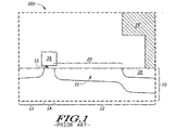
図1は、この技術において知られているような従来の電界効果トランジスタ100の一部分を示す。半導体基板10はチャンネル領域14によって分離されたドレイン領域12とソース領域13を備えており、これにより電界効果トランジスタの一部分を形成している。この技術において周知のように、半導体基板10は、シリコン層または他の半導体材料の層で構成することができる。一例として、シリコン層は、エピタキシャルプロセスを用いて成長される結晶性シリコンで実質的に構成することができる。
FIG. 1 shows a portion of a conventional
更に図1を参照すると、ゲート電極16はゲート酸化膜15およびチャンネル領域14の上にある。チャンネル領域14を横切って流れる電流は、ゲート電極16に加える電圧を制御することによって操作することができる。ドレイン領域12は、第1部分18と第2部分20とからなっている。第2部分20は、ドリフト領域22を有し、第1部分18よりも軽度にドープされている。チャンネル領域14は第2部分20に隣接している。ドレイン電極24はドレイン領域12の第1部分18の上にある。
Still referring to FIG. 1, the
回路デバイスの寸法が益々小さくなると、ソースとドレインとの間の電界はそれに対応して増加する。その結果、電荷キャリアが、ホットキャリア注入またはHCIとして知られる現象で、デバイスのゲート酸化膜に注入される可能性が増大する。もしそれが対処されないままになっていると、HCIは、場合によっては、回路故障を含む回路性能の著しい低下につながることがある。回路デバイスのサイズ減少のもう一つの結果は、そのような回路デバイス間の寄生容量の増加であり、これもまた著しい性能低下につながることがある。 As circuit device dimensions become smaller and smaller, the electric field between the source and drain increases correspondingly. As a result, charge carriers are more likely to be injected into the gate oxide of the device, a phenomenon known as hot carrier injection or HCI. If left unaccounted for, HCI can in some cases lead to significant degradation of circuit performance, including circuit failures. Another result of circuit device size reduction is an increase in parasitic capacitance between such circuit devices, which can also lead to significant performance degradation.
これらおよびその他の問題は、ファラデーシールドやフィールドプレートなどの、この技術において周知となっている種々の技術によって対処されてきた。しかしながら、前節で述べたように、ファラデーシールドは、寄生容量を減らす効果があるが、HCIを減らすように電界を減らす有益な効果がほとんどなく、また、ピーク電界を減らすのに適合したフィールドプレートは寄生容量を増やす傾向にある。つまり、現在の解決策は、別の問題を生じるか悪化させる犠牲のもとに、一つの問題を解決する傾向がある。 These and other problems have been addressed by various techniques well known in the art, such as Faraday shields and field plates. However, as mentioned in the previous section, the Faraday shield has the effect of reducing the parasitic capacitance, but has little beneficial effect of reducing the electric field so as to reduce the HCI, and the field plate suitable for reducing the peak electric field is It tends to increase parasitic capacitance. In other words, current solutions tend to solve one problem at the expense of creating or exacerbating another problem.
従来技術のこれらおよび他の欠点を克服するために、図2に示すように、電界効果トランジスタ200内にシールド構造30が設けられる。シールド構造30の少なくとも一部分は、ドレイン領域12の第2部分20の上にある。導電性のシールド構造30は、半導体基板10から第1距離33にある第1部分32と、半導体10から第2距離35にある第2部分34からなっている。
To overcome these and other shortcomings of the prior art, a
図2に示す実施態様において、第1部分32と第2部分34とは互いに分離されていて、二つの別個のピースを形成している。シールド構造30は、一部分が電気絶縁性誘電スタック300の上にあり、他の部分がその内部にある。電気絶縁性誘電スタック300は、誘電層310,320で構成されている。誘電層310の厚さが第1距離33を規定し、誘電層310,320の組み合せた厚さと、図2に示す実施態様においては、第1部分32とが、第2距離35を規定する。誘電層310,320は、同じ厚さを有してもよい
し、または異なる厚さを有してもよい。従って、第2距離35は第1距離33よりも大きい。一つの実施態様において、シールド構造30の第1部分32はドレイン領域12の第2部分20の上にあり、シールド構造30の第2部分34はゲート電極16と第1部分32の上にある。以下により詳しく説明するように、特定の実施態様においては、ドレイン電極24は、シールド構造30の第1部分32よりも第2部分34の近くに位置する。この配置は、前に述べたように、Cgdの最適な低減を可能にする。シールド構造30は、導電性固体プレートで構成してもよいし、あるいは、導電ストリップのグリッド配列または他の配列で構成してもよい。シールド構造30は、例えば、タングステンシリサイドなどの金属で構成してもよいし、あるいは、他の金属、または、ドープされた半導体材料などの他の導電性材料で構成してもよい。当業者にとって容易に明らかとなるであろうように、他の適切な材料を使用することもできる。
In the embodiment shown in FIG. 2, the
第1距離33は、第1部分32が半導体基板10に対して十分近くにあるように選択されることにより、ドリフト領域22内の水平および垂直電界成分が、電界効果トランジスタ200の動作中に実質的に変えられ、それにより、HCIを減らすことができる。HCIの減少はデバイスのドリフトを減少させる。第1距離33はまた、第1部分32が半導体基板10に対して十分近くにあるように選択されるので、ゲート電極16とドレイン電極24との間の破壊電圧(BV)を、他のパラメータに否定的な影響を与えることなしに、大きくすることができる。第2部分34の機能はCgdを減らすことであるので、第2距離35は、前に述べたように、第1距離33よりも大きい。特定の実施態様において、第2距離35は第1距離33よりも約3倍から4倍大きい。例えば、一つの実施態様において、第1距離33を約200ナノメータとし、第2距離35を約600から800ナノメータとすることができる。他のデバイス配置は異なる距離値を有するものであってもよい。第1距離33および第2距離35は、半導体基板10の表面から出発し、そこから離れて垂直に延びる方向に沿って測定される。第2部分34をゲート電極16から隔てる最短直線距離は、第1距離33よりも大きく、一つの実施態様においては、第2距離35よりも小さい。図に明確に示されていないこの最短直線距離を第3距離と呼ぶ。シールド構造30は第1高さ41を有し、ドレイン電極24は第2高さ43を有する。第1高さ41は第2高さ43よりも小さい。
The
更に図2において、二重シールド構造の特定の実施態様において、シールド構造30の第2部分34は、完全にまたは部分的にゲート電極16の上にあり、少なくとも部分的に第1部分32の上にあるようにゲート電極16を越えて延びている。第2部分34のオプションとしての破線部分31によって示すように、第2部分34は、ドレイン電極24が第1部分32よりも第2部分に近くなるように、第1部分32を越えてドレイン電極24に向かって延びることもできる。図2に示す実施態様において、ゲート電極16、ドレイン電極24、およびシールド構造30はそれぞれ、半導体基板10の表面11の上にある。
Still referring to FIG. 2, in a particular embodiment of the double shield structure, the
シールド構造30は、第1部分32と第2部分34とを含む別個の部分で構成することができる。より詳しくは、シールド構造30の第1部分32と第2部分34とを物理的に分離することができ、それによりFETデバイスの別個のピースを構成することができる。第1部分を第2部分から物理的に分離することにより、FETの機能を最適にするように計算された方法で各部分を独立に配置するという柔軟性を与えることができる。一方、別の実施態様において、シールド構造30は、第1部分32と第2部分34とが互いに結合された単一部分で構成することもできる。この実施態様は、HCIとCgsの減少といった、物理的に分離された実施態様の利点の少なくともいくつかを提供するが、設計上の柔軟性の程度は小さくなる。例えば、第1部分32と第2部分34とを互いに結合した場合、それらの部分に独立してバイアスをかけることはできなくなる。シールド構造30のバイアスはあとで更に十分に説明する。本発明のこの説明において、第1部分32と第2
部分34とからなるシールド構造30は、それらの部分が結合されているか分離されているかにかかわらず、「二重シールド」構成と呼ばれる。
The
A
いくつかの応用に対して、シールド構造30は電気的にバイアスされなくてもよい。他の応用に対して、シールド構造30をバイアスすることが望ましいことがあり得る。シールド構造30の第1部分32及び第2部分34は、一つの実施態様において、大地電位に電気的に接続される。別の実施態様において、第1部分32および第2部分34は異なる電位に別々にバイアスされる。このことは、例えば、低いオン抵抗が望ましい場合に、重要になり得る。一般に、低いオン抵抗を達成するためには、閾値電圧が高いほど、第1部分32のバイアスを高くしなければならない。特定の実施態様において、第1部分32は、FETのための閾値電圧にほぼ等しい所定電位に電気的に接続され、第2部分34は、大地電位に電気的に接続される。
For some applications, the
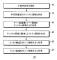
二重シールド構成は、既存のプロセスステップを僅かに変更するだけで生成することができる。図3は、本発明の一実施態様に従って二重シールド構成を有するFETの特定の実施態様を製造する方法40を示す。方法40の第1ステップ42は半導体基板を提供する。任意で選択されるステップである方法40の第2ステップ44は、半導体基板内チャンネル領域を形成することができる。方法40の第3ステップ46は、ゲート誘電層とゲート電極をチャンネル領域の上に形成する。方法40の第4ステップ48は、チャンネル領域に隣接した半導体基板内ドレイン領域を形成するようになっている。ここで、ドレイン領域は第1部分および第2部分を有し、第2部分は第1部分よりも軽度にドープされる。方法40の第5ステップ50において、導電性シールド構造はドレイン領域の第2部分の上に形成される。このシールド構造は、半導体基板から第1距離にある第1部分と、第1距離より大きい半導体基板からの第2距離にある第2部分とを有している。方法40の第6ステップ52は、ドレイン電極をドレイン領域の第1部分の上に形成するようになっている。方法40において示すように、ドレイン電極とシールド構造は異なるステップの間に形成される。方法40の他の実施態様において、導電性シールド構造は、ドレイン電極の形成の前か後、またはドレイン電極の形成と同時に形成することができる。
A double shield configuration can be created with only minor changes to existing process steps. FIG. 3 illustrates a
図4は、方法40の第5ステップにおいて形成される導電性シールド構造を形成する方法60を示す。方法60の第1ステップ62は、第1誘電層を半導体基板とゲート電極の上に形成するようになっている。この技術において周知のように、誘電層の形成は、従来、標準的な処理技術に従って、誘電材料の成膜とパターンニング、不要部分のエッチング、誘電材料の平坦化、および他のステップを含むことができる。方法60によって形成される誘電層は酸化物層または窒化物層であってもよく、いくつかの他の誘電材料で構成されてもよい。例えば、酸化物層は、酸化炉の中で熱で成長されるか、化学気相堆積プロセスによって堆積される二酸化シリコンで実質的に構成することができる。他の例としては、酸化物層は、化学蒸着堆積プロセスによって堆積されるテトラ・エチル・オルト・シリケート(TEOS)または燐酸シリケートガラスかで実質的に構成するか、あるいは、化学蒸着堆積プロセスによっても堆積される酸窒化シリコンで実質的に構成することができる。また、酸化物層は、例えば、酸化ハフニウムなどの高誘電率材料で構成することができる。窒化物層は、一例として、化学蒸着堆積プロセスによって堆積される窒化シリコンで実質的に構成することができる。もう一つの例として、窒化物層は、化学蒸着堆積プロセスによっても堆積される酸窒化シリコンで実質的に構成することができる。
FIG. 4 shows a
更に図4において、方法60の第2ステップ64は、シールド構造の第1部分を第1誘電層の上に形成する。方法60の第3ステップ66は、第2誘電層をシールド構造の第1部分の上に形成する。方法60の第4ステップ68において、シールド構造の第2部分が第2誘電層の上に形成される。方法60は、第3誘電層がシールド構造の第2部分の上に形成される、任意で選択される第5ステップ70を含むことができる。
Still referring to FIG. 4, a
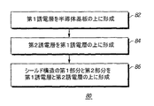
別の実施態様においては、図5に示すように、方法60は、第1誘電層が半導体基板の上に形成される第1ステップ82を有する方法80と置き換えることができる。方法80の第2ステップ84は、第2誘電層を第1誘電層の上に形成する。方法80の第3ステップ86は、導電性シールド構造の第1部分と第2部分を第1誘電層と第2誘電層の上に形成する。方法80は二重シールド構造の一実施態様を形成する。この実施態様においては、第1部分と第2部分が、図6に示すように、互いに物理的に接続されて、連続または単一構造を形成する。
In another embodiment, as shown in FIG. 5,
いま図6において、二重シールド構成の一実施態様が示されており、ここでは、シールド構造30の第1部分32および第2部分34は互いに接続されて単一構造を形成している。表面11の近くにあると同時にゲート電極16から離間されているようなシールド構造の必要性は本書にすでに述べられている。図6の単一構造実施態様において、この必要性は、厚い相互誘電層(ILD)88を、ドリフト領域22およびドレイン領域12の上の第1ピース90と、ソース領域13およびチャンネル領域14の上の第2ピース92に分けることによって達成される。これは、厚いILD88を堆積した後、厚いILD88を第1ピース90と第2ピース92の間の領域から除去するように、厚いILD88の一部分をマスキングしエッチングすることによって達成することもできる。図5に関連して説明したように、その後、薄いILDを厚いILD88の上部に堆積させる。シールド構造30は厚いILD88および薄いILD94の上に形成される。この実施態様は、所望なように、シールド構造30の第1部分32を表面11に適当に近づけて配置すると同時に、第2部分34をゲート電極16から適当に離して配置する。しかしながら、これは、第1部分32と第2部分34とを独立してバイアスできるようにはせず、また柔軟性の欠如の故に、一般的な構成に容易には適合しない。
Referring now to FIG. 6, one embodiment of a double shield configuration is shown where the
前に、FETの製造中に実現される二重プレート構造の特定の実施態様を説明した。説明したように、プレートの一部分は、ピーク電界に影響を与えるように半導体の十分近くに、しかし、Cgsを著しく増やさないようにゲートから十分離して、作成することができる。プレートの第2部分は、ゲートをドレインからシールドしてCgdを減らすように、厚い方の誘電層の上部に形成されるが、それでもなお、Cgsを著しく増やさないようにゲートから十分離して形成される。 Previously, specific embodiments of the dual plate structure realized during the fabrication of the FET have been described. As explained, a portion of the plate can be made close enough to the semiconductor to affect the peak electric field, but well separated from the gate so as not to significantly increase Cgs. The second part of the plate is formed on top of the thicker dielectric layer so as to shield the gate from the drain and reduce Cgd, but still be separated from the gate so as not to significantly increase Cgs. The
本発明は特定の実施態様に関して説明したが、本発明の精神と範囲から逸脱しなければ種々の変更が可能であることは当業者にとって明らかであろう。そのような変更の種々の例は前述の説明の中で示されている。従って、本発明の実施態様の開示は本発明の範囲を表すためのものであり、限定的なものではない。本発明の範囲は添付の特許請求の範囲によって要求される範囲だけに制限されるべきものである。例えば、ここで述べられた二重シールド構成は種々の実施態様で実現可能であること、および、これらの実施態様のいくつかについての前記議論は、すべての可能な実施態様の完全な説明を必ずしも表していないことは、当業者にとって容易に明らかとなるであろう。 Although the invention has been described with reference to specific embodiments, it will be apparent to those skilled in the art that various modifications can be made without departing from the spirit and scope of the invention. Various examples of such changes are shown in the foregoing description. Accordingly, the disclosure of embodiments of the invention is intended to represent the scope of the invention and is not limiting. The scope of the present invention should be limited only to the extent required by the appended claims. For example, the double shield configuration described herein can be implemented in various embodiments, and the above discussion of some of these embodiments does not necessarily provide a complete description of all possible embodiments. What is not represented will be readily apparent to those skilled in the art.
更に、利益と他の利点と問題の解決策とが特定の実施態様に関して説明されている。しかしながら、この利益と他の利点と問題の解決策、および、いずれかの利益、利点、または解決策を生じさせるか更に明確にする何らかの要素は、特許請求の範囲のいずれかまたはすべての、重要であるか、必要であるか、あるいは必須である特徴または要素と解釈されるものではない。 In addition, benefits, other advantages, and solutions to problems are described with respect to specific embodiments. However, this benefit and other advantages and solutions to problems, and any element that produces or further clarifies any benefit, advantage, or solution, are important for any or all of the claims. It is not to be construed as a feature or element that is necessary, necessary or essential.
また、用語「備える」、「含む」、「有する」、およびそのいずれの変形も、非排他的な包含をカバーするものではなく、多くの要素からなるプロセス、方法、物品、または装置は、それらの要素だけを含むのではなく、明確に述べられていない他の要素や、そのよ
うなプロセス、方法、物品、または装置に固有の他の要素を含むことができる。
Also, the terms “comprising”, “including”, “having”, and any variations thereof do not cover non-exclusive inclusions, and a process, method, article, or device consisting of many elements May include other elements not specifically stated, or other elements specific to such processes, methods, articles, or devices.
更に、ここに開示された実施態様と制限は、もしその実施態様と制限またはそのいずれかが、(1)特許請求の範囲において明確に請求されていなく、かつ、(2)均等物の原義のもとに、特許請求の範囲の中の明示された要素および制限またはそのいずれかの均等物であるか潜在的に均等物であるならば、開放の原義のもとに公衆に開放されない。 Further, the embodiments and limitations disclosed herein are not intended to limit the embodiments and / or limitations thereof, either (1) not explicitly claimed in the claims, and (2) the original equivalents. Basically, any explicit elements and limitations in the claims, or any equivalent or potential equivalent, will not be open to the public under the original principle of opening.
Claims (19)
前記半導体基板内にあって、かつ第1部分と、前記第1部分よりも軽度にドープされた第2部分とを有するドレイン領域と、
前記半導体基板内にあって、前記ドレイン領域の前記第2部分に隣接したチャンネル領域と、
前記チャンネル領域の上にあるゲート電極と、
前記ドレイン領域の前記第1部分の上にあるドレイン電極と、
前記ドレイン領域の前記第2部分の上にあって、前記半導体基板から第1距離にある第1部分を有すると共に、前記半導体基板から第2距離にある第2部分を有し、前記第2距離が前記第1距離よりも大きい導電性シールド構造と、
を備えることを特徴とする電界効果トランジスタ。 A semiconductor substrate;
A drain region in the semiconductor substrate and having a first portion and a second portion lightly doped than the first portion;
A channel region in the semiconductor substrate and adjacent to the second portion of the drain region;
A gate electrode overlying the channel region;
A drain electrode overlying the first portion of the drain region;
Having a first portion over the second portion of the drain region at a first distance from the semiconductor substrate and having a second portion at a second distance from the semiconductor substrate; A conductive shield structure having a larger than the first distance;
A field effect transistor comprising:
前記導電性シールド構造の前記第2部分は、大地電位に電気的に接続されることを特徴とする請求項8に記載の電界効果トランジスタ。 The first portion of the conductive shield structure is electrically connected to a predetermined potential approximately equal to a threshold voltage for the field effect transistor; and
9. The field effect transistor according to claim 8, wherein the second portion of the conductive shield structure is electrically connected to a ground potential.
前記ドレイン電極は第2厚さを有し、
前記第1厚さは前記第2厚さよりも小さいことを特徴とする請求項1に記載の電界効果トランジスタ。 The conductive shield structure has a first thickness;
The drain electrode has a second thickness;
The field effect transistor according to claim 1, wherein the first thickness is smaller than the second thickness.
前記半導体基板内にあって、第1部分と、前記第1部分よりも軽度にドープされた第2部分とを有するドレイン領域と、
前記半導体基板内にあって、前記ドレイン領域の前記第2部分に隣接したチャンネル領
域と、
前記半導体基板の前記表面の上と前記チャンネル領域の上にあるゲート電極と、
前記半導体基板の前記表面の上と前記ドレイン領域の前記第1部分の上に位置するドレイン電極と、
第1部分および第2部分を有する導電性シールド構造とを備え、
前記導電性シールド構造の前記第1部分は前記ドレイン領域の前記第2部分の上にあり、
前記導電性シールド構造の前記第1部分は前記半導体基板の前記表面から第1距離にあり、
前記導電性シールド構造の前記第2部分は前記ゲート電極の上にあり、
前記導電性シールド構造の前記第2部分は前記半導体基板の前記表面から第2距離にあり、
前記第1距離は前記第2距離よりも小さい、ことを特徴とする電界効果トランジスタ。 A semiconductor substrate having a surface;
A drain region in the semiconductor substrate having a first portion and a second portion lightly doped than the first portion;
A channel region in the semiconductor substrate and adjacent to the second portion of the drain region;
A gate electrode over the surface of the semiconductor substrate and over the channel region;
A drain electrode located on the surface of the semiconductor substrate and on the first portion of the drain region;
A conductive shield structure having a first portion and a second portion;
The first portion of the conductive shield structure is over the second portion of the drain region;
The first portion of the conductive shield structure is at a first distance from the surface of the semiconductor substrate;
The second portion of the conductive shield structure is over the gate electrode;
The second portion of the conductive shield structure is at a second distance from the surface of the semiconductor substrate;
The field effect transistor according to claim 1, wherein the first distance is smaller than the second distance.
前記導電性シールド構造の前記第2部分は、大地電位に電気的に接続される、ことを特徴とする請求項11に記載の電界効果トランジスタ。 The first portion of the conductive shield structure is electrically connected to a predetermined potential approximately equal to a threshold voltage for the field effect transistor; and
The field effect transistor according to claim 11, wherein the second portion of the conductive shield structure is electrically connected to a ground potential.
チャンネル領域を含む半導体基板を提供するステップと、
前記チャンネル領域の上にゲート電極を形成するステップと、
前記半導体基板内にあって、第1部分と、前記第1部分よりも軽度にドープされ、前記チャンネル領域に隣接した第2部分とを有するドレイン領域を形成するステップと、
前記半導体基板から第1距離にある第1部分を有すると共に、前記半導体基板から第2距離にある第2部分を有し、前記第2距離が前記第1距離よりも大きい導電性シールド構造を、前記ドレイン領域の前記第2部分の上に形成するステップと、
前記ドレイン領域の前記第1部分の上にドレイン電極を形成するステップとを備えることを特徴とする方法。 A method of manufacturing a field effect transistor comprising:
Providing a semiconductor substrate including a channel region;
Forming a gate electrode on the channel region;
Forming a drain region in the semiconductor substrate having a first portion and a second portion lightly doped than the first portion and adjacent to the channel region;
A conductive shield structure having a first portion at a first distance from the semiconductor substrate and a second portion at a second distance from the semiconductor substrate, wherein the second distance is greater than the first distance; Forming on the second portion of the drain region;
Forming a drain electrode on the first portion of the drain region.
前記半導体基板の上に第1誘電層を形成するステップと、
前記第1誘電層の上に前記導電性シールド構造の前記第1部分を形成するステップと、
前記導電性シールド構造の前記第1部分の上に第2誘電層を形成するステップと、
前記第2誘電層の上に前記導電性シールド構造の前記第2部分を形成するステップとを更に備えることを特徴とする請求項16に記載の方法。 Forming the conductive shield structure comprises:
Forming a first dielectric layer on the semiconductor substrate;
Forming the first portion of the conductive shield structure on the first dielectric layer;
Forming a second dielectric layer on the first portion of the conductive shield structure;
The method of claim 16, further comprising: forming the second portion of the conductive shield structure on the second dielectric layer.
前記半導体基板の上に第1誘電層を形成するステップと、
前記第1誘電層の上に第2誘電層を形成するステップと、
前記第1誘電層および第2誘電層の上に前記導電性シールド構造の前記第1部分および
第2部分を形成するステップとを更に備えることを特徴とする請求項16に記載の方法。 Forming the conductive shield structure comprises:
Forming a first dielectric layer on the semiconductor substrate;
Forming a second dielectric layer on the first dielectric layer;
The method of claim 16, further comprising forming the first and second portions of the conductive shield structure over the first and second dielectric layers.
前記第2誘電層を形成するステップは、第1厚さよりも少ない第2厚さを有する第2誘電層を形成するステップを更に備えることを特徴とする請求項18に記載の方法。 Forming the first dielectric layer further comprises forming a first dielectric layer having a first thickness; and
The method of claim 18, wherein forming the second dielectric layer further comprises forming a second dielectric layer having a second thickness that is less than the first thickness.
Applications Claiming Priority (2)
| Application Number | Priority Date | Filing Date | Title |
|---|---|---|---|
| US10/209,816 US6870219B2 (en) | 2002-07-31 | 2002-07-31 | Field effect transistor and method of manufacturing same |
| PCT/US2003/018938 WO2004012270A2 (en) | 2002-07-31 | 2003-06-16 | Field effect transistor and method of manufacturing same |
Publications (2)
| Publication Number | Publication Date |
|---|---|
| JP2005535113A true JP2005535113A (en) | 2005-11-17 |
| JP2005535113A5 JP2005535113A5 (en) | 2006-08-10 |
Family
ID=31187146
Family Applications (1)
| Application Number | Title | Priority Date | Filing Date |
|---|---|---|---|
| JP2004524517A Pending JP2005535113A (en) | 2002-07-31 | 2003-06-16 | Field effect transistor and manufacturing method thereof |
Country Status (7)
| Country | Link |
|---|---|
| US (1) | US6870219B2 (en) |
| EP (1) | EP1525622A2 (en) |
| JP (1) | JP2005535113A (en) |
| CN (1) | CN1672263A (en) |
| AU (1) | AU2003281740A1 (en) |
| TW (1) | TWI311813B (en) |
| WO (1) | WO2004012270A2 (en) |
Cited By (5)
| Publication number | Priority date | Publication date | Assignee | Title |
|---|---|---|---|---|
| JP2007537596A (en) * | 2004-05-13 | 2007-12-20 | クリー インコーポレイテッド | Wide band gap field effect transistor having a source region connected to a field plate |
| JP2009164651A (en) * | 2009-04-24 | 2009-07-23 | Sanyo Electric Co Ltd | Semiconductor apparatus |
| US8933486B2 (en) | 2006-11-13 | 2015-01-13 | Cree, Inc. | GaN based HEMTs with buried field plates |
| US9755059B2 (en) | 2013-06-09 | 2017-09-05 | Cree, Inc. | Cascode structures with GaN cap layers |
| US11791385B2 (en) | 2005-03-11 | 2023-10-17 | Wolfspeed, Inc. | Wide bandgap transistors with gate-source field plates |
Families Citing this family (17)
| Publication number | Priority date | Publication date | Assignee | Title |
|---|---|---|---|---|
| CN100546032C (en) * | 2003-04-22 | 2009-09-30 | Dsp集团瑞士股份公司 | The semiconductor device and the method for operation thereof that comprise field-effect transistor |
| JP2007503717A (en) * | 2003-08-27 | 2007-02-22 | コーニンクレッカ フィリップス エレクトロニクス エヌ ヴィ | Electronic device having LDMOS transistor |
| US7501669B2 (en) | 2003-09-09 | 2009-03-10 | Cree, Inc. | Wide bandgap transistor devices with field plates |
| WO2005069378A2 (en) | 2004-01-10 | 2005-07-28 | Hvvi Semiconductors, Inc. | Power semiconductor device and method therefor |
| EP1635399B1 (en) * | 2004-09-08 | 2011-05-04 | STMicroelectronics Srl | Lateral MOS device and method of making the same |
| US8530963B2 (en) | 2005-01-06 | 2013-09-10 | Estivation Properties Llc | Power semiconductor device and method therefor |
| US8564057B1 (en) * | 2007-01-09 | 2013-10-22 | Maxpower Semiconductor, Inc. | Power devices, structures, components, and methods using lateral drift, fixed net charge, and shield |
| US8253198B2 (en) * | 2009-07-30 | 2012-08-28 | Micron Technology | Devices for shielding a signal line over an active region |
| CN102237276B (en) * | 2010-04-22 | 2014-04-16 | 上海华虹宏力半导体制造有限公司 | Method for manufacturing radio frequency LDMOS (Laterally Diffused Metal Oxide Semiconductor) device |
| EP2383786B1 (en) * | 2010-04-29 | 2018-08-15 | Ampleon Netherlands B.V. | Semiconductor transistor comprising two electrically conductive shield elements |
| JP2011249728A (en) * | 2010-05-31 | 2011-12-08 | Toshiba Corp | Semiconductor device and method for manufacturing the same |
| US20120175679A1 (en) * | 2011-01-10 | 2012-07-12 | Fabio Alessio Marino | Single structure cascode device |
| JP5776217B2 (en) * | 2011-02-24 | 2015-09-09 | 富士通株式会社 | Compound semiconductor device |
| US8680615B2 (en) | 2011-12-13 | 2014-03-25 | Freescale Semiconductor, Inc. | Customized shield plate for a field effect transistor |
| US9679981B2 (en) | 2013-06-09 | 2017-06-13 | Cree, Inc. | Cascode structures for GaN HEMTs |
| JP6242118B2 (en) * | 2013-08-29 | 2017-12-06 | オリンパス株式会社 | Switch circuit, sample hold circuit, and solid-state imaging device |
| US9853145B1 (en) * | 2016-10-04 | 2017-12-26 | Vanguard International Semiconductor Corporation | High-voltage semiconductor device and method of manufacturing the same |
Family Cites Families (11)
| Publication number | Priority date | Publication date | Assignee | Title |
|---|---|---|---|---|
| JPS56169369A (en) * | 1980-05-30 | 1981-12-26 | Sharp Corp | High withstand voltage mos field effect semiconductor device |
| JPS56169368A (en) * | 1980-05-30 | 1981-12-26 | Sharp Corp | High withstand voltage mos field effect semiconductor device |
| JPS58137256A (en) | 1982-02-10 | 1983-08-15 | Hitachi Ltd | Insulated gate semiconductor device |
| US5119149A (en) * | 1990-10-22 | 1992-06-02 | Motorola, Inc. | Gate-drain shield reduces gate to drain capacitance |
| US5252848A (en) * | 1992-02-03 | 1993-10-12 | Motorola, Inc. | Low on resistance field effect transistor |
| US5898198A (en) * | 1997-08-04 | 1999-04-27 | Spectrian | RF power device having voltage controlled linearity |
| US5912490A (en) * | 1997-08-04 | 1999-06-15 | Spectrian | MOSFET having buried shield plate for reduced gate/drain capacitance |
| US6001710A (en) * | 1998-03-30 | 1999-12-14 | Spectrian, Inc. | MOSFET device having recessed gate-drain shield and method |
| US6222229B1 (en) | 1999-02-18 | 2001-04-24 | Cree, Inc. | Self-aligned shield structure for realizing high frequency power MOSFET devices with improved reliability |
| KR100282426B1 (en) * | 1999-03-17 | 2001-02-15 | 김영환 | Smart power device and method for fabricating the same |
| KR100302611B1 (en) * | 1999-06-07 | 2001-10-29 | 김영환 | High power semiconductor device and fabrication method thereof |
-
2002
- 2002-07-31 US US10/209,816 patent/US6870219B2/en not_active Expired - Lifetime
-
2003
- 2003-06-16 WO PCT/US2003/018938 patent/WO2004012270A2/en active Application Filing
- 2003-06-16 CN CN03817910.5A patent/CN1672263A/en active Pending
- 2003-06-16 AU AU2003281740A patent/AU2003281740A1/en not_active Abandoned
- 2003-06-16 JP JP2004524517A patent/JP2005535113A/en active Pending
- 2003-06-16 EP EP03742012A patent/EP1525622A2/en not_active Withdrawn
- 2003-07-10 TW TW092118872A patent/TWI311813B/en active
Non-Patent Citations (1)
| Title |
|---|
| JPN6010001807, N.Fujishima et al., "A 700V Lateral Power MOSFET with Narrow Gap Double Metal Field Plates Realizing Low On−resistance an", Proceeding of the 13th International Symposium on Power Semiconductor Devices & ICs, 2001, P.255−258 * |
Cited By (6)
| Publication number | Priority date | Publication date | Assignee | Title |
|---|---|---|---|---|
| JP2007537596A (en) * | 2004-05-13 | 2007-12-20 | クリー インコーポレイテッド | Wide band gap field effect transistor having a source region connected to a field plate |
| US9773877B2 (en) | 2004-05-13 | 2017-09-26 | Cree, Inc. | Wide bandgap field effect transistors with source connected field plates |
| US11791385B2 (en) | 2005-03-11 | 2023-10-17 | Wolfspeed, Inc. | Wide bandgap transistors with gate-source field plates |
| US8933486B2 (en) | 2006-11-13 | 2015-01-13 | Cree, Inc. | GaN based HEMTs with buried field plates |
| JP2009164651A (en) * | 2009-04-24 | 2009-07-23 | Sanyo Electric Co Ltd | Semiconductor apparatus |
| US9755059B2 (en) | 2013-06-09 | 2017-09-05 | Cree, Inc. | Cascode structures with GaN cap layers |
Also Published As
| Publication number | Publication date |
|---|---|
| EP1525622A2 (en) | 2005-04-27 |
| TWI311813B (en) | 2009-07-01 |
| US6870219B2 (en) | 2005-03-22 |
| US20040021175A1 (en) | 2004-02-05 |
| WO2004012270A3 (en) | 2004-04-15 |
| TW200409359A (en) | 2004-06-01 |
| CN1672263A (en) | 2005-09-21 |
| AU2003281740A1 (en) | 2004-02-16 |
| WO2004012270A2 (en) | 2004-02-05 |
Similar Documents
| Publication | Publication Date | Title |
|---|---|---|
| JP2005535113A (en) | Field effect transistor and manufacturing method thereof | |
| US10084037B2 (en) | MOSFET active area and edge termination area charge balance | |
| TWI325175B (en) | Metal-oxide-semiconductor device including a buried lightly-doped drain region | |
| US7105934B2 (en) | FinFET with low gate capacitance and low extrinsic resistance | |
| KR100719301B1 (en) | Lateral thin-film silicon-on-insulator soi device having a gate electrode and a field plate electrode | |
| US8865549B2 (en) | Recessed channel insulated-gate field effect transistor with self-aligned gate and increased channel length | |
| US8981460B2 (en) | Power semiconductor field effect transistor structure with charge trapping material in the gate dielectric | |
| KR101267293B1 (en) | Power semiconductor device having improved performance and method | |
| US20060249785A1 (en) | Power MOSFET device structure for high frequency applications | |
| US20210175336A1 (en) | Lateral double-diffused transistor and manufacturing method thereof | |
| US20090267145A1 (en) | Mosfet device having dual interlevel dielectric thickness and method of making same | |
| TW201401521A (en) | Lateral transistor and method for manufacturing the same | |
| US7224021B2 (en) | MOSFET with high angle sidewall gate and contacts for reduced miller capacitance | |
| US8216908B2 (en) | Extended drain transistor and method of manufacturing the same | |
| KR20190142881A (en) | Integrated circuit device | |
| US20060170053A1 (en) | Accumulation mode multiple gate transistor | |
| US20090166731A1 (en) | Vertical-type field-effect transistor and manufacturing method thereof | |
| US7838371B2 (en) | Method of manufacturing a FET gate | |
| KR100734143B1 (en) | Double-diffused metal oxide semiconductor and method for fabricating the same | |
| KR100975792B1 (en) | Field effect transistor and method of manufacturing same | |
| CN113035948B (en) | Power device, power electronic equipment and manufacturing method of power device | |
| TWI704606B (en) | Trench power semiconductor device and manufacturing method thereof | |
| US7994414B2 (en) | Semiconductor device | |
| US6153909A (en) | Semiconductor device and method for fabricating the same | |
| TW202322390A (en) | Semiconductor device and fabrication method thereof |
Legal Events
| Date | Code | Title | Description |
|---|---|---|---|
| A521 | Written amendment |
Free format text: JAPANESE INTERMEDIATE CODE: A523 Effective date: 20060616 |
|
| A621 | Written request for application examination |
Free format text: JAPANESE INTERMEDIATE CODE: A621 Effective date: 20060616 |
|
| A977 | Report on retrieval |
Free format text: JAPANESE INTERMEDIATE CODE: A971007 Effective date: 20080826 |
|
| A131 | Notification of reasons for refusal |
Free format text: JAPANESE INTERMEDIATE CODE: A131 Effective date: 20100119 |
|
| A02 | Decision of refusal |
Free format text: JAPANESE INTERMEDIATE CODE: A02 Effective date: 20100622 |