JP2005303746A - Imaging apparatus - Google Patents
Imaging apparatus Download PDFInfo
- Publication number
- JP2005303746A JP2005303746A JP2004118337A JP2004118337A JP2005303746A JP 2005303746 A JP2005303746 A JP 2005303746A JP 2004118337 A JP2004118337 A JP 2004118337A JP 2004118337 A JP2004118337 A JP 2004118337A JP 2005303746 A JP2005303746 A JP 2005303746A
- Authority
- JP
- Japan
- Prior art keywords
- voltage
- output
- unit cell
- unit
- read voltage
- Prior art date
- Legal status (The legal status is an assumption and is not a legal conclusion. Google has not performed a legal analysis and makes no representation as to the accuracy of the status listed.)
- Pending
Links
Images


Classifications
-
- H—ELECTRICITY
- H04—ELECTRIC COMMUNICATION TECHNIQUE
- H04N—PICTORIAL COMMUNICATION, e.g. TELEVISION
- H04N23/00—Cameras or camera modules comprising electronic image sensors; Control thereof
- H04N23/70—Circuitry for compensating brightness variation in the scene
-
- A—HUMAN NECESSITIES
- A01—AGRICULTURE; FORESTRY; ANIMAL HUSBANDRY; HUNTING; TRAPPING; FISHING
- A01B—SOIL WORKING IN AGRICULTURE OR FORESTRY; PARTS, DETAILS, OR ACCESSORIES OF AGRICULTURAL MACHINES OR IMPLEMENTS, IN GENERAL
- A01B13/00—Ploughs or like machines for special purposes ; Ditch diggers, trench ploughs, forestry ploughs, ploughs for land or marsh reclamation
- A01B13/08—Ploughs or like machines for special purposes ; Ditch diggers, trench ploughs, forestry ploughs, ploughs for land or marsh reclamation for working subsoil
-
- A—HUMAN NECESSITIES
- A01—AGRICULTURE; FORESTRY; ANIMAL HUSBANDRY; HUNTING; TRAPPING; FISHING
- A01B—SOIL WORKING IN AGRICULTURE OR FORESTRY; PARTS, DETAILS, OR ACCESSORIES OF AGRICULTURAL MACHINES OR IMPLEMENTS, IN GENERAL
- A01B27/00—Clod-crushers
-
- A—HUMAN NECESSITIES
- A01—AGRICULTURE; FORESTRY; ANIMAL HUSBANDRY; HUNTING; TRAPPING; FISHING
- A01B—SOIL WORKING IN AGRICULTURE OR FORESTRY; PARTS, DETAILS, OR ACCESSORIES OF AGRICULTURAL MACHINES OR IMPLEMENTS, IN GENERAL
- A01B59/00—Devices specially adapted for connection between animals or tractors and agricultural machines or implements
- A01B59/04—Devices specially adapted for connection between animals or tractors and agricultural machines or implements for machines pulled or pushed by a tractor
- A01B59/042—Devices specially adapted for connection between animals or tractors and agricultural machines or implements for machines pulled or pushed by a tractor having pulling means arranged on the rear part of the tractor
-
- H—ELECTRICITY
- H04—ELECTRIC COMMUNICATION TECHNIQUE
- H04N—PICTORIAL COMMUNICATION, e.g. TELEVISION
- H04N25/00—Circuitry of solid-state image sensors [SSIS]; Control thereof
- H04N25/60—Noise processing, e.g. detecting, correcting, reducing or removing noise
- H04N25/62—Detection or reduction of noise due to excess charges produced by the exposure, e.g. smear, blooming, ghost image, crosstalk or leakage between pixels
- H04N25/627—Detection or reduction of inverted contrast or eclipsing effects
Abstract
Description
本発明は、光を入射して光電変換する単位セルが、半導体基板上に1次元又は2次元に配置してなる撮像装置に関し、特に、強い光を入射したときに画像が黒つぶれする現象を防止するための技術に関する。 The present invention relates to an imaging device in which unit cells for photoelectric conversion upon incidence of light are arranged one-dimensionally or two-dimensionally on a semiconductor substrate, and in particular, a phenomenon that an image is blackened when strong light is incident. It relates to technology to prevent.
近年、家庭用ビデオカメラやデジタルスチルカメラなどの、撮像装置を用いた撮像機器が一般に普及している。
これらの撮像機器には、撮像装置として増幅型のイメージセンサを備えるものがある。
増幅型のイメージセンサには、雑音が低い等の優れた特徴がある反面、強い光を入射したときに画像が黒つぶれするという問題点がある。
In recent years, imaging devices using an imaging device such as a home video camera and a digital still camera have been widely used.
Some of these imaging devices include an amplification type image sensor as an imaging device.
The amplification type image sensor has excellent features such as low noise, but has a problem that the image is blacked out when strong light is incident.
特許文献1には、増幅型のイメージセンサであるCMOSイメージセンサの概要、及び上記と同様の問題点、及び、画素センサ毎に、リセット時の出力電圧に基づいて強い光の入射を検出して、リセット時の電圧を他の電圧と置き換えるCMOSイメージセンサが開示されており、当該問題点を防止することが可能であると記載されている。
特許文献1において、画像が黒つぶれする画素センサを検出する際の指標としているリセット時の出力電圧の変化は画像が黒つぶれする原因そものであり、たとえその変化量が僅かであっても、輝度情報に直接影響を及ぼすものである。
しかしながら、このリセット時の出力電圧の変化を検出するには、変化量が有る程度の大きさ以上にならなければ検出できないので、当該変化によって生じる悪影響を完全に除去することは困難である。
In
However, in order to detect the change in the output voltage at the time of resetting, the change cannot be detected unless the amount of change exceeds a certain level. Therefore, it is difficult to completely eliminate the adverse effects caused by the change.
また、強い光を入射したときのリセット時の出力電圧の変化の特性は急峻であり精度良く検出することが難しいので、黒つぶれを確実に防止することは容易でない。
例えば、特許文献1に開示されたCMOSイメージセンサで、中心部が十分に明るくその周辺部が徐々に暗くなるような物体を撮影すると、中心部の十分に明るい領域では黒つぶれを防止できるものの、その周辺部では黒つぶれが防止された領域との境界部分に近い明るいはずの部分が逆に暗くなってしまい、程度によってはリング状の黒つぶれが発生する。
In addition, since the characteristics of the change in the output voltage at the time of resetting when strong light is incident are steep and difficult to detect with high accuracy, it is not easy to reliably prevent blackout.
For example, in the CMOS image sensor disclosed in
そこで、本発明は、強い光を入射したときに画像が黒つぶれするという問題点を従来よりも確実に解決し、またリセット時の電圧の変化による悪影響を確実に排除することができる、撮像システム、撮像素子、信号処理装置、信号処理方法、及び信号処理プログラムを提供することを目的とする。 Accordingly, the present invention can solve the problem that an image is blacked out when a strong light is incident, more reliably than before, and can reliably eliminate an adverse effect due to a voltage change at reset. An image sensor, a signal processing device, a signal processing method, and a signal processing program are provided.
上記目的を達成するために、本発明に係る撮像システムは、撮像素子と信号処理装置とから構成され受光量に応じた輝度情報を後段の装置へ出力する撮像システムであって、撮像素子は、1画素に相当する光電変換部と初期化時の当該光電変換部の出力電圧に対応するリセット電圧及び受光量に応じた当該光電変換部の出力電圧に対応するリード電圧を生成し出力する出力部とを含む単位セルが1次元又は2次元状に複数個配列された撮像手段と、前記リセット電圧と前記リード電圧との差分に相当する差分電圧を前記単位セル毎に生成する差分電圧生成手段と、前記リード電圧と前記差分電圧とを信号処理装置へ単位セル毎に出力する素子出力手段とを備え、信号処理装置は、前記素子出力手段により単位セル毎に出力されたリード電圧がそれぞれ所定の範囲の電圧であるか否かに基づいて補正対象の単位セルを選定する選定手段と、前記素子出力手段により単位セル毎に出力された差分電圧のうちの前記補正対象の単位セル以外の単位セルに対応する差分電圧をそれぞれの単位セルに対応する輝度情報として後段の装置へ出力し高輝度を示す所定の電圧を前記補正対象の単位セルに対応するそれぞれの輝度情報として後段の装置へ出力するシステム出力手段とを備えることを特徴とする。 In order to achieve the above object, an imaging system according to the present invention is an imaging system that includes an imaging device and a signal processing device and outputs luminance information corresponding to the amount of received light to a subsequent device, and the imaging device includes: A photoelectric conversion unit corresponding to one pixel and an output unit that generates and outputs a reset voltage corresponding to the output voltage of the photoelectric conversion unit at initialization and a read voltage corresponding to the output voltage of the photoelectric conversion unit according to the amount of received light A plurality of unit cells including one-dimensional or two-dimensional array, and a differential voltage generating unit that generates a differential voltage corresponding to a difference between the reset voltage and the read voltage for each unit cell. Element output means for outputting the read voltage and the differential voltage to the signal processing device for each unit cell, and the signal processing device receives the read voltage output for each unit cell by the element output means. A selection unit that selects a unit cell to be corrected based on whether the voltage is within a predetermined range, and the unit to be corrected among the differential voltages output for each unit cell by the element output unit A differential voltage corresponding to a unit cell other than a cell is output as luminance information corresponding to each unit cell to a subsequent device, and a predetermined voltage indicating high luminance is output as subsequent luminance information corresponding to the unit cell to be corrected. System output means for outputting to the apparatus.
上記目的を達成するために、本発明に係る撮像素子は、1画素に相当する光電変換部と初期化時の当該光電変換部の出力電圧に対応するリセット電圧及び受光量に応じた当該光電変換部の出力電圧に対応するリード電圧を生成し出力する出力部とを含む単位セルが1次元又は2次元状に複数個配列された撮像手段と、前記リセット電圧と前記リード電圧との差分に相当する差分電圧を前記単位セル毎に生成する差分電圧生成手段と、前記リード電圧と前記差分電圧とを前記単位セル毎に出力する出力手段とを備えることを特徴とする。 In order to achieve the above object, the image sensor according to the present invention includes a photoelectric conversion unit corresponding to one pixel and a photoelectric conversion corresponding to a reset voltage corresponding to an output voltage of the photoelectric conversion unit at initialization and a received light amount. Equivalent to the difference between the reset voltage and the read voltage, and imaging means in which a plurality of unit cells including an output unit that generates and outputs a read voltage corresponding to the output voltage of the unit is arranged one-dimensionally or two-dimensionally Differential voltage generating means for generating a differential voltage for each unit cell; and output means for outputting the read voltage and the differential voltage for each unit cell.
上記目的を達成するために、本発明に係る信号処理装置は、初期化時の光電変換部の出力電圧に対応する単位セル毎のリセット電圧及び当該リセット電圧と受光量に応じた光電変換部の出力電圧に対応するリード電圧との差分に相当する単位セル毎の差分電圧を撮像素子から受け取って処理する信号処理装置であって、前記撮像素子から単位セル毎に出力されたリード電圧がそれぞれ所定の範囲の電圧であるか否かに基づいて補正対象の単位セルを選定する選定手段と、前記撮像素子からり単位セル毎に出力された差分電圧のうちの前記補正対象の単位セル以外の単位セルに対応する差分電圧をそれぞれの単位セルに対応する輝度情報として後段の装置へ出力し高輝度を示す所定の電圧を前記補正対象の単位セルに対応するそれぞれの輝度情報として後段の装置へ出力する出力手段とを備えることを特徴とする。 In order to achieve the above object, the signal processing apparatus according to the present invention includes a reset voltage for each unit cell corresponding to the output voltage of the photoelectric conversion unit at the time of initialization, and a photoelectric conversion unit corresponding to the reset voltage and the amount of received light. A signal processing apparatus that receives and processes a differential voltage for each unit cell corresponding to a difference from a read voltage corresponding to an output voltage from an image sensor, and each of the read voltages output from the image sensor for each unit cell is predetermined. A selection unit for selecting a unit cell to be corrected based on whether or not the voltage is in a range of a unit, and a unit other than the unit cell to be corrected among the differential voltages output for each unit cell from the image sensor The differential voltage corresponding to the cell is output as luminance information corresponding to each unit cell to the subsequent device, and a predetermined voltage indicating high luminance is output to each luminance information corresponding to the unit cell to be corrected. And an outputting means for outputting to the subsequent device as.
上記目的を達成するために、本発明に係る信号処理方法は、初期化時の光電変換部の出力電圧に対応する単位セル毎のリセット電圧及び当該リセット電圧と受光量に応じた光電変換部の出力電圧に対応するリード電圧との差分に相当する単位セル毎の差分電圧を撮像素子から受け取って処理する信号処理方法であって、前記撮像素子から単位セル毎に出力されたリード電圧がそれぞれ所定の範囲の電圧であるか否かに基づいて補正対象の単位セルを選定する選定ステップと、前記撮像素子から単位セル毎に出力された差分電圧のうちの前記補正対象の単位セル以外の単位セルに対応する差分電圧をそれぞれの単位セルに対応する輝度情報として後段の装置へ出力し高輝度を示す所定の電圧を前記補正対象の単位セルに対応するそれぞれの輝度情報として後段の装置へ出力する出力ステップとを含むことを特徴とする。 In order to achieve the above object, the signal processing method according to the present invention includes a reset voltage for each unit cell corresponding to the output voltage of the photoelectric conversion unit at the time of initialization, and a photoelectric conversion unit corresponding to the reset voltage and the amount of received light. A signal processing method for receiving a differential voltage for each unit cell corresponding to a difference from a read voltage corresponding to an output voltage from an image sensor, and processing the read voltage output from the image sensor for each unit cell. A selection step of selecting a unit cell to be corrected based on whether or not the voltage is in a range of a unit cell, and unit cells other than the unit cell to be corrected among the differential voltages output for each unit cell from the imaging device The difference voltage corresponding to each of the unit cells is output as luminance information corresponding to each unit cell to the subsequent device, and a predetermined voltage indicating high luminance is output to each luminance corresponding to the unit cell to be corrected. Characterized in that it comprises an output step of outputting to a downstream device as broadcast.
上記目的を達成するために、本発明に係る信号処理プログラムは、初期化時の光電変換部の出力電圧に対応する単位セル毎のリセット電圧及び当該リセット電圧と受光量に応じた光電変換部の出力電圧に対応するリード電圧との差分に相当する単位セル毎の差分電圧を撮像素子から受け取って処理する信号処理装置における信号処理プログラムであって、コンピュータに、前記撮像素子から単位セル毎に出力されたリード電圧がそれぞれ所定の範囲の電圧であるか否かに基づいて補正対象の単位セルを選定する選定ステップと、前記撮像素子から単位セル毎に出力された差分電圧のうちの前記補正対象の単位セル以外の単位セルに対応する差分電圧をそれぞれの単位セルに対応する輝度情報として後段の装置へ出力し高輝度を示す所定の電圧を前記補正対象の単位セルに対応するそれぞれの輝度情報として後段の装置へ出力する出力ステップとを実行させることを特徴とする。 In order to achieve the above object, a signal processing program according to the present invention includes a reset voltage for each unit cell corresponding to an output voltage of a photoelectric conversion unit at initialization, and a photoelectric conversion unit corresponding to the reset voltage and the amount of received light. A signal processing program in a signal processing apparatus that receives and processes a differential voltage for each unit cell corresponding to a difference from a read voltage corresponding to an output voltage from an image sensor, and outputs the signal to the computer for each unit cell from the image sensor A selection step of selecting a unit cell to be corrected based on whether or not each read voltage is a voltage within a predetermined range, and the correction target of the differential voltage output for each unit cell from the image sensor A differential voltage corresponding to a unit cell other than one unit cell is output as luminance information corresponding to each unit cell to a subsequent device and a predetermined voltage indicating high luminance Characterized in that to execute an output step of outputting to a downstream device as respective luminance information corresponding to the unit cell of the correction target.
課題を解決するための手段に記載した構成によって、リード時の電圧を画像が黒つぶれする画素センサを検出する際の指標として、黒つぶれが発生している可能性がある出力電圧を高輝度を示す電圧に置き換えることができるので、黒つぶれ等の原因であるリセット時の電圧の変化が生じる程度の入射光よりも充分弱い入射光から余裕をもって対策を施すことができる。 With the configuration described in the means for solving the problem, the output voltage that may be blacked out is set to a high luminance as an index when detecting a pixel sensor in which the voltage is read out. Since the voltage can be replaced with the voltage shown in the figure, it is possible to take a measure with a margin from incident light that is sufficiently weaker than incident light that causes a change in voltage at reset, which is a cause of blackout or the like.
従って、強い光を入射したときに画像が黒つぶれするという問題点を従来よりも確実に解決し、またリセット時の電圧の変化による悪影響を確実に排除することができる。
また、撮像システムにおいて、前記選定手段は、前記素子出力手段により単位セル毎に出力されたリード電圧がそれぞれ所定の範囲の電圧であるか否かを判断する判断手段と、前記素子出力手段により単位セル毎に出力された差分電圧に基づいて前記判断手段によりリード電圧が所定の範囲の電圧であると判断されなかったリード電圧に対応する単位セルの中から補正対象の単位セルを選択する選択手段とを含むことを特徴とすることもできる。
Therefore, it is possible to more reliably solve the problem that the image is blacked out when strong light is incident, and to reliably eliminate the adverse effects caused by the voltage change at the time of reset.
Further, in the imaging system, the selection unit includes a determination unit that determines whether the read voltage output for each unit cell by the element output unit is a voltage within a predetermined range, and the unit output unit. Selection means for selecting a unit cell to be corrected from among the unit cells corresponding to the read voltage whose read voltage is not determined to be in a predetermined range by the determination means based on the differential voltage output for each cell. It can also be characterized by including.
また、信号処理装置において、前記選定手段は、前記撮像素子から単位セル毎に出力されたリード電圧がそれぞれ所定の範囲の電圧であるか否かを判断する判断手段と、前記撮像素子から単位セル毎に出力された差分電圧に基づいて前記判断手段によりリード電圧が所定の範囲の電圧であると判断されなかったリード電圧に対応する単位セルの中から補正対象の単位セルを選択する選択手段とを含むことを特徴とすることもできる。 In the signal processing apparatus, the selection unit may determine whether the read voltage output from the image sensor for each unit cell is a voltage within a predetermined range, and the image sensor to the unit cell. Selection means for selecting a unit cell to be corrected from among unit cells corresponding to the read voltage whose read voltage is not determined to be within a predetermined range by the determination means based on the differential voltage output every time; It can also be characterized by including.
また、信号処理方法において、前記選定ステップは、前記撮像素子から単位セル毎に出力されたリード電圧がそれぞれ所定の範囲の電圧であるか否かを判断する判断サブステップと、前記撮像素子から単位セル毎に出力された差分電圧に基づいて前記判断サブステップによりリード電圧が所定の範囲の電圧であると判断されなかったリード電圧に対応する単位セルの中から補正対象の単位セルを選択する選択サブステップとを含むことを特徴とすることもできる。 Further, in the signal processing method, the selection step includes a determination sub-step for determining whether or not each read voltage output from the image sensor for each unit cell is a voltage within a predetermined range, and a unit from the image sensor. Selection for selecting a unit cell to be corrected from among unit cells corresponding to a read voltage whose read voltage is not determined to be within a predetermined range by the determination sub-step based on the differential voltage output for each cell And substeps.
また、信号処理プログラムにおいて、前記選定ステップは、前記撮像素子から単位セル毎に出力されたリード電圧がそれぞれ所定の範囲の電圧であるか否かを判断する判断サブステップと、前記撮像素子から単位セル毎に出力された差分電圧に基づいて前記判断サブステップによりリード電圧が所定の範囲の電圧であると判断されなかったリード電圧に対応する単位セルの中から、補正対象の単位セルを選択する選択サブステップとを含むことを特徴とすることもできる。 In the signal processing program, the selecting step includes a determination sub-step for determining whether or not the read voltage output from the image sensor for each unit cell is a voltage within a predetermined range, and the unit from the image sensor. Based on the differential voltage output for each cell, the unit cell to be corrected is selected from the unit cells corresponding to the read voltage whose read voltage is not determined to be within a predetermined range by the determination sub-step. And a selection sub-step.
これらによって、リード時の電圧を画像が黒つぶれする画素センサを検出する際の指標とし、さらに、差分電圧を考慮して黒つぶれが発生しているであろうと推測される領域における出力電圧を高輝度を示す電圧に置き換えることができるので、黒つぶれ等の原因であるリセット時の電圧の変化が生じる程度の入射光よりも充分弱い入射光から余裕をもって対策を施すことができる。 As a result, the voltage at the time of reading is used as an index for detecting a pixel sensor in which an image is blacked out, and the output voltage in a region where blackout is supposed to be generated in consideration of the differential voltage is increased. Since it can be replaced with a voltage indicating luminance, it is possible to take a measure with a margin from incident light that is sufficiently weaker than incident light that causes a change in voltage at reset, which is a cause of blackout or the like.
従って、強い光を入射したときに画像が黒つぶれするという問題点を従来よりも確実に解決し、またリセット時の電圧の変化による悪影響を確実に排除することができる。
また、撮像システムにおいて、前記選択手段は、前記判断手段によりリード電圧が所定の範囲の電圧であると判断されなかったリード電圧に対応する単位セルのうちの対応する差分電圧が飽和電圧でない単位セルが配列上において連続する領域であって、かつ、当該領域に隣接する単位セルに対応する差分電圧が飽和電圧である領域を抽出し、当該領域内の単位セルを補正対象の単位セルとして選択することを特徴とすることもできる。
Therefore, it is possible to more reliably solve the problem that the image is blacked out when strong light is incident, and to reliably eliminate the adverse effects caused by the voltage change at the time of reset.
In the imaging system, the selection unit may be a unit cell in which a corresponding differential voltage is not a saturation voltage among unit cells corresponding to a read voltage whose read voltage is not determined to be in a predetermined range by the determination unit. Are regions that are continuous in the array and the differential voltage corresponding to the unit cell adjacent to the region is a saturation voltage, and the unit cell in the region is selected as the unit cell to be corrected It can also be characterized.
また、信号処理装置において、前記選択手段は、前記判断手段によりリード電圧が所定の範囲の電圧であると判断されなかったリード電圧に対応する単位セルのうちの対応する差分電圧が飽和電圧でない単位セルが配列上において連続する領域であって、かつ、当該領域に隣接する単位セルに対応する差分電圧が飽和電圧である領域を抽出し、当該領域内の単位セルを補正対象の単位セルとして選択することを特徴とすることもできる。 In the signal processing apparatus, the selection unit is a unit in which the corresponding differential voltage among the unit cells corresponding to the read voltage whose read voltage is not determined to be in a predetermined range by the determination unit is not a saturation voltage. A region where cells are continuous in the array and the differential voltage corresponding to the unit cell adjacent to the region is a saturation voltage is extracted, and the unit cell in the region is selected as a unit cell to be corrected It can also be characterized.
また、信号処理方法において、前記選択サブステップは、前記判断サブステップによりリード電圧が所定の範囲の電圧であると判断されなかったリード電圧に対応する単位セルのうちの対応する差分電圧が飽和電圧でない単位セルが配列上において連続する領域であって、かつ、当該領域に隣接する単位セルに対応する差分電圧が飽和電圧である領域を抽出し、当該領域内の単位セルを補正対象の単位セルとして選択することを特徴とすることもできる。 Further, in the signal processing method, the selection sub-step includes a saturation voltage corresponding to a corresponding differential voltage among unit cells corresponding to the read voltage for which the read voltage is not determined to be within a predetermined range by the determination sub-step. A region where non-unit cells are continuous in the array and the differential voltage corresponding to the unit cell adjacent to the region is a saturation voltage, and unit cells in the region are corrected unit cells It can also be characterized by selecting as.
また、信号処理プログラムにおいて、前記選択サブステップは、前記判断サブステップによりリード電圧が所定の範囲の電圧であると判断されなかったリード電圧に対応する単位セルのうちの対応する差分電圧が飽和電圧でない単位セルが配列上において連続する領域であって、かつ、当該領域に隣接する単位セルに対応する差分電圧が飽和電圧である領域を抽出し、当該領域内の単位セルを補正対象の単位セルとして選択することを特徴とすることもできる。 Further, in the signal processing program, the selection substep includes a saturation voltage corresponding to a differential voltage of a unit cell corresponding to the read voltage for which the read voltage is not determined to be in a predetermined range by the determination substep. A region where non-unit cells are continuous in the array and the differential voltage corresponding to the unit cell adjacent to the region is a saturation voltage, and unit cells in the region are corrected unit cells It can also be characterized by selecting as.
これらによって、補正候補領域に隣接する単位セルに対応する差分電圧が飽和電圧である場合にのみ補正候補領域内の単位セルを、補正対象の単位セルとして選択して補正することができる。
また撮像システムにおいて、前記素子出力手段は、前記単位セルのそれぞれにより生成されたリード電圧を前記信号処理装置へ出力するリード電圧出力手段と、前記差分電圧生成手段により生成された差分電圧を前記信号処理装置へ出力する差分電圧出力手段とを含み、リード電圧出力手段と差分電圧出力手段とは前記撮像手段を中心に対称的な位置に配置されていることを特徴とすることもできる。
As a result, the unit cell in the correction candidate region can be selected and corrected as a unit cell to be corrected only when the differential voltage corresponding to the unit cell adjacent to the correction candidate region is a saturation voltage.
Further, in the imaging system, the element output unit includes a read voltage output unit that outputs a read voltage generated by each of the unit cells to the signal processing device, and a differential voltage generated by the differential voltage generation unit. Differential voltage output means for outputting to the processing device, and the read voltage output means and the differential voltage output means may be arranged symmetrically with respect to the imaging means.
これによって、光学中心とチップセンタとのずれを少なくすることができる。
また撮像システムにおいて、前記差分電圧生成手段は、前記単位セルから前記リセット電圧及び前記リード電圧が出力される第1出力線と、後段の回路へ前記輝度情報を出力する第2出力線と、前記第1出力線と前記第2出力線との間に直列に接続されたクランプ容量と、
前記第2出力線と所定の電圧端子との間に直列に接続されたサンプリング容量と、前記第2出力線と基準電圧端子との間に直列に接続されたクランプトランジスタとを含み、前記撮像手段はクランプ容量に保持された電圧をリード電圧として前記第1出力線を介して前記素子出力手段に伝送し、前記差分電圧生成手段はサンプリング容量に保持された電圧を差分電圧として前記第2出力線を介して前記素子出力手段に伝送することを特徴とすることもできる。
Thereby, the deviation between the optical center and the chip center can be reduced.
Further, in the imaging system, the differential voltage generation means includes a first output line from which the reset voltage and the read voltage are output from the unit cell, a second output line that outputs the luminance information to a circuit at a subsequent stage, A clamp capacitor connected in series between the first output line and the second output line;
A sampling capacitor connected in series between the second output line and a predetermined voltage terminal; and a clamp transistor connected in series between the second output line and a reference voltage terminal. Transmits the voltage held in the clamp capacitor as a read voltage to the element output means via the first output line, and the differential voltage generation means uses the voltage held in the sampling capacitor as the differential voltage to the second output line. It is also possible to transmit to the element output means via the.
これによって、リード電圧と差分電圧とを、別の容量に保持し、別の出力線を介して、出力手段に伝送することができる。
また撮像システムにおいて、前記撮像手段は、前記単位セル毎に前記第1出力線との間に直列に接続され単位セルの選択に用いられるセレクトトランジスタと、前記第1出力線に負荷をかけることができ前記出力電圧の読み出しに用いられる負荷回路と、前記第1出力線と負荷回路との間に直列に接続される負荷用トランジスタとを含み、撮像装置は、さらに、セレクトトランジスタをオフすることにより単位セルを非導通とする前に負荷用トランジスタをオフして負荷回路を遮断することによってリード電圧を第1出力線に保持する制御手段を備えることを特徴とすることもできる。
As a result, the read voltage and the differential voltage can be held in different capacities and transmitted to the output means via different output lines.
In the imaging system, the imaging unit may apply a load to the first output line and a select transistor that is connected in series to the first output line for each unit cell and is used to select a unit cell. And a load circuit used for reading the output voltage, and a load transistor connected in series between the first output line and the load circuit, and the imaging device further turns off the select transistor. Control means for holding the read voltage on the first output line by turning off the load transistor and shutting off the load circuit before the unit cell is turned off may be provided.
これによって、リード電圧を読み出す前に負荷回路を遮断することができるので、低消費電力を実現することができる。
また撮像システムにおいて、前記差分電圧生成手段は、さらに、前記第1出力線と前記クランプ容量との間に配置されたサンプリングトランジスタを含み、前記素子出力手段は、入力端子がサンプリングトランジスタとクランプ容量の間に接続されており前記単位セルのそれぞれにより生成されクランプ容量に保持されたリード電圧を増幅して前記信号処理装置へ出力するリード電圧出力手段を含むことを特徴とすることもできる。
As a result, the load circuit can be shut off before reading the read voltage, so that low power consumption can be realized.
Further, in the imaging system, the differential voltage generation unit further includes a sampling transistor disposed between the first output line and the clamp capacitor, and the element output unit includes an input terminal having a sampling transistor and a clamp capacitor. A read voltage output unit that is connected to each other and amplifies the read voltage generated by each of the unit cells and held in the clamp capacitor and outputs the amplified read voltage to the signal processing device may be included.
これによって、リード電圧の読み出しが非破壊読み出しになるので、リード電圧を差分電圧よりも先に読み出すことができる。
本発明においてはリード電圧に基づく判断及び処理を先に行う必要があるため、リード電圧を差分電圧よりも先に読み出すことにより、判断及び処理時間を短縮できる。
As a result, reading of the read voltage becomes nondestructive reading, so that the read voltage can be read before the differential voltage.
In the present invention, since determination and processing based on the read voltage must be performed first, the determination and processing time can be shortened by reading the read voltage before the differential voltage.
(実施の形態1)
<構成>
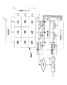
図1は、本発明の実施の形態1における撮像装置の概略構成を示す図である。
図1に示すように、実施の形態1の撮像装置は、撮像部1、負荷回路2、行選択エンコーダ3、列選択エンコーダ4、リード電圧出力部5、ノイズ除去部6、差分電圧出力部7、判断部8、及び、システム出力部9から構成される。
(Embodiment 1)
<Configuration>
FIG. 1 is a diagram showing a schematic configuration of an imaging apparatus according to
As illustrated in FIG. 1, the imaging apparatus according to the first embodiment includes an
撮像部1は、単位セルが1次元又は2次元上に配列された撮像領域である。ここでは、3×3の2次元上に配列された9画素の場合を例に取って説明するが、実際の画素数は、1次元で数千個、2次元で数十万〜数百万個程度である。
負荷回路2は、縦1列毎に同一の回路が1個接続されており、出力電圧を読み出す為に、列単位で撮像部1の画素に負荷をかける回路である。
The
The load circuit 2 is a circuit in which one identical circuit is connected for each vertical column, and a load is applied to the pixels of the
行選択エンコーダ3は、横1行毎に、“RESET”、“READ”、“LSEL”の3本の制御線を備え、撮像部1の画素に対して、行単位で、リセット(初期化)、リード(読み出し)、及び、ラインセレクト(行選択)を制御する。
列選択エンコーダ4は制御線を備え、列を順次選択して、リード電圧出力部5、ノイズ除去部6、及び、差分電圧出力部7を制御する。
The
The column selection encoder 4 includes a control line, and sequentially selects columns to control the read voltage output unit 5, the noise removal unit 6, and the differential voltage output unit 7.
リード電圧出力部5は、列選択エンコーダ4の制御により、撮像部1からの列単位のリード電圧を順次出力する。
ノイズ除去部6は、縦1列毎に同一の回路が1個接続されており、列選択エンコーダ4の制御により、リセット電圧とリード電圧との差分に相当する差分電圧を単位セル毎に生成する。
The read voltage output unit 5 sequentially outputs the read voltage in units of columns from the
The noise removal unit 6 is connected to one identical circuit for each vertical column, and generates a differential voltage corresponding to the difference between the reset voltage and the read voltage for each unit cell under the control of the column selection encoder 4. .
差分電圧出力部7は、列選択エンコーダ4の制御により、ノイズ除去部6により生成された差分電圧を順次出力する。
判断部8は、リード電圧出力部5により出力されたリード電圧が、それぞれ所定の範囲の電圧であるか否かを判断する。
システム出力部9は、差分電圧出力部7により出力された差分電圧のうちの、判断部8によりリード電圧が所定の範囲の電圧であると判断された単位セルに対応する差分電圧を、それぞれの単位セルに対応する輝度情報として後段の装置へ出力し、高輝度を示す所定の電圧を、判断部8によりリード電圧が所定の範囲の電圧であると判断されなかったそれぞれの単位セルに対応する輝度情報として後段の装置へ出力する。
The differential voltage output unit 7 sequentially outputs the differential voltage generated by the noise removing unit 6 under the control of the column selection encoder 4.
The
The
ここで、撮像部1、負荷回路2、行選択エンコーダ3、列選択エンコーダ4、リード電圧出力部5、ノイズ除去部6、及び、差分電圧出力部7は、半導体撮像素子の回路により実現され、判断部8、及び、システム出力部9は、汎用のコンピュータ及び専用のアプリケーションプログラムから構成される信号処理装置により実現される。
図2は、実施の形態1の半導体撮像素子の回路の概略を示す図である。
Here, the
FIG. 2 is a diagram showing an outline of a circuit of the semiconductor imaging device of the first embodiment.
図2に示すように、実施の形態1の半導体撮像素子の回路は、負荷回路100、画素回路110、信号処理回路120を備える。
負荷回路100は、図1の負荷回路2中の1個の回路を記載したものであり、第1信号出力線とGNDとの間に接続された負荷用トランジスタ101を含み、負荷電圧(LG)が供給される。
As shown in FIG. 2, the circuit of the semiconductor imaging device of the first embodiment includes a
The
画素回路110は、図1の撮像部1中の1個の単位セルを記載したものであり、初期化時の電圧を増幅したリセット電圧と読み出し時の電圧を増幅したリード電圧とを第1信号出力線に出力することを特徴とし、入射した光を光電変換し電荷を出力するフォトダイオード111と、電荷を蓄積し蓄積した電荷に応じた電圧を示すコンデンサ112と、コンデンサ112の示す電圧が初期電圧(ここではVDD)になるようにリセットするリセットトランジスタ113と、フォトダイオード111により出力される電荷をコンデンサ112に供給するリードトランジスタ114と、コンデンサ112の示す電圧に追従して変化する電圧を出力する増幅用トランジスタ115と、行選択エンコーダ3からラインセレクト信号を受けた時に増幅用トランジスタ115の出力を第1信号出力線に出力するラインセレクトトランジスタ116とを含む。
The
信号処理回路120は、図1のリード電圧出力部5路、ノイズ除去部6、及び、差分電圧出力部7中の縦1列用の1個の回路を記載したものであり、単位セルにより出力されるリセット電圧と当該リード電圧との差分を示す輝度情報を第2信号出力線に出力し、当該リセット電圧を第3信号出力線に出力することを特徴とし、第1信号出力線と第2信号出力線との間に直列に接続されたクランプ容量121及びサンプリングトランジスタ122と、クランプ容量121とサンプリングトランジスタ122とを接続する信号線と基準電圧端子VDDとの間に直列に接続されたクランプトランジスタ123と、第2信号出力線とGNDとの間に直列に接続されたサンプリング容量124と、第1信号出力線と第3信号出力線との間に直列に接続されたリード電圧選択トランジスタ125とを含む。
The
ここで、画素回路110には、リセットパルス(初期化信号:RESET)、リードパルス(読み出しパルス:READ)、及び、ラインセレクトパルス(行選択信号:LSEL)が、信号処理回路120には、サンプリングパルス(SP)、クランプパルス(CP)、及び、リード電圧選択パルス(RCSEL)が決められたタイミングで供給され、これら各制御パルスにそれぞれ対応するトランジスタが開閉(オフ/オン)される。
Here, the
図3は、実施の形態1の撮像装置における各制御パルスのタイミングの一例を示す図である。
図3に示すようなタイミングで各制御パルスを与えることで、ラインセレクトトランジスタ116を閉じたまま(オンにした状態で)、サンプリングトランジスタ122とクランプトランジスタ123とを閉じ(オンにし)第2信号出力線を基準電圧にした状態で第1信号出力線にリセット電圧を出力させ(図3のa)、基準電圧とリセット電圧との差分相当がクランプ容量121に保持され(図3のb)、その後、クランプトランジスタ123を開いて(オフして)リードトランジスタ114を閉じる(オンにする)ことにより第1信号出力線にリード電圧を出力させ(図3のc)、第2信号出力線の電圧が当該リセット電圧と当該リード電圧との差分相当だけ当該基準電圧から変化し(図3のd)、これを輝度情報として出力することができ、続いて、サンプリングトランジスタ122を開いた(オフした)後でリード電圧選択トランジスタ125を閉じ(オンにし)、第3信号出力線にリード電圧を出力させる(図3のe)。
FIG. 3 is a diagram illustrating an example of the timing of each control pulse in the imaging apparatus according to the first embodiment.
By giving each control pulse at the timing as shown in FIG. 3, the sampling transistor 122 and the clamp transistor 123 are closed (turned on) while the line select transistor 116 is closed (turned on), and the second signal output is performed. The reset voltage is output to the first signal output line with the line set to the reference voltage (a in FIG. 3), and the difference between the reference voltage and the reset voltage is held in the clamp capacitor 121 (b in FIG. 3). Then, by opening (turning off) the clamp transistor 123 and closing (turning on) the read transistor 114, the read voltage is output to the first signal output line (c in FIG. 3), and the voltage of the second signal output line is The difference from the reference voltage is equivalent to the difference between the reset voltage and the read voltage (d in FIG. 3), and this can be output as luminance information. Can, subsequently, opens the sampling transistor 122 (turned off) later close the read voltage selection transistor 125 (and on), and outputs the read voltage to the third signal output line (e in FIG. 3).
図4は、実施の形態1の撮像装置における各制御パルスのタイミングの他の例を示す図である。
図3の例では負荷用トランジスタ101を常時閉じたまま(オンにした状態)であるが、図4の例では負荷用トランジスタ101に負荷回路駆動パルスを与え、リード電圧をクランプ容量121に蓄積して、リード電圧を出力する前に負荷回路の駆動を止めることにより、低消費電力を実現するものである。
FIG. 4 is a diagram illustrating another example of the timing of each control pulse in the imaging apparatus according to the first embodiment.
In the example of FIG. 3, the load transistor 101 is always closed (turned on), but in the example of FIG. 4, a load circuit drive pulse is applied to the load transistor 101 and the read voltage is stored in the clamp capacitor 121. Thus, low power consumption is realized by stopping the drive of the load circuit before outputting the read voltage.
図4に示すようなタイミングで各制御パルスを与えることで、負荷用トランジスタ101を閉じ(オンにし)、ラインセレクトトランジスタ116を閉じたまま(オンにした状態で)、サンプリングトランジスタ122とクランプトランジスタ123とを閉じ(オンにし)第2信号出力線を基準電圧にした状態で第1信号出力線にリセット電圧を出力させ(図4のa)、基準電圧とリセット電圧との差分相当がクランプ容量121に保持され(図4のb)、その後、クランプトランジスタ123を開いて(オフして)リードトランジスタ114を閉じる(オンにする)ことにより第1信号出力線にリード電圧を出力させ(図4のc)、第2信号出力線の電圧が当該リセット電圧と当該リード電圧との差分相当だけ当該基準電圧から変化し(図4のd)、これを輝度情報として出力することができ、続いて、サンプリングトランジスタ122を開く(オフする)ことにより輝度情報が蓄積されたサンプリング容量124とクランプ容量121との接続を切り、負荷用トランジスタ101を開いた(オフした)後にラインセレクトトランジスタ116を開いて(オフして)、第1信号出力線をフローティングにしたまま、クランプトランジスタ123を閉じ(オンにし)クランプ容量121に基準電圧を印加した後、リード電圧選択トランジスタ125を閉じ(オンにし)、第3信号出力線にリード電圧を出力させる(図4のe)。 By giving each control pulse at the timing shown in FIG. 4, the load transistor 101 is closed (turned on), the line select transistor 116 is closed (turned on), and the sampling transistor 122 and the clamp transistor 123 are turned on. Are closed (turned on) and the second signal output line is set to the reference voltage, the reset voltage is output to the first signal output line (a in FIG. 4), and the difference between the reference voltage and the reset voltage corresponds to the clamp capacitor 121. (B in FIG. 4), and then the clamp transistor 123 is opened (turned off) and the read transistor 114 is closed (turned on), thereby causing the first signal output line to output a read voltage (shown in FIG. 4). c) The voltage of the second signal output line changes from the reference voltage by an amount corresponding to the difference between the reset voltage and the read voltage (see FIG. D), which can be output as luminance information, and then, by opening (turning off) the sampling transistor 122, the sampling capacitor 124 in which the luminance information is stored and the clamp capacitor 121 are disconnected, and the load After the transistor 101 is opened (turned off), the line select transistor 116 is opened (turned off), the clamp transistor 123 is closed (turned on) while the first signal output line is left floating, and the reference voltage is applied to the clamp capacitor 121. After the application, the read voltage selection transistor 125 is closed (turned on), and the read voltage is output to the third signal output line (e in FIG. 4).
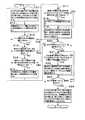
<動作>
図5は、判断部8、及び、システム出力部9における一画素あたりの信号処理の手順を示す図である。
以下に、図5を用いて一画素あたりの信号処理の手順を説明する。
(1)システム出力部9が、差分電圧出力部7から注目画素の差分電圧を受け取り、一時的に保持する(ステップS1)。
<Operation>
FIG. 5 is a diagram illustrating a signal processing procedure per pixel in the
Hereinafter, a signal processing procedure per pixel will be described with reference to FIG.
(1) The
(2)判断部8が、リード電圧出力部5から注目画素のリード電圧を受け取る(ステップS2)。
(3)判断部8が、受け取ったリード電圧が所定の範囲の電圧であるか否かを判断する(ステップS3)。
(4)判断部8により所定の範囲の電圧であると判断された場合には、システム出力部9が、一時的に保持しておいた差分電圧を、注目画素の輝度情報として出力する(ステップS4)。
(2) The
(3) The
(4) When the
(5)判断部8により所定の範囲の電圧であると判断されなかった場合には、システム出力部9が、高輝度を示す所定の電圧を注目画素の輝度情報として出力する(ステップS5)。
<まとめ>
図6(a)は、リセット時における第1信号出力線の電圧の特性を示す図である。
(5) If the
<Summary>
FIG. 6A is a diagram illustrating a voltage characteristic of the first signal output line at the time of reset.
図6(b)は、リード時における第1信号出力線の電圧の特性を示す図である。
図6(c)は、画像が暗くなったり画像が黒つぶれすることに対して何の対策も施していない従来の撮像装置における出力電圧の特性を示す図であり、−(図6(a)−図6(b))に相当する。
図6(d)は、本発明の実施の形態1の撮像装置における出力電圧の特性を示す図であり、所定の電圧を越えた場合には高輝度を示す電圧となるので画像が暗くなったり画像が黒つぶれすることが一切ない。
FIG. 6B is a diagram illustrating a voltage characteristic of the first signal output line at the time of reading.
FIG. 6C is a diagram illustrating output voltage characteristics in a conventional imaging device that does not take any measures against dark images or blackened images, and FIG. -Corresponds to FIG.
FIG. 6D is a diagram showing the characteristics of the output voltage in the imaging apparatus according to
ここで図6(a)〜(d)において、横軸は入射光の強さ(右が強い)、縦軸は電圧((a),(b)は上がプラス、(c),(d)は上がマイナス)を示す。
以上のように、本発明の実施の形態1では、図6(b)に示したリード時の電圧に着目し、リード時の電圧が増幅回路が飽和する辺りの電圧に達した事を判断し、黒つぶれが発生している可能性がある出力電圧を高輝度を示す電圧に置き換えるので、画像が暗くなったり黒つぶれが発生する入射光よりも充分弱い入射光から余裕をもって対策することにより、強い光を入射したときに画像が黒つぶれするという問題点を従来よりも確実に解決し、またリセット時の電圧の変化による悪影響を確実に排除することができる。
(実施の形態2)
<構成>
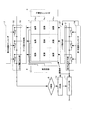
図7は、本発明の実施の形態2における撮像装置の概略構成を示す図である。
6A to 6D, the horizontal axis indicates the intensity of incident light (right is strong), the vertical axis indicates voltage ((a) and (b) are positive, and (c) and (d). ) Indicates minus on the top.
As described above, in
(Embodiment 2)
<Configuration>
FIG. 7 is a diagram illustrating a schematic configuration of the imaging apparatus according to Embodiment 2 of the present invention.
図7に示すように、実施の形態2の撮像装置は、撮像部1、負荷回路2、行選択エンコーダ3、列選択エンコーダ4、リード電圧出力部5、ノイズ除去部6、差分電圧出力部7、判断部8、選択部10、及び、システム出力部11から構成される。
なお、実施の形態1と同様の構成要素には同一番号を付し、その説明を省略する。
選択部10は、差分電圧出力部7により出力された差分電圧に基づいて、判断部8によりリード電圧が所定の範囲の電圧であると判断されなかったリード電圧に対応する単位セルの中から、補正対象の単位セルを選択する。
As illustrated in FIG. 7, the imaging apparatus according to the second embodiment includes an
In addition, the same number is attached | subjected to the component similar to
Based on the differential voltage output from the differential voltage output unit 7, the
図8は、選択部10の詳細な構成を示す図である。
図8に示すように、選択部10は、単位セル抽出部12、領域区分部13、領域抽出部14、及び、単位セル選択部15を含む。
単位セル抽出部12は、判断部8により所定の範囲の電圧であると判断されなかったリード電圧に対応する単位セルのうちの、対応する差分電圧が飽和電圧でない単位セルを抽出する。
FIG. 8 is a diagram illustrating a detailed configuration of the
As illustrated in FIG. 8, the
The unit
領域区分部13は、単位セル抽出部12により抽出された単位セルを、配列上において連続する領域毎に区分する。
領域抽出部14は、領域区分部13により区分された領域のうち、各領域に隣接する単位セルに対応する差分電圧の全部又は一部が飽和電圧である領域を抽出する。
単位セル選択部15は、領域抽出部14により抽出された領域内の単位セルを、補正対象の単位セルとして選択する。
The
The
The unit
システム出力部11は、差分電圧出力部7により出力された差分電圧のうちの
、単位セル選択部15により補正対象として選択されなかった補正対象以外の単位セルに対応する差分電圧を、それぞれの単位セルに対応する輝度情報として後段の装置へ出力し、高輝度を示す所定の電圧を、単位セル選択部15により補正対象として選択されたそれぞれの単位セルに対応する輝度情報として後段の装置へ出力する。
The system output unit 11 outputs the differential voltages corresponding to the unit cells other than the correction target that are not selected as the correction target by the unit
ここで、撮像部1、負荷回路2、行選択エンコーダ3、列選択エンコーダ4、リード電圧出力部5、ノイズ除去部6、及び、差分電圧出力部7は、半導体素子の回路により実現され、判断部8、選択部10、及び、システム出力部11は、汎用のコンピュータ及び専用のアプリケーションプログラムから構成される信号処理装置により実現される。
<動作>
図9は、判断部8、選択部10、及び、システム出力部11における信号処理の手順を示す図である。
Here, the
<Operation>
FIG. 9 is a diagram illustrating a signal processing procedure in the
以下に、図9を用いて信号処理の手順を説明する。
(1)システム出力部11が、差分電圧出力部7から注目単位セルの差分電圧を受け取り、注目単位セルの配列上の位置情報と対応付けて保持する(ステップS11)。
(2)判断部8が、リード電圧出力部5から注目画素のリード電圧を受け取る(ステップS12)。
Hereinafter, a signal processing procedure will be described with reference to FIG.
(1) The system output unit 11 receives the differential voltage of the target unit cell from the differential voltage output unit 7, and stores it in association with the positional information on the array of the target unit cell (step S11).
(2) The
(3)判断部8が、受け取ったリード電圧が所定の範囲の電圧であるか否かを判断する(ステップS13)。所定の範囲の電圧であると判断された場合は注目単位セルの配列上の位置情報には領域番号を付加しない。
(4)判断部8により所定の範囲の電圧であると判断されなかった場合には、単位セル抽出部12が、対応する差分電圧が飽和電圧であるか否かを判断する(ステップS14)。
(3) The
(4) If the
(5)対応する差分電圧が飽和電圧であると判断されなかった場合には、領域区分部13が、注目単位セルの配列上の位置情報と、既に記録されている他の単位セルの配列上の位置情報とを比較して、配列上において隣接する関係にある他の単位セルが記録されているか否かを判断する(ステップS15)。
(6)隣接する関係にある他の単位セルが記録されていない場合には、注目単位セルの配列上の位置情報に新しい領域番号を付けて記憶する(ステップS16)。
(5) If it is not determined that the corresponding differential voltage is a saturation voltage, the
(6) If no other unit cell having an adjacent relationship is recorded, the position information on the array of the unit cell of interest is added with a new area number and stored (step S16).
(7)隣接する関係にある他の単位セルが記録されている場合には、隣接する関係にある他の単位セルに付けられている領域番号が全て同じであるか否かを判断する(ステップS17)。
(8)領域番号が全て同じでない場合には、全て同じ1つの領域番号を付け直す(ステップS18)。
(7) When other unit cells having an adjacent relationship are recorded, it is determined whether or not the area numbers assigned to the other unit cells having the adjacent relationship are all the same (step) S17).
(8) If all the area numbers are not the same, all the same area numbers are reassigned (step S18).
(9)注目単位セルの配列上の位置情報に、隣接する関係にある他の単位セルに付けられている領域番号を付けて記憶する(ステップS19)。
(10)全ての単位セルについて、上記の処理を繰り返す(ステップS20)。
(11)領域抽出部14が、注目領域に隣接する単位セルの全部又は一部に対応する差分電圧が飽和電圧であるか否かを判断する(ステップS21)。
(9) The position information on the arrangement of the unit cell of interest is stored with the region number assigned to the other unit cells in the adjacent relationship (step S19).
(10) The above process is repeated for all unit cells (step S20).
(11) The
ここで、注目領域に隣接する単位セルの一部のみを判断対象とする場合の判断対象の単位セルの決め方は、例えば、単位セルの配列を(X,Y)で記述すると、注目領域内の全ての単位セルのXの中心値又は平均値を判断対象の単位セルのX値とし、当該X値を持つ注目領域内の単位セルのうちの、Y値の最大値+1又はY値の最小値−1とをY値とする。 Here, when only a part of the unit cells adjacent to the attention area is to be determined, the determination method of the unit cell to be determined is, for example, by describing the arrangement of unit cells as (X, Y). The center value or average value of X of all unit cells is set as the X value of the unit cell to be determined, and among the unit cells in the attention area having the X value, the maximum Y value + 1 or the minimum Y value Let -1 be the Y value.
(12)飽和電圧であると判断された場合には、単位セル選択部15が、注目領域内の単位セルを補正対象の単位セルとして選択して、それらの位置情報を記録する(ステップS22)。
(13)全ての領域について、上記の処理を繰り返す(ステップS23)。
(14)システム出力部11が、差分電圧出力部7により出力された差分電圧のうちの単位セル選択部15により補正対象として選択されなかった補正対象以外の単位セルに対応する差分電圧を、それぞれの単位セルに対応する輝度情報として後段の装置へ出力し、高輝度を示す所定の電圧を、単位セル選択部15により補正対象として選択されたそれぞれの単位セルに対応する輝度情報として後段の装置へ出力する(ステップS24)。
(12) If it is determined that the voltage is the saturation voltage, the unit
(13) The above processing is repeated for all regions (step S23).
(14) The system output unit 11 outputs differential voltages corresponding to unit cells other than the correction target that are not selected as the correction target by the unit
<まとめ>
以上のように、本発明の実施の形態2では、実施の形態1と同様に図6(b)に示したリード時の電圧に着目し、リード時の電圧が増幅回路が飽和する辺りの電圧に達した事を判断し、さらに、差分電圧を考慮して黒つぶれが発生しているであろうと推測される領域における出力電圧を高輝度を示す電圧に置き換えるので、画像が暗くなったり黒つぶれが発生する入射光よりも充分弱い入射光から余裕をもって対策することにより、強い光を入射したときに画像が黒つぶれするという問題点を従来よりも確実に解決し、またリセット時の電圧の変化による悪影響を確実に排除することができる。
(変形例1)
通常、CMOSセンサ等の半導体撮像素子は、撮像部に対して一方にノイズ除去部があるために光学中心とチップセンタとがずれている。
<Summary>
As described above, in the second embodiment of the present invention, attention is paid to the voltage at the time of reading shown in FIG. 6B as in the case of the first embodiment. In addition, the output voltage in the area where blackout is supposed to have occurred considering the differential voltage is replaced with a voltage indicating high brightness, so the image becomes darker or blackout occurs. By taking sufficient measures from incident light that is sufficiently weaker than incident light that generates light, the problem that the image will be blacked out when strong light is incident is solved more reliably than before, and the voltage change at reset The adverse effects due to can be reliably eliminated.
(Modification 1)
Usually, a semiconductor image pickup device such as a CMOS sensor has a noise removal portion on one side with respect to the image pickup portion, so that the optical center and the chip center are shifted.
本願の半導体撮像素子は、従来の半導体撮像素子と比較して、リード電圧を出力するために、トランジスタ等のスイッチング素子、及びコンデンサ等の容量素子や、増幅回路等が増える。
そこで、変形例1は、リード電圧を出力するため増加部分を、撮像部を中心に差分電圧出力部とは対称的な位置に配置することにより、光学中心とチップセンタとのずれを少なくするものである。
Since the semiconductor image pickup device of the present application outputs a read voltage as compared with a conventional semiconductor image pickup device, a switching element such as a transistor, a capacitance element such as a capacitor, an amplifier circuit, and the like increase.
Therefore, in the first modification, the increase portion for outputting the read voltage is arranged at a position symmetrical to the differential voltage output portion with the imaging portion as the center, thereby reducing the deviation between the optical center and the chip center. It is.
<構成>
図10は、本発明の変形例1における撮像装置の概略構成を示す図である。
図10に示すように、変形例1の撮像装置は、撮像部1、負荷回路2、行選択エンコーダ3、第1列選択エンコーダ16、第2列選択エンコーダ17、リード電圧保持部18、リード電圧出力部19、ノイズ除去部20、差分電圧出力部21、判断部8、及び、システム出力部9から構成される。
<Configuration>
FIG. 10 is a diagram showing a schematic configuration of an imaging apparatus according to
As shown in FIG. 10, the imaging apparatus of
なお、実施の形態1と同様の構成要素には同一番号を付し、その説明を省略する。
第1列選択エンコーダ16は制御線を備え、列を順次選択してリード電圧保持部18、及び、リード電圧出力部19を制御するものであり、第2列選択エンコーダ17と撮像部1を中心に対称的な位置に配置されている。
第2列選択エンコーダ17は制御線を備え、列を順次選択してノイズ除去部20、及び、差分電圧出力部21を制御するものであり、第1列選択エンコーダ16と撮像部1を中心に対称的な位置に配置されている。
In addition, the same number is attached | subjected to the component similar to
The first
The second
リード電圧保持部18は、第1列選択エンコーダ16の制御により、撮像部1からのリード電圧を順次蓄積して、そのまま、又は増幅して出力するものであり、ノイズ除去部20と撮像部1を中心に対称的な位置に配置されている。
リード電圧出力部19は、第1列選択エンコーダ16の制御により、リード電圧保持部18によ保持されたリード電圧を順次出力するものであり、差分電圧出力部21と撮像部1を中心に対称的な位置に配置されている。
The read
The read
ノイズ除去部20は、縦1列毎に同一の回路が1個接続されており、第2列選択エンコーダ17の制御により、リセット電圧とリード電圧との差分に相当する差分電圧を単位セル毎に生成するものであり、リード電圧保持部18と撮像部1を中心に対称的な位置に配置されている。
差分電圧出力部21は、第2列選択エンコーダ17の制御により、ノイズ除去部20により生成された差分電圧を順次出力するものであり、リード電圧出力部19と撮像部1を中心に対称的な位置に配置している。
The
The differential
ここで図10は実施の形態1に対する変形例であるので、実施の形態2に対する同様な変形例を以下に示す。
図11は、本発明の変形例1における撮像装置の概略構成を示す図である。
図11に示すように、変形例1の撮像装置は、撮像部1、負荷回路2、行選択エンコーダ3、第1列選択エンコーダ16、第2列選択エンコーダ17、リード電圧保持部18、リード電圧出力部19、ノイズ除去部20、差分電圧出力部21、判断部8、選択部10、及び、システム出力部11から構成される。
Here, since FIG. 10 is a modification to the first embodiment, a similar modification to the second embodiment is shown below.
FIG. 11 is a diagram illustrating a schematic configuration of an imaging apparatus according to
As shown in FIG. 11, the imaging device of
なお、実施の形態2と同様の構成要素には同一番号を付し、その説明を省略する。
<まとめ>
以上のように、本発明の変形例1では、リード電圧を出力するため増加部分を、撮像部を中心に差分電圧出力部とは対称的な位置に配置するので、光学中心とチップセンタとのずれを少なくすることができる。
(変形例2)
<構成>
図12は、変形例2の半導体素子の回路の概略を示す図である。
In addition, the same number is attached | subjected to the component similar to Embodiment 2, and the description is abbreviate | omitted.
<Summary>
As described above, in
(Modification 2)
<Configuration>
FIG. 12 is a diagram showing an outline of a circuit of the semiconductor element of the second modification.
図12に示すように、変形例2の半導体素子の回路は、負荷回路100、画素回路110、信号処理回路130を備える。
なお、実施の形態1と同様の構成要素には同一番号を付し、その説明を省略する。
信号処理回路130は、図1のリード電圧出力部5、ノイズ除去部6、及び、差分電圧出力部7中の縦1列用の1個の回路を記載したものであり、単位セルにより出力されるリセット電圧と当該リード電圧との差分を示す輝度情報を第4信号出力線に出力し、当該リセット電圧を第3信号出力線に出力することを特徴とし、第1信号出力線と第2信号出力線との間に直列に接続されたサンプリングトランジスタ131、及び、クランプ容量132と、第2信号出力線とGNDとの間に直列に接続されたサンプリング容量133と、第2信号出力線と基準電圧端子VDDとの間に直列に接続されたクランプトランジスタ134と、第2信号出力線と第4信号出力線との間に直列に接続された差分電圧選択トランジスタ135と、サンプリングトランジスタ131とクランプ容量132とを接続する信号線を入力とする増幅回路136と、増幅回路136の出力と第3信号出力線との間に直列に接続されたリード信号選択トランジスタ137とを含む。
As illustrated in FIG. 12, the circuit of the semiconductor element according to Modification 2 includes a
In addition, the same number is attached | subjected to the component similar to
The
ここで、画素回路110には、リセットパルス(初期化信号:RESET)、リードパルス(読み出しパルス:READ)、及び、ラインセレクトパルス(行選択信号:LSEL)が、信号処理回路130には、サンプリングパルス(SP)、クランプパルス(CP)、差分電圧選択パルス(SCSEL)、及び、リード電圧選択パルス(RCSEL)が決められたタイミングで供給され、これら各制御パルスにそれぞれ対応するトランジスタが開閉(オフ/オン)される。
Here, the
図13は、変形例2の撮像装置における各制御パルスのタイミングの一例を示す図である。
図13に示すようなタイミングで各制御パルスを与えることで、負荷用トランジスタ101を閉じ(オンにし)、ラインセレクトトランジスタ116を閉じたまま(オンにした状態で)、サンプリングトランジスタ131とクランプトランジスタ134とを閉じ(オンにし)第2信号出力線を基準電圧にした状態で第1信号出力線にリセット電圧を出力させ(図13のa)、基準電圧とリセット電圧との差分相当がクランプ容量132に保持され(図13のb)、その後、クランプトランジスタ134を開いて(オフして)リードトランジスタ114を閉じる(オンにする)ことにより第1信号出力線にリード電圧を出力させ(図13のc)、第2信号出力線の電圧が当該リセット電圧と当該リード電圧との差分相当だけ当該基準電圧から変化し(図13のd)、続いて、サンプリングトランジスタ131を開く(オフする)ことにより第1信号出力線とクランプ容量132との接続を切り、その後低消費電力のため負荷用トランジスタ101とラインセレクトトランジスタ116とを開き(オフし)、リード信号選択トランジスタ137を開く(オフする)ことにより第3信号出力線にリード電圧を出力させ(図13のe)、差分電圧選択トランジスタ135を開く(オフする)ことにより第4信号出力線に差分電圧を出力させる(図13のf)。
FIG. 13 is a diagram illustrating an example of the timing of each control pulse in the imaging apparatus according to the second modification.
By giving each control pulse at a timing as shown in FIG. 13, the load transistor 101 is closed (turned on), the line select transistor 116 is kept closed (turned on), and the sampling transistor 131 and the clamp transistor 134 Are closed (turned on) and the second signal output line is set to the reference voltage, and the reset voltage is output to the first signal output line (a in FIG. 13), and the difference between the reference voltage and the reset voltage corresponds to the clamp capacitor 132. (B in FIG. 13), and then the clamp transistor 134 is opened (turned off) and the read transistor 114 is closed (turned on) to output the read voltage to the first signal output line (FIG. 13). c) The voltage of the second signal output line is changed from the reference voltage by an amount corresponding to the difference between the reset voltage and the read voltage. (D in FIG. 13), then, the sampling transistor 131 is opened (turned off) to disconnect the first signal output line from the clamp capacitor 132, and then the load transistor 101 and the line select for low power consumption. The transistor 116 is opened (turned off), and the read signal selection transistor 137 is opened (turned off) to output a read voltage to the third signal output line (e in FIG. 13), and the differential voltage selection transistor 135 is opened (off). To output a differential voltage to the fourth signal output line (f in FIG. 13).
なお、増幅回路136があるために、第3信号出力線に出力したリード電圧は、読み出される際に破壊しないので、リード電圧を読み出しても差分電圧は変化せず、リード電圧を差分電圧よりも先に読み出すことができる。
<まとめ>
以上のように、本発明の変形例2では、リード電圧を差分電圧よりも先に読み出すことができる。
Since the read voltage output to the third signal output line is not destroyed when it is read because of the amplifier circuit 136, the differential voltage does not change even when the read voltage is read, and the read voltage is set higher than the differential voltage. It can be read out first.
<Summary>
As described above, in the second modification of the present invention, the read voltage can be read before the differential voltage.
本発明の各実施例においては、リード電圧に基づく判断及び処理を先に行う必要があるため、リード電圧を差分電圧よりも先に読み出すことにより、判断及び処理時間を短縮できる。
(変形例3)
<構成>
図14は、画素回路の変形例を示す図である。
In each embodiment of the present invention, since it is necessary to perform the determination and processing based on the read voltage first, the determination and processing time can be shortened by reading the read voltage before the differential voltage.
(Modification 3)
<Configuration>
FIG. 14 is a diagram illustrating a modification of the pixel circuit.
本発明の変形例3では、本発明の実施の形態1における図2に示す画素回路110を、図14に示す画素回路140に置き換える。
図14に示す画素回路140は、初期化時の電圧を増幅したリセット電圧と読み出し時の電圧を増幅したリード電圧とを第1信号出力線に出力することを特徴とし、入射した光を光電変換し電荷を発生させて蓄積し、蓄積された電荷を電圧信号として出力するフォトダイオード等の受光素子141と、受光素子141に蓄積された電荷を掃き出して受光素子141の電圧が初期電圧(ここではVDD)になるようにリセットするリセットトランジスタ142と、受光素子141に蓄積された電荷により発生する電圧に追従して変化する電圧を出力する増幅トランジスタ143と、行選択エンコーダ3からラインセレクト信号を受けた時に増幅トランジスタ143の出力を第1信号出力線に出力するラインセレクトトランジスタ144とを含む。
In
The
図15は、変形例3の撮像装置における各制御パルスのタイミングの一例を示す図である。
図15に示すようなタイミングで各制御パルスを与えることで、ラインセレクトトランジスタ144を閉じたまま(オンにした状態で)、第1信号出力線に受光素子141に蓄積された電荷に応じたリード電圧を出力させ(図15のa〜b)、その後、リセットパルスを与えて(図15のc)、第1信号出力線にリセット電圧を出力させる(図15のd)。
FIG. 15 is a diagram illustrating an example of the timing of each control pulse in the imaging apparatus according to the third modification.
By giving each control pulse at a timing as shown in FIG. 15, the line select transistor 144 is closed (in an on state), and the read corresponding to the electric charge accumulated in the light receiving element 141 in the first signal output line is performed. A voltage is output (ab in FIG. 15), and then a reset pulse is applied (c in FIG. 15) to output a reset voltage to the first signal output line (d in FIG. 15).
<まとめ>
以上のように、本発明の変形例3では、リードトランジスタを含まない画素回路を用いることができる。
なお、本発明の各実施例の形態および各変形例においては、MOS型増幅トランジスタを例にとり説明したが、CMD、BASIS、SIT等の固定パターンノイズ除去回路を必要とするあらゆる撮像装置に適用することができる。
<Summary>
As described above, in the third modification of the present invention, a pixel circuit that does not include a read transistor can be used.
In the embodiments and modifications of the embodiments of the present invention, the description has been given by taking the MOS amplification transistor as an example. However, the present invention is applicable to any imaging device that requires a fixed pattern noise removal circuit such as CMD, BASIS, or SIT. be able to.
本発明は、家庭用ビデオカメラやデジタルスチルカメラなどの撮像機器に適用することができる。本発明によって、単位画素の表面積を縮小しても信号電荷の残留が生じにくい固体撮像素子が提供でき、撮像機器の画質の向上やコストダウンに寄与することができる。
また、家庭用だけでなく、あらゆる撮像機器に適用することができる。
The present invention can be applied to imaging devices such as home video cameras and digital still cameras. According to the present invention, it is possible to provide a solid-state imaging device in which signal charges are unlikely to remain even when the surface area of a unit pixel is reduced, which can contribute to improvement in image quality and cost reduction of imaging equipment.
Further, it can be applied not only to home use but also to any imaging device.
図6(b)は、リード時における第1信号出力線の電圧の特性を示す図である。
図6(c)は、画像が暗くなったり画像が黒つぶれすることに対して何の対策も施していない従来の撮像装置における出力電圧の特性を示す図である。
図6(d)は、本発明の実施の形態1の撮像装置における出力電圧の特性を示す図である。
FIG. 6C is a diagram illustrating output voltage characteristics in a conventional imaging device that does not take any measures against dark images or blackened images.
FIG. 6D is a diagram illustrating output voltage characteristics in the imaging apparatus according to
1 撮像部
2 負荷回路
3 行選択エンコーダ
4 列選択エンコーダ
5 リード電圧出力部
6 ノイズ除去部
7 差分電圧出力部
8 判断部
9 システム出力部
10 選択部
11 システム出力部
12 単位セル抽出部
13 領域区分部
14 領域抽出部
15 単位セル選択部
16 第1列選択エンコーダ
17 第2列選択エンコーダ
18 リード電圧保持部
19 リード電圧出力部
20 ノイズ除去部
21 差分電圧出力部
100 負荷回路
101 負荷用トランジスタ
110 画素回路
111 フォトダイオード
112 コンデンサ
113 リセットトランジスタ
114 リードトランジスタ
115 増幅用トランジスタ
116 ラインセレクトトランジスタ
120 信号処理回路
121 クランプ容量
122 サンプリングトランジスタ
123 クランプトランジスタ
124 サンプリング容量
125 リード電圧選択トランジスタ
130 信号処理回路
131 サンプリングトランジスタ
132 クランプ容量
133 サンプリング容量
134 クランプトランジスタ
135 差分電圧選択トランジスタ
136 増幅回路
137 リード信号選択トランジスタ
140 画素回路
141 受光素子
142 リセットトランジスタ
143 増幅用トランジスタ
144 ラインセレクトトランジスタ
DESCRIPTION OF
Claims (17)
撮像素子は、
1画素に相当する光電変換部と、初期化時の当該光電変換部の出力電圧に対応するリセット電圧、及び受光量に応じた当該光電変換部の出力電圧に対応するリード電圧を生成し出力する出力部とを含む単位セルが、1次元、又は2次元状に複数個配列された撮像手段と、
前記リセット電圧と前記リード電圧との差分に相当する差分電圧を、前記単位セル毎に生成する差分電圧生成手段と、
前記リード電圧と前記差分電圧とを、信号処理装置へ単位セル毎に出力する素子出力手段とを備え、
信号処理装置は、
前記素子出力手段により単位セル毎に出力されたリード電圧が、それぞれ所定の範囲の電圧であるか否かに基づいて、補正対象の単位セルを選定する選定手段と、
前記素子出力手段により単位セル毎に出力された差分電圧のうちの、前記補正対象の単位セル以外の単位セルに対応する差分電圧を、それぞれの単位セルに対応する輝度情報として後段の装置へ出力し、高輝度を示す所定の電圧を、前記補正対象の単位セルに対応するそれぞれの輝度情報として後段の装置へ出力するシステム出力手段とを備えること
を特徴とする撮像システム。 An imaging system that includes an imaging element and a signal processing device and outputs luminance information corresponding to the amount of received light to a subsequent device,
The image sensor
A photoelectric conversion unit corresponding to one pixel, a reset voltage corresponding to the output voltage of the photoelectric conversion unit at initialization, and a read voltage corresponding to the output voltage of the photoelectric conversion unit corresponding to the amount of received light are generated and output. An imaging means in which a plurality of unit cells including an output unit are arranged in a one-dimensional or two-dimensional manner;
Differential voltage generation means for generating a differential voltage corresponding to the difference between the reset voltage and the read voltage for each unit cell;
Device output means for outputting the read voltage and the differential voltage to the signal processing device for each unit cell;
The signal processing device
Selection means for selecting a unit cell to be corrected based on whether or not the read voltage output for each unit cell by the element output means is a voltage within a predetermined range;
Of the differential voltage output for each unit cell by the element output means, the differential voltage corresponding to the unit cell other than the unit cell to be corrected is output to the subsequent apparatus as luminance information corresponding to each unit cell. And a system output unit that outputs a predetermined voltage indicating high luminance to each subsequent apparatus as luminance information corresponding to the unit cell to be corrected.
前記素子出力手段により単位セル毎に出力されたリード電圧が、それぞれ所定の範囲の電圧であるか否かを判断する判断手段と、
前記素子出力手段により単位セル毎に出力された差分電圧に基づいて、前記判断手段によりリード電圧が所定の範囲の電圧であると判断されなかったリード電圧に対応する単位セルの中から、補正対象の単位セルを選択する選択手段とを含むこと
を特徴とする請求項1に記載の撮像システム。 The selecting means is
Determining means for determining whether or not the read voltage output for each unit cell by the element output means is a voltage within a predetermined range;
Based on the differential voltage output for each unit cell by the element output unit, a correction target is selected from among the unit cells corresponding to the read voltage whose read voltage is not determined to be in a predetermined range by the determination unit. The imaging system according to claim 1, further comprising selection means for selecting a unit cell.
前記判断手段によりリード電圧が所定の範囲の電圧であると判断されなかったリード電圧に対応する単位セルのうちの、対応する差分電圧が飽和電圧でない単位セルが、配列上において連続する領域であって、かつ、当該領域に隣接する単位セルに対応する差分電圧が飽和電圧である領域を抽出し、当該領域内の単位セルを、補正対象の単位セルとして選択すること
を特徴とする請求項2に記載の撮像システム。 The selection means includes
Of the unit cells corresponding to the read voltage whose read voltage is not determined to be in a predetermined range by the determining means, unit cells whose corresponding differential voltage is not the saturation voltage are continuous regions on the array. And extracting a region in which a differential voltage corresponding to a unit cell adjacent to the region is a saturation voltage, and selecting a unit cell in the region as a unit cell to be corrected. The imaging system described in 1.
前記単位セルのそれぞれにより生成されたリード電圧を、前記信号処理装置へ出力するリード電圧出力手段と、
前記差分電圧生成手段により生成された差分電圧を、前記信号処理装置へ出力する差分電圧出力手段とを含み、
リード電圧出力手段と差分電圧出力手段とは、前記撮像手段を中心に、対称的な位置に配置されていること
を特徴とする請求項1に記載の撮像システム。 The element output means includes
Read voltage output means for outputting the read voltage generated by each of the unit cells to the signal processing device;
Differential voltage output means for outputting the differential voltage generated by the differential voltage generation means to the signal processing device,
The imaging system according to claim 1, wherein the read voltage output unit and the differential voltage output unit are arranged at symmetrical positions with the imaging unit as a center.
前記単位セルから、前記リセット電圧及び前記リード電圧が出力される第1出力線と、
後段の回路へ前記輝度情報を出力する第2出力線と、
前記第1出力線と前記第2出力線との間に、直列に接続されたクランプ容量と、
前記第2出力線と所定の電圧端子との間に直列に接続されたサンプリング容量と、
前記第2出力線と基準電圧端子との間に直列に接続されたクランプトランジスタとを含み、
前記撮像手段は、クランプ容量に保持された電圧をリード電圧として、前記第1出力線を介して前記素子出力手段に伝送し、
前記差分電圧生成手段は、サンプリング容量に保持された電圧を差分電圧として、前記第2出力線を介して前記素子出力手段に伝送すること
を特徴とする請求項1に記載の撮像システム。 The differential voltage generating means
A first output line from which the reset voltage and the read voltage are output from the unit cell;
A second output line for outputting the luminance information to a subsequent circuit;
A clamp capacitor connected in series between the first output line and the second output line;
A sampling capacitor connected in series between the second output line and a predetermined voltage terminal;
A clamp transistor connected in series between the second output line and a reference voltage terminal;
The imaging means transmits the voltage held in the clamp capacitor as a lead voltage to the element output means via the first output line,
The imaging system according to claim 1, wherein the differential voltage generation unit transmits the voltage held in the sampling capacitor as the differential voltage to the element output unit via the second output line.
前記単位セル毎に前記第1出力線との間に直列に接続され、単位セルの選択に用いられるセレクトトランジスタと、
前記第1出力線に負荷をかけることができ、前記出力電圧の読み出しに用いられる負荷回路と、
前記第1出力線と負荷回路との間に直列に接続される負荷用トランジスタとを含み、
撮像装置は、さらに、
セレクトトランジスタをオフすることにより単位セルを非導通とする前に、負荷用トランジスタをオフして負荷回路を遮断することによって、リード電圧を第1出力線に保持する制御手段を備えること
を特徴とする請求項5に記載の撮像装置。 The imaging means includes
A select transistor connected in series between each unit cell and the first output line and used for selecting a unit cell;
A load circuit capable of applying a load to the first output line and used for reading the output voltage;
A load transistor connected in series between the first output line and a load circuit;
The imaging device further includes
A control means for holding the read voltage on the first output line by turning off the load transistor and shutting off the load circuit before the unit cell is turned off by turning off the select transistor. The imaging device according to claim 5.
前記第1出力線と前記クランプ容量との間に配置されたサンプリングトランジスタを含み、
前記素子出力手段は、
入力端子がサンプリングトランジスタとクランプ容量の間に接続されており、前記単位セルのそれぞれにより生成され、クランプ容量に保持されたリード電圧を増幅して、前記信号処理装置へ出力するリード電圧出力手段を含むこと
を特徴とする請求項5に記載の撮像装置。 The differential voltage generation means further includes
A sampling transistor disposed between the first output line and the clamp capacitor;
The element output means includes
An input terminal is connected between the sampling transistor and the clamp capacitor, and a read voltage output means for amplifying the read voltage generated by each of the unit cells and held in the clamp capacitor and outputting the amplified read voltage to the signal processing device. The imaging device according to claim 5, comprising:
1画素に相当する光電変換部と、初期化時の当該光電変換部の出力電圧に対応するリセット電圧、及び受光量に応じた当該光電変換部の出力電圧に対応するリード電圧を生成し出力する出力部とを含む単位セルが、1次元、又は2次元状に複数個配列された撮像手段と、
前記リセット電圧と前記リード電圧との差分に相当する差分電圧を、前記単位セル毎に生成する差分電圧生成手段と、
前記リード電圧と前記差分電圧とを前記単位セル毎に出力する出力手段と
を備えることを特徴とする撮像素子。 An imaging device,
A photoelectric conversion unit corresponding to one pixel, a reset voltage corresponding to the output voltage of the photoelectric conversion unit at initialization, and a read voltage corresponding to the output voltage of the photoelectric conversion unit corresponding to the amount of received light are generated and output. An imaging means in which a plurality of unit cells including an output unit are arranged in a one-dimensional or two-dimensional manner;
Differential voltage generation means for generating a differential voltage corresponding to the difference between the reset voltage and the read voltage for each unit cell;
An image pickup device comprising: output means for outputting the read voltage and the differential voltage for each unit cell.
前記撮像素子から単位セル毎に出力されたリード電圧が、それぞれ所定の範囲の電圧であるか否かに基づいて、補正対象の単位セルを選定する選定手段と、
前記撮像素子からり単位セル毎に出力された差分電圧のうちの、前記補正対象の単位セル以外の単位セルに対応する差分電圧を、それぞれの単位セルに対応する輝度情報として後段の装置へ出力し、高輝度を示す所定の電圧を、前記補正対象の単位セルに対応するそれぞれの輝度情報として後段の装置へ出力する出力手段と
を備えることを特徴とする信号処理装置。 Each unit cell corresponding to the difference between the reset voltage for each unit cell corresponding to the output voltage of the photoelectric conversion unit at the time of initialization and the read voltage corresponding to the output voltage of the photoelectric conversion unit corresponding to the received light amount Is a signal processing device that receives and processes the differential voltage from the image sensor,
Selection means for selecting a unit cell to be corrected based on whether or not the read voltage output from the image sensor for each unit cell is a voltage in a predetermined range;
Of the differential voltage output for each unit cell from the image sensor, the differential voltage corresponding to the unit cell other than the unit cell to be corrected is output to the subsequent apparatus as luminance information corresponding to each unit cell. And an output means for outputting a predetermined voltage indicating high luminance to each subsequent apparatus as luminance information corresponding to the unit cell to be corrected.
前記撮像素子から単位セル毎に出力されたリード電圧が、それぞれ所定の範囲の電圧であるか否かを判断する判断手段と、
前記撮像素子から単位セル毎に出力された差分電圧に基づいて、前記判断手段によりリード電圧が所定の範囲の電圧であると判断されなかったリード電圧に対応する単位セルの中から、補正対象の単位セルを選択する選択手段とを含むこと
を特徴とする請求項9に記載の信号処理装置。 The selecting means is
Determination means for determining whether or not the read voltage output for each unit cell from the image sensor is a voltage within a predetermined range;
Based on the differential voltage output for each unit cell from the image sensor, the determination unit selects a correction target from the unit cells corresponding to the read voltage whose read voltage is not determined to be within a predetermined range. The signal processing apparatus according to claim 9, further comprising selection means for selecting a unit cell.
前記判断手段によりリード電圧が所定の範囲の電圧であると判断されなかったリード電圧に対応する単位セルのうちの、対応する差分電圧が飽和電圧でない単位セルが、配列上において連続する領域であって、かつ、当該領域に隣接する単位セルに対応する差分電圧が飽和電圧である領域を抽出し、当該領域内の単位セルを、補正対象の単位セルとして選択すること
を特徴とする請求項10に記載の信号処理装置。 The selection means includes
Of the unit cells corresponding to the read voltage whose read voltage is not determined to be in a predetermined range by the determining means, unit cells whose corresponding differential voltage is not the saturation voltage are continuous regions on the array. And extracting a region where a differential voltage corresponding to a unit cell adjacent to the region is a saturation voltage, and selecting a unit cell in the region as a unit cell to be corrected. A signal processing device according to 1.
前記撮像素子から単位セル毎に出力されたリード電圧が、それぞれ所定の範囲の電圧であるか否かに基づいて、補正対象の単位セルを選定する選定ステップと、
前記撮像素子から単位セル毎に出力された差分電圧のうちの、前記補正対象の単位セル以外の単位セルに対応する差分電圧を、それぞれの単位セルに対応する輝度情報として後段の装置へ出力し、高輝度を示す所定の電圧を、前記補正対象の単位セルに対応するそれぞれの輝度情報として後段の装置へ出力する出力ステップと
を含むことを特徴とする信号処理方法。 Each unit cell corresponding to the difference between the reset voltage for each unit cell corresponding to the output voltage of the photoelectric conversion unit at the time of initialization and the read voltage corresponding to the output voltage of the photoelectric conversion unit corresponding to the received light amount Is a signal processing method for receiving and processing the differential voltage from the image sensor,
A selection step of selecting a unit cell to be corrected based on whether or not the read voltage output for each unit cell from the image sensor is a voltage within a predetermined range,
Of the differential voltage output for each unit cell from the image sensor, the differential voltage corresponding to the unit cell other than the unit cell to be corrected is output to the subsequent apparatus as luminance information corresponding to each unit cell. An output step of outputting a predetermined voltage indicating high brightness to each subsequent apparatus as brightness information corresponding to the unit cell to be corrected.
前記撮像素子から単位セル毎に出力されたリード電圧が、それぞれ所定の範囲の電圧であるか否かを判断する判断サブステップと、
前記撮像素子から単位セル毎に出力された差分電圧に基づいて、前記判断サブステップによりリード電圧が所定の範囲の電圧であると判断されなかったリード電圧に対応する単位セルの中から、補正対象の単位セルを選択する選択サブステップとを含むこと
を特徴とする請求項12に記載の信号処理方法。 The selection step includes
A determination sub-step for determining whether or not the read voltage output for each unit cell from the imaging device is a voltage within a predetermined range;
Based on the differential voltage output for each unit cell from the image sensor, a correction target is selected from among the unit cells corresponding to the read voltage whose read voltage is not determined to be in a predetermined range by the determination substep. The signal processing method according to claim 12, further comprising a selection sub-step of selecting a unit cell.
前記判断サブステップによりリード電圧が所定の範囲の電圧であると判断されなかったリード電圧に対応する単位セルのうちの、対応する差分電圧が飽和電圧でない単位セルが、配列上において連続する領域であって、かつ、当該領域に隣接する単位セルに対応する差分電圧が飽和電圧である領域を抽出し、当該領域内の単位セルを、補正対象の単位セルとして選択すること
を特徴とする請求項13に記載の信号処理方法。 The selection sub-step includes
Among the unit cells corresponding to the read voltage whose read voltage is not determined to be in a predetermined range by the determination sub-step, unit cells whose corresponding differential voltage is not the saturation voltage are continuous in the array. And extracting a region where a differential voltage corresponding to a unit cell adjacent to the region is a saturation voltage, and selecting a unit cell in the region as a unit cell to be corrected. 14. The signal processing method according to 13.
コンピュータに、
前記撮像素子から単位セル毎に出力されたリード電圧が、それぞれ所定の範囲の電圧であるか否かに基づいて、補正対象の単位セルを選定する選定ステップと、
前記撮像素子から単位セル毎に出力された差分電圧のうちの、前記補正対象の単位セル以外の単位セルに対応する差分電圧を、それぞれの単位セルに対応する輝度情報として後段の装置へ出力し、高輝度を示す所定の電圧を、前記補正対象の単位セルに対応するそれぞれの輝度情報として後段の装置へ出力する出力ステップと
を実行させることを特徴とする信号処理プログラム。 Each unit cell corresponding to the difference between the reset voltage for each unit cell corresponding to the output voltage of the photoelectric conversion unit at the time of initialization and the read voltage corresponding to the output voltage of the photoelectric conversion unit corresponding to the received light amount Is a signal processing program in a signal processing device that receives and processes the differential voltage from the image sensor,
On the computer,
A selection step of selecting a unit cell to be corrected based on whether or not the read voltage output for each unit cell from the image sensor is a voltage within a predetermined range,
Of the differential voltage output for each unit cell from the image sensor, the differential voltage corresponding to the unit cell other than the unit cell to be corrected is output to the subsequent apparatus as luminance information corresponding to each unit cell. An output step of outputting a predetermined voltage indicating high luminance to each subsequent device as luminance information corresponding to the unit cell to be corrected.
前記撮像素子から単位セル毎に出力されたリード電圧が、それぞれ所定の範囲の電圧であるか否かを判断する判断サブステップと、
前記撮像素子から単位セル毎に出力された差分電圧に基づいて、前記判断サブステップによりリード電圧が所定の範囲の電圧であると判断されなかったリード電圧に対応する単位セルの中から、補正対象の単位セルを選択する選択サブステップとを含むこと
を特徴とする請求項15に記載の信号処理プログラム。 The selection step includes
A determination sub-step for determining whether or not the read voltage output for each unit cell from the imaging device is a voltage within a predetermined range;
Based on the differential voltage output for each unit cell from the image sensor, a correction target is selected from among the unit cells corresponding to the read voltage whose read voltage is not determined to be in a predetermined range by the determination substep. The signal processing program according to claim 15, further comprising: a selection sub-step of selecting a unit cell.
前記判断サブステップによりリード電圧が所定の範囲の電圧であると判断されなかったリード電圧に対応する単位セルのうちの、対応する差分電圧が飽和電圧でない単位セルが、配列上において連続する領域であって、かつ、当該領域に隣接する単位セルに対応する差分電圧が飽和電圧である領域を抽出し、当該領域内の単位セルを、補正対象の単位セルとして選択すること
を特徴とする請求項16に記載の信号処理プログラム。 The selection sub-step includes
Among the unit cells corresponding to the read voltage whose read voltage is not determined to be in a predetermined range by the determination sub-step, unit cells whose corresponding differential voltage is not the saturation voltage are continuous in the array. And extracting a region where a differential voltage corresponding to a unit cell adjacent to the region is a saturation voltage, and selecting a unit cell in the region as a unit cell to be corrected. 16. The signal processing program according to 16.
Priority Applications (6)
| Application Number | Priority Date | Filing Date | Title |
|---|---|---|---|
| JP2004118337A JP2005303746A (en) | 2004-04-13 | 2004-04-13 | Imaging apparatus |
| US11/098,618 US7443436B2 (en) | 2004-04-13 | 2005-04-05 | Image pickup system for preventing image darkening due to the entrance of intense light |
| EP05252200A EP1587310A2 (en) | 2004-04-13 | 2005-04-07 | Image pickup system for preventing image darkening due to the entrance of intense light |
| TW094111317A TW200539435A (en) | 2004-04-13 | 2005-04-11 | Image pickup system for preventing image darkening due to the entrance of intense light |
| KR1020050030273A KR20060045614A (en) | 2004-04-13 | 2005-04-12 | Image pickup system for preventing image darkening due to the entrance of intense light |
| CNA2005100641656A CN1684503A (en) | 2004-04-13 | 2005-04-13 | Image pickup system for preventing image darkening due to the entrance of intense light |
Applications Claiming Priority (1)
| Application Number | Priority Date | Filing Date | Title |
|---|---|---|---|
| JP2004118337A JP2005303746A (en) | 2004-04-13 | 2004-04-13 | Imaging apparatus |
Publications (2)
| Publication Number | Publication Date |
|---|---|
| JP2005303746A true JP2005303746A (en) | 2005-10-27 |
| JP2005303746A5 JP2005303746A5 (en) | 2006-06-29 |
Family
ID=34940743
Family Applications (1)
| Application Number | Title | Priority Date | Filing Date |
|---|---|---|---|
| JP2004118337A Pending JP2005303746A (en) | 2004-04-13 | 2004-04-13 | Imaging apparatus |
Country Status (6)
| Country | Link |
|---|---|
| US (1) | US7443436B2 (en) |
| EP (1) | EP1587310A2 (en) |
| JP (1) | JP2005303746A (en) |
| KR (1) | KR20060045614A (en) |
| CN (1) | CN1684503A (en) |
| TW (1) | TW200539435A (en) |
Cited By (6)
| Publication number | Priority date | Publication date | Assignee | Title |
|---|---|---|---|---|
| JP2007221760A (en) * | 2006-01-17 | 2007-08-30 | Matsushita Electric Ind Co Ltd | Solid-state imaging device |
| US7817199B2 (en) | 2006-08-08 | 2010-10-19 | Canon Kabushiki Kaisha | Photoelectric conversion apparatus, control method thereof, imaging apparatus, and imaging system |
| JP2010245891A (en) * | 2009-04-07 | 2010-10-28 | Olympus Imaging Corp | Imaging device and imaging method |
| WO2013089117A1 (en) * | 2011-12-13 | 2013-06-20 | 国立大学法人東北大学 | Solid state imaging device |
| WO2013089144A1 (en) * | 2011-12-13 | 2013-06-20 | 国立大学法人東北大学 | Solid-state imaging device |
| JP2015053626A (en) * | 2013-09-09 | 2015-03-19 | 株式会社東芝 | Solid state imaging device |
Families Citing this family (14)
| Publication number | Priority date | Publication date | Assignee | Title |
|---|---|---|---|---|
| US7872682B2 (en) | 2005-05-10 | 2011-01-18 | Micron Technology, Inc. | Eclipse elimination by monitoring the pixel signal level |
| JP2007104242A (en) * | 2005-10-04 | 2007-04-19 | Konica Minolta Holdings Inc | Imaging apparatus and inflection point correcting method |
| US7573519B2 (en) * | 2005-10-26 | 2009-08-11 | Eastman Kodak Company | Method for correcting eclipse or darkle |
| JP2008028516A (en) * | 2006-07-19 | 2008-02-07 | Olympus Corp | Camera system |
| JP2008042714A (en) * | 2006-08-09 | 2008-02-21 | Olympus Corp | Solid-state imaging apparatus |
| JP4281822B2 (en) * | 2007-05-11 | 2009-06-17 | ソニー株式会社 | Solid-state imaging device, imaging device |
| JP5224942B2 (en) * | 2008-06-30 | 2013-07-03 | キヤノン株式会社 | Solid-state imaging device |
| US8979264B2 (en) | 2008-09-16 | 2015-03-17 | Sie Ag, Surgical Instrument Engineering | Device and method for deflecting a laser beam |
| JP5656579B2 (en) * | 2009-11-30 | 2015-01-21 | キヤノン株式会社 | Image pickup apparatus capable of correcting deterioration of image quality caused by optical member, control method for image pickup apparatus, and program |
| CN103986889B (en) * | 2013-02-08 | 2017-06-13 | 豪威科技股份有限公司 | For the system and method for Transducer fault detection |
| US9826180B2 (en) * | 2015-10-30 | 2017-11-21 | Sony Semiconductor Solutions Corporation | Sample-and-hold circuit with black sun control |
| US9998700B1 (en) | 2016-12-05 | 2018-06-12 | Omnivision Technologies, Inc. | Image sensor failure detection |
| JP7330770B2 (en) * | 2019-06-07 | 2023-08-22 | キヤノン株式会社 | PHOTOELECTRIC CONVERSION DEVICE, METHOD OF DRIVING PHOTOELECTRIC CONVERSION DEVICE, PHOTOELECTRIC CONVERSION SYSTEM, MOBILE |
| KR20220048639A (en) | 2020-10-13 | 2022-04-20 | 에스케이하이닉스 주식회사 | Image sensor and analog to digital convertor |
Family Cites Families (9)
| Publication number | Priority date | Publication date | Assignee | Title |
|---|---|---|---|---|
| JPS61128681A (en) | 1984-11-28 | 1986-06-16 | Hitachi Ltd | Pick up system |
| JPH09200613A (en) * | 1996-01-19 | 1997-07-31 | Sony Corp | Defect detector for solid-stage imaging device |
| JP3785520B2 (en) * | 1997-03-19 | 2006-06-14 | コニカミノルタホールディングス株式会社 | Electronic camera |
| US6781624B1 (en) * | 1998-07-30 | 2004-08-24 | Canon Kabushiki Kaisha | Signal processing apparatus |
| JP3517614B2 (en) | 1998-12-25 | 2004-04-12 | 株式会社東芝 | Solid-state imaging device |
| JP2001024949A (en) | 1999-07-08 | 2001-01-26 | Canon Inc | Solid-state image pickup device and image pickup system using the same |
| US7279668B2 (en) * | 2001-10-16 | 2007-10-09 | Micron Technology, Inc. | Sequential read-out method and system that employs a single amplifier for multiple columns |
| JP4251811B2 (en) * | 2002-02-07 | 2009-04-08 | 富士通マイクロエレクトロニクス株式会社 | Correlated double sampling circuit and CMOS image sensor having the correlated double sampling circuit |
| JP3912672B2 (en) * | 2002-07-05 | 2007-05-09 | ソニー株式会社 | Solid-state imaging device and pixel defect inspection method thereof |
-
2004
- 2004-04-13 JP JP2004118337A patent/JP2005303746A/en active Pending
-
2005
- 2005-04-05 US US11/098,618 patent/US7443436B2/en not_active Expired - Fee Related
- 2005-04-07 EP EP05252200A patent/EP1587310A2/en not_active Withdrawn
- 2005-04-11 TW TW094111317A patent/TW200539435A/en unknown
- 2005-04-12 KR KR1020050030273A patent/KR20060045614A/en not_active Application Discontinuation
- 2005-04-13 CN CNA2005100641656A patent/CN1684503A/en active Pending
Cited By (16)
| Publication number | Priority date | Publication date | Assignee | Title |
|---|---|---|---|---|
| US8319869B2 (en) | 2006-01-17 | 2012-11-27 | Panasonic Corporation | Solid-state imaging device |
| JP2007221760A (en) * | 2006-01-17 | 2007-08-30 | Matsushita Electric Ind Co Ltd | Solid-state imaging device |
| US8675107B2 (en) | 2006-08-08 | 2014-03-18 | Canon Kabushiki Kaisha | Photoelectric conversion apparatus, control method thereof, imaging apparatus, and imaging system |
| US7817199B2 (en) | 2006-08-08 | 2010-10-19 | Canon Kabushiki Kaisha | Photoelectric conversion apparatus, control method thereof, imaging apparatus, and imaging system |
| JP2010245891A (en) * | 2009-04-07 | 2010-10-28 | Olympus Imaging Corp | Imaging device and imaging method |
| KR20140090237A (en) * | 2011-12-13 | 2014-07-16 | 도호쿠 다이가쿠 | Solid state imaging device |
| WO2013089144A1 (en) * | 2011-12-13 | 2013-06-20 | 国立大学法人東北大学 | Solid-state imaging device |
| KR20140090236A (en) * | 2011-12-13 | 2014-07-16 | 도호쿠 다이가쿠 | Solid-state imaging device |
| WO2013089117A1 (en) * | 2011-12-13 | 2013-06-20 | 国立大学法人東北大学 | Solid state imaging device |
| CN103988495A (en) * | 2011-12-13 | 2014-08-13 | 国立大学法人东北大学 | Solid-state imaging device |
| US9137469B2 (en) | 2011-12-13 | 2015-09-15 | Tohoku University | Solid-state imaging device |
| KR101580753B1 (en) | 2011-12-13 | 2015-12-28 | 도호쿠 다이가쿠 | Solid-state imaging device |
| KR101580754B1 (en) | 2011-12-13 | 2015-12-28 | 도호쿠 다이가쿠 | Solid state imaging device |
| US9338378B2 (en) | 2011-12-13 | 2016-05-10 | Olympus Corporation | Solid-state imaging device having plural reset devices for resetting signal lines |
| CN103988495B (en) * | 2011-12-13 | 2017-03-01 | 国立大学法人东北大学 | Solid camera head |
| JP2015053626A (en) * | 2013-09-09 | 2015-03-19 | 株式会社東芝 | Solid state imaging device |
Also Published As
| Publication number | Publication date |
|---|---|
| US7443436B2 (en) | 2008-10-28 |
| TW200539435A (en) | 2005-12-01 |
| EP1587310A2 (en) | 2005-10-19 |
| CN1684503A (en) | 2005-10-19 |
| KR20060045614A (en) | 2006-05-17 |
| US20050225653A1 (en) | 2005-10-13 |
Similar Documents
| Publication | Publication Date | Title |
|---|---|---|
| US11719908B2 (en) | Image sensor and image capturing apparatus | |
| US7129975B2 (en) | Addressable imager with real time defect detection and substitution | |
| US7443436B2 (en) | Image pickup system for preventing image darkening due to the entrance of intense light | |
| US11493729B2 (en) | Image sensor capable of reducing readout time and image capturing apparatus | |
| JP5247007B2 (en) | Imaging apparatus and imaging system | |
| EP1947842B1 (en) | Image sensors with blooming reduction mechanisms | |
| US6914227B2 (en) | Image sensing apparatus capable of outputting image by converting resolution by adding and reading out a plurality of pixels, its control method, and image sensing system | |
| US8077227B2 (en) | Method and apparatus providing analog row noise correction and hot pixel filtering | |
| JP2008067107A (en) | Photoelectric conversion device and imaging device | |
| JP2011151500A (en) | Imaging device, and driving method for solid-state image sensor | |
| US9160943B2 (en) | Imaging apparatus, imaging method, and program | |
| US20160105623A1 (en) | Image sensor and image capturing apparatus | |
| US20080094489A1 (en) | Solid-state image pickup device and image pickup apparatus | |
| JP3623499B2 (en) | Imaging apparatus and imaging method | |
| JP5340374B2 (en) | Imaging apparatus and imaging system | |
| US7999871B2 (en) | Solid-state imaging apparatus, and video camera and digital still camera using the same | |
| JP4485275B2 (en) | Imaging device | |
| JP2006197229A (en) | Image pickup device and camera | |
| JP2009188650A (en) | Imaging apparatus | |
| JP5737924B2 (en) | Imaging device | |
| JP2010178384A (en) | Image signal processing circuit, camera and image signal processing method | |
| JP4952548B2 (en) | Noise detection device, imaging device, and noise detection method | |
| JP2006261932A (en) | Solid imaging device, solid imaging system, and black level setting method of solid imaging device | |
| JP2009253535A (en) | Imaging device | |
| JP2019186817A (en) | Solid state image sensor, imaging apparatus, and control method of solid state image sensor |
Legal Events
| Date | Code | Title | Description |
|---|---|---|---|
| A521 | Request for written amendment filed |
Free format text: JAPANESE INTERMEDIATE CODE: A523 Effective date: 20060517 |
|
| A621 | Written request for application examination |
Free format text: JAPANESE INTERMEDIATE CODE: A621 Effective date: 20060517 |
|
| A131 | Notification of reasons for refusal |
Free format text: JAPANESE INTERMEDIATE CODE: A131 Effective date: 20080401 |
|
| A521 | Request for written amendment filed |
Free format text: JAPANESE INTERMEDIATE CODE: A523 Effective date: 20080602 |
|
| A131 | Notification of reasons for refusal |
Free format text: JAPANESE INTERMEDIATE CODE: A131 Effective date: 20080624 |
|
| A02 | Decision of refusal |
Free format text: JAPANESE INTERMEDIATE CODE: A02 Effective date: 20081021 |